Embed Size (px)
Citation preview

Low-voltage,Complex Programmable Logic Device
ATF1504ASVATF1504ASVL
Rev. 1409J–PLD–6/05
Features• High-density, High-performance, Electrically-erasable Complex
Programmable Logic Device– 3.0 to 3.6V Operating Range– 64 Macrocells– 5 Product Terms per Macrocell, Expandable up to 40 per Macrocell– 44, 68, 84, 100 Pins – 15 ns Maximum Pin-to-pin Delay – Registered Operation up to 77 MHz – Enhanced Routing Resources
• In-System Programmability (ISP) via JTAG• Flexible Logic Macrocell
– D/T/Latch Configurable Flip-flops – Global and Individual Register Control Signals– Global and Individual Output Enable– Programmable Output Slew Rate– Programmable Output Open-collector Option– Maximum Logic Utilization by Burying a Register with a COM Output
• Advanced Power Management Features– Automatic 5 µA Standby for “L” Version– Pin-controlled 100 µA Standby Mode (Typical)– Programmable Pin-keeper Circuits on Inputs and I/Os– Reduced-power Feature per Macrocell
• Available in Commercial and Industrial Temperature Ranges• Available in 44-, 68-, and 84-lead PLCC; 44- and 100-lead TQFP; and 100-lead PQFP• Advanced EE Technology
– 100% Tested– Completely Reprogrammable– 10,000 Program/Erase Cycles– 20 Year Data Retention– 2000V ESD Protection– 200 mA Latch-up Immunity
• JTAG Boundary-scan Testing to IEEE Std. 1149.1-1990 and 1149.1a-1993 Supported• PCI-compliant• Security Fuse Feature• Green (Pb/Halide-free/RoHS Compliant) Package Options
Enhanced Features• Improved Connectivity (Additional Feedback Routing, Alternate Input Routing)• Output Enable Product Terms• Transparent-latch Mode• Combinatorial Output with Registered Feedback within Any Macrocell• Three Global Clock Pins• ITD (Input Transition Detection) Circuits on Global Clocks, Inputs and I/O• Fast Registered Input from Product Term• Programmable “Pin-keeper” Option• VCC Power-up Reset Option• Pull-up Option on JTAG Pins TMS and TDI• Advanced Power Management Features
– Edge-controlled Power-down “L”– Individual Macrocell Power Option– Disable ITD on Global Clocks, Inputs and I/O
1

44-lead TQFPTop View
1234567891011
3332313029282726252423
I/O/TDII/OI/O
GNDPD1/I/O
I/OTMS/I/O
I/OVCC
I/OI/O
I/OI/O/TDOI/OI/OVCCI/OI/OI/O/TCKI/OGNDI/O
44 43 42 41 40 39 38 37 36 35 34
12 13 14 15 16 17 18 19 20 21 22
I/O I/O I/O I/OG
ND
VC
CI/O
PD
2/I/O I/O I/O I/O
I/O I/O I/O VC
CG
CLK
2/O
E2/
IG
CLR
/II/O
E1
GC
LK1/
IG
ND
GC
LK3/
I/OI/O
2 ATF1504ASV(L)
44-lead PLCCTop View
7891011121314151617
3938373635343332313029
TDI/I/OI/OI/O
GNDPD1/I/O
I/OI/O/TMS
I/OVCC
I/OI/O
I/OI/O/TDOI/OI/OVCCI/OI/OI/O/TCKI/OGNDI/O
6 5 4 3 2 1 44 43 42 41 40
18 19 20 21 22 23 24 25 26 27 28
I/O I/O I/O I/OG
ND
VC
CI/O
PD
2/I/O I/O I/O I/O
I/O I/O I/O VC
CG
CLK
2/O
E2/
IG
CLR
/IO
E1/
IG
CLK
1/I
GN
DG
CLK
3/I/O
I/O
68-lead PLCCTop View
1011121314151617181920212223242526
6059585756555453525150494847464544
I/OVCCIO
I/O/TD1I/OI/OI/O
GNDI/O/PD1
I/OI/O/TMS
I/OVCCIO
I/OI/OI/OI/O
GND
I/OI/OGNDI/O/TDOI/OI/OI/OVCCIOI/OI/OI/O/TCKI/OGNDI/OI/OI/OI/O
9 8 7 6 5 4 3 2 1 68 67 66 65 64 63 62 61
27 28 29 30 31 32 33 34 35 36 37 38 39 40 41 42 43
I/O I/O I/O I/OV
CC
IO I/O I/OG
ND
VC
CIN
TI/O
I/O/P
D2
GN
DI/O I/O I/O I/O
VC
CIO
I/O I/O I/O GN
DI/O I/O V
CC
INT
GC
LK2/
OE
2/I
GC
LR/I
OE
1/I
GC
LK1/
IG
ND
GC
LK3/
I/OI/O V
CC
IOI/O I/O
84-lead PLCCTop View
121314151617181920212223242526272829303132
747372717069686766656463626160595857565554
I/OVCCIOI/O/TDI
I/OI/OI/OI/O
GNDI/O/PD1
I/OI/O
I/O/TMSI/OI/O
VCCIOI/OI/OI/OI/OI/O
GND
I/OI/OGNDI/O/TDOI/OI/OI/OI/OVCCIOI/OI/OI/OI/O/TCKI/OI/OGNDI/OI/OI/OI/OI/O
11 10 9 8 7 6 5 4 3 2 1 84 83 82 81 80 79 78 77 76 75
33 34 35 36 37 38 39 40 41 42 43 44 45 46 47 48 49 50 51 52 53
I/O I/O I/O I/O I/OV
CC
IO I/O I/O I/OG
ND
VC
CIN
TI/O I/O
I/O/P
D2
GN
DI/O I/O I/O I/O I/O
VC
CIO
I/O I/O I/O I/O GN
DI/O I/O I/O V
CC
INT
GC
LK2/
OE
2/I
I/GC
LRI/O
E1
GC
LK1/
IG
ND
GC
LK3/
I/OI/O I/O V
CC
IO1/
OI/O I/O
1409J–PLD–6/05

ATF1504ASV(L)
100-lead PQFPTop View
123456789101112131415161718192021222324252627282930
807978777675747372717069686766656463626160595857565554535251
NCNCI/OI/O
VCCIOI/O/TDI
NCI/ONCI/OI/OI/O
GNDI/O/PD1
I/OI/O
I/O/TMSI/OI/O
VCCIOI/OI/OI/ONCI/ONCI/O
GNDNCNC
NCNCI/OI/OGNDI/O/TDONCI/ONCI/OI/OI/OVCCIOI/OI/OI/OI/O/TCKI/OI/OGNDI/OI/OI/ONCI/ONCI/OVCCIONCNC
100 99 98 97 96 95 94 93 92 91 90 89 88 87 86 85 84 83 82 81
31 32 33 34 35 36 37 38 39 40 41 42 43 44 45 46 47 48 49 50
I/O I/O I/O I/O I/OV
CC
IO I/O I/O I/OG
ND
VC
CIN
TI/O I/O
I/O/P
D2
GN
DI/O I/O I/O I/O I/O
I/O I/O I/O GN
DI/O I/O I/O V
CC
INT
INP
UT
/OE
2/G
CLK
2IN
PU
T/G
CLR
INP
UT
/OE
1IN
PU
T/G
CLK
1G
ND
I/O/G
CLK
3I/O I/O V
CC
IOI/O I/O I/O
1409J–PLD–6/05
100-lead TQFPTop View
NCNC
VCCIOI/O/TDI
NCI/ONCI/OI/OI/O
GNDI/O/PD1
I/OI/O
I/O/TMSI/OI/O
VCCIOI/OI/OI/ONCI/ONCI/O
I/OGNDI/O/TDONCI/ONCI/OI/OI/OVCCIOI/OI/OI/OI/O/TCKI/OI/OGNDI/OI/OI/ONCI/ONCI/OVCCIO
GN
DN
CN
CI/O I/O I/O I/O I/O
VC
CIO I/O I/O I/O
GN
DV
CC
INT
I/O I/OI/O
/PD
2G
ND
I/O I/O I/O I/O I/O NC
NC
I/O I/O I/O I/O I/O GN
DI/O I/O I/O V
CC
INT
INP
UT
/OE
2/G
CLK
2IN
PU
T/G
CLR
INP
UT
/OE
1IN
PU
T/G
CLK
1G
ND
I/O/G
CLK
3I/O I/O V
CC
IOI/O I/O I/O N
CN
CI/O
12345678910111213141516171819202122232425
75747372717069686766656463626160595857565554535251
100 99 98 97 96 95 94 93 92 91 90 89 88 87 86 85 84 83 82 81 80 79 78 77 76
26 27 28 29 30 31 32 33 34 35 36 37 38 39 40 41 42 43 44 45 46 47 48 49 50
3

Description The ATF1504ASV(L) is a high-performance, high-density complex programmable logicdevice (CPLD) that utilizes Atmel’s proven electrically-erasable memory technology.With 64 logic macrocells and up to 68 inputs, it easily integrates logic from several TTL,SSI, MSI, LSI and classic PLDs. The ATF1504ASV(L)’s enhanced routing switch matri-ces increase usable gate count and the odds of successful pin-locked designmodifications.
The ATF1504ASV(L) has up to 68 bi-directional I/O pins and four dedicated input pins,depending on the type of device package selected. Each dedicated pin can also serveas a global control signal, register clock, register reset or output enable. Each of thesecontrol signals can be selected for use individually within each macrocell.
Each of the 64 macrocells generates a buried feedback that goes to the global bus.Each input and I/O pin also feeds into the global bus. The switch matrix in each logicblock then selects 40 individual signals from the global bus. Each macrocell also gener-ates a foldback logic term that goes to a regional bus. Cascade logic betweenmacrocells in the ATF1504ASV(L) allows fast, efficient generation of complex logic func-tions. The ATF1504ASV(L) contains four such logic chains, each capable of creatingsum term logic with a fan-in of up to 40 product terms.
The ATF1504ASV(L) macrocell, shown in Figure 1, is flexible enough to support highly-complex logic functions operating at high speed. The macrocell consists of five sections:product terms and product term select multiplexer, OR/XOR/CASCADE logic, a flip-flop,output select and enable, and logic array inputs.
4 ATF1504ASV(L)1409J–PLD–6/05

ATF1504ASV(L)
Block Diagram
Unused product terms are automatically disabled by the compiler to decrease powerconsumption. A security fuse, when programmed, protects the contents of theATF1504ASV(L). Two bytes (16 bits) of User Signature are accessible to the user forpurposes such as storing project name, part number, revision or date. The User Signa-ture is accessible regardless of the state of the security fuse.
The ATF1504ASV(L) device is an in-system programmable (ISP) device. It uses theindustry-standard 4-pin JTAG interface (IEEE Std. 1149.1), and is fully-compliant withJTAG’s Boundary-scan Description Language (BSDL). ISP allows the device to be pro-grammed without removing it from the printed circuit board. In addition to simplifying themanufacturing flow, ISP also allows design modifications to be made in the field viasoftware.
Product Terms and Select Mux
Each ATF1504ASV(L) macrocell has five product terms. Each product term receives asits inputs all signals from both the global bus and regional bus.
The product term select multiplexer (PTMUX) allocates the five product terms asneeded to the macrocell logic gates and control signals. The PTMUX programming isdetermined by the design compiler, which selects the optimum macrocell configuration.
51409J–PLD–6/05

OR/XOR/CASCADE Logic The ATF1504ASV(L)’s logic structure is designed to efficiently support all types of logic.Within a single macrocell, all the product terms can be routed to the OR gate, creating a5-input AND/OR sum term. With the addition of the CASIN from neighboring macrocells,this can be expanded to as many as 40 product terms with little additional delay.
The macrocell’s XOR gate allows efficient implementation of compare and arithmeticfunctions. One input to the XOR comes from the OR sum term. The other XOR input canbe a product term or a fixed high- or low-level. For combinatorial outputs, the fixed levelinput allows polarity selection. For registered functions, the fixed levels allow DeMorganminimization of product terms. The XOR gate is also used to emulate T- and JK-typeflip-flops.
Flip-flop The ATF1504ASV(L)’s flip-flop has very flexible data and control functions. The datainput can come from either the XOR gate, from a separate product term or directly fromthe I/O pin. Selecting the separate product term allows creation of a buried registeredfeedback within a combinatorial output macrocell. (This feature is automatically imple-mented by the fitter software). In addition to D, T, JK and SR operation, the flip-flop canalso be configured as a flow-through latch. In this mode, data passes through when theclock is high and is latched when the clock is low.
The clock itself can either be one of the Global CLK Signal (GCK[0 : 2]) or an individualproduct term. The flip-flop changes state on the clock’s rising edge. When the GCK sig-nal is used as the clock, one of the macrocell product terms can be selected as a clockenable. When the clock enable function is active and the enable signal (product term) islow, all clock edges are ignored. The flip-flop’s asynchronous reset signal (AR) can beeither the Global Clear (GCLEAR), a product term, or always off. AR can also be a logicOR of GCLEAR with a product term. The asynchronous preset (AP) can be a productterm or always off.
Extra Feedback The ATF1504ASV(L) macrocell output can be selected as registered or combinatorial.The extra buried feedback signal can be either combinatorial or a registered signalregardless of whether the output is combinatorial or registered. (This enhancementfunction is automatically implemented by the fitter software.) Feedback of a buried com-binatorial output allows the creation of a second latch within a macrocell.
I/O Control The output enable multiplexer (MOE) controls the output enable signal. Each I/O can beindividually configured as an input, output or for bi-directional operation. The outputenable for each macrocell can be selected from the true or compliment of the two outputenable pins, a subset of the I/O pins, or a subset of the I/O macrocells. This selection isautomatically done by the fitter software when the I/O is configured as an input, all mac-rocell resources are still available, including the buried feedback, expander and cascadelogic.
Global Bus/Switch Matrix The global bus contains all input and I/O pin signals as well as the buried feedback sig-nal from all 64 macrocells. The switch matrix in each logic block receives as its inputs allsignals from the global bus. Under software control, up to 40 of these signals can beselected as inputs to the logic block.
Foldback Bus Each macrocell also generates a foldback product term. This signal goes to the regionalbus and is available to four macrocells. The foldback is an inverse polarity of one of themacrocell’s product terms. The four foldback terms in each region allow generation ofhigh fan-in sum terms (up to nine product terms) with little additional delay.
6 ATF1504ASV(L)1409J–PLD–6/05

ATF1504ASV(L)
Figure 1. ATF1504ASV(L) Macrocell
Programmable Pin-keeper Option for Inputs and I/OsThe ATF1504ASV(L) offers the option of programming all input and I/O pins so that pin keeper circuits can be utilized.When any pin is driven high or low and then subsequently left floating, it will stay at that previous high- or low-level. This cir-cuitry prevents unused input and I/O lines from floating to intermediate voltage levels, which causes unnecessary powerconsumption and system noise. The keeper circuits eliminate the need for external pull-up resistors and eliminate their DCpower consumption.
71409J–PLD–6/05
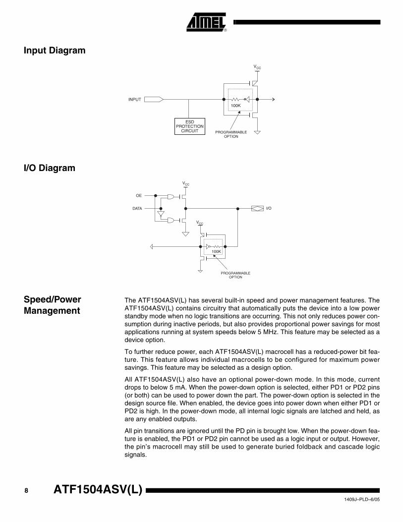
Input Diagram
I/O Diagram
Speed/Power Management
The ATF1504ASV(L) has several built-in speed and power management features. TheATF1504ASV(L) contains circuitry that automatically puts the device into a low powerstandby mode when no logic transitions are occurring. This not only reduces power con-sumption during inactive periods, but also provides proportional power savings for mostapplications running at system speeds below 5 MHz. This feature may be selected as adevice option.
To further reduce power, each ATF1504ASV(L) macrocell has a reduced-power bit fea-ture. This feature allows individual macrocells to be configured for maximum powersavings. This feature may be selected as a design option.
All ATF1504ASV(L) also have an optional power-down mode. In this mode, currentdrops to below 5 mA. When the power-down option is selected, either PD1 or PD2 pins(or both) can be used to power down the part. The power-down option is selected in thedesign source file. When enabled, the device goes into power down when either PD1 orPD2 is high. In the power-down mode, all internal logic signals are latched and held, asare any enabled outputs.
All pin transitions are ignored until the PD pin is brought low. When the power-down fea-ture is enabled, the PD1 or PD2 pin cannot be used as a logic input or output. However,the pin’s macrocell may still be used to generate buried foldback and cascade logicsignals.
8 ATF1504ASV(L)1409J–PLD–6/05

ATF1504ASV(L)
All power-down AC characteristic parameters are computed from external input or I/Opins, with reduced-power bit turned on. For macrocells in reduced-power mode(reduced-power bit turned on), the reduced-power adder, tRPA, must be added to the ACparameters, which include the data paths tLAD, tLAC, tIC, tACL, tACH and tSEXP.
The ATF1504ASV(L) macrocell also has an option whereby the power can be reducedon a per macrocell basis. By enabling this power-down option, macrocells that are notused in an application can be turned down, thereby reducing the overall power con-sumption of the device.
Each output also has individual slew rate control. This may be used to reduce systemnoise by slowing down outputs that do not need to operate at maximum speed. Outputsdefault to slow switching, and may be specified as fast switching in the design file.
Design Software Support
ATF1504ASV(L) designs are supported by several industry standard third party tools.Automated fitters allow logic synthesis using a variety of high-level description lan-guages and formats.
Power-up Reset The ATF1504ASV is designed with a power-up reset, a feature critical for state machineinitialization. At a point delayed slightly from VCC crossing VRST, all registers will be ini-tialized, and the state of each output will depend on the polarity of its buffer. However,due to the asynchronous nature of reset and uncertainty of how VCC actually rises in thesystem, the following conditions are required:
1. The VCC rise must be monotonic,
2. After reset occurs, all input and feedback setup times must be met before driving the clock pin high, and,
3. The clock must remain stable during TD.
The ATF1504ASV has two options for the hysteresis about the reset level, VRST, Smalland Large. To ensure a robust operating environment in applications where the deviceis operated near 3.0V, Atmel recommends that during the fitting process users configurethe device with the Power-up Reset hysteresis set to Large. For conversions, AtmelPOF2JED users should include the flag “-power_reset” on the command line after “file-name.POF”. To allow the registers to be properly reinitialized with the Large hysteresisoption selected, the following condition is added:
4. If VCC falls below 2.0V, it must shut off completely before the device is turned on again.
When the Large hysteresis option is active, ICC is reduced by several hundred micro-amps as well.
Security Fuse Usage A single fuse is provided to prevent unauthorized copying of the ATF1504ASV(L) fusepatterns. Once programmed, fuse verify is inhibited. However, the 16-bit User Signatureremains accessible.
91409J–PLD–6/05

Programming ATF1504ASV(L) devices are in-system programmable (ISP) devices utilizing the 4-pinJTAG protocol. This capability eliminates package handling normally required for pro-gramming and facilitates rapid design iterations and field changes.
Atmel prov ides ISP hardware and sof tware to a l low programming of theATF1504ASV(L) via the PC. ISP is performed by using either a download cable, a com-parable board tester or a simple microprocessor interface.
To facilitate ISP programming by the Automated Test Equipment (ATE) vendors. SerialVector Format (SVF) files can be created by Atmel provided software utilities.
ATF1504ASV(L) devices can also be programmed using standard third-party program-mers. With third-party programmer the JTAG ISP port can be disabled thereby allowingfour additional I/O pins to be used for logic.
Contact your local Atmel representatives or Atmel PLD applications for details.
ISP Programming Protection
The ATF1504ASV(L) has a special feature that locks the device and prevents the inputsand I/O from driving if the programming process is interrupted for any reason. Theinputs and I/O default to high-Z state during such a condition. In addition the pin keeperoption preserves the former state during device programming, if this circuit were previ-ously programmed on the device. This prevents disturbing the operation of other circuitsin the system while the ATF1504ASV(L) is being programmed via ISP.
All ATF1504ASV(L) devices are initially shipped in the erased state thereby makingthem ready to use for ISP.Note: For more information refer to the “Designing for In-System Programmability with Atmel
CPLDs” application note.
10 ATF1504ASV(L)1409J–PLD–6/05
ATF1504ASV(L)
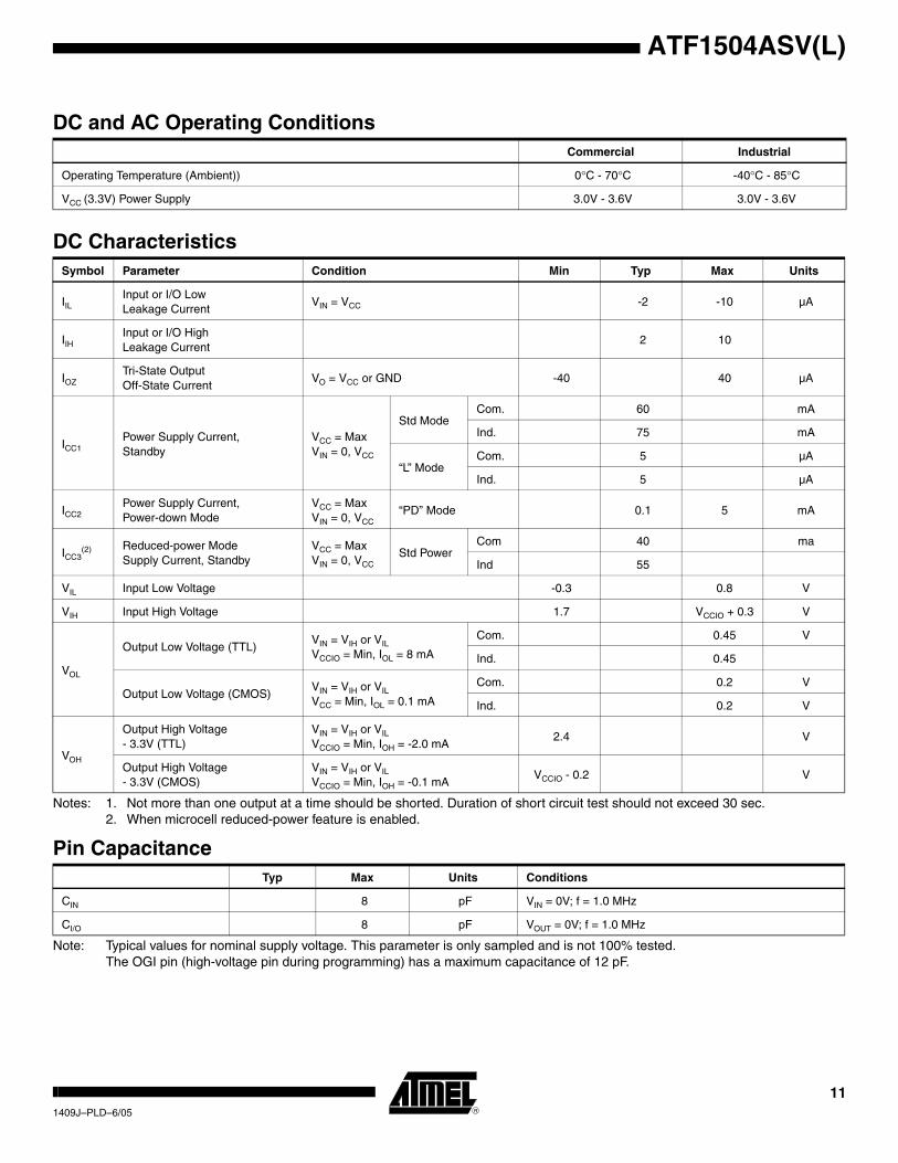
Notes: 1. Not more than one output at a time should be shorted. Duration of short circuit test should not exceed 30 sec.2. When microcell reduced-power feature is enabled.
Note: Typical values for nominal supply voltage. This parameter is only sampled and is not 100% tested.The OGI pin (high-voltage pin during programming) has a maximum capacitance of 12 pF.
DC and AC Operating ConditionsCommercial Industrial
Operating Temperature (Ambient)) 0°C - 70°C -40°C - 85°C
VCC (3.3V) Power Supply 3.0V - 3.6V 3.0V - 3.6V
DC CharacteristicsSymbol Parameter Condition Min Typ Max Units
IILInput or I/O LowLeakage Current
VIN = VCC -2 -10 µA
IIHInput or I/O HighLeakage Current
2 10
IOZTri-State OutputOff-State Current
VO = VCC or GND -40 40 µA
ICC1Power Supply Current,Standby
VCC = MaxVIN = 0, VCC
Std ModeCom. 60 mA
Ind. 75 mA
“L” ModeCom. 5 µA
Ind. 5 µA
ICC2Power Supply Current, Power-down Mode
VCC = MaxVIN = 0, VCC
“PD” Mode 0.1 5 mA
ICC3(2) Reduced-power Mode
Supply Current, StandbyVCC = MaxVIN = 0, VCC
Std PowerCom 40 ma
Ind 55
VIL Input Low Voltage -0.3 0.8 V
VIH Input High Voltage 1.7 VCCIO + 0.3 V
VOL
Output Low Voltage (TTL)VIN = VIH or VILVCCIO = Min, IOL = 8 mA
Com. 0.45 V
Ind. 0.45
Output Low Voltage (CMOS)VIN = VIH or VILVCC = Min, IOL = 0.1 mA
Com. 0.2 V
Ind. 0.2 V
VOH
Output High Voltage- 3.3V (TTL)
VIN = VIH or VILVCCIO = Min, IOH = -2.0 mA
2.4 V
Output High Voltage- 3.3V (CMOS)
VIN = VIH or VILVCCIO = Min, IOH = -0.1 mA
VCCIO - 0.2 V
Pin CapacitanceTyp Max Units Conditions
CIN 8 pF VIN = 0V; f = 1.0 MHz
CI/O 8 pF VOUT = 0V; f = 1.0 MHz
111409J–PLD–6/05
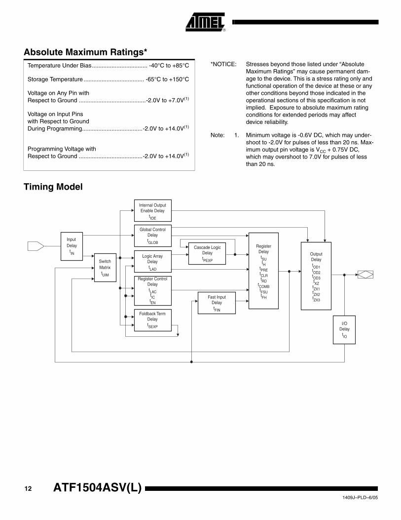
Timing Model
Absolute Maximum Ratings*Temperature Under Bias.................................. -40°C to +85°C *NOTICE: Stresses beyond those listed under “Absolute
Maximum Ratings” may cause permanent dam-age to the device. This is a stress rating only and functional operation of the device at these or any other conditions beyond those indicated in the operational sections of this specification is not implied. Exposure to absolute maximum rating conditions for extended periods may affect device reliability.
Note: 1. Minimum voltage is -0.6V DC, which may under-shoot to -2.0V for pulses of less than 20 ns. Max-imum output pin voltage is VCC + 0.75V DC, which may overshoot to 7.0V for pulses of less than 20 ns.
Storage Temperature ..................................... -65°C to +150°C
Voltage on Any Pin with Respect to Ground .........................................-2.0V to +7.0V(1)
Voltage on Input Pins with Respect to Ground During Programming.....................................-2.0V to +14.0V(1)
Programming Voltage with Respect to Ground .......................................-2.0V to +14.0V(1)
Input Delay
tIN
SwitchMatrixtUIM
Foldback TermDelaytSEXP
Register ControlDelaytLACtICtEN
Logic ArrayDelaytLAD
Global ControlDelaytGLOB
Internal OutputEnable Delay
tIOE
Cascade LogicDelaytPEXP
Fast InputDelaytFIN
RegisterDelaytSUtH
tPREtCLRtRD
tCOMBtFSUtFH
OutputDelaytOD1tOD2tOD3tXZtZX1tZX2tZX3
I/ODelay
tIO
12 ATF1504ASV(L)1409J–PLD–6/05

ATF1504ASV(L)
AC Characteristics
Symbol Parameter
-15 -20
UnitsMin Max Min Max
tPD1 Input or Feedback to Non-Registered Output 3 15 20 ns
tPD2 I/O Input or Feedback to Non-Registered Feedback 3 12 16 ns
tSU Global Clock Setup Time 11 13.5 ns
tH Global Clock Hold Time 0 0 ns
tFSU Global Clock Setup Time of Fast Input 3 3 ns
tFH Global Clock Hold Time of Fast Input 1.0 2 MHz
tCOP Global Clock to Output Delay 9 12 ns
tCH Global Clock High Time 5 6 ns
tCL Global Clock Low Time 5 6 ns
tASU Array Clock Setup Time 5 7 ns
tAH Array Clock Hold Time 4 4 ns
tACOP Array Clock Output Delay 15 18.5 ns
tACH Array Clock High Time 6 8 ns
tACL Array Clock Low Time 6 8 ns
tCNT Minimum Clock Global Period 13 17 ns
fCNT Maximum Internal Global Clock Frequency 76.9 66 MHz
tACNT Minimum Array Clock Period 13 17 ns
fACNT Maximum Internal Array Clock Frequency 76.9 58.8 MHz
fMAX Maximum Clock Frequency 100 83.3 MHz
tIN Input Pad and Buffer Delay 2 2.5 ns
tIO I/O Input Pad and Buffer Delay 2 2.5 ns
tFIN Fast Input Delay 2 2 ns
tSEXP Foldback Term Delay 8 10 ns
tPEXP Cascade Logic Delay 1 1 ns
tLAD Logic Array Delay 6 8 ns
tLAC Logic Control Delay 3.5 4.5 ns
tIOE Internal Output Enable Delay 3 3 ns
tOD1Output Buffer and Pad Delay(Slow slew rate = OFF; VCCIO = 5V; CL = 35 pF)
3 4 ns
tOD2Output Buffer and Pad Delay (Slow slew rate = OFF; VCCIO = 3.3V; CL = 35 pF)
3 4 ns
tOD3Output Buffer and Pad Delay (Slow slew rate = ON; VCCIO = 5V or 3.3V; CL = 35 pF)
5 6 ns
tZX1Output Buffer Enable Delay(Slow slew rate = OFF; VCCIO = 5.0V; CL = 35 pF)
7 9 ns
131409J–PLD–6/05

Notes: 1. See ordering information for valid part numbers.2. The tRPA parameter must be added to the tLAD, tLAC,tTIC, tACL, and tSEXP parameters for macrocells running in the reduced-
power mode.3. See ordering information for valid part numbers.
Input Test Waveforms and Measurement Levels
tR, tF = 1.5 ns typical
Output AC Test Loads
tZX2Output Buffer Enable Delay(Slow slew rate = OFF; VCCIO = 3.3V; CL = 35 pF)
7 9 ns
tZX3Output Buffer Enable Delay(Slow slew rate = ON; VCCIO = 5.0V/3.3V; CL = 35 pF)
10 11 ns
tXZ Output Buffer Disable Delay (CL = 5 pF) 6 7 ns
tSU Register Setup Time 5 6 ns
tH Register Hold Time 4 5 ns
tFSU Register Setup Time of Fast Input 2 2 ns
tFH Register Hold Time of Fast Input 2 2 ns
tRD Register Delay 2 2.5 ns
tCOMB Combinatorial Delay 2 3 ns
tIC Array Clock Delay 6 7 ns
tEN Register Enable Time 6 7 ns
tGLOB Global Control Delay 2 3 ns
tPRE Register Preset Time 4 5 ns
tCLR Register Clear Time 4 5 ns
tUIM Switch Matrix Delay 2 2.5 ns
tRPA Reduced-power Adder(2) 10 13 ns
AC Characteristics (Continued)
Symbol Parameter
-15 -20
UnitsMin Max Min Max
R1 = 703Ω
3.0V
OUTPUT PIN
CL = 35 pFR2 = 8060Ω
14 ATF1504ASV(L)1409J–PLD–6/05

ATF1504ASV(L)
Power-down Mode The ATF1504ASV(L) includes an optional pin-controlled power-down feature. When thismode is enabled, the PD pin acts as the power-down pin. When the PD pin is high, thedevice supply current is reduced to less than 3 mA. During power down, all output dataand internal logic states are latched internally and held. Therefore, all registered andcombinatorial output data remain valid. Any outputs that were in a High-Z state at theonset will remain at High-Z. During power down, all input signals except the power-downpin are blocked. Input and I/O hold latches remain active to ensure that pins do not floatto indeterminate levels, further reducing system power. The power-down mode featureis enabled in the logic design file or as a fitted or translated s/w option. Designs usingthe power-down pin may not use the PD pin as a logic array input. However, all other PDpin macrocell resources may still be used, including the buried feedback and foldbackproduct term array inputs.
Notes: 1. For slow slew outputs, add tSSO.2. Pin or product term.3. Includes tRPA for reduced-power bit enabled.
Power Down AC Characteristics(1)(2)
Symbol Parameter
-15 -20
UnitsMin Max Min Max
tIVDH Valid I, I/O before PD High 15 20 ns
tGVDH Valid OE(2) before PD High 15 20 ns
tCVDH Valid Clock(2) before PD High 15 20 ns
tDHIX I, I/O Don’t Care after PD High 25 30 ns
tDHGX OE(2) Don’t Care after PD High 25 30 ns
tDHCX Clock(2) Don’t Care after PD High 25 30 ns
tDLIV PD Low to Valid I, I/O 1 1 µs
tDLGV PD Low to Valid OE (Pin or Term) 1 1 µs
tDLCV PD Low to Valid Clock (Pin or Term) 1 1 µs
tDLOV PD Low to Valid Output 1 1 µs
151409J–PLD–6/05

JTAG-BST/ISP Overview
The JTAG boundary-scan testing is controlled by the Test Access Port (TAP) controllerin the ATF1504ASV(L). The boundary-scan technique involves the inclusion of a shift-register stage (contained in a boundary-scan cell) adjacent to each component so thatsignals at component boundaries can be controlled and observed using scan testingprinciples. Each input pin and I/O pin has its own boundary-scan cell (BSC) in order tosupport boundary-scan testing. The ATF1504ASV(L) does not currently include a TestReset (TRST) input pin because the TAP controller is automatically reset at power-up.The five JTAG modes supported include: SAMPLE/PRELOAD, EXTEST, BYPASS,IDCODE and HIGHZ. The ATF1504ASV(L)’s ISP can be fully described using JTAG’sBSDL as described in IEEE Standard 1149.1b. This allows ATF1504ASV(L) program-ming to be described and implemented using any one of the third-party developmenttools supporting this standard.
The ATF1504ASV(L) has the option of using four JTAG-standard I/O pins for boundary-scan testing (BST) and in-system programming (ISP) purposes. The ATF1504ASV(L) isprogrammable through the four JTAG pins using the IEEE standard JTAG programmingprotocol established by IEEE Standard 1149.1 using 5V TTL-level programming signalsfrom the ISP interface for in-system programming. The JTAG feature is a programmableoption. If JTAG (BST or ISP) is not needed, then the four JTAG control pins are avail-able as I/O pins.
JTAG Boundary-scan Cell (BSC) Testing
The ATF1504ASV(L) contains up to 68 I/O pins and four input pins, depending on thedevice type and package type selected. Each input pin and I/O pin has its own bound-ary-scan cell (BSC) in order to support boundary-scan testing as described in detail byIEEE Standard 1149.1. A typical BSC consists of three capture registers or scan regis-ters and up to two update registers. There are two types of BSCs, one for input or I/Opin, and one for the macrocells. The BSCs in the device are chained together throughthe capture registers. Input to the capture register chain is fed in from the TDI pin whilethe output is directed to the TDO pin. Capture registers are used to capture activedevice data signals, to shift data in and out of the device and to load data into the updateregisters. Control signals are generated internally by the JTAG TAP controller. The BSCconfiguration for the input and I/O pins and macrocells are shown below.
BSC Configuration for Input and I/O Pins (Except JTAG TAP Pins)
Note: The ATF1504ASV(L) has pull-up option on TMS and TDI pins. This feature is selected asa design option.
16 ATF1504ASV(L)1409J–PLD–6/05

ATF1504ASV(L)
BSC Configuration for Macrocell
01
DQ
0
1
0
1
D Q D Q
CaptureDR
CaptureDR
UpdateDR
0
1
0
1
D Q D Q
TDI
TDI
OUTJ
OEJ
Shift
Shift
Clock
Clock
Mode
TDO
TDO
Pin BSC
Macrocell BSC
Pin
Pin
171409J–PLD–6/05

OE (1, 2) Global OE pins
GCLR Global Clear pin
GCLK (1, 2, 3) Global Clock pins
PD (1, 2) Power-down pins
TDI, TMS, TCK, TDO JTAG pins used for boundary-scan testing or in-system programming
GND Ground pins
VCC VCC pins for the device
ATF1504ASV Dedicated Pinouts
Dedicated Pin44-leadTQFP
44-leadJ-lead
68-leadJ-lead
84-leadJ-lead
100-leadPQFP
100-leadTQFP
INPUT/OE2/GCLK2 40 2 2 2 92 90
INPUT/GCLR 39 1 1 1 91 89
INPUT/OE1 38 44 68 84 90 88
INPUT/GCLK1 37 43 67 83 89 87
I/O /GCLK3 35 41 65 81 87 85
I/O / PD (1,2) 5, 19 11, 25 17, 37 20, 46 14, 44 12, 42
I/O / TDI (JTAG) 1 7 12 14 6 4
I/O / TMS (JTAG) 7 13 19 23 17 15
I/O / TCK (JTAG) 26 32 50 62 64 62
I/O / TDO (JTAG) 32 38 57 71 75 73
GND 4, 16, 24, 36 10, 22, 30, 426, 16, 26, 34,38, 48, 58, 66
7, 19, 32, 42,47, 59, 72, 82
13, 28, 40, 45,61, 76, 88, 97
11, 26, 38, 43,59, 74, 86, 95
VCC 9, 17, 29, 41 3, 15, 23, 353, 11, 21, 31, 35, 43, 53, 63
3,13, 26, 38, 43, 53, 66, 78
5, 20, 36, 41, 53, 68, 84, 93
3, 18, 34, 39, 51, 66, 82, 91
N/C – – – –
1, 2, 7, 9,24, 26, 29, 30,51, 52, 55, 57,72, 74, 79, 80
1, 2, 5, 7, 22,24, 27, 28, 49,50, 53, 55, 70,
72, 77, 78
# of Signal Pins 36 36 52 68 68 68
# User I/O Pins 32 32 48 64 64 64
18 ATF1504ASV(L)1409J–PLD–6/05

ATF1504ASV(L)
ATF1504ASV I/O Pinouts
MC PLC44-leadPLCC
44-leadTQFP
68-leadPLCC
84-leadPLCC
100-lead
PQFP
100-lead
TQFP MC PLC44-leadPLCC
44-leadTQFP
68-leadPLCC
84-leadPLCC
100-lead
PQFP
100-lead
TQFP
1 A 12 6 18 22 16 14 33 C 24 18 36 44 42 40
2 A - - - 21 15 13 34 C - - - 45 43 41
3A/
PD111 5 17 20 14 12 35
C/PD2
25 19 37 46 44 42
4 A 9 3 15 18 12 10 36 C 26 20 39 48 46 44
5 A 8 2 14 17 11 9 37 C 27 21 40 49 47 45
6 A - - 13 16 10 8 38 C - - 41 50 48 46
7 A - - - 15 8 6 39 C - - - 51 49 47
8/TDI
A 7 1 12 14 6 4 40 C 28 22 42 52 50 48
9 A - - 10 12 4 100 41 C 29 23 44 54 54 52
10 A - - - 11 3 99 42 C - - - 55 56 54
11 A 6 44 9 10 100 98 43 C - - 45 56 58 56
12 A - - 8 9 99 97 44 C - - 46 57 59 57
13 A - - 7 8 98 96 45 C - - 47 58 60 58
14 A 5 43 5 6 96 94 46 C 31 25 49 60 62 60
15 A - - - 5 95 93 47 C - - - 61 63 61
16 A 4 42 4 4 94 9248/
TCKC 32 26 50 62 64 62
17 B 21 15 33 41 39 37 49 D 33 27 51 63 65 63
18 B - - - 40 38 36 50 D - - - 64 66 64
19 B 20 14 32 39 37 35 51 D 34 28 52 65 67 65
20 B 19 13 30 37 35 33 52 D 36 30 54 67 69 67
21 B 18 12 29 36 34 32 53 D 37 31 55 68 70 68
22 B - - 28 35 33 31 54 D - - 56 69 71 69
23 B - - - 34 32 30 55 D - - - 70 73 71
24 B 17 11 27 33 31 2956/
TDOD 38 32 57 71 75 73
25 B 16 10 25 31 27 25 57 D 39 33 59 73 77 75
26 B - - - 30 25 23 58 D - - - 74 78 76
27 B - - 24 29 23 21 59 D - - 60 75 81 79
28 B - - 23 28 22 20 60 D - - 61 76 82 80
29 B - - 22 27 21 19 61 D - - 62 77 83 81
30 B 14 8 20 25 19 17 62 D 40 34 64 79 85 83
31 B - - - 24 18 16 63 D - - - 80 86 84
32/TMS
B 13 7 19 23 17 15 64D/
GCLK341 35 65 81 87 85
191409J–PLD–6/05
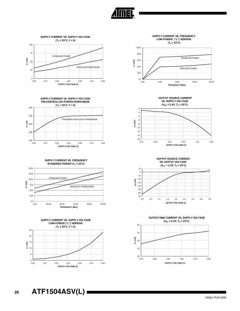
SUPPLY CURRENT VS. SUPPLY VOLTAGE(TA = 25°C, F = 0)
0
25
50
75
100
2.50 2.75 3.00 3.25 3.50 3.75 4.00
SUPPLY VOLTAGE (V)
ICC (m
A)
STANDARD POWER
REDUCED POWER MODE
SUPPLY CURRENT VS. SUPPLY VOLTAGEPIN-CONTROLLED POWER-DOWN MODE
(TA = 25°C, F = 0)
400
500
600
700
800
2.50 2.75 3.00 3.25 3.50 3.75 4.00
SUPPLY VOLTAGE (V)
ICC (u
A) STANDARD & REDUCED POWER MODE
SUPPLY CURRENT VS. FREQUENCY STANDARD POWER (TA = 25°C)
0.0
25.0
50.0
75.0
100.0
125.0
150.0
0.00 20.00 40.00 60.00 80.00 100.00FREQUENCY (MHz)
ICC (m
A)
STANDARD POWER
REDUCED POWER MODE
SUPPLY CURRENT VS. SUPPLY VOLTAGELOW-POWER ("L") VERSION
(TA = 25°C, F = 0)
0
5
10
15
20
25
2.50 2.75 3.00 3.25 3.50 3.75 4.00
SUPPLY VOLTAGE (V)
ICC (u
A)
20 ATF1504ASV(L)
SUPPLY CURRENT VS. FREQUENCY LOW-POWER ("L") VERSION
(TA = 25°C)
0.0
20.0
40.0
60.0
80.0
100.0
0.00 5.00 10.00 15.00 20.00FREQUENCY (MHz)
ICC (m
A)
STANDARD POWER
REDUCED POWER
OUTPUT SOURCE CURRENTVS. SUPPLY VOLTAGE(VOH = 2.4V, TA = 25°C)
-16
-14
-12
-10
-8
-6
-4
-2
0
2.75 3.00 3.25 3.50 3.75 4.00
SUPPLY VOLTAGE (V)
IOH (
mA
)
OUTPUT SOURCE CURRENTVS. OUTPUT VOLTAGE (VCC = 3.3V, TA = 25°C)
-70
-60
-50
-40
-30
-20
-10
0
10
0.0 0.5 1.0 1.5 2.0 2.5 3.0 3.5 4.0
OUTPUT VOLTAGE (V)
IOH (
mA
)
OUTPUT SINK CURRENT VS. SUPPLY VOLTAGE (VOL = 0.5V, TA = 25°C)
20
25
30
35
40
2.75 3.00 3.25 3.50 3.75 4.00
SUPPLY VOLTAGE (V)
IOL (
mA
)
1409J–PLD–6/05

ATF1504ASV(L)
OUTPUT SINK CURRENT VS. OUTPUT VOLTAGE (VCC = 3.3V, TA = 25°C)
0
20
40
60
80
100
0 0.5 1 1.5 2 2.5 3 3.5 4
OUTPUT VOLTAGE (V)
IOL (
mA
)
INPUT CLAMP CURRENT VS. INPUT VOLTAGE (VCC = 3.3V, TA = 25°C)
-100
-80
-60
-40
-20
0
-1 -0.9 -0.8 -0.7 -0.6 -0.5 -0.4 -0.3 -0.2 -0.1 0
INPUT VOLTAGE (V)
INPU
T C
UR
REN
T (m
A)
1409J–PLD–6/05
INPUT CURRENT VS. INPUT VOLTAGE (VCC = 3.3V, TA = 25°C)
-10
-5
0
5
10
15
0 0.5 1 1.5 2 2.5 3 3.5
INPUT VOLTAGE (V)
INPU
T C
UR
REN
T (u
A)
21

Ordering Information
Note: 1. The last time buy is Sept. 30, 2005 for shaded parts.
2. The recommended migration for QC100 or JC68 packages is the AU100 or the smaller JU44 packages. 3. The recommended migration for the JC84 package is the ATF1508ASV-15JU84
Using “C” Product for IndustrialThere is very little risk in using “C” devices for industrial applications because the VCC conditions for 3.3V products are thesame for commercial and industrial (there is only 15°C difference at the high end of the temperature range). To use com-mercial product for industrial temperature ranges, de-rate ICC by 15%.
ATF1504ASV(L) Standard Package OptionstPD
(ns)tCO1
(ns)fMAX
(MHz) Ordering Code Package Operation Range
15 8 100
ATF1504ASV-15 AC44
ATF1504ASV-15 JC44
44A
44J
Commercial(0°C to 70°C)
ATF1504ASV-15 JC68(2)
ATF1504ASV-15 JC84(3)
ATF1504ASV-15 QC100(2)
68J84J
100Q1
ATF1500ASV-15 AC100 100A
15 8 100
ATF1504ASV-15 AI44 44A
Industrial(-40°C to +85°C)
ATF1504ASV-15 JI44 44J
ATF1504ASV-15 JI68
ATF1504ASV-15 JI84ATF1504ASV-15 QI100
ATF1504ASV-15 AI100
68J
84J100Q1
100A
20 12 83.3
ATF1504ASVL-20 AC44
ATF1504ASVL-20 JC44ATF1504ASVL-20 JC68(2)
ATF1504ASVL-20 JC84(3)
ATF1504ASVL-20 QC100(2)
44A
44J68J
84J
100Q1
Commercial
(0°C to 70°C)
ATF1504ASVL-20 AC100 100A
20 12 83.3
ATF1504ASVL-20 AI44ATF1504ASVL-20 JI44
ATF1504ASVL-20 JI68
ATF1504ASVL-20 JI84ATF1504ASVL-20 QI100
ATF1504ASVL-20 AI100
44A44J
68J
84J100Q1
100A
Industrial
(-40°C to +85°C)
22 ATF1504ASV(L)1409J–PLD–6/05

ATF1504ASV(L)
ATF1504ASV(L) Green Package Options (Pb/Halide-free/RoHS Compliant)tPD
(ns)tCO1
(ns)fMAX
(MHz) Ordering Code Package Operation Range
15 8 100
ATF1504ASV-15 AU44 44AIndustrial
(-40°C to +85°C)ATF1504ASV-15 JU44 44J
ATF1504ASV-15 AU100 100A
20 12 83.3ATF1504ASVL-20 AU44ATF1504ASVL-20 JU44
ATF1504ASVL-20 AU100
44A44J
100A
Industrial
(-40°C to +85°C)
Package Type
44A 44-lead, Thin Plastic Gull Wing Quad Flatpack (TQFP)
44J 44-lead, Plastic J-leaded Chip Carrier (PLCC)
68J 68-lead, Plastic J-leaded Chip Carrier (PLCC)
84J 84-lead, Plastic J-leaded Chip Carrier (PLCC)
100Q1 100-lead, 14 x 20 mm Body, Plastic Quad Flat Package (PQFP)
100A 100-lead, 14 x 14 mm Body, Thin Profile Plastic Quad Flat Package (TQFP)
231409J–PLD–6/05

Packaging Information
44A – TQFP
2325 Orchard Parkway San Jose, CA 95131
TITLE DRAWING NO.
R
REV.
44A, 44-lead, 10 x 10 mm Body Size, 1.0 mm Body Thickness,0.8 mm Lead Pitch, Thin Profile Plastic Quad Flat Package (TQFP)
B44A
10/5/2001
PIN 1 IDENTIFIER
0˚~7˚
PIN 1
L
C
A1 A2 A
D1
D
e E1 E
B
COMMON DIMENSIONS(Unit of Measure = mm)
SYMBOL MIN NOM MAX NOTE
Notes: 1. This package conforms to JEDEC reference MS-026, Variation ACB. 2. Dimensions D1 and E1 do not include mold protrusion. Allowable
protrusion is 0.25 mm per side. Dimensions D1 and E1 are maximum plastic body size dimensions including mold mismatch.
3. Lead coplanarity is 0.10 mm maximum.
A – – 1.20
A1 0.05 – 0.15
A2 0.95 1.00 1.05
D 11.75 12.00 12.25
D1 9.90 10.00 10.10 Note 2
E 11.75 12.00 12.25
E1 9.90 10.00 10.10 Note 2
B 0.30 – 0.45
C 0.09 – 0.20
L 0.45 – 0.75
e 0.80 TYP
24 ATF1504ASV(L)1409J–PLD–6/05

ATF1504ASV(L)
44J – PLCC
Notes: 1. This package conforms to JEDEC reference MS-018, Variation AC. 2. Dimensions D1 and E1 do not include mold protrusion.
Allowable protrusion is .010"(0.254 mm) per side. Dimension D1and E1 include mold mismatch and are measured at the extremematerial condition at the upper or lower parting line.
3. Lead coplanarity is 0.004" (0.102 mm) maximum.
A 4.191 – 4.572
A1 2.286 – 3.048
A2 0.508 – –
D 17.399 – 17.653
D1 16.510 – 16.662 Note 2
E 17.399 – 17.653
E1 16.510 – 16.662 Note 2
D2/E2 14.986 – 16.002
B 0.660 – 0.813
B1 0.330 – 0.533
e 1.270 TYP
COMMON DIMENSIONS(Unit of Measure = mm)
SYMBOL MIN NOM MAX NOTE
1.14(0.045) X 45˚ PIN NO. 1
IDENTIFIER
1.14(0.045) X 45˚
0.51(0.020)MAX
0.318(0.0125)0.191(0.0075)
A2
45˚ MAX (3X)
A
A1
B1 D2/E2B
e
E1 E
D1
D
44J, 44-lead, Plastic J-leaded Chip Carrier (PLCC) B44J
10/04/01
2325 Orchard Parkway San Jose, CA 95131
TITLE DRAWING NO.
R
REV.
251409J–PLD–6/05

68J – PLCC
2325 Orchard Parkway San Jose, CA 95131
TITLE DRAWING NO.
R
REV. 68J, 68-lead, Plastic J-leaded Chip Carrier (PLCC) B68J
10/04/01
1.14(0.045) X 45˚ PIN NO. 1
IDENTIFIER
1.14(0.045) X 45˚
0.51(0.020)MAX
0.318(0.0125)0.191(0.0075)
A2
45˚ MAX (3X)
A
A1
B1 D2/E2B
e
E1 E
D1
D
COMMON DIMENSIONS(Unit of Measure = mm)
SYMBOL MIN NOM MAX NOTE
Notes: 1. This package conforms to JEDEC reference MS-018, Variation AE. 2. Dimensions D1 and E1 do not include mold protrusion.
Allowable protrusion is .010"(0.254 mm) per side. Dimension D1and E1 include mold mismatch and are measured at the extremematerial condition at the upper or lower parting line.
3. Lead coplanarity is 0.004" (0.102 mm) maximum.
A 4.191 – 4.572
A1 2.286 – 3.048
A2 0.508 – –
D 25.019 – 25.273
D1 24.130 – 24.333 Note 2
E 25.019 – 25.273
E1 24.130 – 24.333 Note 2
D2/E2 22.606 – 23.622
B 0.660 – 0.813
B1 0.330 – 0.533
e 1.270 TYP
26 ATF1504ASV(L)1409J–PLD–6/05

ATF1504ASV(L)
84J – PLCC
2325 Orchard Parkway San Jose, CA 95131
TITLE DRAWING NO.
R
REV. 84J, 84-lead, Plastic J-leaded Chip Carrier (PLCC) B84J
10/04/01
1.14(0.045) X 45˚ PIN NO. 1
IDENTIFIER
1.14(0.045) X 45˚
0.51(0.020)MAX
0.318(0.0125)0.191(0.0075)
A2
45˚ MAX (3X)
A
A1
B1 D2/E2B
e
E1 E
D1
D
COMMON DIMENSIONS(Unit of Measure = mm)
SYMBOL MIN NOM MAX NOTE
Notes: 1. This package conforms to JEDEC reference MS-018, Variation AF. 2. Dimensions D1 and E1 do not include mold protrusion.
Allowable protrusion is .010"(0.254 mm) per side. Dimension D1and E1 include mold mismatch and are measured at the extremematerial condition at the upper or lower parting line.
3. Lead coplanarity is 0.004" (0.102 mm) maximum.
A 4.191 – 4.572
A1 2.286 – 3.048
A2 0.508 – –
D 30.099 – 30.353
D1 29.210 – 29.413 Note 2
E 30.099 – 30.353
E1 29.210 – 29.413 Note 2
D2/E2 27.686 – 28.702
B 0.660 – 0.813
B1 0.330 – 0.533
e 1.270 TYP
271409J–PLD–6/05

100Q1 – PQFP
PIN 1 ID
A0º~7º
A1
JEDEC STANDARD MS-022, GC-1
PIN 1
09/10/2002
2325 Orchard Parkway San Jose, CA 95131
TITLE DRAWING NO.
R
REV.
100Q1, 100-lead, 14 x 20 mm Body, 3.2 mm Footprint, 0.65 mm Pitch, Plastic Quad Flat Package (PQFP)
B100Q1
COMMON DIMENSIONS(Unit of Measure = mm)
SYMBOL MIN NOM MAX NOTE
A – 3.04 3.4
A1 0.25 0.33 0.5
D 23.20 BSC
E 17.20 BSC
E1 14.00 BSC
B 0.22 – 0.40
D1 20 BSC
L 0.73 – 1.03
e 0.65 BSC
L
E1
C
D
D1
B
e
E
28 ATF1504ASV(L)1409J–PLD–6/05

ATF1504ASV(L)
100A – TQFP
2325 Orchard Parkway San Jose, CA 95131
TITLE DRAWING NO.
R
REV.
100A, 100-lead, 14 x 14 mm Body Size, 1.0 mm Body Thickness,0.5 mm Lead Pitch, Thin Profile Plastic Quad Flat Package (TQFP)
C100A
10/5/2001
PIN 1 IDENTIFIER
0˚~7˚
PIN 1
L
C
A1 A2 A
D1
D
e E1 E
B
A – – 1.20
A1 0.05 – 0.15
A2 0.95 1.00 1.05
D 15.75 16.00 16.25
D1 13.90 14.00 14.10 Note 2
E 15.75 16.00 16.25
E1 13.90 14.00 14.10 Note 2
B 0.17 – 0.27
C 0.09 – 0.20
L 0.45 – 0.75
e 0.50 TYP
Notes: 1. This package conforms to JEDEC reference MS-026, Variation AED. 2. Dimensions D1 and E1 do not include mold protrusion. Allowable
protrusion is 0.25 mm per side. Dimensions D1 and E1 are maximum plastic body size dimensions including mold mismatch.
3. Lead coplanarity is 0.08 mm maximum.
COMMON DIMENSIONS(Unit of Measure = mm)
SYMBOL MIN NOM MAX NOTE
291409J–PLD–6/05

Revision History
Revision Comments
1409J Green package options added.
30 ATF1504ASV(L)1409J–PLD–6/05
Printed on recycled paper.
1409J–PLD–6/05 xM
Disclaimer: The information in this document is provided in connection with Atmel products. No license, express or implied, by estoppel or otherwise, to anyintellectual property right is granted by this document or in connection with the sale of Atmel products. EXCEPT AS SET FORTH IN ATMEL’S TERMS AND CONDI-TIONS OF SALE LOCATED ON ATMEL’S WEB SITE, ATMEL ASSUMES NO LIABILITY WHATSOEVER AND DISCLAIMS ANY EXPRESS, IMPLIED OR STATUTORYWARRANTY RELATING TO ITS PRODUCTS INCLUDING, BUT NOT LIMITED TO, THE IMPLIED WARRANTY OF MERCHANTABILITY, FITNESS FOR A PARTICULARPURPOSE, OR NON-INFRINGEMENT. IN NO EVENT SHALL ATMEL BE LIABLE FOR ANY DIRECT, INDIRECT, CONSEQUENTIAL, PUNITIVE, SPECIAL OR INCIDEN-TAL DAMAGES (INCLUDING, WITHOUT LIMITATION, DAMAGES FOR LOSS OF PROFITS, BUSINESS INTERRUPTION, OR LOSS OF INFORMATION) ARISING OUTOF THE USE OR INABILITY TO USE THIS DOCUMENT, EVEN IF ATMEL HAS BEEN ADVISED OF THE POSSIBILITY OF SUCH DAMAGES. Atmel makes norepresentations or warranties with respect to the accuracy or completeness of the contents of this document and reserves the right to make changes to specificationsand product descriptions at any time without notice. Atmel does not make any commitment to update the information contained herein. Unless specifically providedotherwise, Atmel products are not suitable for, and shall not be used in, automotive applications. Atmel’s products are not intended, authorized, or warranted for useas components in applications intended to support or sustain life.
Atmel Corporation Atmel Operations
2325 Orchard ParkwaySan Jose, CA 95131, USATel: 1(408) 441-0311Fax: 1(408) 487-2600
Regional Headquarters
EuropeAtmel SarlRoute des Arsenaux 41Case Postale 80CH-1705 FribourgSwitzerlandTel: (41) 26-426-5555Fax: (41) 26-426-5500
AsiaRoom 1219Chinachem Golden Plaza77 Mody Road TsimshatsuiEast KowloonHong KongTel: (852) 2721-9778Fax: (852) 2722-1369
Japan9F, Tonetsu Shinkawa Bldg.1-24-8 ShinkawaChuo-ku, Tokyo 104-0033JapanTel: (81) 3-3523-3551Fax: (81) 3-3523-7581
Memory2325 Orchard ParkwaySan Jose, CA 95131, USATel: 1(408) 441-0311Fax: 1(408) 436-4314
Microcontrollers2325 Orchard ParkwaySan Jose, CA 95131, USATel: 1(408) 441-0311Fax: 1(408) 436-4314
La ChantrerieBP 7060244306 Nantes Cedex 3, FranceTel: (33) 2-40-18-18-18Fax: (33) 2-40-18-19-60
ASIC/ASSP/Smart CardsZone Industrielle13106 Rousset Cedex, FranceTel: (33) 4-42-53-60-00Fax: (33) 4-42-53-60-01
1150 East Cheyenne Mtn. Blvd.Colorado Springs, CO 80906, USATel: 1(719) 576-3300Fax: 1(719) 540-1759
Scottish Enterprise Technology ParkMaxwell BuildingEast Kilbride G75 0QR, Scotland Tel: (44) 1355-803-000Fax: (44) 1355-242-743
RF/AutomotiveTheresienstrasse 2Postfach 353574025 Heilbronn, GermanyTel: (49) 71-31-67-0Fax: (49) 71-31-67-2340
1150 East Cheyenne Mtn. Blvd.Colorado Springs, CO 80906, USATel: 1(719) 576-3300Fax: 1(719) 540-1759
Biometrics/Imaging/Hi-Rel MPU/High Speed Converters/RF Datacom
Avenue de RochepleineBP 12338521 Saint-Egreve Cedex, FranceTel: (33) 4-76-58-30-00Fax: (33) 4-76-58-34-80
Literature Requestswww.atmel.com/literature
© Atmel Corporation 2005. All rights reserved. Atmel®, logo and combinations thereof, Everywhere You Are® and others, are registered trade-marks or trademarks of Atmel Corporation or its subsidiaries. Other terms and product names may be trademarks of others.