Embed Size (px)
Citation preview
The magazine for people who build electronic projects
AVER L ACTION PROJECTS LET YOU..
Spot your car's RPM indication on an LED Analog Disply
Convert your TV receiver to a Video Terminal
Assemble new projects on our
Universal Designer Discover backyard Buried Treasure
Pull in SSB signals on your CB AM Rig
Design cheapie binary -to -hex LED Displays
PLUS Power Supply Projects for
every Workbench Timer Circuits for
Darkroom and Alarm Automatic Game Gadget tells
who was first
o
71896 4878 i
Tracer To
for cab track'
See p
1
#5 $2.25
WINTER 1983
Build Projects from Parts you can buy today!
CompuSound brings e to computer games
See page 22
shmeter es direct
robe/lens readouts
See page 47
Cw Monitor
pulls in your dits and dots See page 81
Xtal Spotter pinpoints shortwave frequencies
See page 44
-k Ic * * * * -k * * -0( * -er
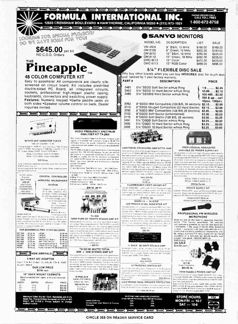
FORMULA INTERNATIONAL INC. 12603 CRENSHAW BOULEVARD HAWTHORNE, CALIFORNIA 90250 (213) 973-1921
PHONE ORDERS ONLY CALL TOLL FREE
1.800-672.8758
e ° ° Pfd OJLQ4gV LOOC3 e COQ SPINUAL
O SIC, NAVE SOME [BOOR YOM
$645.00 per kit NO C.O.D. Orders
TH E
Pineapple
CRYSTAL CONTROLLED
WIRELESS MICROPHONE
SYSTEM
Transmdter FET rmc for Ile, 30-18 KHz response Orai conrrolled 49 MHz AM Band for dish -free performance 100
MW output (range apps.. '/. mdel f or reliable long
range trensmrs sron Powered byn 9V rades battery r in
eluded) Receever_Xtal con
MURA WMS-49 'rolled locks on 49 MHz transmItter signal On panel VU meter. moaitors the signal strength from the mecrophone Standard phone l,. outlet connection to a PA. or other phone snout 9V battery ncluded Thss prolessronal set Is Ideal for on stage, le field church, In house or outdoor use
48 COLOR COMPUTER KIT TM
Easy to assemble! All components are clearly silk- screened on circuit board. Kit includes predrilled double -sided PC Board, all integrated circuits, sockets, professional high -impact plastic casing, keyboards, connectors and switching power supply. Features: Numeric keypad Game paddle jacks on both sides Speaker volume control on back. Dealer inquiries invited.
SANYO MONITORS MODEL NO.
VM 4509 DM 5109 DM 8012 DM 8112 DMC 6013 DMC 6113
DESCRIPTION
9"B&W,10MHz 9" Green, 10 MHz 12" B&W, 18 MHz 12" Green, 18 MHz 13" Color 13" RGB Color
LIST SALE
$190.00 $169.00 $200.00 $180.00 $250.00 $225.00 $260.00 $235.00 $470.00 $425.00 $995.00 $895.00
51/4" FLEXIBLE DISC SALE by buy other brands when you can buy MEMOREX disc for much
and backed by 1 year factory warranty. PART #
`T 3481 3483 3485
3062 "T 3015
3090
'"º'" SC { +-'A s- t
SANYO UHF VARACTOR TUNER FOR UHF CHANNEL 1483
Tuning voltage +1-+28VDC Input impedance 75.0 IF band width 7.16MHz Noise figure 115áB Max Srze 2%" .1Y. x
V Supply voltage 15VDC Sound IF=58.0MHz.
Model 115.8.403A, Video IF 45.OMHz Model 115 -B -405A, Video IF 62.5MHz
$35.00 ea.
Tuner ,s the most Important pan of the cocue. Dont let those 519.00 tuners fool you. All unets are brand new from Sanyo When ordering please %peels model number
No FCC Lleense Requ Bred
OUR PRICE
$49.50 ADDITIONAL
MICROPHONE IT RANSM ITTE RI
AVAILABLE AT $28.00 EACH
(
AUDIO FREQUENCY SPECTRUM ANALYSER KIT TA -2900
The Audso Frequency Spectrum Analyser analyses audio signals Tn 10 octaves over a dynamic range of 30 dB The technique allows the sound "coloration introduced by unwanted room and speaker resonances to be substantially eliminated The TA -29W provides a visual presenlatson of the changing spectrum tnru 100 red LED dIsplays So you can actually see pr0o1 of the equals zed sound you ve achieved The TA -2900 kr Comes with all the eleclronsc components. I C prednlled PC board the Instructsons and a 19" Rack Mount type metal cabinet troth professional selkscreen printed Iront panel SpcdsCahons
Input Sensetvdy Tape Mondor 10mV - 1 BmV 50K Ohms Speaker TerminairO 2W - 100W 8 Ohms
Deplay Level Range lall octaves) 2de per steps -14áB toads Delay Time 11 Kh11 Fast.tBdBis Slow1Rders Power Input 117V or 220V AC 50160 Hz Power Consumption 36W Dimenssons a821W1 102IH1' 2501131 rem
$99.50 per kit
3102 3115 3491 3493 3495
DESCRIPTION PRICE
less
51/4"SSDD Soft Sector w/Hub Ring 1.9 $2.45 51/4"SSDD 10 Hard Sector w/Hub Ring 10.99 $2.15 51/4"SSDD16 Hard Sector w/Hub Ring 100.499 $2.00
500 & up .. call 10psc. 100pcs.
8"SSSD IBM Compatible (128 BIS, 26 sectors) $2.15 $2.00 8"SSSD Shugart Compatible (32 Hard Sector) $2.15 $2.00 8"SSDD IBM Compatible (128 B/S 26 Sectors) $2.85 $2.65 8"DSDD Soft Sector (Unformatted) $3.30 $3.05 8"DSDD Soft Sector (128 B/S, 26 sectors) $3.50 $3.25 51/4 "DSDD Soft Sector wlHub Ring 51/4"DSDD 10 Hard Sector w/Hub Ring 51/4"DSDD 16 Hard Sector wlHub Ring
LOW TIM DC STEREO PRE -AMP KIT TA -1020 Incorporates brand.new DC design that glues a frequency tes' ponse from 0-100Khz ±0.5dB. Added features hke tone de. feat and loudness control let you taslor your own frequency supplies to etimenale power lluctuatronl Specshcations THO/TIM less than .005'X. Frequency response b esponse DC to 10OKHz ±O SdB RIAA devsaon 30 2dB
S/N ralla better than 70dß Sensetluny Phono 2mV 47K/ Au. 100mV 100K Output level 1 3V Max output I5V
Tone controls Bass±10dBOa SOHz/Trehle±1OdBf 15Hz Power supply ±24VDC ua 0.5A. KIt rornes wrth regulated
power supply. all you need Is a 48VCT transformer ea 0 5A
Only S44.50 Xd slues
54.50 ea
FOR COMMERCIAL FREE TV BOX BUILDERS
MC1358....53.00 ea. MC1350.... $2.25 ea. MC1330.. $3.00 ea. MC1496 .... 52.50 ea. MC1458.... 51.00 ea. LM1889 5175 ea. NE565 52.19 ea. N E564. $3.45 ea.
LM380 $200 ea. LM7815 $1,20 ea. LM7818 $1.20 ea. 101(107 P.C. Mount $3.00 ea. 10K1T P.C. Mount $1.75 ea. Torpid Coils (set of 4) $3.00 ea. 5-35pF (Trimmer Cap) 85 ea. Power Transformer 180.8A53 50 ea
TA -800 120W PURE DC POWER STEREO AMP KIT
Getting power hungry from your small amp> Have to watch your budget, Here's a good solution' The TA -800 es a pure DC aroplIfer wen a butt Ie pre -amp. All coupleng capacemrs are elem mated to glue you a true reproduction of the muses. On board tone and volume controls combsned with burn In power supply make the TA -800 the most compact stereo amp evad- able Specshcatmns: 60W a 2 into 80 Freq. range 0-100KHz ±308 THD 01%or better S/N retto, 80dB. Sens,hwty 3mV Imo 47K Power Requirement 324.40 Vohs
A GOOD BUY
at 565.00
FLUORESCENT LIGHT DRIVER KIT 12V DC POWERED 'Ants up 8.15 Watt Fluorescent Light Tubes. Ideal for camper. outdoor. auto or boat Kst Includes he voltage coil power transistor heat sink. all other else home pans and PC Board Light tube not Included.
SS. 50 Per Kit
$3.25.... $3.00 $3.25.... $3.00 $3.25.... $3.00
PROFESSIONAL REGULATED VARIABLE DC POWER SUPPLY KIT
All soled state cucmiry with hegh ensceency power transistor 250388 and IC voltage regulator MC1733 Output voltage an be adjusted from 0-30V at IA current limned or 0.150 e,
2A cu nt horned. Internal re s less than 0.00511. apple rand noise less than lmV, dual on panel meters for voltage and amp reading. also with on board LED and audeble over load Indicator. KIt comes with pre -dulled PC Board. nstructlons. all necessary electronic components. transfor-
mer a prolessronal looking metal cabinet The best pro, lest for school and the most useful Instrument for repairmen Budd one today
MODEL TR88A 0-15VDC @ 2A MODEL TR88B 0-30VDC @ 18
$59.50 Per Kit
CFNEW ARRtVALS VVV
6 -WAY A/C ADAPTOR Input: 110v A/C Output. 3v, 4.5v. 6v, 7.5v 8 12vDC Current: 300mA
OUR LOW PRICE $5.50 each
19" RACK MOUNT CABINETS Black anodized front panel with black leztured case.
WIDTH DEPTH HEIGHT 17"
17" 17"
111/2" 111/2" 111/2"
PRICE
$25.50 $31.50 $39.50
TA -323 60 WATTS TOTAL 30W + 30W STEREO AMP KIT
TMs es a soled state all transestor csrcuitry wsth on board stereo pre -amp for most mscrophone or phone Input. Power output employs 2 parrs matcheng Darlington Transistors driven by the popular 2N3053 Dreyer Transistors. Four burr on board controls for. volume, balance, treble and bass. Power supply requites 48VCT 2.5A transformer. THD of less than 0.1% bet- ween 100Hz-tOKhz at lull power (30 Watts + 30 Watts loaded Into 80)
Minimum Order $10.00 1 Celli. Residents add 6.5 Sales Tas. Phone Orden Accepted on VISA or MC ONLY, NO C-O.D.'s. Prices subject to change without notice.
-1r -X -fr * * *
*SPECIAL* EXCELLENT PRICE.
MODEL 001-0034 $29.50 Per Kit
Transformer 510.50 ea. S
I P`c
MARK IV - 15 STEP LED POWER LEVEL INDICATOR KIT
The new stereo level sndscatur kit <onsests o136 4 -color LED s
(15 per channel) to mdse ate one sound level output of your amplifier from -36dß 10 +3dB Comes wslh a well desegned silk screen panted plastic panel and has a selector switch In allowlloalsng or gradual output Indscating Power supplyes6- 12VDC with THG on board maul sensmwly controls This unit can work with any ampldser from 1 W to 200WI KIl Includes 70 pcs drover transistors. 38 pcs matched 4.color LED s, all other electronic <, mponents, PC Board and front panel
MARK IV KIT
$31.50
"FISHER" 30 WATT STEREO AMP MAIN AMP I I 5 x 21 Ksl includes 2 pcs. Fssher PA 301 Hybrid IC, all electronec pans with PC Board. Power supply ±16VDC (not Included) Power band wsth (KF I%*3dB) Voltage gam 3346 20Hz-20K Hz
Super Buy Only $18.50
POWER SUPPLY KIT 0.30VDC REGULATED. Uses UA723 and 2N3055 power
sestor. Output can be adlusted from 0-30V @ 2A. Com- plete weih PC Board and all elecironsc pans
TRANSFORMER $9.50 ee
POWER SUPPLY KIT $10.50 ea.
01111111 PROFESSIONAL FM WIRELESS
MICROPHONE Made by one of the leading Japanese manufac Curers. This factory assembled FM wireless microphone is powered by two AA size batteries. It transmits In the range of 86-108 MHz. Element is built in a plastic tube type case with an omni- directional electronic condensor microphone unit. By using a standard FM radio, signal can be heard anywhere on a one -acre lot. Sound quality was judged "very good." MODEL WEM -36. WAS $16.50 ON SALE 512.50 each
ULTRASONIC SWITCH KIT Kit Includes the Ultra Sonic Transducers. 2 PC Boards for transmdter and recescer. all electronic pans and Inshucuons Easy to build and a lot of uses such as remote control for TV. garage door alarm system or counter Umt operates by 9.12VDC 515.50 ea.
ELECTRONIC DUAL SPEAKER PROTECTOR Cuts o9 when cncun Is shoved or over loaded to protect your ampiIlse, as well as your speakers A must for OCL urcusts
KIT FORM $8.75 ea.
SHIPPING AND HANDLING CHARGES Under 550.00 Purchase Over 050.00 Purchase
Inside Callforn,e 10% 5% Outside Celif. (Inc'. Mexico Et Commie) 15% 10% Overseas 25% 20%
TA1000 KIT
S51.95 Power Transformer
$24.00 a. 100W CLASS A POWER AMP KIT
Dyne ,c Bees Class "A" c un design makes this unit uneque n its class. Crystal clear. 100' wens power output will satisfy
the most picky fans. A perfect combination with the TA -1020 low TIM stereo pre -amp. Speuhcabons: Output power 100W RMS telo en. 125W RMS into 40 Frequency response 109e -10064e THD less than 0.008% 5/N rare better than Bode Input sen- sitlurty 1V max. Power supply ±400 @ 5A.
STORE HOURS MON-FRI - 10.7 ri h _ SAT - 10.6 II,1
CIRCLE 203 ON READER SERVICE CARD
Radio - Electronics `
o
#5 WINTER
Input is needed for Output You now have our fifth issue of Special Projects in your hands and you may be thinking that "the
Publisher at Radio Electronics is seriously planning to produce this unique magazine on a regular basis." The words between the quotes are actually from a reader's letter and he is absolutely correct!
Yes, you can fully expect to see Special Projects on the newsstand regularly during the year 1983. What we would like to know is: How many issues a year would you be likely to purchase? And, would you be willing to pay for a full -price subscription to insure your receiving every issue published in 1983?
These are important questions for you to answer. With your input data we can make very fruitful decisions in 1983 that will bring to many of you scores upon scores of exciting, useful, pleasurable, and educational hours building electronic projects, and from a deca-to a kilo -times that of reliable and entertaining hours of project application
So, please, write to me at the address given below stating how many issues of Special Projects you would like to purchase in 1983, and your preference to a full -price (sure -to -get) subscription or taking the chance on finding the magazine on your local newsstand before it is sold out.
But, before you write, thumb through the pages of this issue of Special Projects. Take a look at Glitch Stretcher on page 90. This is one of my testbench favorites that adds new life to low-cost or older oscilloscopes. Lock -Out on page 63 is a novel circuit with countless parlor -game and shop applications, when you must know who or what was first! And, if you constantly use a strobe for studio -like photography at home, check our Flashmeter on page 47. If you miss a snap with this gadget, it's only because you left the lens cover on. And, the pieée de résistance is Light Sequencer on page 71. That project is a must for me this Christmas to effect a very unusual holiday window lighting effect. I have plans of making Santa's sleigh appear to be moving!
OK-now you get moving, find your favorites in this issue, and see if we think alike. Let me know your views when you write to me about Special Projects!
Radio -Electronics Special Projects, (ISSN 0033-7862) published quarterly by Gernsback Publications, Inc., 200 Park Avenue South, New York, NY 10003. Phone 212-777-6400. No subscriptions. Single -copy price $2.25. © 1982 by Gernsback Publications Inc. All rights reserved. Printed in U.S.A.
Julian S. Martin, KA2GUN Managing Editor
Gernsback Publications, Inc. Special Projects, Suite 1101 200 Park Avenue South New York, New York 10003
A stamped self-addressed envelope must accompany all submitted manuscripts and/or artwork or photographs if their return is desired should they be rejected. We disclaim any responsibility for the loss or damage of manuscripts and/or artwork or photographs while in our possession or otherwise.
As a service to readers, Radio -Electronics Special Projects publishes available plans or information relating to newsworthy products, techniques and scientific and technological developments. Because of possible variances in the quality and cordition of materials and workmanship used by readers, Radio -Electronics Special Projects disclaims any responsibility for the safe and proper functioning of reader -built projects based upon or from plans or information published in this magazine.
Radio- Eleot n. awl
25 TV TO VIDEO
MONITOR Here are the tips and techniques to convert a television receiver to a video monitor for your compu ter. But, before you pull off the back cover, read this article to discover that the conversion is not that easy!
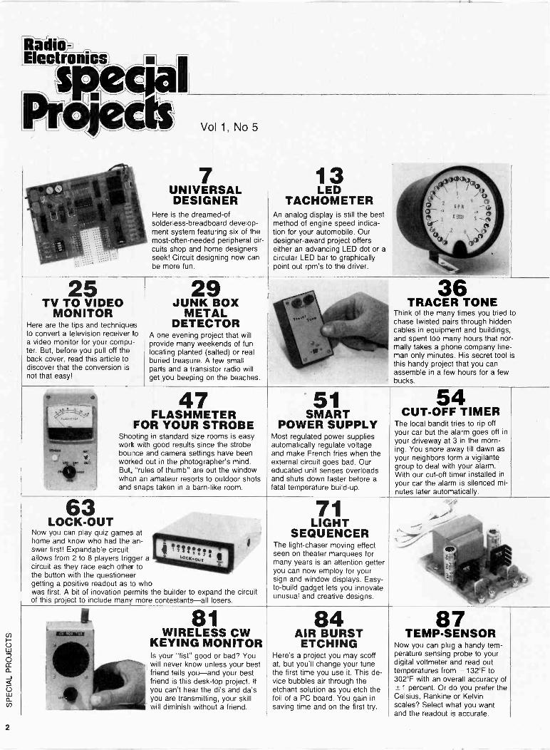
Vol 1, No 5
7 UNIVERSAL DESIGNER
Here is the dreamed -of solderless-breadboard develop- ment system featuring six of the most -often -needed peripheral cir- cuits shop and home designers seek! Circuit designing now can be more fun.
29 JUNK BOX
METAL DETECTOR
A one evening project that will provide many weekends of fun locating planted (salted) or real buried treasure. A few small parts and a transistor radio will get you beeping on the beaches.
13 LED
TACHOMETER An analog display is still the best method of engine speed indica- tion for your automobile. Our designer -award project offers either an advancing LED dot or a circular LED bar to graphically point out rpm's to the driver.
36 TRACER TONE
Think of the many times you tried to chase twisted pairs through hidden cables in equipment and buildings, and spent too many hours that nor- mally takes a phone company line- man only minutes. His secret tool is this handy project that you can assemble in a few hours for a few bucks.
47 FLASHMETER
FOR YOUR STROBE Shooting in standard size rooms is easy work with good results since the strobe bounce and camera settings have been worked out in the photographer's mind. But, "rules of thumb" are out the window when an amateur resorts to outdoor shots and snaps taken in a barn -like room.
51 SMART
POWER SUPPLY Most regulated power supplies automatically regulate voltage and make French fries when the external circuit goes bad. Our educated unit senses overloads and shuts down faster before a fatal temperature build-up.
54 CUT-OFF TIMER
The local bandit tries to rip off your car but the alarm goes off in
your driveway at 3 in the morn- ing. You snore away till dawn as your neighbors form a vigilante group to deal with your alarm. With our cut-off timer installed in your car the alarm is silenced mi- nutes later automatically.
63 LOCK-OUT
Now you can play quiz games at home and know who had the an- swer first! Expandable circuit allows from 2 to 8 players trigger a circuit as they race each other to the button with the questioneer getting a positive readout as to who was first. A bit of inovation permits the builder to expand the circuit of this project to include many more contestants-all losers.
81 WIRELESS CW
KEYING MONITOR Is your "fist" good or bad? You will never know unless your best friend tells you-and your best friend is this desk -top project. If
you can't hear the di's and da's you are transmitting, your skill will diminish without a friend.
71 LIGHT
SEQUENCER The light -chaser moving effect seen on theater marquees for many years is an attention getter you can now employ for your sign and window displays. Easy - to -build gadget lets you innovate unusual and creative designs.
84 AIR BURST ETCHING
Here's a project you may scoff at, but you'll change your tune the first time you use it. This de- vice bubbles air through the etchant solution as you etch the foil of a PC board. You gain in saving time and on the first try.
87 TEMP -SENSOR
Now you can plug a handy tem- perature sensing probe to your digital voltmeter and read out temperatures from -132°F to 302°F with an overall accuracy of ± 1 percent. Or do you prefer the Celsius, Rankine or Kelvin scales? Select what you want and the readout is accurate.
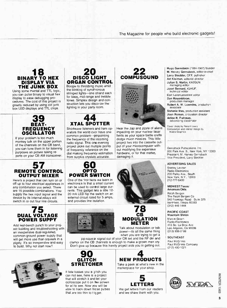
18 BINARY TO HEX
DISPLAY VIA THE JUNK BOX
Using some mental and TTL logic, you can pulse binary to visual hex display to ease debugging pro- cedures. The cost of this project is greatly reduced by using old junk box LED displays and TTL chips.
20 DISCO LIGHT
ORGAN CONTROL Boogie to throbbing music amid the blinking of synchronous stringed lights -one strand each for bass, mid -range and trebble tones. Simplex design and con- struction lets you disco-ize the lighting in your party room.
39 BEAT-
FREQUENCY OSCILLATOR
If your problem is too much monkey talk on the upper portion of the channels on the CB band, you can tune them in for listening purposes as picture taking re- ports on your CB AM transceiver.
44 XTAL SPOTTER
Shortwave listeners and ham op- erators the world over have one common problem-pinpointing the frequency of the incoming radio signal. This ore -evening project picks out multiple points of frequency reference on the dial making frequency estimation from surplus crystals accurate.
The Magazine for people who build electronic gadgets!
22 COMPUSOUND
Hear the zap and zizzle of aliens impacting on your nuclear laser fields as your space battle crafts dodge muon missiles. This little project ties into the cassette out- put of your microcomputer with- out modifying the expensive hardware, or for that matter, damaging it.
57 REMOTE CONTROL
OUTPUT MIXER Here's a project that can turn on or off up to four electrical appliances in any combination you select. There are 16 possible combinations. You supply the hex input signal and the device by its internal relays will switch in or out four line circuits.
60 OPTO
POWER SWITCH One of the first facts we learn in
electronics is that a small current can be used to control large cur- rents. This gadget lets a little 12- 20 mA LED flip the switch on an external circuit rated for 5 amps, and provides line isolation.
75 DUAL VOLTAGE POWER SUPPY
Add test -bench punch to your proj- ect building and troubleshooting with an inexpensive dual -regulated, common -ground power supply that wilt get more use than squeals in a pigsty. It's so inexpensive and easy to build. Why not start now?
78 CB
MODULATION METER
Talk about modulation or talk power-its all the same thing when you are trying to get a
pip-squeak signal out of your CB set and the RF din and clamor on the CB 2hannels is enough to make a grown man cry. Don't give up because this handy project aids you in getting out.
90 GLITCH
STRETCHER If fate tosses you a gl tch you can not see, here is a project that will stretch it and let your ocilloscope put it on the screen for all to see. Now you will be able to track down these pulses that are too thin to t-içger.
4 NEW PRODUCTS
Take a peek at what's new in the marketplace for your shop.
5 LETTERS
We get letters from our readers and we share them with you.
Hugo Gernsback (1884-1967) founder M. Harvey Gernsback, editor -in -chief Larry Steckler, CET, publisher Art Kleiman, editorial director Julian S. Martin, KA2GUN
managing editor Josef Bernard, K2HUF,
technical editor Carl Laron,assistant editor Dan Rosenbloom,
production manager Robert A. W. Lowndes, production
associate Stefanie Mas, production assistant Joan Roman, circulation director Arline R. Fishman,
advertising coodinator
Cover photo by Robert Lewis Composition and interior design by
Mates Graphics
Gernsback Publications, Inc. 200 Park Ave. S., New York, NY 10003 President: M. Harvey Gernsback Vice President; Larry Steckler
ADVERTISING SALES
Stanley Levitan Radio -Electronics 200 Parks Ave., South New York, N.Y., 10003 212-777-6400
MIDWEST/Texas/ Arkansas/Okla. Ralph Bergen The Ralph Bergen Co. 540 Frontage Road-Suite 325 Northfield, Illinois 60093 (312) 446-1444
PACIFIC COAST Mountain States Marvin Green Radio -Electronics 413 So. La Brea Ave. Los Angeles, Ca 90036 (213) 938-0166
SOUTHEAST Paul McGinnis Paul McGinnis Company (212) 490-1021
3
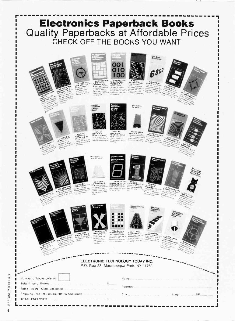
r Electronics Paperback Books
Quality Paperbacks at Affordable Prices CHECK OFF THE BOOKS YOU WANT
eke ose
.
NO IS
ooi 010 IOo
p,lECTS FOR ANINTROL, I,t,r. to 'Mt. l.,.,lTDE AMICROP-
TO BASIC PRO- TO DIGITAL 1ECN- ROCESSOR PRIMER PAID BDATS Sra NG 'TECH-
Pear C$pacq Po I
NIQUES 55.'1. Based a
We sloe o5 ces, pur ng ne
n Tire authors own e. 0Onnng to all Me gl a
áB09 m,c
pe PCe nnn Teaming s cad, C composer aro e.pta,mry ºuc Ar
BASIC and m helPnnng aas You need b know .n I,on ana prpgrlrorl
la09rslo uMerslaM !tonics world
e,gnaT elec- slrucb e and operabah s'
me laryuage rd
BlootraNc Circuits Book 1
POPULAR POPULAR
ELECTRONIC ELECTRONIC PROJECTS-Book PROJECTS Book I
thatS5.0 circuits More es SS15Da_voum Latest
e eel urld on me P eced,ne vosvme More protects lar the
nohd'rsI
Board aolPcts
MINI-MATRIA BOARD PROJECTS 5500. 20 circuits Yoe
dead on a Vo yo Cole can tonna exam L áD
te ̂e magnetic belt ands.
1] hers
MPLELEO I, 3
RADIOCIRCUI USINGtICsa_ S15.
PSIT UMo qaM Io
.ecnne er. tor AM
"^ ar FM s,onats
a p t a da°.,der: dr,pnom< n<Inded
Now to Uaº Op 4mpg
NOW TO USE OP AMPS 55.15. A Ues,gm !s guide Inas comemes
keel e book
beak i Ca0lle br pectOrkular,ons
COUNTER DRIVER SINGLE IC
PROJECTS 54. PROJECTS Sa. very
TRANSIS, k, ds pi a sole's are l
e rC mPNDUEC
described and circuits Eue' rto Id I Fun r °doleº for usnnng them use nowroe
Moot
PROJECTS FOR ELECTRONIC BEGINNERS 53.15. TIMER PROJECTS
PRwill55. JEC Newcomers w, tine 0e. Man' POes,nnne
s book a great way lo aopheations
gel d There are rep Sim
without soldern cludeo utl oquds are ' to
Number of books ordered
Total Price of Books
Sales Tax (NY State Residents)
ELECTRONIC TECHNOLOGY TODAY INC. P.O. Box 83, Massapequa Park. NY 11762
Shipping (75c 1st 2 books, 300 ea additional)
TOTAL ENCLOSED
Name
Address
City _
ro el.eMhn`
sow ork
State ZIP
L 4
LETTERS GETTING WATT'S WATT?
Dear Editor: I like your plans for assembling a third,
low-cost disk drive to work with a home computer. Actually, it is my second disk drive, and the unit you described worked fine after I uncovered one cold solder joint. I plan to power up a third unit, but I
will keep costs down by taping power from the computer itself. There are several regulated + 12- and + 5 -volt DC supplies in my computer. JOE DERMER Pittsburgh, Pennsylvania
Dear Joe: Don't do it! The stepping motor in the
disk drive is electrically noisy and will introduce glitches into your program- ming. Additionally, unless you know the exact rating of the power supply you wish to tap, and the computer load on it, you may cause damage. Your best bet is to tap from the power supply in your home-brew disk driver. It's over - designed and can handle the extra load.
HE TIPS HIS HAT
Dear Editor: As an educator, I was thrilled to see
the article, "Earthquake Detector," in your last issue. It was very artistic, the way you introduced the phenomena called the Hall Effect, and then pro- ceeded to lead the reader into a practical project. The boys in my honor science lab course made several units, each working well detecting truck movements up to 1/4 -mile away. One boy was able to hook up his unit to a home burglar alarm to detect footsteps on the front porch. Keep that type of articles coming. M. BRANDORF Austin, Texas
Dear M.: Texas is a big place. Let's hope that
the next time you write, you'll have both sexes in the classroom. And, in this issue we have a clever article on tem- perature measurement called "Temp- Sensor''-it should be a winner in your lab class.
DOING IT THE HARD WAY
Dear Editor: Why is it that projects are never fully
thought out and are expensive. I built the "Amazing Binary Clock" (Summer, 1982-#4) the cheap way. Instead of using old -fashion tungsten filament lamps, I used ordinary LED's omitting the three ULN2004 driver chips. Saved a couple of bucks that way. Also, I left
out the expensive music generator. I in- stalled the LED's in the wood cabinet of my TV set at the base where it couldn't catch the eye unless you looked at it.
Nevertheless, the heart of the project was great, and I enjoyed the circuit theory. ALAN KENNY
San Diego, California
Dear Alan: You opted for a fixed -location as op-
posed to a portable timepiece designed for "show" purposes besides telling time. it's how you look at it, and your look is as good as ours. Installing the clock in the base of a TV set is clever. Write us again on your next project-we like your view point.
NEVER AGAIN
Dear Editor: Too bad you published the plans for
the "Tri -Voltage Supply Power"-no, I
didn't mix the name up, you did. But, what's in a name-this project is the end for all power supplies used by chip ex- perimenters. Who could ask for anything better? GREG POLANCE Miami, Florida
Dear Fred: I'm glad all that was wrong was the
title-which should have been "Tri - Voltage Power Supply." As you said, either way it was a top-notch design. However, not all circuit designers use TTL and CMOS chips. I even know one experimenter who still sticks to vacuum tubes, exclusively.
SAVING LOTS OF MONEY
Dear Editor: Let me tell you that the best gadget in
#4 Special Projects is the "Program- mable Thermostat." I hooked it up the first day I read the magazine, and I start- ed saving cash this first week in October as I write to you. Imagine, a clever idea that is a simple electrical circuit and takes only one page in your magazine. One idea I'd like to give to your readers is to install a timer on their electric water heaters as I did in my office. The heat- ing element shuts off at 4:30 P.M. and comes on the next morning at 8 A.M. All I have to do is remember to turn the heater off on weekends and holidays. KEN FIND Albany, New York
Dear Ken: Those are the kind of projects we
would like to see in the morning mail. Thanks for your kind remarks.
P H A S o R S
- anainc DEVICES
PHASOR PAIN FIELD - Patented and recently developed in our labs is being tested by Gov't for riot control. Soon to come under weapons restrictions as an infernal machine. Easily hand- held. Hazardous IF NOT USED WITH DISCRETION. PPF-1 PLANS (sold for animal control) $15.00 INVISIBLE PAIN FIELD GENERATOR - Produces a di- rectional field of moderately intense pain to back of head up to 50' Cigarette pack size enclosure is easily hidden. IPG-3 PLANS ... $7.00 IPG-3K KIT & PLANS $44.50 IPG-30 (assembled for animal control) $59.50 PHASOR STUN/BURNING WAND - Produces sufficient electrical energy capable of burning flesh. Intended as a person- al defense device. PSW-3 PLANS $8.00 PSW-3K KIT & PLANS $59.50
RUBY LASER RAY PISTOL - Intense visible red, burns, hazardous, with parts sources. RUBY PLANS (includes all part sources) $15.00 CARBON DIOXIDE LASER - Generates 20-40 watts of
continuous power capable of burning, cutting, hazardous (with all part sources) $15.00 LASER RIFLE - Produces 200-3000 pulses of 30 watt opti- cal energy. Portable and easily hand-held. LRG-3 PLANS $10.00 LRG-3K KIT PLANS (minus diode) $129.50 POCKET LASER - For the beginner, visible red "optical version non -hazardous. LHC-2 $5.00 LHC-2K KIT & PLANS $24.50 HIGH POWERED PORTABLE ENERGY SOURCE FOR LASERS AND MAGNETIC WEAPONS - Explod- ing wires, shockwave. etc. Miniature size HPS-1 PLANS... $8.00 HPS-1 K KIT & PLANS $49.50 PARTICLE BEAM WEAPON - PLANS $15.00
INFINITY XMTR - Uses telephone lines for selective home or office listening while away on business or vacation. INF-1 PLANS. $15.00 SEE IN DARK - Long range. total darkness. SD -4 PLANS $10.00 LONG RANGE WIRELESS MIKE - Crystal clear quality - miniature. FBT-7 PLANS... $7.00 FBT-7K PLANS & KIT $34.50 WIRELESS TELEPHONE TRANSMITTER - Long range, automatic. VWPM-5 PLANS $10.00 VWPM-5K PLANS & KIT $34.50
Send for FREE catalog descriptor of above plus hundreds more plans, kits and completed items. We accept MC or Visa or when ordering. send check or money order. We pay shipping charges on orders over $50.00, otherwise include 10% with remittance.
SEND TO'. SCIENTIFIC SYSTEMS DEPT. R8, BOX 716, AMHERST, N.H. 03031
CIRCLE 607 ON READER SERVICE CARD
ELECTRONIC COMPONENTS
MANUFACTURERS OF QUALITY ELECTRONIC COMPONENTS
Battery Clips d. Holders Cable Sets , Connectors Capacitors
Displays, LED Fuses Jacks d Plugs Knobs Lamps Potentiometers
RF Coils Relays Resistors Switches Semiconductors Speakers
Test Equipment Transformers Tools Wire d Cable
WE STOCK What W. Catalog I
Sales and Order Desk Open Iron 6:00a. m.(PSTI
TERMS: C.O.D. Vito. MuurChare
(Open Ac<ounts Avoiloble)
Phon and Mad Orders Welcome
Oyer 10.000 D,1lerent Items ,n Stock
MOUSER ELECTRONICS 11433 WOODSIDE AVE.. SANTEE., CA 92071
PHONE 17141449_2222 TWX: 910-331-1175
CIRCLE 608 ON READER SERVICE CARD

Radio - Electronics. SPECIAL REPRINT BUILD A BACKYARD SATELLITE TV RECEIVER
Don't miss out again! Send away today for your 36 -page booklet containing a complete reprint of all seven articles in the series on Backyard Satellite TV Receivers by Robert B. Cooper Jr.
This all-inclusive report gives you all the data you need to build your own Backyard Satellite TV Receiver.
TELLS ALL ABOUT domestic satel- lite communications, with full details on how you can pull those elusive TV signals from space.
LEGAL REQUIREMENTS, techni- cal specifications, and how you, the
home constructor, can meet them. Find out what mechanical and elec- tronics skills you need.
RECEIVER CHARACTERISTICS, technical details and specifications, along with examples of actual re- ceivers built at comparatively low cost. IS ANTENNA DESIGN... and ex- actly how you can build a spherical antenna, while keeping total earth - station cost for the complete system under $1,000. IN THE FRONT END is critical when you build your own system. We help you explore several different ap-
proaches to making one that will work for you.
RECEIVER -SYSTEM hardware, and how it goes together to bring you di- rect -from -satellite TV reception in your own home.
To order your copy: Complete coupon and enclose it with your check or money order for $7.00, plus $1.00 for postage and handling. We will ship your reprint within 6 weeks of receipt of your order. All others add $4.00 for postage. New York State residents must add 58c sales tax.
Radio - Electronics
Satellite TV Reprints 45 East 17th Street New York, N.Y. 10003
282 Please print
(Name)
I want reprints @ $7.00 each, plus $1. Han- (Street address) dling & Postage. I have enclosed $ N Y. State residents must add sales tax. (city) (State) (Zip)
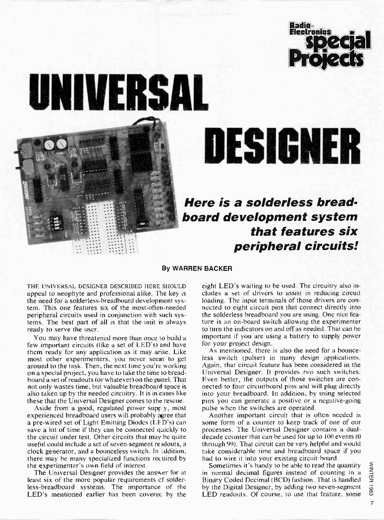
UNIVERSAL
DESIGNER
Here is a solderless bread- board development system
that features six peripheral circuits!
By WARREN BACKER
THE UNIVERSAL DESIGNER DESCRIBED HERE SHOULD appeal to neophyte and professional alike. The key is the need for a solderless-breadboard development sys- tem. This one features six of the most -often -needed peripheral circuits used in conjunction with such sys- tems. The best part of all is that the unit is always ready to serve the user.
You may have threatened more than once to build a few important circuits (like a set of LED's) and have them ready for any application as it may arise. Like most other experimenters, you never seem to get around to the task. Then, the next time you're working on a special project, you have to take the time to bread- board a set of readouts (or whatever) on the panel. That not only wastes time, but valuable breadboard space is also taken up by the needed circuitry. It is in cases like these that the Universal Designer comes to the rescue.
Aside from a good, regulated power supply, most experienced breadboard users will probably agree that a pre -wired set of Light Emitting Diodes (LED's) can save a lot of time if they can be connected quickly to the circuit under test. Other circuits that may be quite useful could include a set of seven -segment readouts, a clock generator, and a bounceless switch. In addition, there may be many specialized functions recuired by the experimenter's own field of interest.
The Universal Designer provides the answer for at least six of the more popular requirements cf solder - less -breadboard systems. The importance of the LED's mentioned earlier has been coverec by the
eight LED's waiting to be used. The circuitry also in- cludes a set of drivers to assist in reducing circuit loading. The input terminals of those drivers are con- nected to eight circuit pins that connect directly into the solderless breadboard you are using. One nice fea- ture is an on -board switch allowing the experimenter to turn the indicators on and off as needed. That can be important if you are using a battery to supply power for your project design.
As mentioned, there is also the need for a bounce - less switch (pulser) in many design applications. Again, that circuit feature has been considered in the Universal Designer. It provides , two such switches. Even better, the outputs of those switches are con- nected to four circuitboard pins and will plug directly into your breadboard. In addition, by using selected pins you can generate a positive or a negative -going pulse when the switches are operated.
Another important circuit that is often needed is some form of a counter to keep track of one of our processes. The Universal Designer contains a dual - decade counter that can be used for up to 100 events (0 through 99). That circuit can be very helpful and would take considerable time and breadboard space if you had to wire it into your existing circuit board.
Sometimes it's handy to be able to read the quantity in normal decimal figures instead of counting in a Binary Coded Decimal (BCD) fashion. That is handled by the Digital Designer, by adding two seven -segment LED readouts. Of course, to use that feature, some
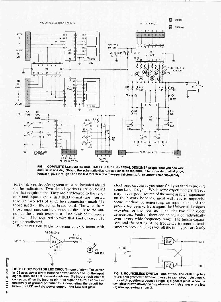
COUNTERS/DECODERS/READOUTS
LATCH
8
4
2
1
RESET
CP1
CPO
p 3 13
6 12
2 11
1 10
7 90 IC5 15
9368 14
16 80
o o 0 0 A
C
DI I
O`
O o c
O
O 0 0 0 O
0 0
GI I
0
0`,, 0 0 0 0
o FND500
A o o ( o
ci)
DIS2
1 4 2
0 8 IC 16 O
15 12 14 T 10' O O O C
O
CPO O 16
13 O 0 A
CP1 12 0 O O
o RESET IC4
9368 11 O O
O' 1 7 10 0 0 D O 0 2 1 90 0 E
4 O 2 15 O 0 o 8 6 14 O O G - -O
LATCH o 3 8C O FND 500
LED11 ú R1
DIS1
15062
St O-7 HIGH R5
1
S3 -a
14 12 o
4
80
11
0
S3 -b I
O C
S2 9 Ici 10 C D
13 7400 5O-1 S3 -c C
30 i 0 S3 -d
4 7 6
O
LOW O
BOUNCELESS SWITCHES
X X Y Y
LO HI LO HI
PULSER OUTPUTS
MONITOR SWITCH O
OFF O0N R
-- K
C S4
4R
1K
R3 1K
ó ó d A B C
SWITCH OUTPUTS
R2 1K
o
LEDI
R15 22062
LEDO =a
R21
100K
019 18K
MONITOR INPUTS
1 2 3 4 5 6 7 8
R16 R17 1.8K -t 1.8K
o
C1_.-.- Or."'
-o-K o o )F -o- Ca = Cb
D INPUTS
OUTPUTS
07 THRU R14 lJ 22011 EACH
LED8
018 22061
rr LED10
.t R20 >18K
-4100K
C2 ^ .01
CLOCK OUTPUTS
8 A
R22
FIG. 1. COMPLETE SCHEMATIC DIAGRAM FOR THE UNIVERSAL DESIGNER project that you can wire and use in one day. Should the schematic diagram appear to be too difficult to understand all at once, look at Figs. 2 through 8 and the text that describe these partial circuits. All doubts will clear up quickly.
sort of driver/decoder system must be included ahead of the indicators. Two decoder/drivers are on board for that requirement. They are hard -wired to the read- outs and input signals (in a BCD format) are inserted through two sets of solderless connectors much like those used on the actual breadboard. The wires from those input pins can be connected directly to the out- put of the circuit under test. Just think of the space that would be required to wire that kind of circuit to your breadboard.
Whenever you begin to design or experiment with
1/8 741:S240
INPUT
FIG. 2. LOGIC MONITOR LED CIRCUIT-one of eight. The driver in IC3 uses power direct from the power supply and not the input signal. Thus, the LED does not load down the input circuit when it comes on. When the input to pin 11 is high, the output at pin 9 is effectively at ground potential thus completing the circuit be- tween the LED and the power supply-the LED will glow.
D1 6V
+ PWR
electronic circuitry, you soon find you need to provide some kind of signal. While some experimenters already may have a good source of the most usable frequencies on their work benches, most will have to improvise some method of generating an input signal of the proper frequency. Here again the Universal Designer provides for the need as it includes two such clock generators. Each of them can be adjusted individually over a very wide frequency range. The timing capaci- tors and the setting of the frequency trimmer potenti- ometers provided gives you all the timing you are likely
HI
LO
FIG. 3. BOUNCELESS SWITCH-one of two. The 7400 chip has four NAND gates with two being used in each circuit. As shown, the switch position produces a high (1) signal at pin 3. When the switch is thrown down, the outputs reverse their states with a low (0) now appearing at pin 3.
8
to need. The frequency trimmers have about a 10:1 control over each of the two frequencies. Upper fre- quency limits are constrained by the normal Limitations associated with the 556 dual -timer integrated circuit used.
Finally, one circuit supplied by the Universal Designer is an on -board set of switches that are used to program logic levels required for various counters and gates, as well as many other circuits. The choice of either a logic "0" or "1" may be made by pressing a switch lever. A handy feature, indeed.
Other features include power -input pins that allow you to connect the Universal Designer directly to the main breadboard being used. Those pins are placed in a position where they will mate with the normal posi- tive and negative supply connections along the edge of most breadboard systems. In addition, if there is no such supply on the breadboard, the unit may be powered by a 6 -volt battery. In that event, the voltage is dropped through a diode on the Universal Designer and it can then supply power to the main breadboard pins.
For those readers who must scan the complete circuit diagram of a project in advance of the theory of opera- tion discussion, look at Fig. 1 now. However, partial diagrams illustrated in Figs. 2 through 8 coupled with the theory discussion makes life simpler for most read- ers. It is suggested that once the reader fully under- stands the operation of the circuit segments in each of the partial diagrams in Figs. 2 through 8, he should refer back to Fig. 1. Thus, the full versatility of the Universal Designer will become apparent in small doses.
Start to build your own Construction of the Universal Designer is quite
straightforward. Since no critical circuitry is involved, almost any kind of construction method can be used. However, a compact unit is built by using a small print- ed -circuit board. The Parts List at the end of this article includes the source for such a printed -circuit board, as well as a complete kit of parts.
The easiest way to put the Universal Designer together is by using a printed -circuit board. Either make one from the foil template shown in Fig. 9 from .0625 - in. single side board with 1 -ounce copper, or buy it made, cut, drilled and silk-screened with call outs added. The complete schematic diagram for the Uni- versal Designer is shown in Fig. 1 for those who wish to modify the circuit to their special needs. The board electrically connects to the solderless breadboard via a series of stake pins soldered to the board. Be sure these pins line up with the solderless board's mating holes. You may want to mount the board and solderless bread- board on a sloping surface, build a power supply, or add other improvements. It's all up to you.
Circuit description Each of the six functions provided by the Universal
Designer are generated by standard circuits. Let's take those functions in the same order as they were presented earlier in the article. The eight logic -monitor LED's can be broken down into one LED and its drive circuit (see Fig. 2). In reality, the driver is one section of a 74LS240 IC that houses eight identical drivers. That IC operates likes eight switches. When an input pin is provided a logic "0", it will produce a logic "1" at the output. Since a logic "1" is positive here, and
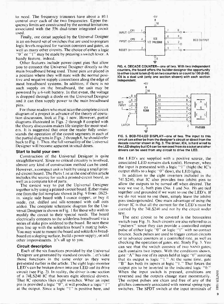
+5v
ICG
1/2 74LS390
1
BCD OUTPUT
FIG. 4. DECADE COUNTER-one of two. With two independent counters, the board offers the builder -designer the opportunity to either count to ten (0-9) on two counters or count to 100 (0-99). IC6 is a dual unit (only one section shown) with each section independent.
t -5V
r BCD INPUT
LATCH FN 0500
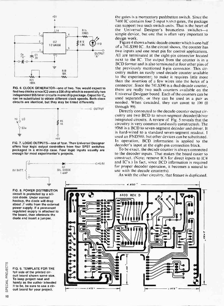
FIG. 5. BCD -TO -LED DISPLAY-one of two. The input to this circuit can either be from the designer's circuit or direct from the decade counter shown In Fig. 3. The driver, IC4, is hard wired to the LED display but IC4 can be removed from its socket and other drivers can be used from any circuit to drive the LED.
the LED's are supplied with a positive source, the associated LED remains dark (unlit). However, when the input is presented with a logic "1" (high) the IC's output shifts to a logic "0" (low), the LED lights.
In addition to the eight inverters included in the 74LS240, that IC also provides two inhibit pins to allow the outputs to be turned off when desired. The way we use it, both pins (No. 1 and No. 19) are tied together and grounded if we want to use the LED's. If we do not want to use them, simply leave the inhibit pins undergrounded. One main advantage of using the driver IC is that all the current for the LED's must be carried by the 74LS240 and not by the circuit under test.
The next circuit to be covered is the bounceless switch (see Fig. 3). Such circuits are also referred to as "pulsers" since they can provide a controlled output pulse of either logic "0" or logic "1" with no contact bounce. Such pulses are used to trigger certain circuits or to advance counters at a controlled rate, as well as checking the operation of gates, etc. Study Fig. 3. You can see that the switch consists of two NAND gates; each contains two inputs. With the conditions shown, gate "A" has one of its inputs held at logic "0" assuring that its output is logic "1." At the same time, gate "B" has both its inputs at logic "1." That forces the output pin to be inverted to the indicated logic "0." When the input switch is pressed, conditions are reversed and the outputs change state momentarily. The output pulses are clean and free of any of the glitches commonly associated with normal spring -type switches. The SPDT switch at the input terminals of
R21
100K
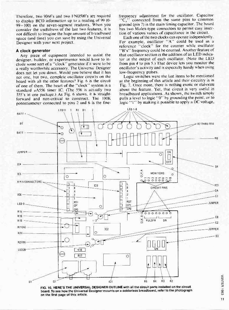
FIG. 6. CLOCK GENERATOR-one of two. You would expect to find two clocks since 1C2 uses a 556 chip which is essentially two independent 555 timer circuits in one chip package. Capacitor C2 can be substituted to obtain different clock speeds. Both clock circuits are identical, but they may be timed differently.
HI
t
LO R5
1K
S3 -a
ó +5V
O OUTPUT
FIG. 7. LOGIC OUTPUTS-one of four. Then Universal Designer offers four logic output controllers from four SPST switches packaged in a mini -dip case. Four logic inputs usually are enough for most experimenter's projects.
6V BATT. D1
SIL. DIODE 1 AMP
FIG. 8. POWER DISTRIBUTION circuit is protected by a sili- con diode. Under normal hookup, the diode will drop about .7 volts from the external power supply. If a permanent regulated supply is attached to the board, then eliminate the diode and insert a jumper.
FIG. 9. TEMPLATE FOR THE foil side of the printed cir- cuit board shown same size. To keep project neat and handy as the author intended it to be, be sure to use a cir- cuit board for your project.
-o +5.4V
the gates is a momentary pushbutton switch. Since the 7400 IC contains four 2 -input NAND gates, the package can support two such switch units. That is the heart of the Universal Designer's bounceless switches-a simple device, but one that is often very important to design work.
Figure 4 shows a basic decade counter which is one-half of a 74LS390 IC. As the circuit shows, the counter has two inputs and one reset pin for control applications. All are terminated at the eight -pin connector located next to the IC. The output from the counter is in a BCD format and is also terminated at four other pins of the previously mentioned 8 -pin connector. This cir- cuitry makes an easily used decade counter available to the experimenter; to make it requires little bore than the insertion of a few wires into the holes of a connector. Since the 74LS390 is a dual -decade counter, there are really two such counters available on the Universal Designer board. Each of the counters can be used separately, or they can be used as a pair as needed. When cascaded, they can count to 100 (0 through 99).
Directly connected to the decade -counter output cir- cuitry are two BCD to seven -segment decoder/driver integrated circuits. A review of Fig. 5 reveals that the circuitry is very common (and easily constructed). The 9368 is a BCD to seven -segment decoder and driver. It is hard -wired to a standard seven -segment readout. I used an FND500, but other devices can be substituted. In operation, BCD information is applied to the decoder's input at the eight -pin connection block.
To be exact, the decade counter is always connected to the decoder inputs. That makes the board easier to construct. (Note: remove IC6 for direct inputs to IC4 and IC's.) In fact, since BCD information is required for proper decoder operation, it becomes a natural to use with the decade counter(s).
As with the other circuitry, that feature is duplicated.
Therefore, two 9368's and two FND500's are required to display BCD information up to a reading of 99 (0-
99= 100) on the seven -segment readouts. When you consider the usefulness of the last two features, it is
not difficult to imagine the huge amount of breadboard space (and time) you can save by using the Universal Designer with your next project.
A clock generator Any piece of equipment intended to assist the
designer, builder, or experimenter would have to in- clude some sort of a "clock" generator if it were to be a really worthwhile accessory. The Universal Designer does not let you down. Would you believe that it has not one, but two, complete oscillator circuits on the board with all the other features? Fig. 6 is the circuit of one of them. The heart of the "clock" system is a standard eA556 timer IC. (The 556 is actually two 555's in one package.) As Fig. 6 shows, it is straight- forward and non -critical to construct. The 100K potentiometer connected to pins 2 and 6 is the fine-
BATT +
6V
BATT -
JUMPER
IC4
IC5
LED11 1 R1 D1
frequency adjustment for the oscillator. Capacitor "Ca" connected from the same pins to common ground (pin 7) is the main timing capacitor. The board has two Molex -type connectors to permit easy inser- tion of various values of capacitance in the circuit.
Each one of the two clocks can operate independently. For example, oscillator "A" could be used as a reference "clock" for the counter while oscillator "B's" frequency could be counted. Another feature of that oscillator section is the addition of an LED indica- tor at the output of each oscillator. (Note the LED from pin 4 to pin 5.) That device lets you monitor the oscillator's activity and is especially handy when using low -frequency pulses.
Logic switches were the last items to be mentioned at the beginning of this article and their circuitry is in
Fig. 7. Once more, there is nothing exotic or elaborate about the feature. Yet, that circuit is very useful in
breadboard applications. As shown, the switch simply pulls a level to logic "0" by grounding the point, or to logic "1" by making it possible to apply a DC voltage,
LED 1-8
8 PIN CONNECTORS
IC6
LED 9
R15
R16
R19
R21(A)
R20
R22(ß)
LED28
3 3 -3 3 3 3
L
8
4
2
1
RST
CP1
CPO
o
t1ì6
S1
R18
R17 1
IC2
o
8
4
2
1
RST
CP1
CPO
m
PULSER
J MONITORS
OFF
N ce a 11', co r co
Q O O 000 O
O
CIRCUIT PINS
0 0 0 0 0 0 0 I i
SW
ON
S2 IC1 R5 R4 R3 R2
FIG. 10. HERE'S THE UNIVERSAL DESIGNER OUTLINE with all the circuit parts installed on the circuit board. To see how the Universal Designer mounts on a solderless breadboard, refer to the photograph on the first page of this article.
R7 THRU R14
R6
S4
IC3
CA
Cl
JUMPER
CB
C2
JUMPER
S3
PARTS LIST
RESISTORS All resistors 1/4 -watt unless noted R1-150 ohms R2-R6-1000 ohms R7-R15, R18-220 ohms (see text) R16, R17-1800 ohms R19, R20-18,000 ohms R21. R22-100,000 ohms, trimmer potentiometers
CAPACITORS Cl, C2-.01 ceramic disc Ca. Cb-0.1 ceramic disc
2.2-4F electrolytic 22-4F electrolytic
SOLID-STATE DEVICES D1 -1A silicon diode DIS 1, DIS 2-FND-500 seven -segment displays I C 1-7400 IC2-556 IC3-74LS240 IC4, IC5-9368 or 4368 (see text) IC6-74LS390 LED1 thru LED11-red light emitting diodes
MISCELLANEOUS S1, S2-pusbutton switches, momentary contact, normally
open S3-4 position DIP switch S4-1 position DIP switch 8 -pin sockets (2)
16 -pin IC sockets (1) Small PC pins (20) PC sockets (4)
Alligator clips/insulators (2) 4-40 x We Nylon spacers (2)
4-40 x 1/4 Nylon spacers (2)
PC board (optional) Case, hardware, etc.
The following items are available from Etronix, 14803 NE 40th, Redmond, WA 98052.
6100 Kit $49.95 6100 Assembled $59.95 QT59B Breadboard
(2 required) $ 2.99 ea. QT59S Breadboard $12.50 ea.
PCB1 LEDI-LED11 DISP-1,2 U-3 U-4,5 U-6 R-21,22 S-1, S-2 S-3 S4 Misc
PARTS
$20.00 ea. .12 ea. .95 ea.
2.25 ea. 2.50 ea. 2.65 ea.
3386P -1-104100K Trimmer Pots .40 Pushbutton 1.20 JS -8750-04 4 Pos Dip Sw 1.60 JS -8750-01 1 Pos Dip Sw 1.25 Molx 0204-1112 Socket Pins .10 Moix 2202-2081 Strip Socket
(2 req'd) T46-4-9 Stake Pins (22 required)
6100 Printed Circuit Board L-72RD (10 Red LED's) FND500/503 (2 required) 74LS240 9368PC (2 required) 74LS390
ea. ea. ea. ea. ea.
.40 ea. .04 ea.
Please note that supplier's parts symbol designations vary slightly with those given in this article. For example: IC1 is supplier's U-1.
through a IK resistor, to the unit under test. Simple and effective, it will save both time and breadboard space. Four of those simple circuits are provided by the Universal Designer and are contained on an eight - pin mini -DIP switch unit.
Using the Universal Designer In use, the Designer is normally plugged into one
of the boards of your solderless-breadboard system. The power pins mate with the two rows of connectors along the edges of most breadboard systems. Use them to supply power to the breadboard if you use the battery -supply connections on the Universal Designer, or to transmit power to the Universal Designer if you
LED11
DIS1, DIS2
IC5
IC4
ICS
LED!
R21
R22
IC2
LED10
LEDI -LEDO
SI S2 ICI
THE UNIVERSAL DESIGNER looks like this after the last part is soldered into place. This photo duplicates Fig. 10 on the - pre vious page. Now fit the printed -circuit board onto a solderless breadboard and you are now set up to experiment with your next dream circuit.
take the power from the main system. If your system has other than standard power rows (such as the "Experimenter" series) then you will have to modify your board accordingly.
When connected as outlined, most of the major con- nections are then made between the breadboard and the Universal Designer through two rows of nine pins each. Of course, that means that the user will have four holes available in the breadboard for each of the eighteen pins to which he (or she) may connect wires to the circuit(s) being tested. Earlier, we mentioned that certain signals would be inserted through two eight -pin connectors on the board being discussed. That is still true and they will be used for input and output information relating to the decade counters and the seven -segment decoder/driver circuitry.
We said that batteries could be used to power the unit. Since TTL logic is based upon a 5 -volt supply, further mention of that circuit is in order. A convenient
(Continued on page 98) 12
TACHOMETER
This rapid -read analog -dial LED display lets you safely watch the road as you red -line the tach.
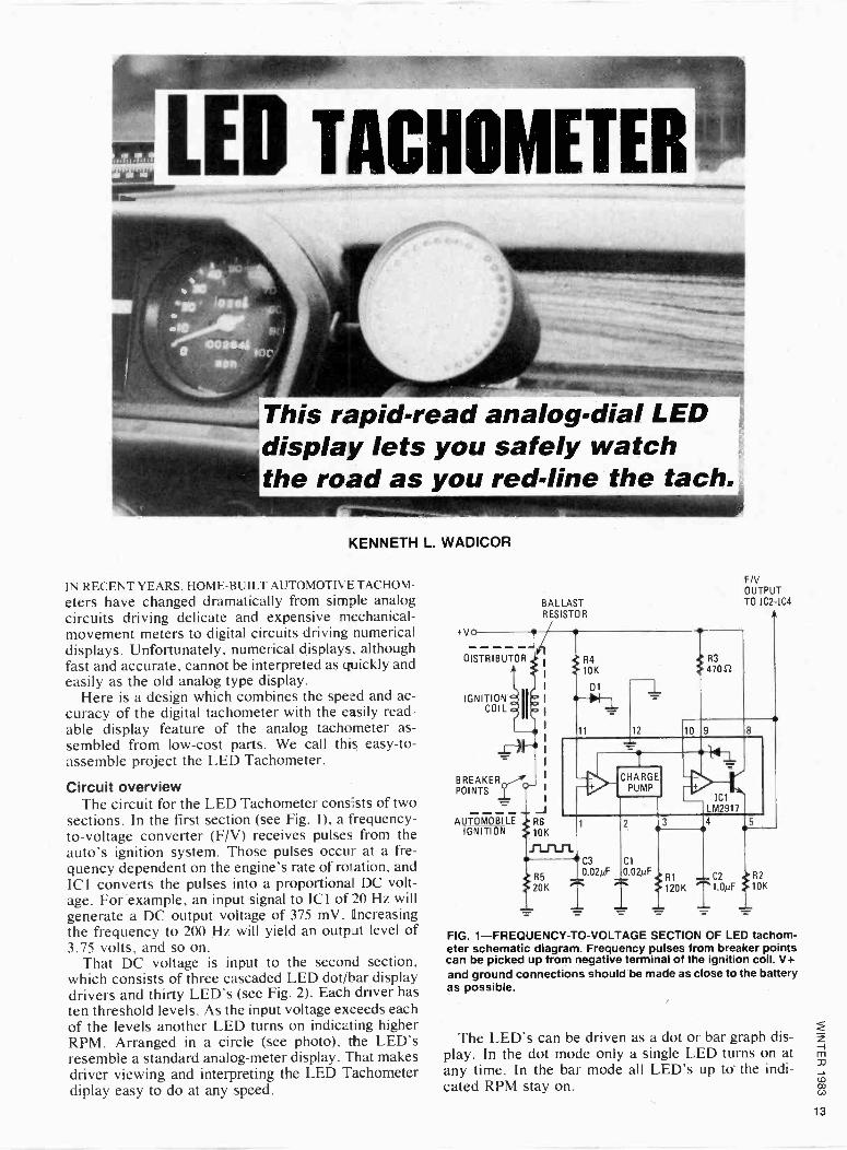
KENNETH L. WADICOR
IN RECENT YEARS, HOME -BUILT AUTOMOTIVE TACHOM-
eters have changed dramatically from simple analog circuits driving delicate and expensive mechanical - movement meters to digital circuits driving numerical displays. Unfortunately, numerical displays, although fast and accurate, cannot be interpreted as quickly and easily as the old analog type display.
Here is a design which combines the speed and ac- curacy of the digital tachometer with the easily read- able display feature of the analog tachometer as- sembled from low-cost parts. We call this easy -to - assemble project the LED Tachometer.
Circuit overview The circuit for the LED Tachometer consists of two
sections. In the first section (see Fig. 1), a frequency - to -voltage converter (F/V) receives pulses from the auto's ignition system. Those pulses occur at a fre- quency dependent on the engine's rate of rotation, and IC I converts the pulses into a proportional DC volt- age. For example, an input signal to ICI of 20 Hz will generate a DC output voltage of 375 mV. Increasing the frequency to 200 Hz will yield an output level of 3.75 volts, and so on.
That DC voltage is input to the second section, which consists of three cascaded LED dot/bar display drivers and thirty LED's (see Fig. 2). Each driver has ten threshold levels. As the input voltage exceeds each of the levels another LED turns on indicating higher RPM. Arranged in a circle (see photo), the LED's resemble a standard analog -meter display. That makes driver viewing and interpreting the LED Tachometer diplay easy to do at any speed.
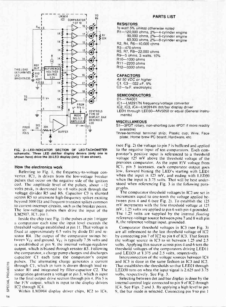
+Vo
BALLAST RESISTOR
F/V
OUTPUT TO 1C2-IC4
A
DISTRIBUTOR
l IGNITION
2 COIL
BREAKER POINTS
AUTOMOBILE IGNITION
J
R4 10K
D1 1 11 12
t R3
:fr 47052
10 9
CHARGE PUMP
IC1
LM2917
R6
10K
JLrl.rl
R5 20K
4
C3 Cl 0.02µF 0.02µF
SS R1 C2 R2
TT ?120K
T1.OhLF 4 10K
FIG. 1-FREQUENCY-TO-VOLTAGE SECTION OF LED tachom- eter schematic diagram. Frequency pulses from breaker points can be picked up from negative terminal of the ignition coil. V+ and ground connections should be made as close to the battery as possible.
The LED's can be driven as a dot or bar graph dis- play. In the dot mode only a single LED turns on at any time. In the bar mode all LED's up to the indi- cated RPM stay on.
I-
RHi 16
LM3914 1 TO
1C2 COMPARATORI R9
+D
to I ,,
10¢ Or. 11,1¡0
REF
THIS LOAD BOUT J7
DETERMINES RIO LED # 1 K
BRIGHTNESS a REFI - AJDJ,8
1K
1K
1K
1K
1 1K
REFERENCE VOLTAGE SOURCE
1.2V
1
T0_(ii> 3 V+
R9
1K
1K
1K
1K
1K
FROM SI
20K
IC 1 -
PIN 5 5
MODE SELECT
AMPLIFIER V- BUFFER
I
15$0I00
PARTS LIST
RESISTORS 1/2 -watt 5% unless otherwise noted R1-120,000 ohms, 2% -4 -cylinder engine
R7 90,000 ohms, 2% -6 -cylinder engine 22K 60,000 ohms, 2% -8 -cylinder engine
R2, R4, R6-10,000 ohms R3-470 ohms R5, R7, R8-22,000 ohms R9-5 ohms, 3 watts, 10% R10-1000 ohms R11-2200 ohms R12-3300 ohms
le
18 0f' I
0,e
O N FROM I
V+ PIN 11
CONTROLS 9 TYPE OF
2
DISPLAY, BAR OR SINGLE LED
FIG. 2-LED-INDICATOR SECTION OF LED -TACHOMETER schematic. Three LED dot/bar display drivers (only one is shown here) drive the 30 -LED display (only 10 are shown).
How the electronics work Referring to Fig. 1, the frequency -to -voltage con-
verter, ICI, is driven from the low -voltage breaker pulses that occur on the negative side of the ignition coil. The amplitude level of the pulses, about +12 volts peak, is decreased to +8 volts peak through the voltage divider R5 and R6. Capacitor C3 is shunted across R5 to attenuate high -frequency spikes existing beyond 1000 Hz and frequent transient spikes common to current -interrupt circuits, such as the breaker points. The low -voltage pulses then drive the input of the LM2917, ICI, pin l .
Inside the chip (see Fig. 1) the pulses at pin 1 trigger a comparator each time the input level exceeds the threshold voltage established at pin 11. That voltage is fixed at approximately 0.5 volts by diode D1 and re- sistor R4. The output of the comparator swings be- tween Vcc and ground. Vcc is typically 7.56 volts and is established at pin 9, the internal voltage -regulator output, which is biased through resistor R3. Following the comparator, a charge pump charges and discharges capacitor C 1 each time the comparator's output pulses. The alternating charge generates a current through Cl, which in turn is driven through load re- sistor R1 and integrated by filter -capacitor C2. The integration generates a voltage at pin 3, which is input to the final output drive section through pin 4. Pin 5 is the F/V output, which is input to the display drivers IC2 through IC4.
Within LM3914 display driver chips, IC2 to IC4,
CAPACITORS All 50 VDC or higher Cl, C3-.022µF, 5% C2-1µ F, electrolytic
SEMICONDUCTORS D1 -1N4001 IC1-LM2917N frequency/voltage converter IC2, IC3, IC4-LM3914N dot/bar display driver LED1 through LED30-MV5050 or equal (General Instru-
ments)
MISCELLANEOUS S1-3PDT rotary, non -shorting (use 4PDT if more readily
available) Three -terminal terminal strip; Plastic cup; Wire; Face
plate; Home brew PC board; Hardware, etc.
(see Fig. 2) the voltage to pin 5 is buffered and applied to the negative input of ten comparators. Each com- parator's positive input is referenced to a threshold voltage 125 mV above the threshold voltage of the previous comparator. As the input F/V voltage from ICI, pin 5 increases, each comparator output goes low, forward biasing the LED's starting with LEDI when the input is 125 mV, and ending with LED30 when the input is 3.75 volts. That will be best under- stood when referencing Fig. 3 in the following para- graphs.
The comparator threshold voltages in IC2 are set in increments equal to one -tenth the voltage applied be- tween pins 4 and 6 (see Fig. 2). To establish the 125 mV increments with the first threshold voltage at 125 mV, 1.25 volts are applied to pin 6 with pin 4 grounded. The 1.25 volts are supplied by the internal floating reference -voltage source between pins 7 and 8 with pin 8, the reference voltage input, grounded.
Comparator threshold voltages in IC3 (see Fig. 3) are all referenced to the last threshold voltage of IC2 by connecting pin 7 of IC2 to pin 8 of IC3. That forces the voltage source in IC3 to sit between 1.25 and 2.5 volts. Applying this source across pins 4 and 6 sets the threshold voltages of the comparators driving LED11 and LED20 at 1.375 and 2.5 volts, respectively.
Interconnection of the voltage sources between IC4 and IC3 is done in the same fashion as IC3 and IC2. That establishes the thresholds so that LED21 through LED30 turn on when the input signal is 2.625 and 3.75 volts, respectively. See Fig. 3.
Selecting between dot and bar display is done by the internal -control logic connected to pin 9 of IC2 through IC4. See Figs. 2 and 3. By applying a high level to pin 9, the bar mode is selected. Connecting pin 9 to pin 1
LM2917 FREQUENCY TO VOLTAGE CONVERTER
R3,470
R4, 10K
1N4001 01 1
R2 9 6 - 10K
10 5 N + C2, 1µF
11 IC1 4 R1, 120K
13 2 Cl .022µF+-i_
14 1
R6 we
C3 R5 10K .022µF T 22K
HIGH VOLTAGE PULSES
LOW -VOLTAGE BREAKER PULSES
-lJ-LrL BREAKER
GNDI
BALLAST RESISTOR
IGNITION COIL
1-)
CONOENSOR
V+ LEO
DISTRIBUTOR
V+ BATTERY
BREAKER POINTS
AUTO IGNITION
LED 1 e) E) e) Occ
0O O !) E) 18 17 16 15 14 13
IC2 LM3914
1 2 3 4 5 6
12 11 10
7 8 9
R7
22K
LED 11
51
DOT
2
3BAR
E)
E) 18 17 16 15 14 13 12 11 10
IC LM3914
2 3 4 5 6 7 8 9
22 R8K
1 LED 21
Si 5 DOT
E)
E) 18 17 16
V1N
15 14 13 12 11 10
IC4
LM3914
60 BAR
1 2 3 4 5 a
R10 / 1K = _j_
8 9
R9 5n
(3 WATTS)
LED 30
51
8 DOT
7 90 BAR
R12 / 3.3K-/
R 19VS1 2.2K J
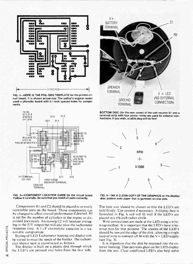
FIG. 3-FULL SCHEMATIC OF THE TACHOMETER. Except for terminals, switch S1, resistor R9, and the LED's, all components mount on a printed -circuit board.
of each following display driver and connecting pin 9
to pin 11 on the last display driver converts the display to dot mode.
Resistors R10 through R12 control the LED bright- ness. The current drawn from each internal voltage source at pin 7 by the resistors determines the bright- ness of the 10 LED's run by that particular voltage source. The current through the resistors is approxi- mately one tenth of the current through the LED's. Current -limiting is provided in the LM3914 chip to protect the LED's. Resistor R9 has been included to decrease heating of the drivers during the bar -mode operation.
Setting the F/V constant The frequency -to -voltage conversion constant de-
termines the output voltage from the F/V chip, IC 1,
for a given input frequency. See Figs. 1 and 3. That constant is set by components R1 and C 1 so that an input frequency of 200 Hz yields an output DC level of 3.75 volts. The conversion constant is 3.75 volts divided by 200 Hz, which equals .019 volts per Hz.
The values of R1 (120K) and Cl (0.022µf) have been chosen so that 6000 RPM from a four -cylinder engine yields a full scale reading on the display. R1 is de- creased to 90K or 60K ohms for six- or eight -cylinder engines, respectively.
The distributors frequency input pulses to the F/V chip ICI is calculated by the following equation:
Freq = RPM x (No. of cylinders)/120.
Thus, an eight -cylinder car at 600 RPM mile speed will produce 40 pulses per second.
LED .. . Cl C3
R6 (1 of 30)
IC4
R12
O V+
R5
R1
IC1
D1
% R4 . R3
R2
IC2
R7
READY FOR ASSEMBLY, the circuit board and display disc are about to be slid into the plastic -cup housing. Note that the author chose to solder wires to the LED leads. Wire -wrapping is just as good. Also, you may elect to use rainbow -type flat ribbon cable to interconnect the LED drivers to the LED's.
Construction A printed -circuit board layout and parts -placement
diagram are shown in Figs. 4 and 5. The circuit isn't sensitive to layout so any method of construction can be used.
3 INCHES
FIG. 4-HERE IS THE FOIL -SIDE TEMPLATE for the printed -cir- cuit board. It is shown actual size. The author's original model used a phenolic board with 0.1 -inch spaced holes for compo- nents.
TO R9, S1-3, S1-6 AND S1-9 (V+ LED)
-R7- 10 LEADS TO LED 110
PINS 10-18 AND PIN 1
JUMPER+
51-5 51-2
"111 gADS TO LED 11-20 PINS 10-18 AND PIN 1
J-R8_
-R3- -R2 C2
-V- 10 LEADS TO LED 21-30,
_O1- -R1 C1
Ú PINS 10-18
-R6- AND P1
-R5_ C3
V+ TERMINAL S1-7
(12 VDC) INPUT FROM BREAKER TERMINAL
GROUND TERMINAL
S1-8
FIG. 5-COMPONENT-LOCATION GUIDE for the circuit board. Follow it carefully. Be sure that you insert all parts correctly.
Components R 1 and C2 should be placed in an easily accessible area on the board. Those components can be changed to affect overall performance if desired. RI is set for the number of cylinders in the engine as dis- cussed previously. Increasing C2 will increase averag- ing in the F/V output but will also slow the tachometer response time. A 1 N F electrolytic capacitor is a rea- sonable compromise.
Styling of LED Tachometer housing and display can be varied to meet the needs of the builder. The tachom- eter shown here is constructed as follows.
The display is built on a plastic disk through which the LED's are pressed into holes from the rear side.
v+ BATTERY
TERMINAL
BREAKER
TERMINAL
GROUND
TERMINAL
R9
V + LED
(NO EXTERNAL
CONNECTION)
BOTTOM DISC (for the rear cover) of the unit mounts S1 and a terminal strip with four posts-three are used for external con- nections. If you wish, a cable plug will do fine!
1
I / 3
RPM
X1000
4
5
FIG. 6-INK A CLEAN COPY OF THE GRAPHICS on the display - disc pattern onto paper that is gummed on one side.
The hole size should be chosen so that the LED's are held firmly. Use cement if necessary. A display face is furnished in Fig. 6 and will fit well if the LED's are placed in a 1% inch radius circle.
Wire connections are made at the LED using a wire - wrap method. It is important that the LED's have wire - wrap pins for that purpose. The anodes of the LED's should be toward the edge of the disk, allowing a single loop of wire to connect all 30 with the V+ LED supply (see Fig. 3).
It is important that the disk be recessed into the ex- terior housing. That prevents glare on the LED display from the sun. Clear undiffused LED's also help solve
LED (1 OF 30)
EXTERIOR HOUSING (PLASTIC CUP)
3 _11111111
DOT/BAR SELECTOR
BOTTOM DISK
BREAKER, V+ AND GROUND TERMINALS
SCREW
SCREW (COUNTER SUNK)
PLASTIC ROD
(SIDE VIEW) L BRACKET (NOT TO SCALE)
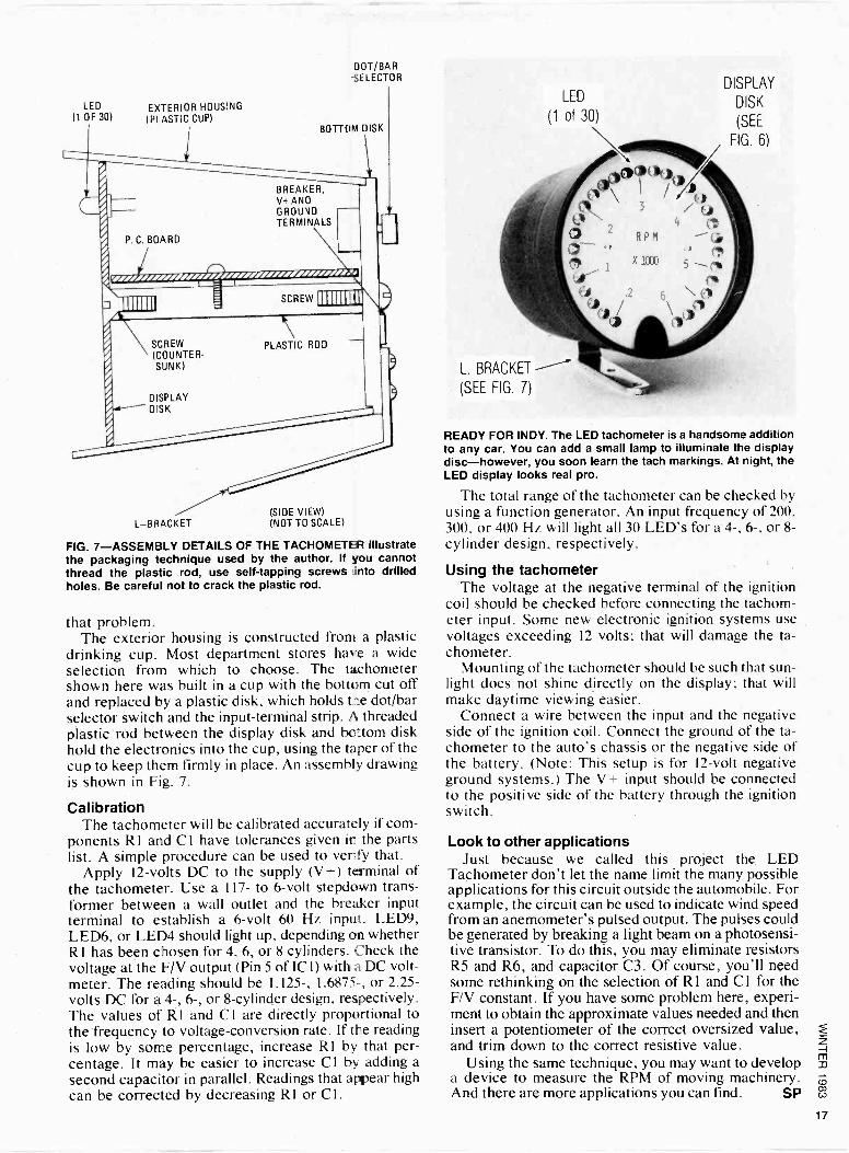
FIG. 7-ASSEMBLY DETAILS OF THE TACHOMETER illustrate the packaging technique used by the author. If you cannot thread the plastic rod, use self -tapping screws nto drilled holes. Be careful not to crack the plastic rod.
that problem. The exterior housing is constructed from a plastic
drinking cup. Most department stores have a wide selection from which to choose. The tachometer shown here was built in a cup with the bottom cut off and replaced by a plastic disk, which holds the dot/bar selector switch and the input -terminal strip. A threaded plastic rod between the display disk and bottom disk hold the electronics into the cup, using the taper of the cup to keep them firmly in place. An assembly drawing is shown in Fig. 7.
Calibration The tachometer will be calibrated accurately if com-
ponents R1 and CI have tolerances given in the parts list. A simple procedure can be used to verify that.
Apply 12 -volts DC to the supply (V+) terminal of the tachometer. Use a 117- to 6 -volt stepdown trans- former between a wall outlet and the breaker input terminal to establish a 6 -volt 60 Hz input. LED9, LED6, or LED4 should light up, depending on Whether R 1 has been chosen for 4, 6, or 8 cylinders. Check the voltage at the F/V output (Pin 5 of ICI) with a DC volt- meter. The reading should be 1.125-, 1.6875-, or 2.25 - volts DC for a 4-, 6-, or 8 -cylinder design, respectively. The values of R l and Cl are directly proportional to the frequency to voltage -conversion rate. If the reading is low by some percentage, increase R1 by that per- centage. It may be easier to increase C 1 by adding a second capacitor in parallel. Readings that appear high can be corrected by decreasing R1 or Cl.
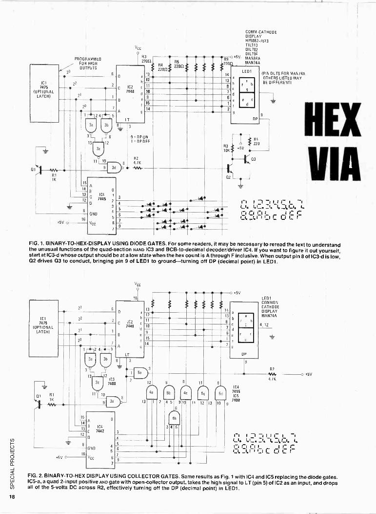
LED
(1 of 30)
L. BRACKET
(SEE FIG. 7)
DISPLAY
DISK
(SEE
FIG. 6)
READY FOR INDY. The LED tachometer is a handsome addition to any car. You can add a small lamp to illuminate the display disc-however, you soon learn the tach markings. At night, the LED display looks real pro.
The total range of the tachometer can be checked by using a function generator. An input frequency of 200, 300, or 400 Hz will light all 30 LED's for a 4-, 6-, or 8 - cylinder design, respectively.
Using the tachometer The voltage at the negative terminal of the ignition
coil should be checked before connecting the tachom- eter input. Some new electronic ignition systems use voltages exceeding 12 volts; that will damage the ta- chometer.
Mounting of the tachometer should be such that sun- light does not shine directly on the display; that will make daytime viewing easier.
Connect a wire between the input and the negative side of the ignition coil. Connect the ground of the ta- chometer to the auto's chassis or the negative side of the battery. (Note: This setup is for 12 -volt negative ground systems.) The V+ input should be connected to the positive side of the battery through the ignition switch.
Look to other applications Just because we called this project the LED
Tachometer don't let the name limit the many possible applications for this circuit outside the automobile. For example, the circuit can be used to indicate wind speed from an anemometer's pulsed output. The pulses could be generated by breaking a light beam on a photosensi- tive transistor. To do this, you may eliminate resistors R5 and R6, and capacitor C3. Of course, you'll need some rethinking on the selection of RI and CI for the F/V constant. If you have some problem here, experi- ment to obtain the approximate values needed and then insert a potentiometer of the correct oversized value, and trim down to the correct resistive value.
Using the same technique, you may want to develop a device to measure the RPM of moving machinery. And there are more applications you can find. SP
&
IC1
7475 (OPTIONAL
LATCH)
PROGRAMMED HIGH
OUTPUTS 23
vcc
22 2
21 1
20 7
Q1
1r -j2
3a
13
4,J
3c
5
3b
12
R3
22052 3 * 13 í
C IC2 c
7448
B e
A g
LT
R9
2 122052
14
12 13
11
10
9 6
15 1
14 2
81 3
O=DPON 1=0POFF
R2 4.7K
9 3d 1/A,
15
14
13 6
12
J_ - 8
+5V o 16
GND
VCC
IC4 7445
0
1
4
5
6
R3
10K
+5V,
a
d
e
9
COMM-CATHODE DISPLAY HP5082-7613 TIL313 DIL 702 DIL704 MAN84A MAN74A
LEDI
a
f b
e c
d
(PIN OUTS FOR MAN74A OTHERS LISTED MAY BE DIFFERENT)
9
DP
+5V
R4
220
Q21 I
6
7
v ^ rme' -ai- +
Q
ri I -1 -I I_I Ì 1 -1 L 1. 1.1_. _1. 1. _ 1 1 I ri I 1- r 1_` _ I I'_I r LI I_ 1-
HEX
VIA
FIG. 1. BINARY -TO -HEX -DISPLAY USING DIODE GATES. For some readers, it may be necessary to reread the text to understand the unusual functions of the quad -section NAND IC3 and BCB-to-decimal decoder/driver IC4. If you want to figure it out yourself, start at IC3-d whose output should be at a low state when the hex count is A through F inclusive. When output pin 8 of IC3-d is low, 02 drives 03 to conduct, bringing pin 9 of LED1 to ground-turning off DP (decimal point) in LED1.
ICI 7475
(OPTIONAL LATCH)
+5V 0 C
12 IC3
7400
7
vcc o
16
5h
2 4 5 9 10 11
6
3 45
11 8 1 / 4c 5c 5d
0 +5V
9
IC4 7415 IC5
7409 9
LED1 COMMON CATHODE DISPLAY MAN74A
4 12
1
R2
4.7K
I-I I 1 -_I II 1 1 -1 L.1. 1.'_. _1. _1.I_1. I. 1-1 1_I r 1 1 _'c'
I I '_I r LI 1_ I
o +5V
FIG. 2. BINARY -TO -HEX DISPLAY USING COLLECTOR GATES. Same results as Fig. 1 with IC4 and IC5 replacing the diode gates. IC5-a, a quad 2 -input positive AND gate with open -collector output, takes the high signal to LT (pin 5) of IC2 as an input, and drops all of the 5 -volts DC across R2, effectively turning off the DP (decimal point) in LED1.

BINARY TO
DISPLAY
THE
JUNK BOX What may be junk to many represents a wealth of theory and a practical hex display
D.E. PATRICK
USING INEXPENSIVE SEVEN -SEGMENT DISPLAY LED'S AND SOME
logic (mental and TTL) you can make sense out of a micro- processor's front panel, ease debugging procedures, or pro- vide an alternative to some expensive monolithic binary to hexadecimal (hex) displays. All this can be accomplished for only a few dollars. Even less, if you own the LED displays. The TTL circuits presented are recommended only if you have the parts in your junk box.
From the junk box-only The circuits in Figs. 1 and 2 may be primitive, but they
might represent your cheapest out, if you have an abundance of TTL junk. Operation is similar, with one using diode gates, while the other uses open -collector AND gates.
In either case, to prevent any user -perception errors in
reading the LED's, the right-hand decimal point (DP) is lit
for all numerals 0 thru 9, while during hex alpha A -B -C -D -E - F readout, represented as A -b -c -d -E -F, the decimal point is
out. The DP is used in this display configuration to eliminate any confusion, which might otherwise take place, between the numbers 6 and hex alpha b-they would be identical otherwise.
An optional 7475 latch, IC 1, allows the use of active low
or high input signals by programming its Q and Q outputs. At the same time, it provides the ability to latch input signals. But, when deleted, active high -input signals are required.
For active binary high -input signals to IC2, a 7448 BCD - to -seven -segment decoder driver, with active high outputs, decimal 0 through 9 or binary 0000 through 1001 are dis- played normally. The DP is also lit via IC3 for all numerals. When the input of IC2 exceeds decimal 9 or binary 1001, the lamp test (LT) input to IC2 is activated by being brought low
via IC3, extinguishing the DP and forcing the outputs of IC2 to an active high state. If nothing else happened for hex inputs of A through F there would appear a numeral "8" or LED1 with the DP extinguished-read on.
Looking at the operation of IC3, the NAND gates IC3-a and IC3-b are inputed with B and C inputs of IC2 which represents 2' and 22, respectively. See Fig. 1 or 2. Both IC3-a and IC3-b receive low inputs at the same time when,8 and 9 binary numerals are received with both outputs going high, and inputting to IC3-c. This results in a low signal supplied to IC3-d, pin 10, which will have a high output no
matter what the input on pin 9 of IC3-d might be. It just so
happens that pin 9 is driven high by bus D (23 signal to pin 6
of IC2), but the output of IC3-d remains high as stated before. When A through F are hex outputs from ICI, and D
bus (23) is always high, and the paired B and C buses are never both high at the same time. Thus the output of IC3-d is
always high for alpha characters, and those coincide with the high D bus to drive IC3-d to a low, or ground. Under these conditions, the light test (LT, pin 3 on LC2) goes low, turns off the DP, and lights up all segments (a through g of LED 1)
displaying an "8" as mentioned earlier. Ground is applied to IC4 a 7445 BCD to decimal decoder
driver in Fig. 1 or a 7442 decoder in Fig. 2, with active low outputs. When D goes high on IC2, Ql conducts and drives pin 4 on IC4 to ground. IC4 decodes the three Least Signifi- cant Bits (LSB's), A, B, and C, while its D input is tied to
ground. But, the decimal 0 and 1 outputs are not used, so
albeit ground is applied when D goes high (a decimal number 8) IC4 effectively performs no operation for 1000 or 1001
binary inputs. The outputs of IC4 feed a series of diode gates in Fig. 1 and open collector AND gates in Fig. 2. In either case, the gates act to turn off unwanted segments in the diplay to form the necessary alpha characters.
For example, consider a 1010 binary input, or hex A. IC4 sees only the LSB's 010 or a decimal 2. The decimal 2 is
outputted from IC4 as a active low signal and turns off the d segment of LED1 in Figs. 1 and 2. Thus the character A is
formed, with segments e -f -a -b -c -g still remaining lit. Next, consider a binary 1011 input. IC4 sees only the LSB's 011 or a decimal 3. The decimal 3 is outputted and turns off the a and b segments; thus, the character b is formed. And the remaining characters c -d -E -F are formed in like manner.
The 220 -ohm pullup resistors R3 -R9 used across the out- put lines of the 7448 driver has the net effect of controlling brightness, and the lower the value of those pullup resistors, the brighter the display, but do not exceed the limitations of the LED devices used.
Finally, a large number of TTL or equivalent gate combos and/or logic families might be used to accomplish the same end. Unless you have the parts shown on hand, it would hardly be worth while purchasing them new. Admittedly, using the parts discussed in this article is similar to a trip down TTL memory lane. Nevertheless, you'll be pleasantly surprised by the dollar savings-an experience that should happen every day. SP
DISCO LICHT
ORGAN CONTROL
ADD EXTRA EXCITEMENT TO ANY MUSICAL ENVIRONMENT AND make an invaluable addition to any game or party room with the Disco Light Organ Control. The device uses an external music source to switch three separate strings of colored lights on and off in tempo to the music played. The device creates an exciting effect of multi -colored lights dancing to music.
Circuit operation The complete schematic diagram of the Disco Light Organ
Control is shown in Fig. 1. An external music source is applied to the primary winding of audio transformer T l . The audio signal from the transformer is coupled through the master control potentiometer R10 and capacitor C I , to the audio amplifier Q1. The amplified audio signal from Q1 is coupled to three light -switching circuits. Each light - switching circuit is activated by a different range of audio frequencies, which is primarily determined by the capacitors C4, C5 and C6, and C7. The light -switching circuits contain SCR's which are activated by the high, medium, and low audio frequencies. Potentiometers R11 and Rl2 control the amount of input voltage needed to "fire" the gate of their corresponding SCR. When an SCR fires, it applies 117 -volts AC across its respective socket and simultaneously lights the
BARRY L. THOMPSON
light string plugged into that socket to the tempo of the music supplied to the Disco Light Organ control.
Neon light NE4 glows when the Disco Light Organ Con- trol is switched on. Neon lights NEI , NE2, and NE3 are used
REAR VIEW OF THE ORGAN shows the non -polarized output s ckets that you may want to replace with 3 -prong units. Your model should have the fuse holder showing from this view.
20
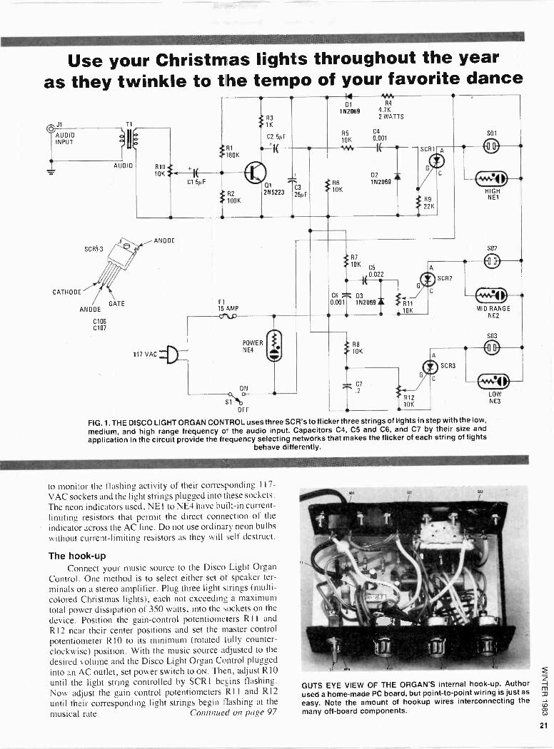
Use your Christmas lights throughout the year as they twinkle to the tempo of your favorite dance
sJ1 AUDIO INPUT
CATHODE
AUDIO
ANODE
C106 C107
+ R10.e IE 10K
Cl 5µF
1R11 80K
R2
100K
R3
1K
__
C R5 C4
2 5µF 10K 0.001
JJ l (
mIlkm
(11 C3 2N5223 25µF
D1 R4
1N2069 4.7K 2 WATTS
R6
10K
1N2069 D2 4
S01
SCR1 A ¡,
R9
22K
ANODE
117 VAC 4.) --
F1
15 AMP
cr D
POWER NE4
ON q o
OFF
R7 } 10K C5
6-1(0.022 C6 i^ 03
0.001 1N2069 =
l R8
4 10K
R11
10K
HIGH NEI
S02
- C7
I.2 * R12 10K
A
SCR2
C
MID RANGE N E2
A
C
SCR3
S03
FIG. 1. THE DISCO LIGHT ORGAN CONTROL uses three SCR's to flicker three strings of lights in step with the low,
medium, and high range frequency of the audio input. Capacitors C4, C5 and C6, and C7 by their size and
application in the circuit provide the frequency selecting networks that makes the flicker of each string of lights behave differently.
to monitor the flashing activity of their corresponding 1 17 -
VAC sockets and the light strings plugged into these sockets.
The neon indicators used, NE l to NE4 have built-in current -
limiting resistors that permit the direct connection of the
indicator across the AC line. Do not use ordinary neon bulbs
without current -limiting resistors as they will self destruct.
The hook-up Connect your music source to the Disco Light Organ
Control. One method is to select either set of speaker ter-
minals on a stereo amplifier. Plug three light strings (multi- colored Christmas lights), each not exceeding a maximum total power dissipation of 350 watts, into the sockets on the
device. Position the gain -control potentiometers Rl I and
R I2 near their center positions and set the master control potentiometer R 10 to its minimum (rotated fully counter-
clockwise) position. With the music source adjusted to the
desired volume and the Disco Light Organ Control plugged
into an AC outlet, set power switch to ON. Then, adjust R10
until the light string controlled by SCR 1 begins flashing. Now adjust the gain control potentiometers R 1 1 and R12
until their corresponding light strings begin lashing at the
musical rate. Continued on page 97
LOW NE3
GUTS EYE VIEW OF THE ORGAN'S internal hook-up. Author used a home-made PC board, but point-to-point wiring is just as
easy. Note the amount of hookup wires interconnecting the many off -board components.
1. l
COMPUTER GAMES ARE FUN. THEY ARE EVEN MORE FUN WHEN you can hear the zap and zizzle of laser cannons destroying the Galaxian Invaders; or the bonk-boiiinnng of computer - simulated pinball; or the electronic xylophone melodies of a Dancing Demon.
If a computer game has sound effects (some are silent), the audio signal is available at the output port for the cassette data -storage system. Depending on the particular computer you have, the output level from the cassette interface will be either "line level" for connection to the recorder's AUX input, or "microphone level" for connection the the record- er's MJcRO(phone) input. Either way, just connect any hi -Z input amplifier (such as the CompuSound) to the cassette - interface output and you'll get true-to-life sound effects.
CompuSound's hi -Z input impedance allows it to be con- nected directly across the computer's output to the cassette recorder and left permanently connected to the line, without affecting data or program dumps to the cassette. If you go from programming to games and want sound, all you need to do is turn on the CompuSound's power. You don't have to juggle patch -cord interconnections between the computer, the amplifier, and the cassette recorder.
Though the CompuSound was designed specifically for the Radio Shack TRS-80 computer, it should work with any computer's cassette interface output. If the game you use has sound effects through your computer's cassette port, the CompuSound should do the job.
How it works The CompuSound is a line -powered amplifier with about
20 dB of gain. The input -circuit has two jacks, J1 and J2, which allow the CompuSound to be "bridged" across the computer's output to the cassette recorder without need to splice into the computer/recorder cable (See Fig. 1.) You plug the connector from the computer into either jack and use a small patch cord from the remaining jack to the recorder.
All amplifier stages, everything from the preamplifier input to the power -amplifier output, is contained in a re- latively inexpensive integrated circuit, the LM386, which will work off a power source in the range of about 4-12 volts DC. While the CompuSound's volume level won't wake up your neighbors in the middle of the night, or disturb the landlord, it's enough to add a new dimension of excitement to computer games. Essentially, the maximum volume level is about that of a good pocket transistor radio: 400 mW at 8 ohms input.
The amplifier uses a minimum of parts and very little is critical. To reduce the possibility of self -oscillation, capaci- tor Cl, the high -frequency power -supply by-pass, should be installed as close as possible to ICI's power -supply terminal, pin 6. And resistor R3 and capacitor C2, the output high - frequency "filter" , should similarly be close to IC 1. In short, keep the leads of Cl, C2, and R3 as short as possible.
Maximum output power with a power supply in the 6-12 volt range will be attained with an 8 -ohm speaker. However, if you have one of the older 3.2 ohm or 4 ohm replacement speakers lying around the shop by all means use it.
Tone tuning The low -frequency response is determined by output-
CompuSound Add spaced -out sound to your computer games by adding this tiny project to your computer's cassette interface.
HERB FRIEDMAN
CompuSound
e
e
pOwER
VOLUME
22
FIG. 1. COMPUSOUND SCHEMATIC DIAGRAM is as easy to look at as it is to assemble on a printed -circuit board. P.
capacitor C3's value, which limits the low -frequency re-
sponse to a level that can be safely handled by 21/2- to 4 -inch speakers. If you make C3 larger for a "bigger bass" you can damage a small speaker. Actually, the frequency range is
more than adequate for electronic -game sound effects. The peak current drain at maximum volume for an 8 -9 -volt
power source is nominally 100 mA. Quiescent current drain is about 10 mA. The current drain is just a little too much for a
standard transistor -radio 9 -volt battery. An alkaline battery would work welt but it would not have an extended life. A few lengthy galactic invasions, or a long session of pinball, and a battery will be too pooped to zizzle, let alone zap.
Building it
The unit shown in the photos is built in a plastic utility box approximately 33/4 x 2 x 61/4 inches, having pre -drilled holes for a speaker grille. It is available from several mail- order parts houses, as well as from local parts distributors. If you can't get a pre -drilled cabinet, use a standard plastic cabinet and drill your own speaker grille. You're not in-
terested in "hi -f -i", so a handful of 3/16 -inch or'/4-inch holes should do the trick.
A 31/2 -inch speaker produces adequate electronics sound - effects of good quality, and fits nicely into the cabinet. Smaller speakers, such as the 2 -inch and 21/2 -inch, produce a
thin sound that lacks body, so use the larger speaker if possible. Don't worry if it has no mounting flanges. You can cement the speaker to the cabinet by applying a thin layer of contact adhesive or "airplane cement" around the rim of the speaker. Allow 24 hours for the cement to dry thoroughly.
The PC Board The amplifier is assembled on a small printed -circuit board
that measures approximately 31 x 29/16 inches. Make any adjustments to the overall shape of the board required to fit the specific cabinet you use. Similarly, if necessary, modify the PC -foil layout to accommodate the components you use.
When you make the PC board (see Fig. 2), keep in mind that volume -control R2 is installed on the foil side of the board; it actually carries (supports) the PC board. The three potentiometer terminals pass through the board from the foil side and are tack -soldered to the foil(s). To take the support load off the terminals, R3's case is tack -soldered to any foil passing from under the potentiometer's case on the approx- imate opposide side of the terminals. Don't overdo the sup- port; the terminals and one foil -to -case solder connection are
enough to support the PC board, even with power transfor- mer Ti installed. To protect the LED used as a power in-
dicator, and to prevent the, PC board from bending, place a
1/2 -inch standoff on the foil side of the board at one transfor- mer mounting screw. If you don't have a standoff, simply use one oversize mounting screw at Ti and cut it short so approx- imately 1/2 inch protrudes through the board.
You may select potentiometer R2 with or without a SPST switch (S1 in Fig. 3) to control the power supply. If you decide to go with the integrated unit, be sure there is enough height in the box to clear the part. You may insert S 1 into the AC power cord by using a typical lamp -cord switch.
BR1, a diode bridge assembly, might have only the posi- tive (+) terminal marked, or both the positive (+) and negative (-) terminals marked. Make certain you position BR1 correctly on the PC board. Check the peg board package
v--o-- J1
R1
47K
J2
117 VAC
6.3 VAC
C
IC1 TOP VIEW LM386
LM386
Cl 1 T
R4
5600
TC4 1000
C3 220 SP1
,R3 1052
C2
.05
r/v LED 1
PARTS LIST Resistors 1/2 or 1/4 watt, 10% unless otherwise noted. R1-47,000 ohms R2-25,000 to 100,000 ohms, audio taper potentiometer with
switch S1 (see text) R3-10 ohms R4 -56O ohms
Capacitors rated 10 WVDC or higher C1-0.1 µF Mylar or disk C2-0.05 µF Mylar or disk C3 -22O to 250 µF electrolytic C4-1000 µF electrolytic
Semiconductors BR1-Integrated DIP bridge rectifier, 25 PIV or higher IC1-LM386 integrated circuit audio amplifier LED1-Light-emitting diode
Miscellaneous J1, J2-Jacks to match computer/recorder connectors S1-SPST switch, part of R2, switch is optional SP1-PM speaker-see text T1-Filament transformer: 117 VAC pri. winding to 6.3 VAC
sec. winding rated at 100 mA or better Cabinet, printed -circuit materials, hardware, solder, wires,
spacer, etc.
THE PRINTED -CIRCUIT AMPLIFIER rides piggyback on volume - control R2. The control's terminals are soldered on the foil side of the PC board. All other components are installed on the top- non foil-side.
23
for terminal information. See fig. 3. IC 1 has a small dot moulded into the case opposite pin 1.
Some chips may have a notch instead. IC 1 is installed on the board with the dot facing the nearest edge of the PC board. If in doubt, refer to the pin diagram for ICI in Fig. 1.
Resistor R1's value is determined to some extent by the output level of the computer's cassette interface. The value should be selected so that the CompuSound's maximum output level occurs when volume control R2 is approximate- ly 1/2 to 3/4 open. For line -level computer outputs, such as the Radio Shack TRS-80/I, and RI value in the range of 100,000 ohms to 270,000 ohms should prove satisfactory if R2 is 100,000 ohms. If the computer's cassette interface output is at microphone level, such as from a Heath H8 computer, RI's range is 22,000 ohms to 47,000 ohms. Potentiometer R2, which should have an audio (Iograrithmic) taper, may be any value from 10,000 to 100,000 ohms. If you substitute a value other than 100,000 ohms, then you must change R1 's value accordingly.
Light lookout The LED power indicator is located under the PC board on
the front of the cabinet so it must be pre -installed with long leads. First, connect about three inches of insulated wire to each LED lead and slide a small piece of insulation down the wires over the bare LED leads. Then install the LED on the front panel. You can either cement the LED into its hole or use one of the inexpensive plastic LED mounting assemblies. Bend the LED wires flat against the panel, route the wires to the bottom of the cabinet, and solder them to the LED terminals on the board. Then swing the amplifier assembly over and secure it to the cabinet with the volume control's mounting nut. Make certain the standoff from T l's mounting screw isn't squashing the wires from the LED.
Using CompuSound Simply disconnect the plug from. the computer at the
recorder connection labled AUX or MICRO and connect it to either jack J 1 or J2. Make up a small shielded patch cord with
TO LEDI
FIG. 2. PRINTED -CIRCUIT BOARD foil -side -up layout (left) can 4 be managed by beginners. If you wish, point-to-point wiring
may be used.
J2
TO SPEAKER MOUNTING HOLE (1 OF 2)
AC LINE
FIG. 3. PARTS -LOCATION DIAGRAM (above) shows foil pat- tern in an x-ray view with the foil side down. Location of parts is not critical except for short leads on Cl, C2, and R3.
the appropriate connectors (or buy one), and connect it from the remaining jack to the cassette recorder. To use the Com- puSound, turn the recorder off; turn power switch S 1 to ON; set VOLUME control R2 about 1/4 open, and run the program. When the sound comes on, adjust R2 setting for a comfort- able listening level.
To make a data recording, simply run the recorder in the normal manner. You can even leave the CompuSound on to serve as a computer data -output monitor. It impresses visi- tors to your computer room.
It's possible that somewhere there's a computer that might develop an interference ground -loop hum on the record line when making a data recording if the CompuSound is on or connected to the powerline. If that occurs, either turn the unit off or temporarily disconnect its linecord. SP
VOLUME R2
J1
J2
COMPUSOUND IS AN INTEGRATED circuit amplifier, specifical- ly intended for the sound effects of computer games. It is driven by the computer's cassette interface output, and will accommo- date both AUX and MICRO line levels. It can usually be connected permanently along with the cassette recorder.
24
TV TO VIDEO MONITOR L. STEVEN CHEAIRS
A SERIES OF ARTICLES APPEARED RECENTLY IN HOBBY -
electronics magazine; it related to video games that required either a video monitor or a TV receiver. Most of those makeshift video games have had relatively low bandwidth-less than 4 MHz. Therefore, virtually any common method of infacing using a TV set as a video monitor would be acceptable. Those include using an RF modulator, a video monitor, or tapping into the TV receiver's video amplifier.
Recently the author was asked to design a video terminal that could display 24 lines with 80 alpha- numeric characters each. Since the standard television receiver is limited in bandwidth, thus resolution, the approach of using an RF modulator immediately falls out of the running. Of course, you can buy a commer- cial video monitor, but then that's expensive. The most desirable approach is to use your existing TV set as a video monitor. Before discussing how to accomplish that goal, it will be necessary to review the basic opera- tion of a standard television receiver.
NTSC television receiver The sound and video information is transmitted from
FIG. 1-SIMPLIFIED BLOCK DIAGRAM for a typical television -broadcast receiver.
V RF SIGNAL
ANTENNA RF
AMPL FIER
a television station by radiating an electromagnetic field which is a modulated radio -frequency RF carrier. The purpose of the television receiver is to detect the RF field and reproduce the modulating wave from the mod- ulated carrier. The tuner section of the television set selects the proper RF signal of the desired frequency and channel, and amplifies it. That signal is then con- verted into a lower intermediate frequency-see Fig. 1.
Those functions are achieved by using an RF -amplifier, mixer, and local -oscillator. The IF signal is amplified by the IF amplifier to provide the gain required to raise the signal's amplitude to a suitable level for the video de- tector circuit.
The detected signal is separated into two parts, the sound and the video. The audio is amplified and fed into the audio amplifier-which drives the speaker. The video (picture information) is now amplified by the video amplifier; that generates á signal to be used to convey the picture by varying the electron -beam in- tensity as the electron beam scans the face of the televi- sion screen. Thus, that signal controls instantaneous brightness of any spot on the screen. The deflection circuits cause the spot to be moved from left to right
across the screen, from the top to the OSCILLATOR
MIXER
bottom. Sync signals, derived from the composite video, provide a method to in- sure that the horizontal and vertical scan -
IF AMPLIFIER
VIDEO DETECTOR
GATED AGCC
VIDEO AMPLIFIER
SOUND IF AMPLIFIER AND DISCRIMINATOR
AUDIO POWER AMPLIFIER
SPEAKER
SYNC CIRCUITS
DEFLECTION CIRCUITS
PICTURE TUBE
It takes a little knowledge, a few parts, and lots of courage to modify your home TV receiver for monitor use
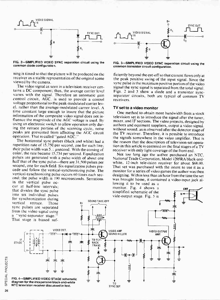
0
VIDEO SIGNAL (P1jjrill.N
C SYNC OUT
RL
FIG. 2-SIMPLIFIED VIDEO SYNC separation circuit using the common diode configuration.
ping is timed so that the picture will be produced on the receiver as a stable representation of the original scene viewed by the camera.
The video signal as seen in a television receiver con- tains a DC component; thus, the average carrier level varies with the signal. Therefore an automatic gain control circuit, AGC, is used to provide a control voltage proportional to the peak -modulated camer lev- el, rather than the average -modulated carrier level. A time constant large enough to insure that the picture information of the composite video signal does not in- fluence the magnitude of the AGC voltage is used. By using an electronic switch to allow operation only dur- ing the retrace portion of the scanning cycle, noise peaks are prevented from affecting the AGC circuit operation. That is called "gated AGC."
The horizontal sync pulses (black and white) had a repetition rate of 15,750 per second, one for each line; their pulse width was 5.1 µsecond. With the coming of color, the rate became 15,734 per second. Equalization pulses are generated wiith a pulse -width of about one half that of the sync pulse-there are 31,500 pulses per second, one for each field. Six equalization pulses pre- cede and follow the vertical -synchronizing pulse. The vertical -synchronizing pulse occurs 60 times each sec- ond; the pulse width is 190 microseconds. Serrations in the vertical pulse oc- cur at half-line intervals; that divides the sync pulse into six individual pulses for synchronization during vertical retrace. Those sync pulses are separated from the video signal using a "sync -separator stage." That stage is biased suf-
IF STAGE
L__
VIDEO DET.
.. . .,.
T
FIG. 4-SIMPLIFIED VIDEO STAGE schematic diagram for the inexpensive black -and -white NTC television receiver disc.issed in text.
g+ SOUND TAKE-OFF
B+
VIDEO SIGNAL "ILA N - -E o
SYNC OUT
o I( C
FIG. 3-SIMPLIFIED VIDEO SYNC separation common transistor circuit configuration.
circuit using the
ficiently beyond the cut-off so that current flows only at the peak positive swing of the input signal. Since the sync pulse is the maximum positive portion of the video signal the sync signal is separated from the total signal. Figs. 2 and 3 show a diode and a transistor sync - separator circuits, both are typical of common TV receivers.
TV set to a video monitor One method to obtain more bandwidth from a stock
television set is to introduce the signal after the tuner, mixer, and IF sections. The video projects, designed by authors and equiment suppliers, output a video signal. without sound, as is observed after the detector stage of the TV receiver. Therefore, it is possible to introduce the signals somewhere in the video amplifier. That is the reason that the description of television -set opera- tion in this article is centered on the final stages of a TV receiver with only light coverage of the front end.
Not too long ago the author purchased an NTC, National Trade Corporation, Model 12O5RA black -and - white, 12 -inch television receiver for about $68.00. That set was purchased with the intent to use it as a monitor for a series of video games the author was then designing. Within less than an hour from the time the set was brought home, it contained a video -input jack al- lowing it to be used as a monitor. Fig. 4 shows a CRT
simplified schematic of the vide -output stage. Fig. 5 is
VIDEO AMP SOUND KILLER
TO SYNC SEP
26
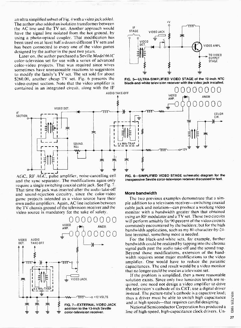
an ultra simplified subset of Fig. 4 with a video jack added. The author also added an isolation transformer between the AC line and the TV set. Another approach would have the signal line isolated from the hot ground, by using a photo -optical coupler. That modification has been used on at least half a dozen different TV sets and has been connected to every one of the video games designed by the author in the past two years.
Later on, the author purchased a Seville Model 661C color -television set for use with a series of advanced color -video projects. That was required since wives sometimes have unreasonable reactions to suggestons to modify the family's TV set. The set sold for about $260.00, another cheap TV set. Fig. 6 presents the video -output section. Note that the video amplifier is
contained in an integrated circuit, along with the IF AUDIO TAKE-OFF
f
IF SECTION
VIDEO DET.
N
SOUND, REJ.
I
aII
7 L -- 4.5 MHz TRAP J
1 1 1
IF STAGE
VIDEO DET.
It
VIDEO JACK
VIDEO AMPL
TO VIDEO OUTPUT STAGE
FIG. 5-ULTRA-SIMPLIFIED VIDEO STAGE of the 12 -inch NTC
black -and -white television receiver with the video jack installed.
00ÓQ
00000000 VIDED
AMP. 0 000AN33100
Y1h ,600
_ __
AGC, RF AGC, pulse amplifier, noise -cancelling cell and the sync separator. The modifications again only require a single switching coaxial cable jack. See Fig. 7. That time the jack was inserted after the audio take-off and sound -rejection circuitry, since the color -video game projects intended as a video source have their own audio amplifiers. Again, AC line isolation between the TV chassis ground of the television receiver and the video source is mandatory for the sake of safety.
VIDEO AUDIO DET. TAKE-OFF
00000000 VIDEO AN331 AMP.
00000
FIG. 7-EXTERNAL VIDEO JACK addition to the 13 -inch Seville color -television receiver.
i
o+12V
COLOR CIR. IR' f '
FIG. 6-SIMPLIFIED VIDEO STAGE schematic diagram for the inexpensive Seville color -television receiver discussed in text.
More bandwidth The two previous examples demonstrate that a sim-
ple addition to a television receiver-switching coaxial cable jack and isolation-can produce a working video monitor with a bandwidth greater than that obtained using an RF modulator and a TV set. Those two circuits will perform amiably for 90 percent of the video circuits commonly encountered by the builders; but for the high bandwidth application, such as my 80 -character -by -24 - line terminal, something more is needed.
For the black -and -white sets, for example, further bandwidth could be realized by tapping into the chroma signal path past the audio take-off and the sound trap. Beyond those modifications, extension of the band- width requires some major modifications to the video amplifier. One would have to reduce the parasitic capacitances. The end result would be a video monitor that no longer could be used as a television set.
If the problem is simplified, then a more reasonable solution exists. Since only two luminous levels are re- quired, one need not design a video amplifier to drive the television's cathode of its CRT; use a digital driver instead. The picture -tube's cathode is a capactive load; thus a driver must be able to switch high capacitance and at high speeds-that requires careful designing.
National Semiconductor Corporation has produced a line of high-speed, high -capacitance clock drivers. Un-
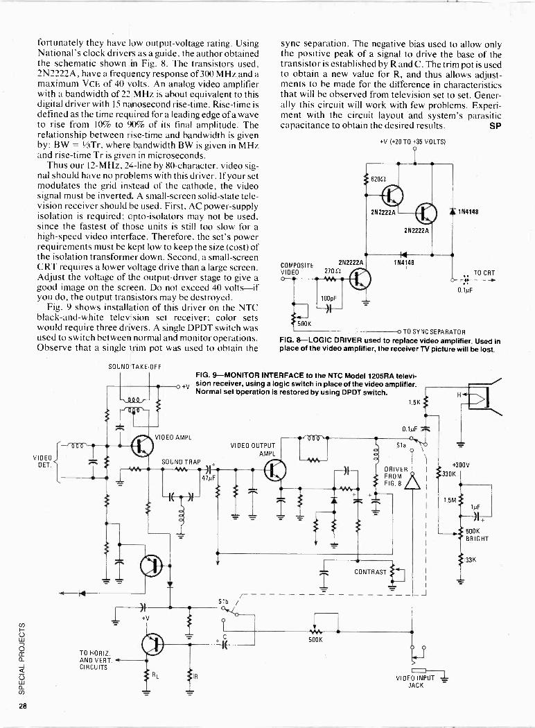
L I
fortunately they have low output -voltage rating. Using National's clock drivers as a guide, the author obtained the schematic shown in Fig. 8. The transistors used, 2N2222A; have a frequency response of 300 MHz and a maximum VCE of 40 volts. An analog video amplifier with a bandwidth of 22 MHz is about equivalent to this digital driver with 15 nanosecond rise -time. Rise -time is defined as the time required for a leading edge of a wave to rise from 10% to 90% of its final amplitude. The relationship between rise -time and bandwidth is given by: BW = 1V3Tr, where bandwidth BW is given in MHz and rise -time Tr is given in microseconds.
Thus our 12 -MHz, 24 -line by 80 -character, video sig- nal should have no problems with this driver. If your set modulates the grid instead of the cathode, the video signal must be inverted_ A small -screen solid-state tele- vision receiver should be used. First, AC power -supply isolation is required; opto -isolators may not be used, since the fastest of those units is still too slow for a high-speed video interface. Therefore, the set's power requirements must be kept low to keep the size (cost) of the isolation transformer down. Second, a small -screen CRT requires a lower voltage drive than a large screen. Adjust the voltage of the output -driver stage to give a good image on the screen. Do not exceed 40 volts-if you do, the output transistors may be destroyed.
Fig. 9 shows installation of this driver on the NTC black -and -white television set receiver; color sets would require three drivers. A single DPDT switch was used to switch between normal and monitor operations. Observe that a single trim pot was used to obtain the
VIDEO D ET.
SOUND -TAKE OFF
TO HORIZ. AND VERT. CIRCUITS
VIDEO AMPL
sync separation. The negative bias used to allow only the positive peak of a signal to drive the base of the transistor is established by R and C. The trim pot is used to obtain a new value for R, and thus allows adjust- ments to be made for the difference in characteristics that will be observed from television set to set. Gener- ally this circuit will work with few problems. Experi- ment with the circuit layout and system's parasitic capacitance to obtain the desired results. SP
+V (+20 TO +35 VOLTS)
2N2222A
252222A
COMPOSITE 2N2222A 154148
VIDEO 27052
100pF
500K o TO SYNC SEPARATOR
FIG. 8-LOGIC DRIVER used to replace video amplifier. Used in place of the video amplifier, the receiver TV picture will be lost.
1N4148
TO CRT
0.1µF
FIG. 9-MONITOR INTERFACE to the NTC Model 1205RA televi- sion receiver, using a logic switch in place of the video amplifier. Normal set operation is restored by using DPDT switch.
SOUND TRAP
47µfF
Sib
+IC(
VIDEO OUTPUT AMPL
500K
1.5K
0.1µF
DRIVER FROM FIG. 8
CONTRAST
I
+300V
330K
1.5M
J
VIDEO INPUT JACK
1µF
+
500 K
BRIGHT
33K

JUNK BOX
METAL
DETECTOR Couple an one -transistor oscillator with a
pocket transistor radio for a sensitive metal detector you can
build this evening.
HERB FRIEDMAN
IT WON'T FIND THE LOST TREASURE OF BLACKBEARD,
the Pirate, or a new mother lode of gold and silver, but the Junk -Box Metal Detector will locate the main water or gas shut-off valve that's buried under a few inches of snow or grass. It will also locate a tuna -salad - on -white sandwich wrapped in tinfoil that was lost at the beach during last summer's company picnic; and it
will keep the junior members of the family busy for hours seeking "Grandpa's Lost Treasure"-a few larger coins buried just under the sand or soil.
It will even locate electrical boxes that someone buried inside a wall; it might detect concealed water pipes and electrical BX cables and conduits if they're near the outer surface of a plaster or drywall; and it will find metallic drain lines concealed behind plaster before you drill into them.
Best of all, you can whip this metal detector together in just a few hours because the critical part-the "de- tector"-is an ordinary transistor pocket radio.
How it works Metal is detected by the sensing transmitter (called
the metal detector) shown in the photographs and schematic diagram; it is indicated by a heterodyne beat in a pocket transistor radio. The Junk Box Metal De- tector unit is a broadcast -band oscillator with an RF output between approximately 1000 and 1600 kHz whose tuning coil, L1, is mounted on the end of a handle. Tuning coil L1's inductive effect is varied when the coil passes over, or is brought in the vicinity of, a metal object. That variation in inductance changes the oscillator's frequency. The exact why of L1's inductance change can be either to ferrus metals
29
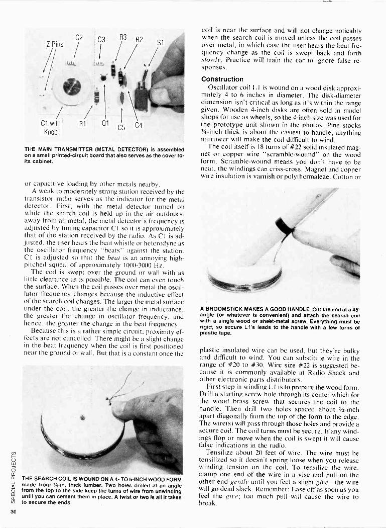
I
C2 e3 R3 R2
Z Pins
1
Cl with
Knob
R1 C11 C5 C4
S1
THE MAIN TRANSMITTER (METAL DETECTOR) is assembled on a small printed -circuit board that also series as the cover for its cabinet.
or capacitive loading by other metals nearby. A weak to moderately strong station received by the
transistor radio serves as the indicator for the metal detector. First, with the metal detector turned on while the search coil its held up in the air outdoors, away from all metal, the metal detector's frequency is adjusted by tuning capacitor Cl so it is approximately that of the station received by the radio. As C 1 is ad- justed, the user hears the beat whistle or heterodyne as the oscillator frequency "beats" against the station. C 1 is adjusted so that the beat is an annoying high- pitched squeal of approximately 1000-3000 Hz.
The coil is swept over the ground or wall with as little clearance as is possible. The coil can even touch the surface. When the coil passes over metal the oscil- lator frequency changes because the inductive effect of the search coil changes. The larger the metal surface under the coil, the greater the change in inductance, the greater the change in oscillator frequency, and hence, the greater the change in the beat frequency.
Because this is a rather simple circuit, proximity ef- fects are not cancelled, There might be a slight change in the beat frequency when the coil is first positioned near the ground or wall. But that is a constant once the
THE SEARCH COIL IS WOUND ON A 4- TO 6 -INCH WOOD FORM made from 3/4 -in. thick lumber. Two holes drilled at an angle from the top to the side keep the turns of wire from unwinding until you can cement them in place. A twist or two is all it takes to secure the ends.
coil is near the surface and will not change noticably when the search coil is moved unless the coil passes over metal, in which case the user hears the beat fre- quency change as the coil is swept back and forth slowly. Practice will train the ear to ignore false re- sponses.
Construction Oscillator coil L1 is wound on a wood disk approxi-
mately 4 to 6 inches in diameter. The disk -diameter dimension isn't critical as long as it's within the range given. Wooden 4 -inch disks are often sold in model shops for use as wheels, so the 4 -inch size was used for the prototype unit shown in the photos. Pine stocks 3/4 -inch thick is about the easiest to handle; anything narrower will make the coil difficult to wind.
The coil itself is 18 turns of #22 solid insulated mag- net or copper wire "scramble -wound" on the wood form. Scramble -wound means you don't have to be neat, the windings can criss-cross. Magnet and copper wire insulation is varnish or polythermaleze. Cotton or
A BROOMSTICK MAKES A GOOD HANDLE. Cut the end at a 45 angle (or whatever is convenient) and attach the search coil with a single wood or sheet -metal screw. Everything must be rigid, so secure L1's leads to the handle with a few turns of plastic tape.
plastic insulated wire can be used, but they're bulky and difficult to wind. You can substitute wire in the range of #20 to #30. Wire size #22 is suggested be- cause it is commonly available at Radio Shack and other electronic parts distributors.
First step in winding L 1 is to prepare the wood form. Drill a starting screw hole through its center which for the wood brass screw that secures the coil to the handle. Then drill two holes spaced about 1/2 -inch apart diagonally from the top of the form to the edge. The wire(s) will pass through those holes and provide a secure coil. The coil turns must be secure. If any wind- ings flop or move when the coil is swept it will cause false indications in the radio.
Tensilize about 20 feet of wire. The wire must be tensilized so it doesn't spring loose when you release winding tension on the coil. To tensilize the wire, clamp one end of the wire in a vise and pull on the other end gently until you feel a slight give-the wire will go dead slack. Remember: Ease off as soon as you feel the give; too much pull will cause the wire to break.
30
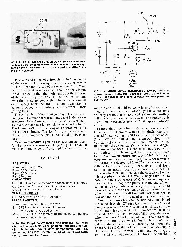
Z PIN
Z pins
NO! THE LETTERING ISN'T UPSIDE DOWN. Your hand will be at
the top, so the entire transmitter is mounted the "wrong way" on the handle. The wires from L1 are wrapped around the Z pins and then soldered.
Pass one end of the wire through a hole from the side of the wood disk, allowing about 3 inches of wire to stick out through the top of the wood -coil form. Wind 18 turns as tight as is possible, then push the winding so you can get at the other hole, and pass the free end of the wire through the hole. Pull both wires tight and twist them together two or three times so the winding can't spring back. Saturate the coil with airplane cement, Duco, or a similar glue to prevent it from getting loose.
The remainder of the circuit (see Fig. 1) is assembled on a printed -circuit board (see Figs. 2 and 3) that serves as a cover for a plastic case approximately 21/2 x 1% x 4 inches. A full-scale foil templet is provided in Fig. 2.
The layout isn't critical as long as it approximates the foil pattern shown. The foil "square" serves as a shield for tuning -capacitor C 1 and should not be elimi- nated.
You can substitute a general replacement transistor for the specified transistor, Q1 (see Fig. 1). To avoid excessive frequency shifts caused by heat from the
PARTS LIST
RESISTORS 1/4 watt or 1/2 watt, 10% R1-47,000 ohms R2-10,000 ohms R3-270 ohms CAPACITORS C1-365-pF miniature polyvaricon capacitor with dial knob C2, C3-100-pF tubular ceramic or mica, see text C4, C5 -0.05-µF ceramic disc or Mylar SEMICONDUCTOR Q1-NPN transistor, 2N2484 or equiv. MISCELLANEOUS L1-Homebrew search coil, see text S1-SPST printed circuit switch, see text B1-9 volt battery, type 2U6 or equiv. Misc.-Cabinet, #22 enamel wire, battery holder, handle.
hook-up wire, solder, etc.
Note. The 365-pF polyvaricon tuning capacitor, (C1) with dial knob is available for $6 postpaid (postage and han- dling included) from Custom Components, Box 153,
Malverne, NY 11565. NY State residents must add sales tax. $1 additional to Canada.
S1
C5
.05
B1
9V
I
C4 R2
1.05 10K
-H H1/8" TOP
3/16" SIDE
FOIL SIDE 1/4
PIN
FIG. 1-JUNKBOX METAL DETECTOR SCHEMATIC DIAGRAM
shows a simple RF oscillator. Loading on coil L1 determines the
amount of detuning, or drifting of frequency. from preset fre- quency by Cl.
ZIP CABLE
C2
100pF
C3
100pF
Z PIN
L1
E B C
000
01 2N2484 BOTTOM VIEW
sun, C2 and C3 should be some form of mica, silver mica, or tubular ceramic; but if all you have are some ordinary ceramic discs go ahead and use them-they will probably work reasonably well. (The author's unit uses tubular ceramics from a "100 -capacitors -for -$2
kit".) Printed -circuit switches don't usually come cheap.
However, a flat mount with PC terminals, was pur- chased for something like $1 from Chaney Electronics. (It's convenient to install and á great buy! Stock up if
you can.) If you substitute a different switch, change the printed -circuit template's connections accordingly.
Tuning -capacitor C 1 is a 365-pF miniature polyvari- con with a 11/4 inch tuning dial that also serves as a
knob. You can substitute any type of 365-pF "poly" capacitor because all common poly capacitor terminals will fit the PC foil layout. Make C l's connections care- fully. C l's lugs are usually "brite-finish" and don't take, solder easily; but you cannot use excessive soldering heat or you'll damage the capacitor. Follow this procedure to install Cl: Wrap a single turn of solid hook-up wire around each of C l's lugs and squeeze them tight with long nose pliers. Dip the end of your solder in non -corrosive (non acid) soldering paste and then solder a wire to the lug. Then do it again for the other solder joint. It will take little soldering heat if
you use the paste. But remember, just a dab will do. Coil L l's connections to the printed -circuit board
are made through "Z" pins fashioned from #20 solid wire, or you can use a wire wrap terminal (such as sold by Chaney Electronics). The connections must be formed into a "Z" so they don't fall through the board when the wires from L I are soldered. The dimensions for the "Z" pins are shown in Fig. 1. They aren't criti- cal; any shape that keeps them from falling through the board will be OK. While L1 can be soldered directly to the board, the "Z" terminals will allow you to easily remove L I without damage to the foils if the checkout
2 INCHES
FIG. 2-USE THE AUTHOR'S PC TEMPLATE for best results. Make exact same -size copy including the large square area that serves as a shield for capacitor Cl.
shows L 1 wasn't properly wound and you have to dis- connect it from the PC board.
Battery B1, a 9 -volt type such as used for transistor radios, is held inside the plastic cabinet by a small transistor battery clamp sold by Radio Shack (among others).
The handle is about 3 -feet long...use whatever length is convenient for you. Either cut down an old broom handle or buy a 1 or 11/2 -inch diameter wood dowel. Cut the bottom end at a 45 -degree angle. Secure the plastic cabinet to the handle about %a down from the top. Then secure coil L1 to the bottom with a single screw passing through the center of the form. Scrape the insulation from the free ends of LI, tin with solder, and attach a length of plastic insulated zip wire such as you would use to connect speakers to an amplifier. (The extra -thin stuff, #22 or #24, is sug- gested.) Insulate the connections with shrink tubing or spaghetti and secure the zip wire to the handle with a turn or two or plastic tape. Run the wire up the handle and connect to the two "Z" terminals on the PC board.
Test before using Tune a pocket radio to a station at about 1000 kHz.
Turn on the metal detector and slowly adjust C 1. At some point you should hear the heterodyne whistle in the radio. If you don't hear the whistle, tune to a station higher in frequency, say 1100 kHz, and try again. If you cannot hear a whistle all the way up to 1600 kHz check for wiring error. If you can get the heterodyne beats only on stations near the top of the dial, above 1300 kHz, most likely there is something wrong with LI; it probably needs a few turns of wire, or the form
Cl SHAFT CENTER
Z PINS TO L1
9V FIG. 3-PARTS LAYOUT FOR THE PRINTED -CIRCUIT BOARD. You may have to modify the board a bit to compensate for dif- ferent battery switch Si if you do not use author's manufac- tured type. Leads connected to C1's terminals connect to terminals on PC board. See text for details.
is less than 4 inches in diameter. But if you can receive a top -of -the -band station clearly, and you get a clean heterodyne, you can still use the detector.
Using the metal detector If you place the radio too close to the metal detector
if will be jammed by the metal detector, so don't secure it to the handle. The shirt pocket is a good loca- tion. On the other hand, if the received signal is too strong it will jam out the signal from the metal detector.
Try to use a station of weak -to-moderate signal strength. Turn on the metal detector, hold the coil in the air, and adjust C 1 for a high pitched, raucous squeal from the radio. Then sweep the search coil.
If C 1 is set so that the heterodyne beat is a low fre- quency, you will hardly notice minute changes in tone quality produced by small quantities of metal under the search coil. Shoot for an adjustment of CI that pro- vides a tone in the range of 1000 to 3000 Hz-fre- quencies to which the ear is most sensitive.
You must remember that the Metal Detector oscil- lator circuit produces signals on the broadcast band. Do not let the unit run when not necessary for fear of interfering with another's listening pleasure. SP
Now! Learn on the latest...
NRI traininçj includes 25" Heath/Zenith color TV with state-of-the-art features;;
6 -function infrared remote control space phone lets you answer or call from your chair microprocessor -controlled PLL varactor tuner 82 VHF/UHF, 35 cable channels 24 -hour programmable channel selection electronic time display 4 -speaker FM sound system choice of three cabinets at student discount
We've taken the finest, most advanced, most
complete TV/Audio/Video course available and
made it even better. Now NRI brings your training up to and even beyond today's technology with the
exciting, advanced performance Heath/Zenith
Model 2501 TV. Now you can learn how to service
even the latest circuitry on the most expensive TV
sets as you assemble and perform experiments on
your Heathkit/Zenith. Only NRI combines such
complete training with such up-to-date equipment.
Choice of Three Specialties And only NRI gives you the opportunity to
specialize in any of three areas. You get the same
complete training covering TV, audio systems, and
video recorders, but you select your own specialty
for practical, hands-on training. You can choose to build the Heath/Zenith
color TV; specialize in audio systems and build
your own AM/FM stereo system; or take your bench
Choice of specialty training on 11, stereo, or VCR
training with remote -controlled videocassette re-
corder featuring NRI training on videotape. No
matter which specialty you elect, your practical
training also includes experiments and demonstra-
tions with the exclusive NRI Discovery Lab® and your own professional digital multimeter. All
equipment is yours to use and keep.
Learn in Your Spare Time No need to quit your job or tie up your
evenings with night school...no classroom com-
petition or rigid schedules. NRI trains you in your
own home at your convenience. You're a class
of one with complete course materials, practical
training on the latest equipment, and the backing
of a full staff of professional electronics educators.
NRI brings it all to you.
The Professional's Choice A million and a half students have already
chosen the NRI way. And over half the practicing
TV service technicians in the U.S. have advanced
their careers with convenient home training.
Among them, it's NRI 3 to 1 over any other school
(summary of national survey on request).
Free Catalog... No Salesman Will Call
Get all the facts on complete, convenient
NRI training. See all the equipment, look over
complete lesson plans, check out our convenient
time payment plans. And see the many other
opportunities in fields like Microcomputers, Elec-
tronic Design, Communications Electronics, and
more. Send postage -paid card and see what ad-
vanced training is all about. If card has been
removed, please write to us.
Practical training on a real state -óf -the -art TV using professional ei uilpnent
NRI rfe
iñIY We'll give you tomorrow.
NRI Schools McGraw-Hill Continuing
Education Center
3939 Wisconsin Ave.
Washington, D.C. 20016
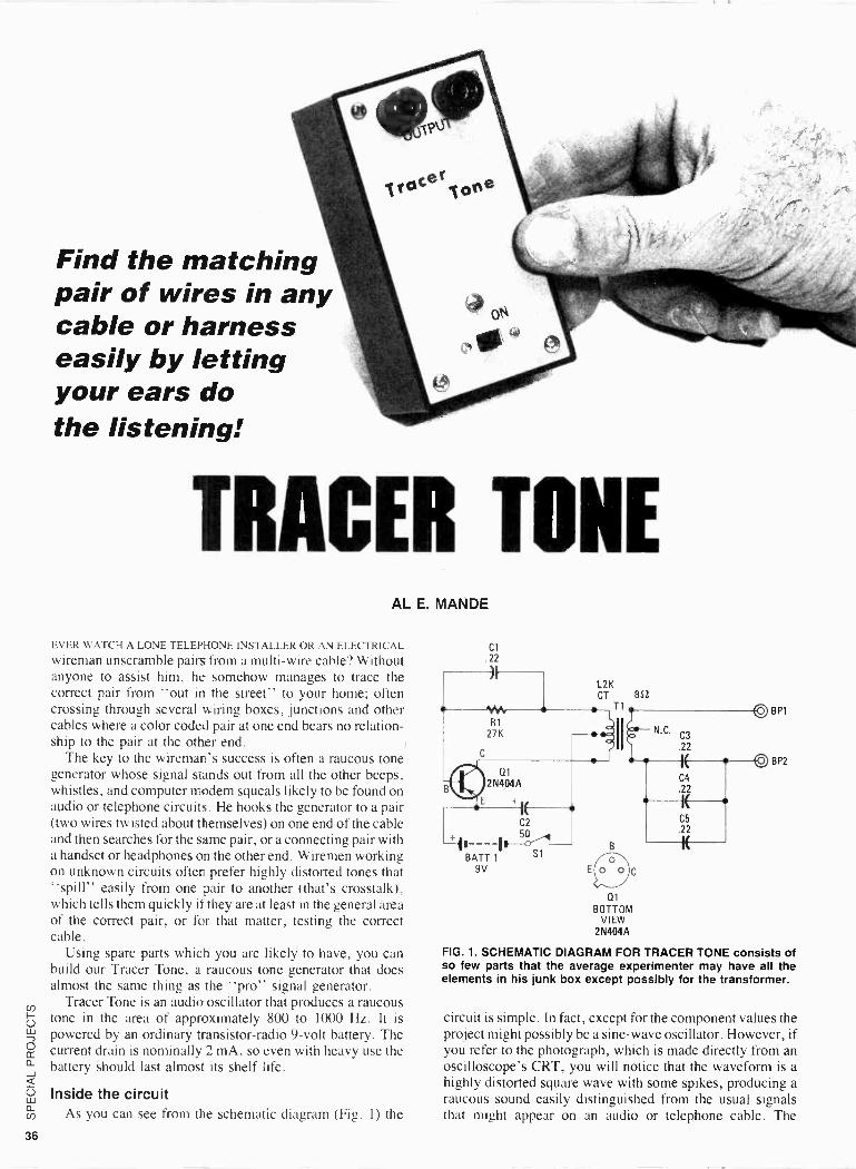
Find the matching pair of wires in any cable or harness easily by letting your ears do the listening!
TRACER TONE AL E. MANDE
EVER WATCH A LONE TELEPHONE INSTALLER OR AN ELECTRICAL
wireman unscramble pairs from a multi -wire cable? Without anyone to assist him, he somehow manages to trace the correct pair from "out in the street" to your home; often crossing through several wiring boxes, junctions and other cables where a color coded pair at one end bears no relation- ship to the pair at the other end.
The key to the wireman's success is often a raucous tone generator whose signal stands out from all the other beeps, whistles, and computer modem squeals likely to be found on audio or telephone circuits. He hooks the generator to a pair (two wires twisted about themselves) on one end of the cable and then searches for the same pair, or a connecting pair with a handset or headphones on the other end. Wiremen working on unknown circuits often prefer highly distorted tones that "spill" easily from one pair to another (that's crosstalk), which tells them quickly if they are at least in the general area of the correct pair, or for that matter, testing the correct cable.
Using spare parts which you are likely to have, you can build our Tracer Tone, a raucous tone generator that does almost the same thing as the "pro" signal generator.
Tracer Tone is an audio oscillator that produces a raucous tone in the area of approximately 800 to 1000 Hz. It is powered by an ordinary transistor -radio 9 -volt battery. The current drain is nominally 2 mA, so even with heavy use the battery should last almost its shelf life.
Inside the circuit As you can see from the schematic diagram (Fig. 1) the
Cl .22
Q1
2N404A
C2
50 --- F O-- BATT 1
Si
9V
1.2K CT 82
Ti
O1
BOTTOM VIEW
2N404A
BP1
BP2
FIG. 1. SCHEMATIC DIAGRAM FOR TRACER TONE consists of so few parts that the average experimenter may have all the elements in his junk box except possibly for the transformer.
circuit is simple. In fact, except for the component values the project might possibly be a sine -wave oscillator. However, if you refer to the photograph, which is made directly from an oscilloscope's CRT, you will notice that the waveform is a highly distorted square wave with some spikes, producing a raucous sound easily distinguished from the usual signals that might appear on an audio or telephone cable. The
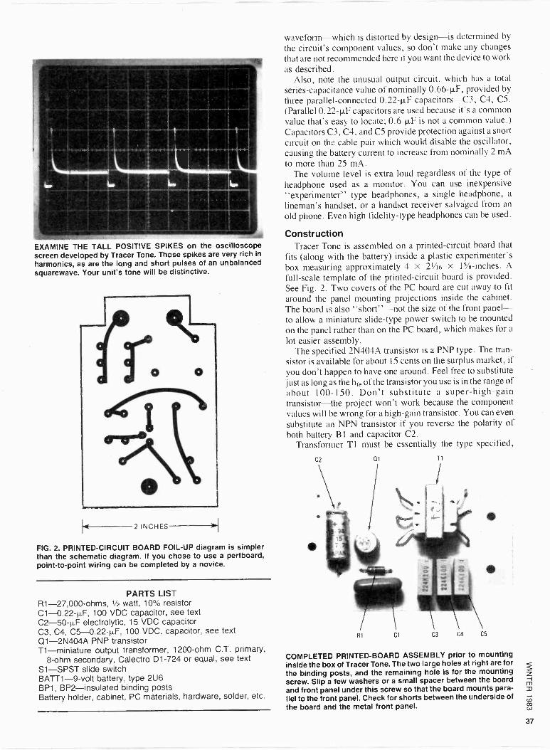
EXAMINE THE TALL POSITIVE SPIKES on the oscilloscope screen developed by Tracer Tone. Those spikes are very rich in
harmonics, as are the long and short pulses of an unbalanced squarewave. Your unit's tone will be distinctive.
(3-00 o
2 INCHES
FIG. 2. PRINTED -CIRCUIT BOARD FOIL -UP diagram is simpler than the schematic diagram. If you chose to use a perfboard, point-to-point wiring can be completed by a novice.
PARTS LIST R1 -27,000 -ohms, '/z watt, 10% resistor C1 -0.22-µF, 100 VDC capacitor, see text C2 -50-µF electrolytic, 15 VDC capacitor C3, C4, C5 -0.22-µF, 100 VDC, capacitor, see text Q1 -2N404Á ,PNP transistor T1-miniature output transformer, 1200 -ohm C.T. primary,
8 -ohm secondary, Calectro D1-724 or equal, see text S1-SPST slide switch BATT1-9-volt battery, type 2U6 BP1, BP2-insulated binding posts Battery holder, cabinet, PC materials, hardware, solder, etc.
waveform-which is distorted by design-is determined by
the circuit's component values, so don't make any changes that are not recommended here if you want the device to work as described.
Also, note the unusual output circuit, which has a total series -capacitance value of nominally 0.66-µF, provided by
three parallel -connected 0.22-µF capacitors-C3, C4, C5. (Parallel 0.22-µF capacitors are used because it's a common value that's easy to locate; 0.6-µF is not a common value.) Capacitors C3, C4, and C5 provide protection against a short circuit on the cable pair which would disable the oscillator, causing the battery current to increase from nominally 2 mA
to more than 25 mA. The volume level is extra loud regardless of the type of
headphone used as a monitor. You can use inexpensive "experimenter" type headphones, a single headphone, a
lineman's handset, or a handset receiver salvàged from an
old phone. Even high fidelity -type headphones can be used.
Construction Tracer Tone is assembled on a printed -circuit board that
fits (along with the battery) inside a plastic experimenter's box measuring approximately 4 x 21h6 x 15/8 -inches. A
full-scale template of the printed -circuit board is provided. See Fig. 2. Two covers of the PC board are cut away to fit
around the panel mounting projections inside the cabinet. The board is also "short"-not the size of the front panel- to allow a miniature slide -type power switch to be mounted on the panel rather than on the PC board, which makes for a
lot easier assembly. The specified 2N404A transistor is a PNP type. The tran-
sistor is available for about 15 cents on the surplus market, if you don't happen to have one around. Feel free to substitute just as long as the hfe of the transistor you use is in the range of about 100-150. Don't substitute a super -high -gain transistor-the project won't work because the component values will be wrong for a high -gain transistor. You can even substitute an NPN transistor if you reverse the polarity of both battery B 1 and capacitor C2.
Transformer T1 must be essentially the type specified,
C2
R1
at
C1
TI
C3 C4 C5
COMPLETED PRINTED -BOARD ASSEMBLY prior to mounting inside the box of Tracer Tone. The two large holes at right are for the binding posts, and the remaining hole is for the mounting screw. Slip a few washers or a small spacer between the board and front panel under this screw so that the board mounts para- llel to the front panel. Check for shorts between the underside of the board and the metal front panel.
37
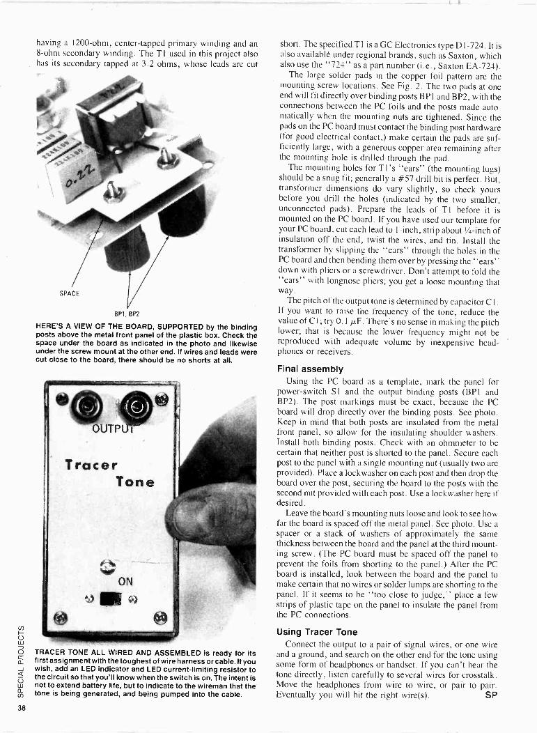
L 1
having a 1200 -ohm, center -tapped primary winding and an 8 -ohm secondary winding. The T1 used in this project also has its secondary tapped at 3.2 ohms, whose leads are cut
BP1, BP2
HERE'S A VIEW OF THE BOARD, SUPPORTED by the binding posts above the metal front panel of the plastic box. Check the space under the board as indicated in the photo and likewise under the screw mount at the other end. If wires and leads were cut close to the board, there should be no shorts at all.
TRACER TONE ALL WIRED AND ASSEMBLED is ready for its first assignment with the toughest of wire harness or cable. If you wish, add an LED indicator and LED current -limiting resistor to the circuit so that you'll know when the switch is on. The intent is not to extend battery life, but to indicate to the wireman that the tone is being generated, and being pumped into the cable.
short. The specified T1 is a GC Electronics type D1-724. It is also available under regional brands, such as Saxton, which also use the "724" as a part number (i.e., Saxton EA -724).
The large solder pads in the copper foil pattern are the mounting screw locations. See Fig. 2. The two pads at one end will fit directly over binding posts BP 1 and BP2, with the connections between the PC foils and the posts made auto- matically when the mounting nuts are tightened. Since the pads on the PC board must contact the binding post hardware (for good electrical contact,) make certain the pads are suf- ficiently large, with a generous copper area remaining after the mounting hole is drilled through the pad.
The mounting holes for T1 's "ears" (the mounting lugs) should be a snug fit; generally a #57 drill bit is perfect. But, transformer dimensions do vary slightly, so check yours before you drill the holes (indicated by the two smaller, unconnected pads). Prepare the leads of T1 before it is mounted on the PC board. If you have used our template for your PC board, cut each lead to 1 -inch, strip about''/ -inch of insulation off the end, twist the wires, and tin. Install the transformer by slipping the "ears" through the holes in the PC board and then bending them over by pressing the "ears" down with pliers or a screwdriver. Don't attempt to fold the "ears" with longnose pliers; you get a loose mounting that way.
The pitch of the output tone is determined by capacitor C l .
If you want to raise the frequency of the tone, reduce the value of Cl; try 0.1 µF. There's no sense in making the pitch lower; that is because the lower frequency might not be reproduced with adequate volume by inexpensive head- phones or receivers.
Final assembly Using the PC board as a template, mark the panel for
power -switch Si and the output binding posts (BP1 and BP2). The post markings must be exact, because the PC board will drop directly over the binding posts. See photo. Keep in mind that both posts are insulated from the metal front panel, so allow for the insulating shoulder washers. Install both binding posts. Check with an ohmmeter to be certain that neither post is shorted to the panel. Secure each post to the panel with a single mounting nut (usually two are provided). Place a lockwasher on each post and then drop the board over the post, securing the board to the posts with the second nut provided with each post. Use a lockwasher here if desired.
Leave the board's mounting nuts loose and look to see how far the board is spaced off the metal panel. See photo. Use a spacer or a stack of washers of approximately the same thickness between the board and the panel at the third mount- ing screw. (The PC board must be spaced off the panel to prevent the foils from shorting to the panel.) After the PC board is installed, look between the board and the panel to make certain that no wires or solder lumps are shorting to the panel. If it seems to be "too close to judge," place a few strips of plastic tape on the panel to insulate the panel from the PC connections.
Using Tracer Tone Connect the output to a pair of signal wires, or one wire
and a ground, and search on the other end for the tone using some form of headphones or handset. If you can't hear the tone directly, listen carefully to several wires for crosstalk. Move the headphones from wire to wire, or pair to pair. Eventually you will hit the right wire(s). SP
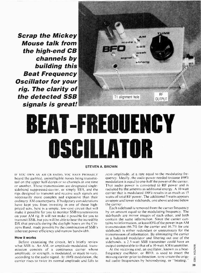
Scrap the Mickey Mouse talk from the high -end CB
channels by building this
Beat Frequency Oscillator for your rig. The clarity of the detected SSB
signals is great!
BEAT -FREQUENCY
OSCILLATOR STEVEN A. BROWN
IF YOU OWN AN AM CB RADIO, YOU HAVE PROBABLY heard the garbled, unintelligible noises being transmit- ted on the upper half -dozen or so channels at one time or another. Those transmissions are designated single- sideband suppressed -carrier, or simply SSB, and the rigs designed to transmit and receive such signals are necessarily more complex and expensive than their ordinary AM counterparts. If budgetary considerations have kept you from investing in one of those high- priced sets, here is a simple. low-cost circuit that will make it possible for you to monitor SSB transmissions on your AM rig. It will not make it possible for you to transmit SSB, but you will be able to hear the incredible DX that prevails during the daylight hours on the Citi- zens Band, made possible by the combination of SSB's inherent power efficiency and narrow bandwidth.
How it works Before examining the circuit, let's briefly review
what SSB is. An AM, or amplitude -modulated, trans- mission consists of a continuous camer whose amplitude, or strength, is modulated, or made to vary, according to the audio signal. At 100% modulation, the carrier rises to twice its normal amplitude and falls to
zero amplitude, at a rate equal to the modulating fre- quency. Ideally, the audio power needed to cause 100% modulation is equal to one-half the power of the carrier. That audio power is converted to RF power and is radiated by the antenna as additional energy. A 10 -watt carrier that is modulated 100% results in as much as 15
watts of total RF power. The additional 5 watts appears as upper and lower sidebands, one above and one below the carrier.
Each sideband is removed from the carrier frequency by an amount equal to the modulating frequency. The sidebands are mirror images of each other, and both contain the same information. Since the carrier con- tains no information, at least 83% of the power in an AM transmission (66.7% for the camer and 16.7% for one sideband) is either redundant or unnecessary for the transmission of information. By eliminating the carrier in a balanced modulator and filtering out one of the sidebands, a 2.5 -watt SSB transmitter could have an output comparable to that of a 10 -watt AM transmitter.
At the receiving end, an oscillator, known as a beat - frequency oscillator, or BFO, is used to insert the missing carrier prior to detection, to re-create the origi- nal audio frequencies by heterodyning, or "beating,"
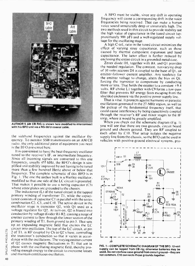
AUTHOR'S AM CB RIG is shown here modified to interconnect with his BFO unit via a RG -58/U coaxial cable.
the sideband frequencies against the oscillator fre- quency. To monitor SSB transmissions on an AM CB radio, the only additional piece of equipment you need is the BFO presented here.
It is convenient to have the beat -frequency oscillator tuned to the receiver's IF, or intermediate frequency. Since all incoming signals are converted to this one frequency, usually 455 kHz, the BFO's design is sim- plified and stability improved by not having to be tuned more than a few hundred Hertz above or below that frequency. The complete schematic of this BFO is in Fig. 1. The one the author built is a Hartley oscillator, modified so that one side of the LC circuit is grounded. That makes it possible to use a tuning capacitor (C3) whose rotor plates are grounded to the chassis.
The inductance (L) of the tuned circuit is the tapped primary winding of transformer T1, while the capaci- tance consists of capacitor C l in parallel with the series combination C2, C3, and C10. The active device in the oscillator stage is transistor Q2, with Q 1 used as a voltage regulator for Q2. At turn -on, Q2 is biased into conduction by voltage divider RI -R2, causing a surge of emitter current to flow through the lower section of the primary winding of TI, from ground to pin 5. That sets up an expanding magnetic field that excites the LC circuit into oscillation. The top of the LC circuit, at pin 2 of T I, is RF coupled by C6 to Q2's base, controlling the transistor's conduction so that it varies in accor- dance with the oscillations. The varying emitter current of Q2 causes magnetic fluctuations in T1 that are in phase with the oscillating magnetic field, thereby pro- viding enough energy to the circuit to overcome losses and maintain continuous oscillation.
A BFO must be stable, since any drift in operating frequency will cause a corresponding drift in the voice frequencies being received. That can make a human voice sound unnaturally deep or unnaturally high. The two methods used in this circuit to provide stability are the high value of capacitance in the tuned circuit (ap- proximately 900 pF) and a well -regulated supply vol- tage for the oscillating stage.
A high C-toL ratio in the tuned circuit minimizes the effect of varying stray capacitance, such as those caused by thermal component expansion and hand capacitance. The latter effect is further reduced by enclosing the entire circuit in a grounded metal case.
Zener diode Dl , together with R4, and Q 1 provides the needed regulation. The constant, nonvarying drop of 10 volts accross Dl is coupled to the base of Q I, an emitter -follower current amplifier. Any tendency for the emitter voltage to change, alters the bias on Ql, forcing the transistor to compensate by conducting more or less. That holds the emitter to a constant +9.4 volts. RF choke L I together with C9 forms a low-pass filter that prevents RF energy from escaping from the shielded enclosure via the positive power supply line.
That is vital. It protects against harmonic or parasitic oscillations generated in the 27 -MHz region, as well as the pickup of the fundamental frequency itself, that could cause interference by being capacitively coupled through the receiver's RF and mixer stages to the IF strip, where it would be greatly amplified.
When you check out the schematic diagram (Fig. I) you will see that there are two grounds, circuit board ground and chassis ground. They are RF coupled to each other by C10. That setup isolates the negative supply line from the chassis, so the BFO can be used in vehicles with positive -ground electrical systems, pro -
12V
R.F. OUTPUT
r AM o S1
L1
2.5mH
SSB C9
I WEAK
STRONG
.l ca 10pF
C5
18pF
S2
01 10V
R1
47K
C6
001
C2
100pF
Cl R2
680pF
C10 01
C3
5-
100pF
01 252222
02 ECG.103A
R3
47052
C7I 011
J
FIG. 1-COMPLETE SCHEMATIC DIAGRAM OF THE BFO. 12 -volt supply can be tapped from CB rig; otherwise batteries may be used. Do not confuse case ground from circuit ground-they are not common. C10 connects those grounds together.
40
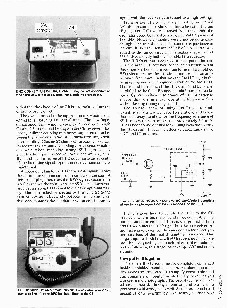
ANT BNC
coonector
\
BNC CONNECTOR ON BACK PANEL may be left unconnected when the BFO is not used. Note that it adds no extra depth.
vided that the chassis of the CB is also isolated from the circuit board ground.
The oscillator coil is the tapped primary winding of a 455 -kHz slug -tuned IF transformer. The low -impe- dance secondary winding couples RF energy through C4 and C5 to the final IF stage in the CB receiver. That loose, indirect coupling minimizes any interaction be- tween the receiver and the BFO, further assuring oscil- lator stability. Closing S2 shunts C4 in parallel with C5, increasing the amount of coupling capacitance. which is desirable when receiving strong SSB signals. The switch is left open to receive normal and weak signals. By matching the degree of BFO coupling to the strength of the incoming signal, optimum receiver sensitivity is
maintained. A loose coupling to the BFO for weak signals allows
the automatic volume control to set maximum gain. A tighter coupling increases the BFO signal, causing the AVC to reduce the gain. A strong SSB signal, however, requires a strong BFO signal to maintain optimum clar- ity. The gain reduction caused by throwing S2 to the STRONG position effectively reduces the volume blast that accompanies the sudden appearance of a strong
ALL HOOKED UP AND READY TO GO! Here's what your CB rig may look like after the BFO has been fitted to the CB.
signal with the receiver gain turned to a high setting. Transformer T1's primary is shunted by an internal
180-pF capacitor, not shown in the schematic diagram (Fig. 1), and if Cl were removed from the circuit, the oscillator could be tuned to a fundamental frequency of 455 kHz. However, stability would not be quite good enough, because of the small amount of capacitance in the circuit. For that reason, 680 pF of capacitance was added to the tuned circuit. This makes it resonant at 227.5 kHz, exactly half the 455 -kHz IF frequency.
The BFO's output is coupled to the input of the final IF stage in the CB receiver. Since the collector load of this stage is a 455 -kHz tuned transformer, the amplified BFO signal excites the LC circuit into oscillation at its resonant frequency. In that way the final IF stage in the receiver serves as a frequency -doubler for the BFO. The second harmonic of the BFO, at 455 kHz, is also amplified by the final IF stage and reinforces the oscilla- tions. C 1 should have a tolerance of 10% or better to ensure that the intended operating frequency falls within the slug -tuning range of T l .
The desirable range of tuning after T1 has been ad- justed, is only a few hundred Hertz above and below that frequency, to allow for the frequency tolerance of SSB transmitters. A range of approximately 2.5 to 50 pF has been found optimal for a tuning capacitor across the LC circuit. That is the effective capacitance range of C2 and C3 in series.
INPUT FROM PREVIOUS IF STAGE
INPUT FROM BFO
IF TRANSFORMER r--- --I
l L _1 J ___
+vcc
AVC
AUDIO
1 T
FIG. 2-SIMPLE HOOK-UP SCHEMATIC DIAGRAM illustrating where to couple signal from the CB second IF to the BFO.
Fig. 2 shows how to couple the BFO to the CB receiver. Use a length of 52 -ohm coaxial cable, the outer conductor connected to chassis ground at both ends, to conduct the BFO signal into the transceiver. At the transceiver, connect the inner conductor directly to the base lead of the final IF amplifier transistor. This stage amplifies both IF and BFO frequencies, which are then heterodyned against each other in the diode de- tector following this stage, to develop AVC and audio signals.
Now put it all together The entire BFO circuit must be completely contained
inside a shielded metal enclosure. An aluminum mini - box makes an ideal case. To simplify construction, all components are mounted inside the top cover, as you can see in the photographs. The prototype uses a print- ed circuit board, although point-to-point wiring on a perf board will work just as well. Since the circuit board measures only 2 -inches by 1.75 -inches, a 1 -inch 6-32
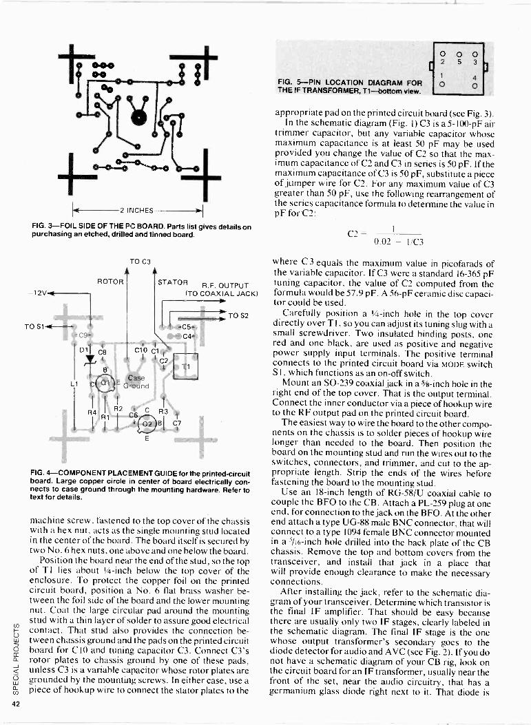
f` 2 INCHES
FIG. 3-FOIL SIDE OF THE PC BOARD. Parts list gives details on purchasing an etched, drilled and tinned board.
-12V L
TO S1
- C9 -
L1
TO C3
ROTOR STATOR R.F. OUTPUT (TO COAXIAL JACK)
C10 Cl
C2.
E
TO S2
-05- -C4-
TI
R3
C7
FIG. 4-COMPONENT PLACIEMENT GUIDE for the printed -circuit board. Large copper circle in center of board electrically con- nects to case ground through the mounting hardware. Refer to text for details.
machine screw, fastened to the top cover of the chassis with a hex nut, acts as the single mounting stud located in the center of the board. The board itself is secured by two No. 6 hex nuts, one above and one below the board.
Position the board near the end of the stud, so the top of TI lies about 1/4 -inch below the top cover of the enclosure. To protect the copper foil on the printed circuit board, position a No. 6 flat brass washer be- tween the foil side of the board and the lower mounting nut. Coat the large circular pad around the mounting stud with a thin layer of solder to assure good electrical contact. That stud also provides the connection be- tween chassis ground and the pads on the printed circuit board for C 10 and tuning capacitor C3. Connect C3's rotor plates to chassis ground by one of these pads, unless C3 is a variable capacitor whose rotor plates are grounded by the mounting screws. In either case, use a piece of hookup wire to connect the stator plates to the
FIG. 5-PIN LOCATION DIAGRAM FOR THE IF TRANSFORMER, T1-bottom view.
c
O O O 2 5 3
1
O 4
O
appropriate pad on the printed circuit board (see Fig. 3). In the schematic diagram (Fig. 1) C3 is a 5-100-pF air
trimmer capacitor, but any variable capacitor whose maximum capacitance is at least 50 pF may be used provided you change the value of C2 so that the max- imum capacitance of C2 and C3 in series is 50 pF. If the maximum capacitance of C3 is 50 pF, substitute a piece of jumper wire for C2. For any maximum value of C3 greater than 50 pF, use the following rearrangement of the series capacitance formula to determine the value in pF for C2:
C2 - 1
0.02 - 1/C3
where C 3 equals the maximum value in picofarads of the variable capacitor. If C3 were a standard 16-365 pF tuning capacitor, the value of C2 computed from the formula would be 57.9 pF. A 56-pF ceramic disc capaci- tor could be used.
Carefully position a 1/4 -inch hole in the top cover directly over T 1, so you can adjust its tuning slug with a small screwdriver. Two insulated binding posts, one red and one black, are used as positive and negative power supply input terminals. The positive terminal connects to the printed circuit board via MODE switch S 1, which functions as an on -off switch.
Mount an SO -239 coaxial jack in a 1/4 -inch hole in the right end of the top cover. That is the output terminal. Connect the inner conductor via a piece of hookup wire to the RF output pad on the printed circuit board.
The easiest way to wire the board to the other compo- nents on the chassis is to solder pieces of hookup wire longer than needed to the board. Then position the board on the mounting stud and run the wires out to the switches, connectors, and trimmer, and cut to the ap- propriate length. Strip the ends of the wires before fastening the board to the mounting stud.
Use an I8 -inch length of RG -58/U coaxial cable to couple the BFO to the CB. Attach a PL -259 plug at one end, for connection to the jack on the BFO. At the other end attach a type UG-88 male BNC connector, that will connect to a type 1094 female BNC connector mounted in a 5/16 -inch hole drilled into the back plate of the CB chassis. Remove the top and bottom covers from the transceiver, and install that jack in a place that will provide enough clearance to make the necessary connections.
After installing the jack, refer to the schematic dia- gram of your transceiver. Determine which transistor is the final IF amplifier. That should be easy because there are usually only two IF stages, clearly labeled in the schematic diagram. The final IF stage is the one whose output transformer's secondary goes to the diode detector for audio and AVC (see Fig. 2). If you do not have a schematic diagram of your CB rig, look on the circuit board for an IF transformer, usually near the front of the set, near the audio circuitry, that has a germanium glass diode right next to it. That diode is
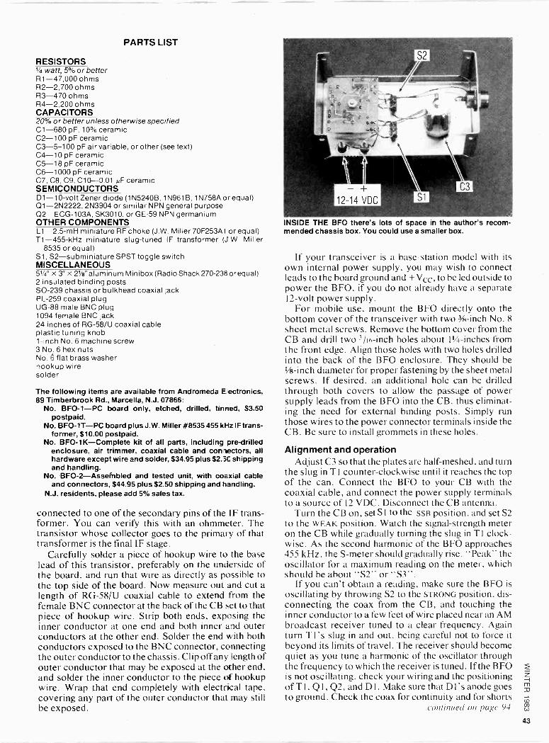
PARTS LIST
RESISTORS 1/4 watt, 5% or better R1-47,000 ohms R2-2,700 ohms R3-470 ohms R4-2,200 ohms CAPACITORS 20% or better unless otherwise specified C1-680 pF, 10% ceramic C2-100 pF ceramic C3-5-100 pF air variable, or other (see text) C4-10 pF ceramic C5-18 pF ceramic C6-1000 pF ceramic C7, C8, C9, C10-0.01 uF ceramic SEMICONDUCTORS D1 -10 -volt Zener diode (1 N5240B, 1 N961 B, 1 N758A or equal) Q1 -2N2222, 2N3904 or similar NPN general purpose Q2-ECG-103A, SK3010, or GE -59 NPN germanium OTHER COMPONENTS L1-2.5-mH miniature RF choke (J.W. Miller 70F253A1 or equal) T1 -455 -kHz miniature slug -tuned IF transformer (J.W. Miller
8535 or equal) S1, S2-subminiature SPST toggle switch MISCELLANEOUS 51/4' x 3" x 21/8" aluminumMinibox(RadioShack270-238orequal) 2 insulated binding posts SO -239 chassis or bulkhead coaxial jack PL -259 coaxial plug UG-88 male BNC plug 1094 female BNC jack 24 inches of RG -58/U coaxial cable plastic tuning knob 1 -inch No. 6 machine screw 3 No. 6 hex nuts No. 6 flat brass washer hookup wire solder
The following items are available from Andromeda Electronics, 89 Timberbrook Rd., Marcella, N.J. 07866:
No. BFO-1-PC board only, etched, drilled, tinned, $3.50 postpaid.
No. BFO-1T-PC board plus J.W. Miller #8535 455 kHz IF trans- former, $10.00 postpaid.
No. BFO-1K-Complete kit of all parts, including pre -drilled enclosure, air trimmer, coaxial cable and connectors, all hardware except wire and solder, $34.95 plus $2.50 shipping and handling.
No. BFO-2-Assefnbled and tested unit, with coaxial cable and connectors, $44.95 plus $2.50 shipping and handling.
N.J. residents, please add 5% sales tax.
connected to one of the secondary pins of the IF trans- former. You can verify this with an ohmmeter. The transistor whose collector goes to the primary of that transformer is the final IF stage.
Carefully solder a piece of hookup wire to the base lead of this transistor, preferably on the underside of the board, and run that wire as directly as possible to the top side of the board. Now measure out and cut a length of RG -58/U coaxial cable to extend from the female BNC connector at the back of the CB set to that piece of hookup wire. Strip both ends, exposing the inner conductor at one end and both inner and outer conductors at the other end. Solder the end with both conductors exposed to the BNC connector, connecting the outer conductor to the chassis. Clip off any length of outer conductor that may be exposed at the other end, and solder the inner conductor to the piece of hookup wire. Wrap that end completely with electrical tape, covering any part of the outer conductor that may still be exposed.
INSIDE THE BFO there's lots of space in the author's recom- mended chassis box. You could use a smaller box.
If your transceiver is a base -station model with its own internal power supply, you may wish to connect leads to the board ground and + Vcc, to be led outside to power the BFO, if you do not already have a separate 12 -volt power supply.
For mobile use, mount the BFO directly onto the bottom cover of the transceiver with two 3/8 -inch No. 8 sheet metal screws. Remove the bottom cover from the CB and drill two 3/16 -inch holes about 11/4 -inches from the front edge. Align those holes with two holes drilled into the back of the BFO enclosure. They should be 1/a -inch diameter for proper fastening by the sheet metal screws. If desired, an additional hole can be drilled through both covers to allow the passage of power supply leads from the BFO into the CB, thus eliminat- ing the need for external binding posts. Simply run those wires to the power connector terminals inside the CB. Be sure to install grommets in these holes.
Alignment and operation Adjust C3 so that the plates are half -meshed, and turn
the slug in T1 counter -clockwise until it reaches the top of the can. Connect the BFO to your CB with the coaxial cable, and connect the power supply terminals to a source of 12 VDC. Disconnect the CB antenna.
Turn the CB on, set S I to the SSB position, and set S2 to the WEAK position. Watch the signal -strength meter on the CB while gradually turning the slug in TI clock- wise. As the second harmonic of the BFO approaches 455 kHz, the S -meter should gradually rise. "Peak" the oscillator for a maximum reading on the meter, which should be about "S2" or "S3".
If you can't obtain a reading, make sure the BFO is oscillating by throwing S2 to the STRONG position, dis- connecting the coax from the CB, and touching the inner conductor to a few feet of wire placed near an AM broadcast receiver tuned to a clear frequency. Again turn T1's slug in and out, being careful not to force it beyond its limits of travel. The receiver should become quiet as you tune a harmonic of the pscillator through the frequency to which the receiver is tuned. If the BFO is not oscillating, check your wiring and the positioning of T1, Q 1, Q2, and D1 . Make sure that Dl's anode goes to ground. Check the coax for continuity and for shorts
continued on page 94
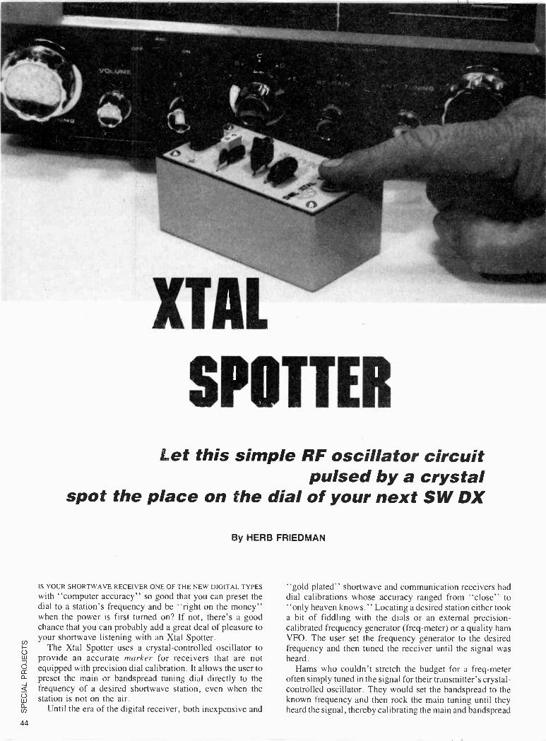
XTAL
SPOTTER Let this simple RF oscillator circuit
pulsed by a crystal spot the place on the dial of your next SW DX
By HERB FRIEDMAN
IS YOUR SHORTWAVE RECEIVER ONE OF THE NEW DIGITAL TYPES
with "computer accuracy" so good that you can preset the dial to a station's frequency and be "right on the money" when the power is first turned on? If not, there's a good chance that you can probably add a great deal of pleasure to your shortwave listening with an Xtal Spotter.
The Xtal Spotter uses a crystal -controlled oscillator to provide an accurate marker for receivers that are not equipped with precision dial calibration. It allows the user to preset the main or bandspread tuning dial directly to the frequency of a desired shortwave station, even when the station is not on the air.
Until the era of the digital receiver, both inexpensive and
"gold plated" shortwave and communication receivers had dial calibrations whose accuracy ranged from "close" to "only heaven knows." Locating a desired station either took a bit of fiddling with the dials or an external precision - calibrated frequency generator (freq-meter) or a quality ham VFO. The user set the frequency generator to the desired frequency and then tuned the receiver until the signal was heard.
Hams who couldn't stretch the budget for a freq-meter often simply tuned in the signal for their transmitter's crystal - controlled oscillator. They would set the bandspread to the known frequency and then rock the main tuning until they heard the signal, thereby calibrating the main and bandspread
PARTS LIST Resistors are 1/2 -watt, 10% unless otherwise noted
R1-270,000 ohms R2-1000 ohms
O O Connectors S01 S02
C1-68-pF 5% mica O O
02-1000-pF 5% mica C3-470-pF 04-0.01 µF
Miscellaneous Q1-NPN transistor, 2N3391. S1-Normally-open pushbutton switch B1 -9 -volt transistor battery S01-FT-243 crystal socket, JAN SSO -1, see text. S02-HC25/U crystal socket, JAN CE -25, see text. Cabinet, hardware wire, solder etc.
Note. Crystal sockets and crystals are available from JAN Crystals, 2400 Crystal Drive, FT. Myers, FL 33906. Send for free catalog before you order.
dials for a given band. Naturally, SWL's didn't have a
crystal -controlled transmitter to provide a reference frequen- cy, so finding a signal-even when the frequency was known-often was hit-or-miss.
One inexpensive idea that worked well when there were only a few "important" frequencies to monitor was the crystal controlled spotting oscillator, or Xtal Spotter as it's more frequently called. That is simply a very low power crystal oscillator that provides a marker for the receiver. The user keys the spotter and simply tunes the receiver until the signal is found.
Inside the circuit The unit shown in the photographs is a modern version of
the Xtal Spotter specifically intended to be built from junk - box parts and designed for SWL use between about 1.5 and 30 MHz. Most everything should be found lying around your
Sockets can be provided to accommodate two or more of the standard crystal holders, as shown. Naturally, you can't use two crystals at once; we plugged in two just to illustrate how the standard FT -243 and HC25/U crystals fit on the board.
R1
270K
Cl E
68pF ____1(____,
R2
1K
C4 7 .01
y
S1
yo711 I
B1 1 9V =
01
2N3391 C3
470pF
.______i o TP
C2
1000pF
T 1/8"H 14-
1 /4"
1/4" "Z" PIN FOR TP (TEST POINT)
E C B
000
O1-253391 BOTTOM VIEW
Fig. 1. SCHEMATIC DIAGRAM FOR XTAL SPOTTER uses a 250 h10 minimum transistor. Two or more crystal sockets may be
installed on the project, however, only one crystal at a time may be used in the circuit. Keep the project construction neat and clean, and there should be no problems during the first test.
shop. All you should need to buy are the crystals (and perhaps their sockets), and later we'll tell you where to get them at rock -bottom cost, usually between $2.50 and $4.
If you examine the schematic diagram in Fig. 1, you can probably think of several ways to improve the circuit. However, the circuit shown will work with just about every type of crystal you're likely to come across, regardless of the tolerance of the components used. Basically, the circuit is
uesigned to insure that the oscillator will "start" with every type of crystal when power switch Si is depressed. You can use "fundamental" crystals, or the "overtone" type; they will all start. The actual output frequency might be off a few Hz from the specified value, but you'll at least be "on frequency" regardless what crystal you use.
The test point labeled TP in Fig. 1 provides a small output sample for driving a frequency counter, just in case you want to check the precise output frequency.
To feed a frequency counter, connect the counter's hot test clip to the Z pin test point (TP) and the ground test clip to the ground end of resistor R2. Insert a crystal into either socket, depress S1,
on Xtal Spotter and let the frequency counter do all the rest!
TP
C3
C1
The entire Xtal Spotter project is assembled on a small printed - circuit board that also serves as the cover for the cabinet. Ilote that there's more than enough room to add another crystal socket or more if needed.
:x71
immora/ miimp `*. rg
SO2 A, RI '- Q1
- C2 _.'r- -- R 2
.___--C4
SMYI XTAL SPQT Sl
r"
Tips on Xtals A quick note about overtone crystals: They oscillate at
approximately one-third or one -fifth the specified frequency. Third overtone crystals were commonly used for CB. We say "approximately" because they provide the specified output frequency only when used in an "overtone -type" oscillator circuit. Used in a "standard" oscillator circuit they tend to oscillate a few hundred Hz below the calculated "base" frequency.
The least expensive crystals are military surplus. There's not too much of a demand for crystals in "large" holders, such as the FT -243, and you can often pick them up two -for - $1. Though they might be some 30 years old (or more) they are still good, and certainly worth the price.
If you can't find what you want as a surplus you can order crystals cut to your frequency from JAN Crystals, 2400
Fig. 2. CIRCUIT -BOARD TEMPLATE is shown here foil -side up and exact size. The circuit board serves as the unit's cover with all component parts except for the clip -on transistor battery.
Crystal Drive, Fort Myers, FL 33906. Their crystals are available in various holders: HC6/U, HC25/U, HC18/U, H 17/U, HC33/U and FT -243. They even sell the crystal sockets at rock -bottom prices. The two used in this article are available from JAN Crystals for 20 cents and 30 cents; that's even less than Radio Shack charges for a pack of resistors. JAN Crystals has so many different crystals and holders available that you must have their catalog before placing an order.
Construction The Xtal Spotter is built on a printed -circuit board that also
serves as the cover for a plastic experimenter's cabinet appro- ximately 21/2 x 15/8 x 4 inches. A full scale template of the foil layout is provided in Fig. 2. Any substitute for the specified transistor should work as long as the hfe is at least 250. Capacitors Cl and C2 should be 5% mica; C3 and C4 can be anything: mica, ceramic, poly, etc.
Sockets SOl and SO1 match the crystal types that you plan to use. If you only use one type of crystal, simply eliminate one socket. In the model shown, sockets for the FT -243 and HC25/U crystals were provided because they are the types most frequently used or found surplus.
Any normal -open pushbutton switch can be used for power -switch S1 . Battery B 1 is a standard 9 -volt transistor - radio type battery, which is secured by a small holder inside the cabinet. Since the current drain is only about 5 mA when operating, a standard carbon -zinc battery should last almost its shelf life.
The test point, labled TP, is a small Z pin fashioned from #20 wire or a wire -wrap terminal. The Z shape is sug- gested only because it has a little extra support for the small alligator clip of a frequency -counter's test cable.
Checkout Connect a 0-10 DC mA meter in series with one battery
connection, and without a crystal installed, depress Si, and note the current reading-which should be in the range of 4 to 6 mA. While holding S I down, insert a known good crystal. If the unit breaks into oscillation, the current will rise approx- imately 0.5 to 1 mA. If there is absolutely no rise in current, check for a wiring error.
Using the Spotter Set a shortwave receiver to the correct band and approx-
imate crystal frequency. Set the receiver's BFO to on, or set the AM/SSB selector to SSB so the BFO is on. Place the spotter near the receiver, preferably on top towards the an- tenna connection, and depress S 1. While holding S 1 on, tune the receiver until you hear the heterodyne (whistle) caused by the bfo beating against the Xtal Spotter's output. Key S 1 on and off a few times so you're certain that the beat you're hearing belongs to the spotter and not a SW station.
Counter connection If you want to check the Xtal Spotter's frequency with a
counter, set the counter to maximum sensitivity, connect the counter's ground test clip to the "ground" end of resistor R2 (nearest the edge of the PC board), and clip the counter's "hot" test clip to TP. Note that the spotter's output level is designed for the lowest possible value that will provide a dependable marker. It is not, by any means intended to overwhelm the receiver input, so connecting a wire "an- tenna" to test point TP will have virtually no affect on the Xtal Spotter's signal level. SP
FLASHMETER
FOR YOUR STROBE Measure strobe effectiveness as the pros do Measure available flash light at the subject!
MODERN 35 MM SLR CAMERAS INCLUDE SO MUCH ELECTRONIC
hardware that it's almost impossible to take a poor picture providing you're taking pictures in the sunlight, available light, or "available darkness". But, as soon as artificial illumination from a flash is needed it's a "whole 'nother ballgame." The reason is that you often must depend on film guide numbers for proper exposure, and they have no relation to the real world where the color of the walls, height of the ceiling, and depth behind the subject often make those guide numbers relatively meaningless. Even modern automatic strobes with a built-in light sensor can be fooled by the colors of the room, height of the ceiling, etc.
Then, there are extreme close ups, or macro -photography. Even autostrobes with normally accurate light sensors are often fooled when the light -to -subject distance is small. The result is overexposed, washed-out detail.
But use Flashmeter that is specifically designed for electronic flash and most difficult lighting situations are easily resolved with the proper film exposure.
Flashmeter is used in the same way as a standard incident - light meter: You place it at the subject location facing be- tween the camera and the flash-or at the camera if the flash is mounted on the camera bracket, fire the flash, and then read the required f-stop (lens opening) directly off the meter's scale. (There is no interpolation of scale reading to exposure
HERB FRIEDMAN
chart required.) Depending on the quality of components used for the project, the Flashmeter reading will hold (hangup) from one to several minutes before drift to zero causes any significant error in the reading.
The Flashmeter features meter -scale calibration in full stops from f:4.0 to f:22 for film speeds from EI 25 to EI 400, instant meter reset, and a built-in battery check. By the way, EI means Exposure Index, and in most cases is identical to the ASA rating found on all film packages. Some time ago, that was not the case. Also, some photographers use their own EI to match their equipment and studio requirements.
How it works Resistors R1, R2, and R3 together with photo -resistor PR 1
form a voltage divider across the 9 -volt power source (see Fig. 1). Part of the voltage is tapped off at FILM SPEED
potentiometer R1 and fed to capacitor Cl. Diode D1 serves primarily as a "one-way gate" so that the resistor network doesn't discharge Cl. Normally, PR1's resistance is ex- tremely high compared to the rest of the divider, so that virtually no voltage is developed at RI's tap. What voltage there is, is less than diode Dl's "breakover" rating so that no charge is applied to Cl. When the flash is set off, its light is
summed with the room's ambient light causing PR1's resis- tance to decrease sharply. That makes the voltage at RI's
SENSOR /1
GATE 2
DRAIN
BOTTOM VIEW
SK3065
1N` 1
R2
560S2
01+
PR1
G2
Q1
R1
5005? FILM
Cl ^s.i
G1 S
R3
50052 CAL
R42.7K
GATE 1
CASE, SOURCE AND SUBSTRATE
BATT 1
4 9V
S1
DPDT CENTER OFF o R5
5602, -W
1 -
0
R72.7K
5K ZERO
R8
5K 0
BAT (7?
2
o
-1" ON OFF M1
0 1mA
o 3
o
FIG. 1. SCHEMATIC DIAGRAM FOR FLASHMETER uses a high -impedance input FET to amplify charges on capacitor Cl. The capacitor's charge is made possible by the drop- ping in value of PR1 when in the presence of a bright light flash. Diode D1 allows Cl to charge through it. Cl cannot discharge, because both the diode and the gates on the FET present resistances that limits current leakage to a few microamperes. Cl will hold a charge long enough to take a reading before It begins to drift downward.
wiper rise. When the voltage rises, it exceeds D1 's "breakover" point and' the diode conducts. Current flows through D1, charging capacitor Cl.
Transistor Q1 is an insulated gate FET, whose input im- pedance is in the thousands of Megohms. It senses the vol- tage across Cl, which is dependent on the intensity of the light from the flash that reaches sensor PR1, and results in a reading on meter MI (see Fig. 1). Because of Q l's unusually high impedance, it causes no appreciable discharge of C l , so meter MI 's indication is sustained over a relatively long time period.
Photoresistor PR1 is a special high-speed type, whose color sensitivity and resistance range was specifically selected for this project. The Flashmeter will probably not work with any other photoresistor.
Construction Warning! Do not handle Ql until told to do so! If you
are unfamiliar with handling FET's, you may blow Q1 before you are ready to install it.
The Flashmeter is built into a plastic cabinet that measures approximately 31/2 x 2 x 5'/8 inches. I used a Hammond cabinet for Flashmeter shown in the photos. Hammond cabinets tend to shatter easily when mounting holes are drilled. If you aren't particularly adept at cutting holes in a "hard" plastic cabinet, substitute a "soft' plastic cabinet such as those sold by Radio Shack. They aren't as classy - looking as the Hammond's, but softer plastic is easier to work with if you don't have a drill press or a variable -speed electric drill.
All component values are critical and few substitutions may be made. (If you can't obtain the specified components or their recommended substitutions don't build the project- it won't work properly.)
Potentiometer R1, the FILM SPEED control, is particularly critical. It must be 500 ohms and it must have a linear taper. The unit shown in the photographs is a wirewound pot often found in "surplus" stores for $1 to $3. A wirewound is suggested because it's more stable and more likely to hold its setting even if handled roughly. But don't spend a fortune on the pot. If you can't get a wirewound at a decent price use a standard carbon type. If you can't obtain a 500 -ohm unit, then check out a local TV parts supplier, and see if you can
THE FIELD-EFFECT TRANSISTOR (FET) IS VERY SENSITIVE to electrostatic charge before it is installed onto the printed -circuit board. Pencil points to metal wire spring that shorts the four FET leads together. Do not remove spring from FET until after the leads have been soldered in place on the printed -circuit board and the battery is connected.
get two 1000 -ohm pots on the same control shaft (dual pots). That may be easier to find. Then, tie all three common terminals in parallel (upper end to upper end, wiper to wiper, and lower end to lower end). You now have a 500 -ohm pot with no tracking error. In fact, the resulting network of two pots may be more linear than one pot alone.
In the event you absolutely cannot obtain a 500 -ohm pot, you can use a larger size if a fixed resistor is connected in parallel with R1 across the end terminals, and the combined resistance of the pot and the resistor sums in parallel to 500 ohms. The resulting tolerance of the network is ± 10% of the expected linear tracking. There are two extra holes on the PC board for that resistor. However, bear in mind that the Film Speed calibration won't be reasonably linear, and might be all scrunched at one end if R1 isn't 500 ohms. The parallel resistance arrangement has been provided only for those builders who in no way can get a 500 -ohm pot.
Most of the circuit for the Flashmeter is assembled on a printed -circuit board (See Figs. 2 and 3) that mounts directly on the back of the meter, and the connections from the PC
2 1/2 INCHES
FIG. 2. PRINTED -CIRCUIT TEMPLATE FOR FLASHMETER is sim- ple to copy. If you prefer to lay out your own-do so, since the circuit is not critical to parts placement.
METER
S1-2,4
S1-1
BATT +
S1 6
FIG. 3. PARTS -LAYOUT DIAGRAM is shown with printed -circuit. board, foil -surface down. Large terminal circles near top of board are for meter M1 terminal holes. Refer to text for further informa- tion. Note position of FET's case tab. Your hookup should match this layout.
PARTS LIST
RESISTORS All %-watt, 10% or better unless otherwise specified R1 -500 -ohm potentiometer, linear taper, preferably wire - wound R2, R5-560 ohms R3 -500 -ohm trimmer potentiometer, flat mounting R4, R7-2700 ohms R6, R8 -5000 -ohm trimmer potentiometer, flat mounting PR1-Photoresistor, Clairex 903. CAPACITOR C1-0.1 µF Mylar or disc capacitor, rated higher than 10 volt SEMICONDUCTORS D1-1N456A Q1-MOSFET, RCA SK3065 MISCELLANEOUS BATT1-Battery, 9 -volt, type 2U6 or equivalent Ml-Meter, 0-1 mA DC, Calectro D1 -912 S1-Switch, DPDT center-off-preferably one side spring re- turn Cabinet, white dome, PC materials, knob, white transluscent jewel or dome, etc.
foils to the meter terminals are automatic when the board is secured to the meter.
The meter used must be a Calectro type D1-912 0-1 mA DC with screw -type terminals. The same meter, or a similar model was sold under different labels-among them Radio Shack. But some of the other brands changed the con- nections, substituting solder terminals for the screw con- nections. The printed -circuit board won't mate with the sol- der -type terminals. Also, doublecheck the Calectro model and make certain that it has screw terminals. At the time this article was prepared, Calectro used screw terminals, but in this day and age anything can change overnight. Don't as- sume that the meter is the same simply because the catalog number is the same.
Some similar meters had reversed meter -terminal polarity. The PC template allows for that. If you look at the printed - circuit template (Fig. 2) you'll note the two large foil pads that are the meter terminal connections. The foils to each pad are broken at X and Y. Looking at the back of the meter when held upright, if the right hand meter terminal is marked with a + , connect a jumper between the two X holes and a jumper between the two Y holes. If your meter's left hand terminal is marked with a + , connect insulated jumper wires from the top X hole to the lower Y hole, and from the upper Y hole to the lower X hole. What you must end up with is the meter's "+" terminal connected directly to Q1 's "s" terminal.
Make the PC board using the template in Fig. 2 and put the numbered markings on your board exactly as shown on the template. Final assembly will be confusing without the numbers because they match connections shown in the schematic diagram. Note that the template has a small dash representing QI's tab, and also a symbol to indicate diode Dl's polarity.
Working with a FET Carefully unpack Q 1 and look at the base of the leads
where they enter the transistor. You will find a shorting wire wrapped around the leads. DON'T REMOVE THIS SHORTING
WIRE UNTIL THE ENTIRE PROJECT IS COMPLETED. Q t iS a MOS-
PHOTOTRANSISTOR R1 LEADS MUST BE EXTENDED prior to installation on the printed -circuit board. Slip a sleeve insulator over one of the leads to avoid their accidental shorting. Use bare, solid hookup wire and a drop of solder.
FET, and is very susceptible to static electricity prior to installation without the shorting wire across the leads. One static "shot" and Q1 is "blown." The shorting wire is removed after the unit is wired and the battery has been installed.
Mount all components, including the connecting wires on the PC board (see Fig. 3), but don't install the meter. Either use color -coded wires to match the numbered connection holes, or tag each wire with an adhesive label.
Set the board aside for the moment and mount all front - panel parts. Switch S 1 is a DPDT, center -off toggle device; preferably spring -return from one side. Use the spring -return side for the BAT (battery test) position. Mount potentiometer RI 1'/4 inches from the bottom of the cabinet. Mount resistive sensor PC1 and switch S1 on a line 2 inches from the bottom (check the photos).
Resistive sensor PR1 must look into a white "light in- tegrator". The integrator in the unit shown uses the white lamp - holder from a set of five colored holders supplied with a blister -packaged Muralite low -voltage panel lamp kit. You can substitute the dome or cover from a white pilot -lamp assembly. In fact, any translucent white dome can be used.
When all panel components, including the meter, have been installed, mount the PC board on the meter terminals, connect the wires from the board to the switch and pot, and then install sensor PC1. To install PC1, first solder a 1 -inch solid wire to each of PC's leads and place a' -inch length of insulation over one lead. Slip PC1 into the white integrator dome, slide its wires into the PC -board holes, and then position PC1 before soldering, so that it is at least 1/4 inch back from the front of the integrator. PC1 must look "into" the integrator; if it's flush with the front of the integrator it won't read light coming from the sides correctly.
FLASHMETER
ORIGINAL METER SCALE f -STOP
1.0 22 0.8 16 0.65 11 0.45 8 0.27 5.6 0.13 4
FIG. 4. AUTHOR'S FLASHMETER METER SCALE LAYOUT is provided here to assist you in either making your own scale or copying the above. A carefully drawn and Inked scale art will make your unit very handsome and give it the pro look.
The meter scale You can either recalibrate the supplied meter scale, or
make an entirely new scale using the full-scale template (see Fig. 4). If you want simply to recalibrate the existing scale, use the conversion values in the chart, which shows the f-stop value for the original scale calibrations. If you decide to make an entirely new scale, do it this way: First, create the new scale on white paper. You can do that either by making a Xerox copy of the template, or by using the template itself.
To install the new scale, use a small screwdriver slipped under the top of the meter cover to gently pop the cover off the meter. Taking extra care not to damage the pointer, remove the two Phillips screws that hold the scale and slide it out from under the point. Slide, don't lift. Lifting will damage the pointer. Flip the scale over so the metal side is up. Cut out the new scale (or Xerox copy), punch out the screw holes from the new paper scale, and apply a very thin layer of rubber cement to the back. Then position the new scale on the metal scale, smooth out the bubbles, and allow the cement to dry. Slide the new scale under the meter pointer, insert the screws (don't let them fall into the meter), and install the cover.
Powering up Make certain S 1 is in the center OFF position, install the
battery, and carefully pull the shorting wire off Q1. Make sure none of Q1 's leads are touching.
Set R1 fully counterclockwise and install a knob with the pointer at 7 o'clock. If the control is rotated fully clockwise, the pointer should be at 5 o'clock. Fudge the knob's adjust- ment until its pointer falls equally on either side of the 6 o'clock position when the knob is rotated to both extreme settings.
Set S 1 to BAT and adjust trimmer pot R8 until the meter pointer falls directly on the scale calibration marked B(atter- y); which is also the f:22 mark. Then flip S1 down to ON and adjust trimmer pot R6 so that the meter pointer falls directly over the extreme left calibration, which is really the original "0" calibration. Set S 1 to the center or OFF position. Then
(Continued on page 98)
LIGHT INTEGRATOR is a translucent white lampholder which will house photoresistor PR1. Prior to soldering the leads of PR1. be sure that the top of PR1 is 'i4 inch from inside top of lamphol- der. That should place the photoresistor about flush with the surface of the printed -circuit board. Note that light integrator is cemented in place.
50
SMART
POWER SUPPLY Why use smoke signals to spot troubles? Disconnect the regulated power supply
before its circuit elements go poof! ALAN S. COBB
HAVE YOU EVER MADE THE CONNECTIONS ON A BREADBOARD project and noticed smoke rising from your power supply or other components, as a short circuit fries them? Then get smart-not you, but your power supply! This "smart" pow- er supply was designed after the author blew too many fuses and rectifiers because of accidental shorts during TTL pro- totyping.
The Smart Power Supply is like a circuit breaker, except that it is much faster and can be very accurately pre-set to shut down at an exact level of load current. Conventional circuit breakers aren't as precise. Other units may take from 5 to 30 seconds to open when the load current exceeds 200% of its rating. A lot of damage can take place in those smoking seconds. Although the 7805 regulator chip used on most 5 -volt supplies has internal circuits to shut itself down when excessive current causes overheating, if you're using enough heatsink the process is a gradual one, taking much longer than the Smart Power Supply.
Construction Most of the parts involved can be purchased at neighbor-
hood or mail order outlets. To simplify the design and reduce the cost, you could leave out the 250 mA low range by only using the high range's 200,000 -ohm feedback trimpot, R5
(see Fig. 1). You could leave out the meter, too, although it is
helpful to see how changes in your breadboard experiments affect the current drawn from the supply.
Although other chassis can be used, one with a sloping frontpanel makes the meter and indicator LED's easier to read. The author fabricated his own from sheet 18 -gauge aluminum. After laying out the pattern on the metal, cut it out with a saber saw. The required bends were made by using pieces of/winch aluminum, plate and "C" clamps to hold the sheet metal to the bench while the folds were formed with hand pressure and a lot of hammering. After bending and drilling the chassis, immerse it in a solution of 1/2 -can of Drano (lye) to 3 gallons of water for several hours to give the aluminum a satin finish. It is important to submerge the aluminum completely in the solution. If part remains ex- posed, a crusty streak will form where the metal first meets the liquid. After the etching, follow with a complete rinse and scrub down the metal to remove all lye. Next apply press -on transfer letters and spray on several coats of clear polyurethane finish over several days to protect the lettering. Instead of rubber feet for the enclosure use two 6 -inch long strips of '/cinch self -sticking weather strip on the bottom. The final step in chassis preparation is to add a handle on top to make the supply easier to carry.
Most of the electronic components are mounted on a
standard 6 x 2 -inch circuit board with the same pattern as a
Ti
S1
IC3, IC4 7400,LM324
T1
12.6VCT 1.2A
IC1, 1C2
7805
G
LEDI Y
R1
18052
F1
1/2A
S1
POWER
BR1
ICI 7805
TO 1C4-4 AND IC3-14I A-- i N.O.
C
Cl ..".'4700/35V
R2
15K
C4
T1.0µF
®
R4 LOW
1MEG - 3P
R5
200 K
3
2
o CUTOFF
TOPIN7 R3 IC3
0.152
LEVEL
1/4 7400
0.1
M1
RY1
R7 .
56K
12
13
R8
15K
0.1
2N1305 (SEE PARTS LIST)
eR9 150K
14 5
1/47400 6
1/4 7400
FROM IC3-o
1310
150K
R12 68052
1/4 LM324
11
q°S3 RESET
10
SCHEMATIC DIAGRAM FOR THE SMART POWER SUPPLY is as simple as its name. After the coarse DC voltage is rectified by diode bridge BR1, two separate regulated 5-VDC supplies thrive off it. One 5-VDC supply, developed by IC1, powers the current -sensing circuit and cut-out relay RY1. The remaining 5-VDC supply is switched on and off by the action of the relay and RESET switch S3.
Cl
M1
CIRCUIT
BOARD
S2
LED2
S3
J1
J2
PARTS LOCATION LAYOUT FOR THE SMART POWER SUPPLY. Nothing is critical here, so let neatness and cost determine best practical way to proceed with project.
conventional 6 x 2 -inch solderless breadboard. The circuit board was mounted on the top chassis section (see photo) with 1 -inch 4-40 machine screws and 3/4 -inch spacers. The foil side of the card is exposed so that the wires to the off -board components can be easily soldered in place after everything else is installed. Most of the on -board com- ponents can be mounted on the underside (non -foil side) of this card, while Cl and the three trimpots (R4, R5, and R6) are put on the foil side for easy access and adjustment.
The two 7805 regulators (IC1 and IC2) are bolted to the back of the chassis close to the board. Thus the entire enclo-
sure acts as a heat sink. Be sure to mount C4 and C5 right on top of the 7805's with short leads.
How the circuit works The basic circuit is the same as a regular fused, 1.0 -amp
power supply. (See Fig. 1.) The "intelligence" circuitry consists of two ICs, a 7400 (IC3), and a LM324 (IC4). The LM324 is a quad Op -Amp package that can be powered by a single 5 -volt supply rather than the normal dual supplies. As with the other control logic, it draws power through its own 7805 regulator (IC1), so the relay doesn't have to be put between the load and primary regulator (IC2) causing a voltage drop.
Both inputs (pins 9 and 10) on IC4 unused Op -Amp should be grounded to reduce noise, but do not ground the output (pin 8). To save a little current, ground the inputs (pins 4, 5, 12, and 13) on IC3 unused gates and leave their outputs unconnected.
The DC -load current passes through resistor R3. The vol- tage drop across R3 is amplified by the first Op -Amp, IC3-a. That amplified voltage is fed to the comparator IC3-b. When the amplified voltage goes above the comparator's reference voltage,its output (pin 14) snaps low. The second comparator (IC3-c) makes that snap action even more crisp. When its non -inverting input (pin 5) goes lower than the reference (pin 6), its output goes low (pin 7). That output of the second comparator is fed to the latch (gates IC4-a and IC4-b). When pin 1 of IC3-a goes low, the output of gate IC4-b (pin 8) will go low; that causes transistor Q1 to conduct and open the relay cutting off the load current. The latch will hold pin 8 low even after pin 1 of IC3-a goes high again. If there were no latch circuit here, the system would cycle continuously, first
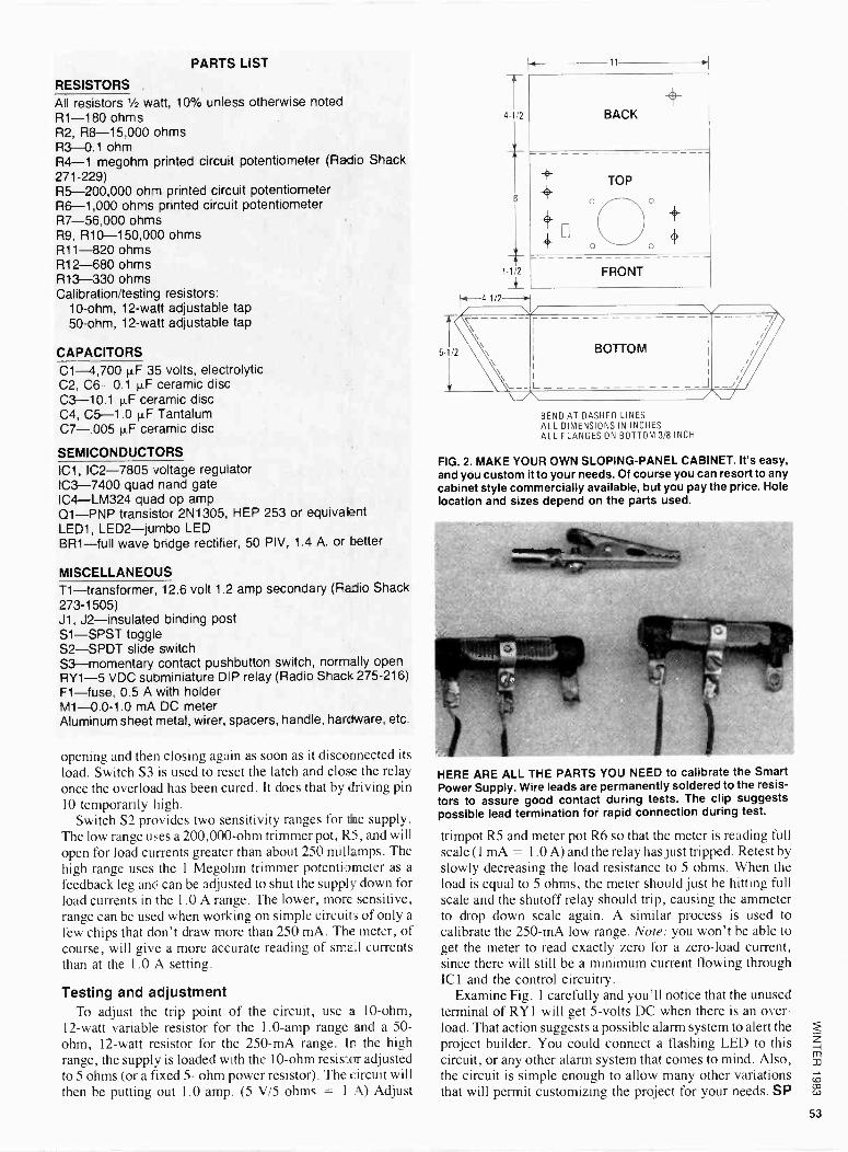
PARTS LIST
RESISTORS ,
All resistors 1/2 watt, 10% unless otherwise noted R1-180 ohms R2, R8-15,000 ohms R3 0.1 ohm R4-1 megohm printed circuit potentiometer (Radio Shack 271-229) R5-200,000 ohm printed circuit potentiometer R6-1,000 ohms printed circuit potentiometer R7-56,000 ohms R9, R10-150,000 ohms R11-820 ohms R12-680 ohms R13-330 ohms Calibration/testing resistors:
10 -ohm, 12 -watt adjustable tap 50 -ohm, 12 -watt adjustable tap
CAPACITORS C1-4,700 µF 35 volts, electrolytic C2, C6-0.1 µF ceramic disc C3-10.1 µF ceramic disc C4, C5-1.0 µF Tantalum C7-.005 µF ceramic disc
SEMICONDUCTORS IC1, IC2-7805 voltage regulator IC3-7400 quad nand gate IC4-LM324 quad op amp Q1-PNP transistor 2N1305, HEP 253 or equivalent LED1, LED2-jumbo LED BR1-full wave bridge rectifier, 50 PIV, 1.4 A. or better
MISCELLANEOUS T1-transformer, 12.6 volt 1.2 amp secondary (Radio Shack 273-1505) J1, J2-insulated binding post Sl-SPST toggle S2-SPDT slide switch S3-momentary contact pushbutton switch, normally open RY1-5 VDC subminiature DIP relay (Radio Shack 275-216) Fl-fuse, 0.5 A with holder M1-0.0-1.0 mA DC meter Aluminum sheet metal, wirer, spacers, handle, hardware, etc.
opening and then closing again as soon as it disconnected its load. Switch S3 is used to reset the latch and close the relay once the overload has been cured. It does that by driving pin 10 temporarily high.
Switch S2 provides two sensitivity ranges for tile supply. The low range uses a 200,000 -ohm trimmer pot, RS, and will open for load currents greater than about 250 millamps. The high range uses the 1 Megohm trimmer potentiometer as a
feedback leg and can be adjusted to shut the supply down for load currents in the 1.0 A range. The lower, more sensitive, range can be used when working on simple circuits of only a
few chips that don't draw more than 250 mA. The meter, of course, will give a more accurate reading of small currents than at the 1.0 A setting.
Testing and adjustment To adjust the trip point of the circuit, use a 10 -ohm,
12 -watt variable resistor for the 1.0 -amp range and a 50 - ohm, 12 -watt resistor for the 250 -mA range. In the high range, the supply is loaded with the 10 -ohm resistor adjusted to 5 ohms (or a fixed 5- ohm power resistor). The circuit will then be putting out 1.0 amp. (5 V/5 ohms = 1 A) Adjust
4-1/2
11
4- BACK
TOP
o
o
o
FRONT
BEND AT DASHED LINES ALL DIMENSIONS IN INCHES ALL FLANGES ON BOTTOM 3/8 INCH
FIG. 2. MAKE YOUR OWN SLOPING -PANEL CABINET. It's easy, and you custom it to your needs. Of course you can resort to any cabinet style commercially available, but you pay the price. Hole location and sizes depend on the parts used.
HERE ARE ALL THE PARTS YOU NEED to calibrate the Smart Power Supply. Wire leads are permanently soldered to the resis- tors to assure good contact during tests. The clip suggests possible lead termination for rapid connection during test.
trimpot R5 and meter pot R6 so that the meter is reading full scale (1 mA = 1.0 A) and the relay has just tripped. Retest by slowly decreasing the load resistance to 5 ohms. When the load is equal to 5 ohms, the meter should just be hitting full scale and the shutoff relay should trip, causing the ammeter to drop down scale again. A similar process is used to calibrate the 250 -mA low range. Note: you won't be able to get the meter to read exactly zero for a zero -load current, since there will still be a minimum current flowing through 1C l and the control circuitry.
Examine Fig. 1 carefully and you'll notice that the unused terminal of RY I will get 5 -volts DC when there is an over- load. That action suggests a possible alarm system to alert the project builder. You could connect a flashing LED to this circuit, or any other alarm system that comes to mind. Also, the circuit is simple enough to allow many other variations that will permit customizing the project for your needs. SP
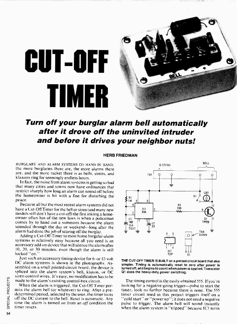
CUT-OFF
TIMER Turn off your burglar alarm bell automatically
after it drove off the uninvited intruder and before it drives your neighbor nuts!
HERB FRIEDMAN
BURGLARY AND ALARM SYSTEMS GO HAND IN HAND. the more burglaries there are, the more alarms there are, and the more racket there is as bells, sirens, and klaxons ring for seemingly endless hours.
In fact, the noise from alarm systems is getting so bad that many cities and towns now have ordinances that restrict sharply how long an alarm can sound off before the homeowner is hit with a fine for disturbing the peace.
Because all but the most recent alarm systems did not have a Cut -Off Timer for the bell or siren (and many new models still don't have a cut-off) the first inkling a home- owner often has of the new laws is when a policeman comes by to hand out a summons because the alarm sounded through the day or weekend-long after the alarm had done the job of scaring off the burglar.
Adding a Cut -Off -Timer to most home burgular-alarm systems is relatively easy because all you need is an accessory add-on device that will silence the alarm after 10, 20, or 30 minutes, even though the alarm is still locked "on."
Just such an accessory timing device for 6- or 12 -volt DC alarm systems is shown in the photographs. As- sembled on a small printed -circuit board, the device is spliced into the alarm system's bell, klaxon, or DC siren -control wires. It's easy; no modification has to be cn
i- made to the alarm's existing control -box circuit. When the alarm is triggered, the Cut -Off Timer per-
(?) mits the alarm bell (or whatever) to ring. After a pre- eL determined period, selected by the user, the timer turns
off the DC current to the bell. Reset is automatic. Any w time the alarm is turned on from an off condition the
timer resets.
R1
1M 4
6
TB1
.1
6-12VDC BELL
o o
2
Cl loo
T SEE TEXT
IC1 555
3
C2 T.01
1 4
ICI TOP
R2
390
0
BCE Q1
o o
THE CUT-OFF TIMER IS BUILT on a printed -circuit board that also simpler. Timing is automatically reset to zero after power is turned off, and begins to count when power is applied. Transistor Gil does the heavy-duty power switching.
The timing control is the easily -obtained 555. If you're looking for a negative -going trigger-pulse to start the timer, look no farther because there is none. The 555 timer circuit used in this project triggers itself on a -cold start" or "power up"; it does not need a negative pulse to trigger. The alarm bell will sound instantly when the alarm system is "tripped" because IC 1 turns
54
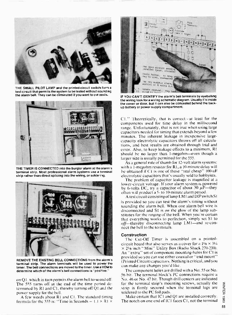
THE SMALL PILOT LAMP and the printed -circuit switch form a
test circuit that permits the system to be tested without sounding the alarm bell. They can be eliminated if you want to cut costs.
THE TIMER IS CONNECTED into the burglar alarm at the alarm's terminal strip. Most professional alarm systems use a terminal strip rather than direct splicing into the wiring, or soldering.
REMOVE THE EXISTING BELL CONNECTIONS from the alarm's terminal strip. The alarm terminals will be used to power the timer. The bell connections are moved to the timer. Use a VOM to determine which of the alarm's bell connections is "positive."
on Q l . which in turn permits the alarm bell to sound off. The 555 turns off at the end of the time period de- termined by R 1 and Cl, thereby turning off Q 1 and the power supply for the bell.
A few words about RI and Cl. The standard timing formula for the 555 is: "Time in Seconds = 1.1 x R l x
,(rra.,>.,
,argl- it senaLu) Prot. circuit)
,an,ic RuttOn, is
'aY he ur*d, ronnect«á P ar any aedih.e alarm,
.urkfnI ont, vol ,. ta t'.
IF YOU CAN'T IDENTIFY the alarm's bell terminals by eyeballing the wiring look for a wiring schematic diagram. Usually it's inside the cover or door, but it can also be concealed behind the back- up battery or power supply compartment.
Cl." Theoretically, that is correct-at least for the components used for time delay in the millisecond range. Unfortunately, that is not true when using large capacitors needed for timing that extends beyond a few minutes. The inherent leakage in inexpensive large - capacity electrolytic capacitors throws off all calcula- tions, and best results are obtained through trial and error. Also, to keep leakage effects to a minimum, Rl should be no larger than 1-megohm-even though a larger size is usually permitted for the 555.
As a general rule of thumb for 12 -volt alarm systems: with a 1-megohm resistor for R1, a 10 -minute delay will be obtained if Cl is one of those "real cheap" 100-uF electrolytic capacitors that's usually sold to hobbyists.
The problem of capacitor leakage is magnified at a lower -circuit voltage. If your alarm system is powered by 6 -volts DC, try a capacitor of about 30 µF-they often will product a 5- to 10 -minute alarm period.
A test circuit consisting of lamp LM 1 and DIP switch S 1
is provided so you can test the alarm's timing without sounding the alarm bell. When one alarm bell wire is disconnected and S 1 is on the glow of the lamp sub- stitutes for the ringing of the bell. When you're certain that everything works to perfection, simply set S 1 to off-thereby disconnecting lamp LM 1-and re -con- nect the bell to the terminals.
Construction The Cut -Off Timer is assembled on a printed -
circuit board that also serves as a cover for a It/s x 31/4
x 2t/s inch "Mini" Utility Box (Radio Shack 270-230). An "extra" set of component mounting -holes for CI is provided so you can use either coaxial or "end mount" (Printed Circuit) capacitors. Nothing is critical, and you can make any changes you'd like.
The component holes are drilled with a No. 55 or No. 56 bit. The terminal block's PC connections require a No. 46 or No. 47 bit. Though drill centers are indicated for the terminal strip's mounting screws, actually the strip is firmly secured when the terminal lugs are soldered to the PC foil pads.
Make certain that IC 1 and Q 1 are installed correctly. The notch on one end of IC 1 faces Cl, not the terminal
55
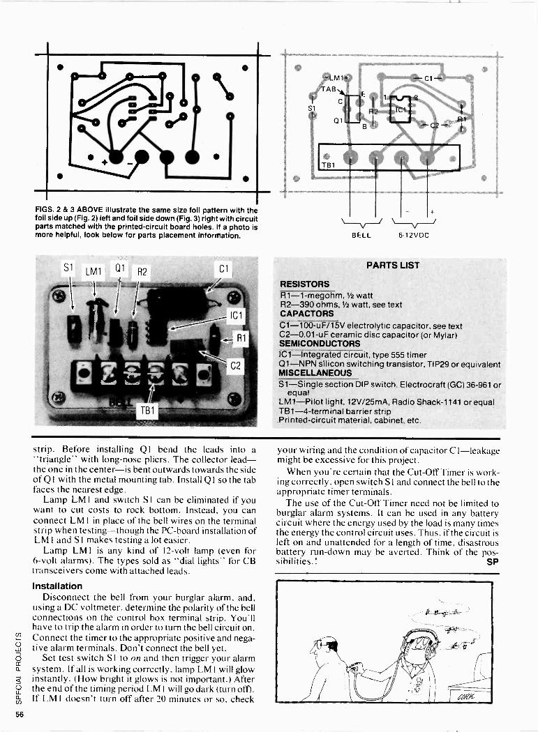
I
<reg°;14,1
FIGS. 2 & 3 ABOVE illustrate the same size foil pattern with the foil side up (Fig. 2) left and foil side down (Fig. 3) right with circuit parts matched with the printed -circuit board holes. If a photo is more helpful, look below for parts placement information.
S1 LM1 Q1 R2 Cl
BELL 6-12VDC
PARTS LIST
RESISTORS R1-1-megohm, 1/2 watt R2-390 ohms, 1/2 watt, see text CAPACTORS C1-100-uF/15V electrolytic capacitor, see text C2-0.01-uF ceramic disc capacitor (or Mylar) SEMICONDUCTORS 101-Integrated circuit, type 555 timer Q1-NPN silicon switching transistor, TIP29 or equivalent MISCELLANEOUS Sl-Single section DIP switch. Electrocraft (GC) 36-961 or
equal LM1-Pilot light, 12V/25mA, Radio Shack -1141 or equal TB1-4-terminal barrier strip Printed -circuit material, cabinet. etc.
strip. Before installing Q1 bend the leads into a "triangle" with long -nose pliers. The collector lead- the one in the center-is bent outwards towards the side of Q1 with the metal mounting tab. Install Q I so the tab faces the nearest edge.
Lamp LM 1 and switch S I can be eliminated if you want to cut costs to rock bottom. Instead, you can connect LM I in place of the bell wires on the terminal strip when testing-though the PC -board installation of LM I and S I makes testing a lot easier.
Lamp LM I is any kind of 12 -volt lamp (even for 6 -volt alarms). The types sold as "dial lights" for CB transceivers come with attached leads.
Installation Disconnect the bell from your burglar alarm, and,
using a DC voltmeter, determine the polarity of the bell connections on the control box terminal strip. You'll have to trip the alarm in order to turn the bell circuit on. Connect the timer to the appropriate positive and nega- tive alarm terminals. Don't connect the bell yet.
Set test switch S1 to on and then trigger your alarm system. If all is working correctly, lamp LM I will glow instantly. (How bright it glows is not important.) After the end of the timing period LM I will go dark (turn off). If LM I doesn't turn off after 20 minutes or so. check
your wiring and the condition of capacitor C I-leakage might be excessive for this project.
When you're certain that the Cut -Off Timer is work- ing correctly, open switch SI and connect the bell to the appropriate timer terminals.
The use of the Cut -Off Timer need not be limited to burglar alarm systems. It can be used in any battery circuit where the energy used by the load is many times the energy the control circuit uses. Thus, if the circuit is left on and unattended for a length of time, disastrous battery run-down may be averted. Think of the pos- sibilities. ! SP
60R% ..
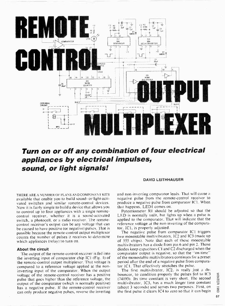
REM
CO
COMPARATOR
ARIZED TIC
LOAD
16 15 14 13 12 11 110
EXFEMIAL CIRCUIT
o t
t I 1
t 1
¡ c.V L n1
BUS 3
iCl 741113
CO (MITE
V 52
1M
M -4N-
1C2
$SS
DEBOUNCER
C31/IF c: rV R3
O 170K
10N- T 1µF
8 f7 6 5
IC3 565
DE LAY'154181 TO R
ICS 74368
BUS DRIVER
C7
.051F
BUS 4
UT
ER Turn on or off any combination of four electrical appliances by electrical impulses, sound, or light signals!
THERE ARE A NUMBER OF PLANS AND COMPONENT KITS
available that enable you to build sound- or light -acti- vated switches and similar remote -control devices. Now it is fairly simple to build a device that allows you to control up to four appliances with a single remote - control receiver, whether it is a sound -activated switch, a photocell, or a radio receiver. The remote - control receiver's output can be any voltage that can be caused to have positive (or negative) pulses. That is
possible because the remote -control output multiplexer counts the number of pulses it receives to determine which appliances (relay) to turn on.
About the circuit The output of the remote -control receiver is fed into
the inverting input of comparator chip ICI (Fig. 1) of the remote -control output multiplexer. That voltage is
compared to a reference voltage applied at the non - inverting input of the comparator. When the output voltage of the remote -control receiver has a positive pulse that goes higher than the reference voltage, the output of the comparator (which is normally positive) has a negative pulse. If the remote -control receiver can only produce negative pulses, reverse the inverting
DAVID LEITHHAUSER
and non -inverting comparator leads. That will cause a negative pulse from the remote -control receiver to produce a negative pulse from comparator IC 1. When that happens, LEDI comes on.
Potentiometer R1 should be adjusted so that the LED is normally unlit, but lights up when a pulse is
applied to the comparator. That will indicate that the reference voltage at the non -inverting of the compara- tor, IC1, is properly adjusted.
The negative pulse from comparator IC 1 triggers two monostable multivibrators, IC2 and IC3 (made up of 555 chips). Note that each of these monostable multivibrators has a diode from pin 6 and pin 2. Those diodes keep capacitors CI and C2 discharged when the comparator output is negative, so that the "on time" of the monostable multivibrators continues for a preset period after the end of a negative pulse from compara- tor IC I. That effectively stretches the pulse.
The first multivibrator, IC2, is really just a de - bouncer, to condition properly the pulses fed to IC3 (74193). Its time constant is very short. The second multivibrator, IC3, has a much longer time constant (about 3 seconds) and serves two purposes. First, on the first pulse it clears IC4 to zero so that it can begin
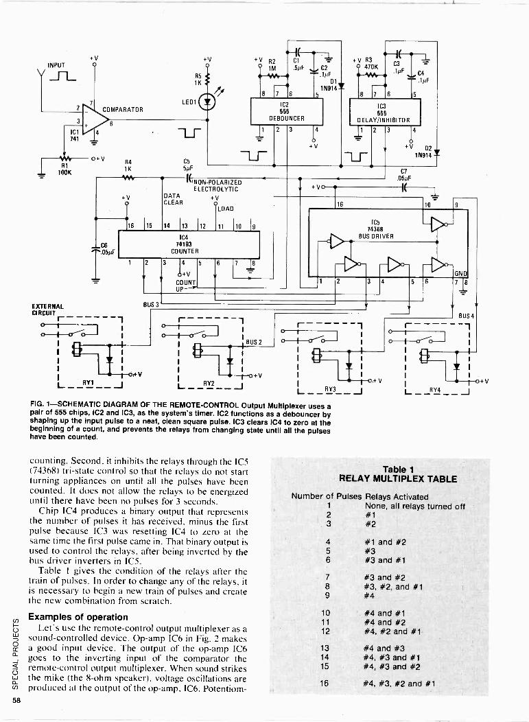
+V INPUT O V11_
3
IC1
741
R1
100K
EXTERNAL CIRCUIT
o o
7
COMPARATOR
o+V
+V
R5
1K
LEDI
R4 1K
C5
5µF
+V o
_C6 .05µF
3 I4
oI+V
COUNT UP'
5
+Vo -6 C7
.05µF
16 10
IC5 74368
BUS DRIVER
GND
BUS 3
o r------ 1 ,
o o --o BUS2
16 15
DATA CLEAR
+V R2 Cl -L.
O 1M 5µF Z C2
-.M/V- D1
1 N9141 8 7 6 5
IC2 555
DEBOUNCER
2 3
+V
+V R3 C3 0 470K .1µF C4
.1µF
8 7 6 5
IC3
555 DELAY/INHIBITOR
2 3 I4
+V D2
1N914 -Y-
Ki NON -POLARIZED ELECTROLYTIC
+V
LOAD
14 113 112 >> 110
IC4 74193
COUNTER
9
o+V
o'0
L RY3
FIG. 1-SCHEMATIC DIAGRAM OF THE REMOTE -CONTROL Output Multiplexer uses a pair of 555 chips, IC2 and IC3, as the system's timer. IC2 functions as a debouncer by shaping up the input pulse to a neat, clean square pulse. IC3 clears IC4 to zero at the beginning of a count, and prevents the relays from changing state until all the pulses have been counted.
l
t
l
t oriv L RY1 J L RY2 J
counting. Second, it inhibits the relays through the IC5 (74368) tri -state control so that the relays do not start turning appliances on until all the pulses have been counted. It does not allow the relays to be energized until there have been no pulses for 3 seconds.
Chip IC4 produces a binary output that represents the number of pulses it has received, minus the first pulse because IC3 was resetting IC4 to zero at the same time the first pulse came in. That binary output is used to control the relays, after being inverted by the bus driver inverters in IC5.
Table I gives the condition of the relays after the train of pulses. In order to change any of the relays, it is necessary to begin a new train of pulses and create the new combination from scratch.
Examples of operation Let's use the remote -control output multiplexer as a
sound -controlled device. Op -amp IC6 in Fig. 2 makes a good input device. The output of the op -amp IC6 goes to the inverting input of the comparator the remote -control output multiplexer. When sound strikes the mike (the 8 -ohm speaker), voltage oscillations are produced at the output of the op -amp, IC6. Potentiom-
I
J o
0%
71
BUS 4
L RY4
Table 1
RELAY MULTIPLEX TABLE
o+V
J
Number of Pulses Relays Activated 1 None, all relays turned off 2 #1 3 #2
4 #1 and #2 5 #3 6 #3 and #1
7 #3 and #2 8 #3, #2, and #1 9 #4
10 #4 and #1 11 #4 and #2 12 #4,#1 and #1
13 #4 and #3 14 #4, #3 and #1 15 #4, #3 and #2
16 #4, #3, #2 and #1
58
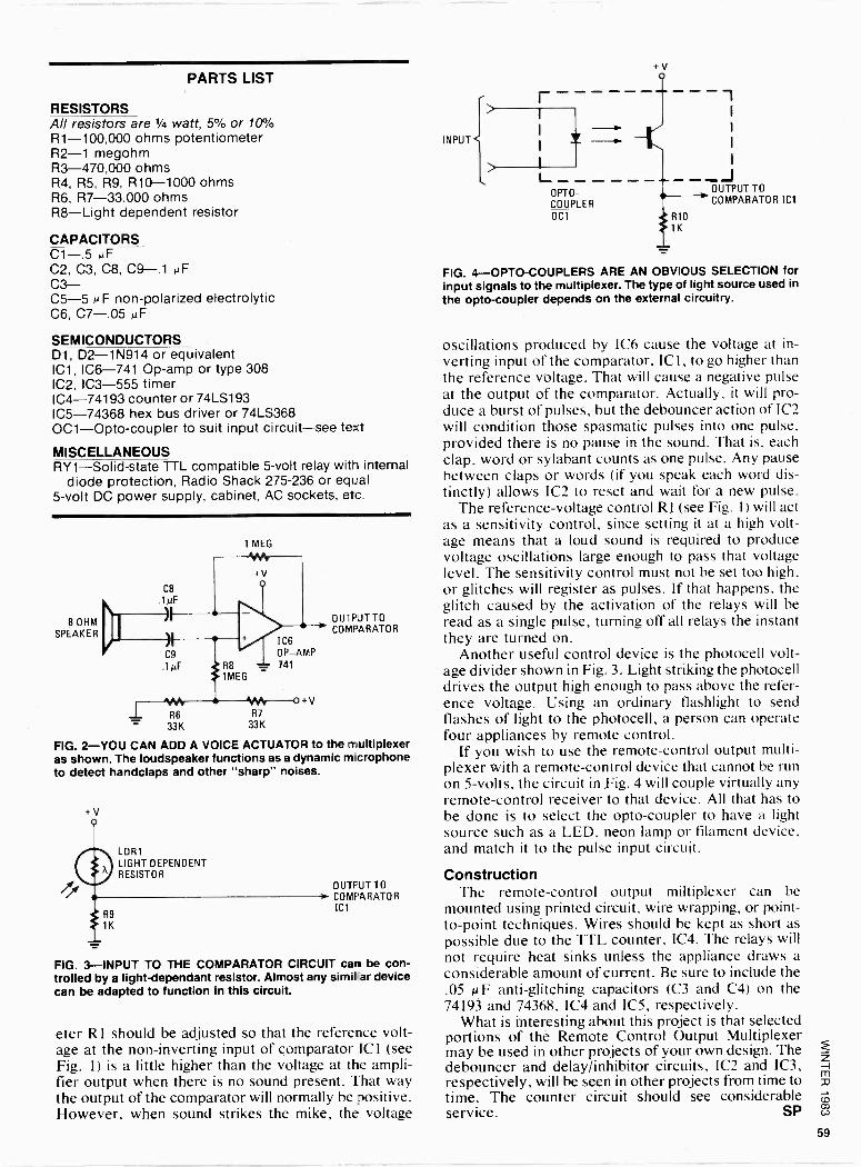
PARTS LIST
RESISTORS All resistors are 1/4 watt, 5% or 10% R1-100,000 ohms potentiometer R2-1 megohm R3-470,000 ohms R4. R5, R9, R10-1000 ohms R6. R7-33,000 ohms R8-Light dependent resistor
CAPACITORS C1-.5 uF C2, C3, C8, C9-.1 u F
C3- 05-5 u F non -polarized electrolytic C6, C7-.05 uF
SEMICONDUCTORS D1, D2 -1N914 or equivalent IC1, IC6-741 Op -amp or type 308 IC2, IC3-555 timer IC4-74193 counter or 74LS193 IC5-74368 hex bus driver or 74LS368 OC1-Opto-coupler to suit input circuit-see text
MISCELLANEOUS RY1-Solid-state TTL compatible 5 -volt relay with internal
diode protection, Radio Shack 275-236 or equal 5 -volt DC power supply, cabinet, AC sockets, etc.
8 OHM SPEAKER
1 MEG
CB
1µF
C9
.1µF t RE
>1MEG
IC6 OP -AMP
_ 741
w. w` R6 R7
33K 33K
o+V
OUTPUT TO COMPARATOR
FIG. 2-YOU CAN ADD A VOICE ACTUATOR to the multiplexer as shown. The loudspeaker functions as a dynamic miicrophone to detect handclaps and other "sharp" noises.
LORI LIGHT DEPENDENT RESISTOR
R9
1K
OUTPUT TO
> COMPARATOR IC1
FIG. 3-INPUT TO THE COMPARATOR CIRCUIT can be con- trolled by a light -dependant resistor. Almost any similar device can be adapted to function in this circuit.
eter R1 should be adjusted so that the reference volt- age at the non -inverting input of comparator IC1 (see Fig. 1) is a little higher than the voltage at the ampli- fier output when there is no sound present. That way the output of the comparator will normally be positive. However, when sound strikes the mike, the voltage
INPUT
r
L OPTO- COUPLER OC1 R10
1K
1
I
_J OUTPUT TO
COMPARATOR ICI
FIG. 4-OPTO-COUPLERS ARE AN OBVIOUS SELECTION for input signals to the multiplexer. The type of light source used in
the opto -coupler depends on the external circuitry.
oscillations produced by IC6 cause the voltage at in- verting input of the comparator, ICI, to go higher than the reference voltage. That will cause a negative pulse at the output of the comparator. Actually, it will pro- duce a burst of pulses, but the debouncer action of IC2 will condition those spasmatic pulses into one pulse, provided there is no pause in the sound. That is, each clap, word or sylabant counts as one pulse. Any pause between claps or words (if you speak each word dis- tinctly) allows IC2 to reset and wait for a new pulse.
The reference -voltage control RI (see Fig. 1) will act as a sensitivity control, since setting it at a high volt- age means that a loud sound is required to produce voltage oscillations large enough to pass that voltage level. The sensitivity control must not be set too high, or glitches will register as pulses. If that happens, the glitch caused by the activation of the relays will be read as a single pulse, turning off all relays the instant they are turned on.
Another useful control device is the photocell volt- age divider shown in Fig. 3. Light striking the photocell drives the output high enough to pass above the refer- ence voltage. Using an ordinary flashlight to send flashes of light to the photocell, a person can operate four appliances by remote control.
If you wish to use the remote -control output multi- plexer with a remote -control device that cannot be run on 5 -volts, the circuit in Fig. 4 will couple virtually any remote -control receiver to that device. All that has to be done is to select the opto -coupler to have a light source such as a LED, neon lamp or filament device, and match it to the pulse input circuit.
Construction The remote -control output miltiplexer can be
mounted using printed circuit, wire wrapping, or point- to-point techniques. Wires should be kept as short as possible due to the TTL counter, IC4. The relays will not require heat sinks unless the appliance draws a considerable amount of current. Be sure to include the .05 µ F anti-glitching capacitors (C3 and C4) on the 74193 and 74368, IC4 and IC5, respectively.
What is interesting about this project is that selected portions of the Remote Control Output Multiplexer may be used in other projects of your own design. The debouncer and delay/inhibitor circuits, IC2 and IC3, respectively, will be seen in other projects from time to time. The counter circuit should see considerable service. SP
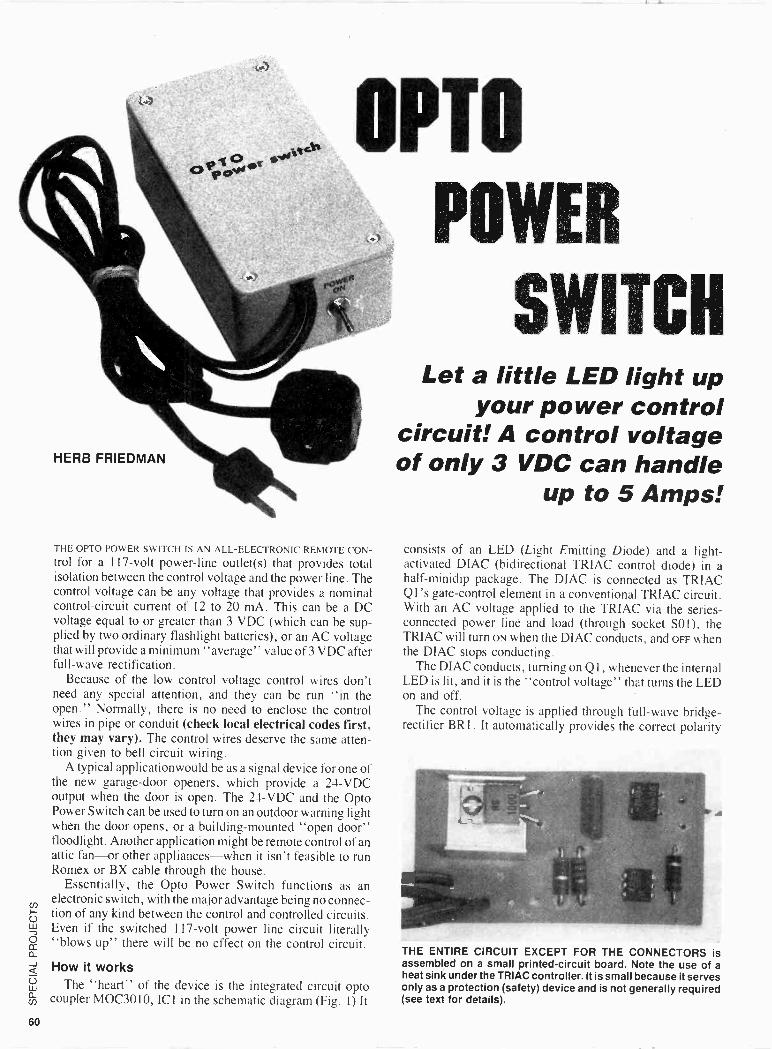
OPTO
POWER
SWITCH
HERB FRIEDMAN
THE OPTO POWER SWITCH IS AN ALL -ELECTRONIC REMOTE CON- trol for a 117 -volt power -line outlet(s) that provides total isolation between the control voltage and the power line. The control voltage can be any voltage that provides a nominal control -circuit current of 12 to 20 mA. This can be a DC voltage equal to or greater than 3 VDC (which can be sup- plied by two ordinary flashlight batteries), or an AC voltage that will provide a minimum "average" value of 3 VDC after full -wave rectification.
Because of the low control voltage control wires don't need any special attention, and they can be run "in the open." Normally, there is no need to enclose the control wires in pipe or conduit (check local electrical codes first, they may vary). The control wires deserve the same atten- tion given to bell circuit wiring.
A typical applicationwould be as a signal device for one of the new garage -door openers, which provide a 24-VDC output when the door is open. The 24-VDC and the Opto Power Switch can be used to turn on an outdoor warning light when the door opens, or a building -mounted "open door" floodlight. Another application might be remote control of an attic fan-or other appliances-when it isn't feasible to run Romex or BX cable through the house.
Essentially, the Opto Power Switch functions as an electronic switch, with the major advantage being no connec-
- tion of any kind between the control and controlled circuits. Even if the switched 117 -volt power line circuit literally "blows up" there will be no effect on the control circuit.
a á How it works w The "heart" of the device is the integrated circuit opto
coupler MOC3010, IC 1 in the schematic diagram (Fig. 1) It
Let a little LED light up your power control
circuit! A control voltage of only 3 VDC can handle
up to 5 Amps!
consists of an LED (Light Emitting Diode) and a light - activated DIAC (bidirectional TRIAC control diode) in a half-minidip package. The DIAC is connected as TRIAC Ql's gate -control element in a conventional TRIAC circuit. With an AC voltage applied to the TRIAC via the series - connected power line and load (through socket S01), the TRIAC will turn ON when the DIAC conducts, and OFF when the DIAC stops conducting.
The DIAC conducts, turning on Q1, whenever the internal LED is lit, and it is the "control voltage" that turns the LED on and off.
The control voltage is applied through full -wave bridge - rectifier BR1. It automatically provides the correct polarity
THE ENTIRE CIRCUIT EXCEPT FOR THE CONNECTORS is assembled on a small printed -circuit board. Note the use of a heat sink under the TRIAC controller. It is small because it serves only as a protection (safety) device and is not generally required (see text for details).
60
BR1 50PI V
QJ1
r -- 2
L
IC1 M1103010
DC VOLTAGE
3V 5V
12V 24V
> 24V
Rx OHMS
0
330 1000 2200 E/.016
3/4
FOLD
3/4
/4,
-r
Le,
;116
01
O
i v 2 HI HEAT SINK i1 1 2 3
R1
1802, 'VVr
SHORT SIDE TOWARDS COVER
to the LED regardless of the polarity of the control voltage at
jack J1. Since BR 1 will also convert an applied AC voltage to DC, AC can also be used as the control voltage.
The control voltage must provide between 12 and 20 mA to the LED. Slightly less than 12 mA will cause the circuit to slightly "dim" the AC through the load. Substantially less than 12 mA won't turn the AC power circuit on. More than 20 mA might lead to early failure of the LED.
Resistor Rx limits the current through the LED to a safe value for the specific control voltage used. The chart in Fig. 1
shows the required value of Rx for some common volt- ages. If you want to directly control the circuit with a battery, substitute a short-circuit for R, and use two series -connected 1.5 -volt cells. Three volts is the minimum control voltage that can be used. Less than 3 volts will not provide enough illumination from the LED for "full" operation of the DIAC- TRIAC.
Take note that there is no error in the chart of resistor RX's values. Below 24 VDC, we must allow for the "loss" produced by bridge -rectifier BR1 (the voltage drop across each of two diodes). Calculated values using Ohms Law which don't include a "fudge factor" for BR l's "loss" will not equal those of the chart. Use the values shown in the chart when the control voltage is less than 24 VDC. For an applied voltage greater than 24 VDC use the formula shown, which assumes an LED circuit of 16 mA.
The circuit shown will handle resistive (lighting) loads of up to 500 watts, and inductive (motor) loads of about 350 VA. These are "safe" values that will produce little heat dissipation in TRIAC Q l . We have included a small heat sink in the project-as shown in the photos. It is a protective device, needed only if your control voltage does not fully illuminate the LED. This would result in the TRIAC not conducting for the maximum AC cycle, and would produce some heating in Q l . The heat sink will dissipate the excess heat during the short period it should take you to realize "something's wrong."
Build your own Nothing is critical. You can make virtually any layout
changes you would like as long as no part of the 117 -volt
R2
1.2K
Cl22
41) 200V 2
SO1
4" S1
QI TRIAC 6A/400V
BR1 TOP VIEW
1 2
6 5 4
ICI TOP VIEW
1 2 3
FIG. 1-THE OPTO POWER SWITCH is a
simple solid-state device. Follow the schematic diagram carefully and be cer- tain that no AC wiring is "touchable."
PLI
THE HEAT SINK IS POSITIONED SO THE SMALLER FLANGE is nearest the cabinet cover when the assembly is in the cabinet.
power line circuit can be touched by the user (or anything else), and there is no connection between the power line and the control circuits. Don't attempt to derive the control voltage through a resistive "step down" from the 117 - volt power line. This would create a "common" connec- tion between the top circuits. Always use a line isolated low -voltage transformer.
The unit shown in the photographs is assembled on a small printed -circuit board that slips into the PC "card" slots moulded into the sides of a Radio Shack 270-223 plastic Project Case. The PC board drops into the slots and is secured when the plastic case cover is secured. No metal or contact from the 117 -volt power -line circuit is exposed on the cabinet.
A full-scale template for the 231/22 X l9/16 inch PC board is
shown in Fig. 2. A parts -layout diagram is in Fig. 3. The cabinet isn't a precision moulding and you may have to file the ends of the PC board in a sort of trapezoid shape to fit. To keep filing to a minimum, cut the PC board to the dimensions inside the template's outline; don't cut directly on the outline or on the outer edge of the outline.
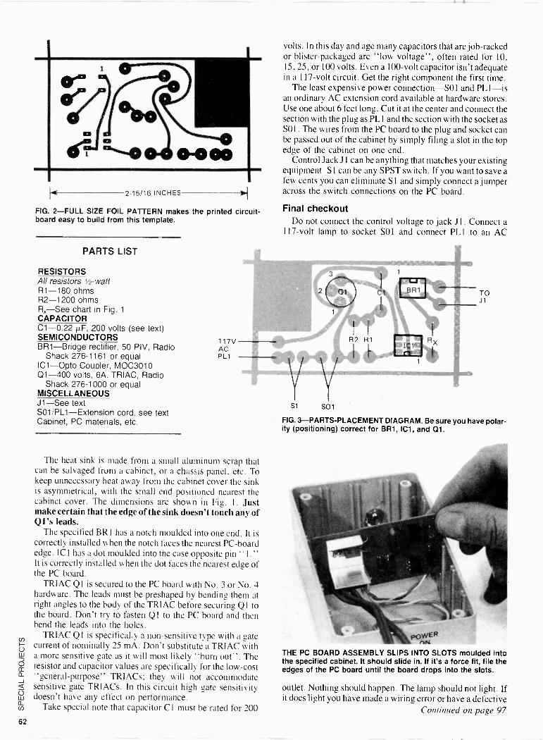
lc 2-15/16 INCHES
FIG. 2-FULL SIZE FOIL PATTERN makes the printed circuit - board easy to build from this template.
PARTS LIST
RESISTORS All resistors 1/2 -watt R1-180 ohms R2-1200 ohms Fix-See chart in Fig. 1
CAPACITOR C1-0.22 µF, 200 volts (see text) SEMICONDUCTORS BR1-Bridge rectifier, 50 PIV, Radio
Shack 276-1161 or equal IC1-Opto Coupler, MOC3010 01-400 volts, 6A. TRIAC, Radio
Shack 276-1000 or equal MISCELLANEOUS J1-See text S01/PL1-Extension cord, see text Cabinet, PC materials, etc.
117V AC PL1
The heat sink is made from a small aluminum scrap that can be salvaged from a cabinet, or a chassis panel, etc. To keep unnecessary heat away from the cabinet cover the sink is asymmetrical, with the small end positioned nearest the cabinet cover. The dimensions are shown in Fig. 1. Just make certain that the edge of the sink doesn't touch any of Ql's leads.
The specified BR I has a notch moulded into one end. It is correctly installed when the notch faces the nearest PC -board edge. ICI has a dot moulded into the case opposite pin " I . " It is correctly installed when the dot faces the nearest edge of the PC board.
TRIAC Q1 is secured to the PC board with No. 3 or No. 4 hardware. The leads must be preshaped by bending them at right angles to the body of the TRIAC before securing Q I to the board. Don't try to fasten QI to the PC board and then bend the leads into the holes.
TRIAC Q1 is specifically a non -sensitive type with a gate current of nominally 25 mA. Don't substitute a TRIAC with a more sensitive gate as it will most likely "burn out". The resistor and capacitor values are specifically for the low-cost "general-purpose" TRIACs; they will not accommodate sensitive -gate TRIACs. In this circuit high gate sensitivity doesn't have any effect on performance.
Take special note that capacitor Cl must be rated for 200
volts. In this day and age many capacitors that are job -racked or blister -packaged are "low voltage", often rated for 10, 15, 25, or 100 volts. Even a 100 -volt capacitor isn't adequate in a 117 -volt circuit. Get the right component the first time.
The least expensive power connection-SO 1 and PLI-is an ordinary AC extension cord available at hardware stores. Use one about 6 feet long. Cut it at the center and connect the section with the plug as PL 1 and the section with the socket as SO1. The wires from the PC board to the plug and socket can be passed out of the cabinet by simply filing a slot in the top edge of the cabinet on one end.
Control Jack J1 can be anything that matches your existing equipment. S 1 can be any SPST switch. If you want to save a few cents you can eliminate S 1 and simply connect a jumper across the switch connections on the PC board.
Final checkout Do not connect the control voltage to jack J1. Connect a
117 -volt lamp to socket SO 1 and connect PL 1 to an AC
TO J1
sol FIG. 3-PARTS-PLACEMENT DIAGRAM. Be sure you have polar- ity (positioning) correct for BR1, IC1, and Qi.
THE PC BOARD ASSEMBLY SLIPS INTO SLOTS moulded into the specified cabinet. It should slide in. If it's a force fit, file the edges of the PC board until the board drops into the slots.
outlet. Nothing should happen. The lamp should not light. If it does light you have made a wiring error or have a defective
Continued on page 97
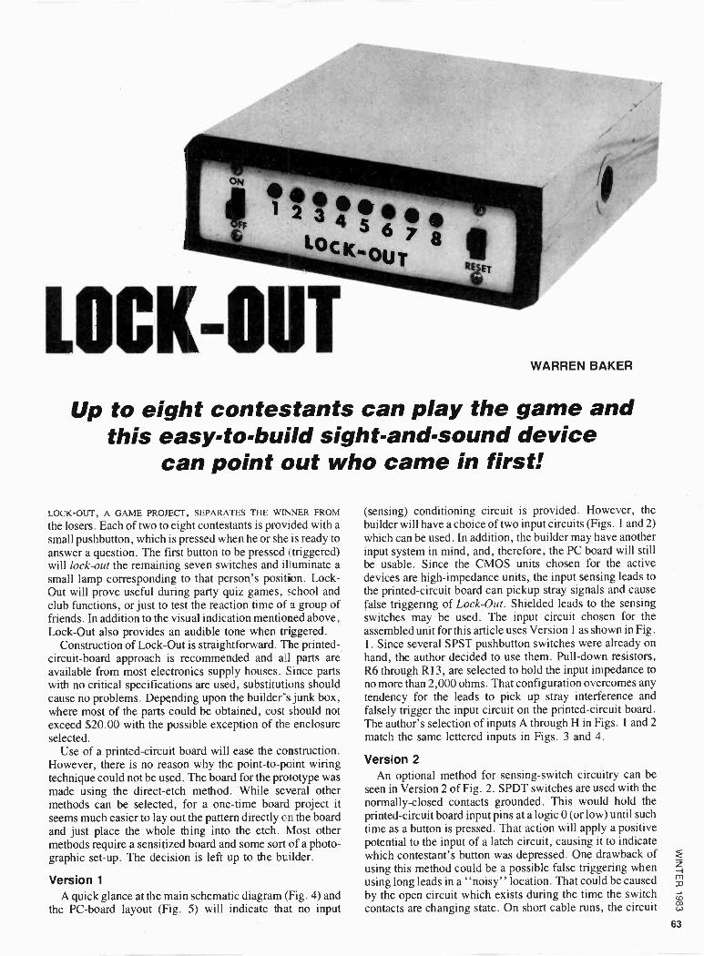
LOCK-OUT WARREN BAKER
Up to eight contestants can play the game and this easy -to -build sight -and -sound device
can point out who came in first!
LOCK-OUT, A GAME PROJECT, SEPARATES THE WINNER FROM
the losers. Each of two to eight contestants is provided with a
small pushbutton, which is pressed when he or she is ready to answer a question. The first button to be pressed (triggered) will lock-out the remaining seven switches and illuminate a small lamp corresponding to that person's position. Lock - Out will prove useful during party quiz games, school and club functions, or just to test the reaction time of a group of friends. In addition to the visual indication mentioned above, Lock -Out also provides an audible tone when triggered.
Construction of Lock -Out is straightforward. The printed - circuit -board approach is recommended and all parts are available from most electronics supply houses. Since parts with no critical specifications are used, substitutions should cause no problems. Depending upon the builder's junk box, where most of the parts could be obtained, cost should not exceed $20.00 with the possible exception of the enclosure selected.
Use of a printed -circuit board will ease the construction. However, there is no reason why the point-to-point wiring technique could not be used. The board for the prototype was made using the direct -etch method. While several other methods can be selected, for a one-time board project it
seems much easier to lay out the pattern directly on the board and just place the whole thing into the etch. Most other methods require a sensitized board and some sort of a photo- graphic set-up. The decision is left up to the builder.
Version 1
A quick glance at the main schematic diagram (Fig. 4) and the PC -board layout (Fig. 5) will indicate that no input
(sensing) conditioning circuit is provided. However, the builder will have a choice of two input circuits (Figs. 1 and 2) which can be used. In addition, the builder may have another input system in mind, and, therefore, the PC board will still be usable. Since the CMOS units chosen for the active devices are high -impedance units, the input sensing leads to the printed -circuit board can pickup stray signals and cause false triggering of Lock -Out. Shielded leads to the sensing switches may be used. The input circuit chosen for the assembled unit for this article uses Version 1 as shown in Fig. 1. Since several SPST pushbutton switches were already on hand, the author decided to use them. Pull -down resistors, R6 through R13, are selected to hold the input impedance to no more than 2,000 ohms. That configuration overcomes any tendency for the leads to pick up stray interference and falsely trigger the input circuit on the printed -circuit board. The author's selection of inputs A through H in Figs. 1 and 2
match the same lettered inputs in Figs. 3 and 4.
Version 2
An optional method for sensing -switch circuitry can be seen in Version 2 of Fig. 2. SPDT switches are used with the normally -closed contacts grounded. This would hold the printed -circuit board input pins at a logic 0 (or low) until such time as a button is pressed. That action will apply a positive potential to the input of a latch circuit, causing it to indicate which contestant's button was depressed. One drawback of using this method could be a possible false triggering when using long leads in a "noisy" location. That could be caused by the open circuit which exists during the time the switch contacts are changing state. On short cable runs, the circuit
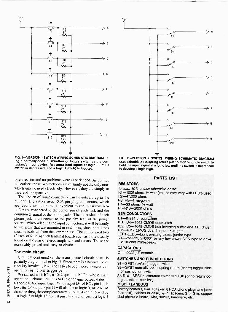
V C C
o S3
o S4
S5 o
R6 2K - R7
2K
R8
2K
-4VMr-
S6 R9
2K 11h
S7
S8
- o S9
o S10
o R10
o
2K
R11
2K ---MNt-
R12 2K
-Weir -- R13 2K,
> A
8
C
D
E
F
G
i H
FIG. 1-VERSION 1 SWITCH WIRING SCHEMATIC DIAGRAM us- ing a normally -open pushbutton or toggle switch as the con- testant's input device. Resistors hold inputs at logic 0 until a switch is depressed, and a logic 1 (high) is inputed.
operates fine and no problems were experienced. As pointed out earlier, those two methods are certainly not the only ones which may be used effectively. However, they are simply to wire and inexpensive.
The choice of input connectors can be entirely up to the builder. The author used RCA pin -plug connectors, which are readily available and convenient to use. Resistors R6 - R13 were connected to the center pin of each jack and the common terminal of the phono jacks. The outer shell of each phono jack is connected to the positive lead of the power source. When selecting the input connectors, it will be handy to use jacks that are mounted in multiples, since both leads must be isolated from the common use. The author used two (2) sets of four (4) each terminal boards such as those usually found on the rear of stereo amplifiers and tuners. Those are reasonably priced and easy to obtain.
The main circuit Circuitry contained on the main printed -circuit board is
partially diagrammed in Fig. 3. Since there is a duplication of circuitry involved, it will be easier to begin describing circuit operation using one trigger path.
We started with IC 1, a 4042 quad latch IC 1, whose main operational characteristic is to flip or change output states in response to the input logic. When input D4 of ICI , pin 14, is low, the Q4 output (pin 1) will also be at logic 0, or low. At the same time, the complementary output Q4 at pin 15 will be at a logic 1 or high. If input at pin 14 now changes to a logic 1
vCC
o o
S3 o o o
ce i°
o4/) S6
o o
oS7-
o
o" S8
o o o4`S9
> A
B
C
D
E
F
G
H
FIG. 2-VERSION 2 SWITCH WIRING SCHEMATIC DIAGRAM uses a double -pole, spring -return pushbutton or toggle switch to hold the input signal at a logic low until the switch is depressed to develop a logic high.
PARTS LIST RESISTORS 1/4 watt, 10% unless otherwise noted R1-1000 ohms, 1/2 -watt (values may vary with LED's used) R2-47,000 ohms R3, R5-1 megohm R4-33 ohms, 1/2 watt R6 -R13-2000 ohms
SEMICONDUCTORS D1-IN914 or equivalent IC1, IC4-4042 CMOS quad latch IC2, IC5-4049 CMOS hex inverting buffer and TTL driver IC3-4012 CMOS dual 4 -input NAND gate LED1-LED8-Light emitting diode, jumbo type Q1 -2N2222, 2N3601 or any low power NPN type to drive
2 -10 -ohm mini -speaker
CAPACITORS C1-.0022 µF ceramic
SWITCHES AND PUSHBUTTONS S1-SPST (oNIoFF) toggel switch S2-SPST normally -open, spring -return (RESET) toggel, slide
or pushbutton switch. S3-S10-SPST pushbutton switch or STDP spring -return tog-
gle switch-see text. MISCELLANEOUS Battery holder(s) 2 -in. speaker, 8 RCA phono plugs and jacks (see text), cabinet or case, 7/a -in. spacers, 3 x 3 in. copper clad phenolic board, wire, solder, hardware, etc.
64
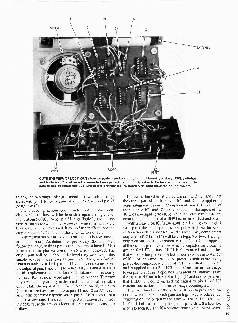
ICI Cl R5
BATTERIES
IC3
IC4
GUTS EYE VIEW OF LOCK-OUT showing parts layout on printed -circuit board, speaker, LEDS, switches and batteries. Circuit board is mounted on spacers permitting speaker to be located underneath. Be sure to use stranded hook-up wire to interconnect the PC board with parts mounted on the cabinet.
(high), the two output pins just mentioned will also change states with pin 1 following pin 14's input signal, and pin 15
going low (0). The preceding actions occur under certain other con-
ditions. One of those will be dependent upon the logic level found at pin 5 of ICI . When pin 5 is high (logic 1), the actions pointed out above will apply. However, when pin 5 is at logic 0, or low, the input levels will have no further affect upon the output states of IC 1. This is the latch action of IC 1.
Assume that pin 5 is at a logic 1 and a logic 1 is also present at pin 14 (input). As determined previously, the pin 1 will follow the input, making pin 1 output become a logic 1. Also assume that the plus voltage on pin 5 is now removed. The output pins will be latched at the level they were when this enable voltage was removed from pin 5. Also, any further action or activity at the input pin 14 will have no control over the output at pins 1 and 15. The 4042 unit (IC 1 and 1C4) used in this application contains four such latches as previously outlined. IC4's circuitry operates in a like manner. To prove to yourself that you fully understand the action of the latch circuit, take the input at H in Fig. 3 from a low (0) to a high (1) state to see how the outputs at pins 11 and 12 on IC4 react. Also consider what happens when pin 5 of IC4 goes from a high to a low state. The circuit in Fig. 3 was drawn as a mirror image because the action is identical, thus making it easier to follow.
Following the schematic diagram in Fig. 3 will show that the output pins of the latches in IC 1 and IC4 are applied to other integrated circuits. Complement pins Q4 and Q3 of each latch in IC 1 and IC4 are connected to the inputs of the 4012 dual 4 -input gate (IC3) while the other ouput pins are connected to the input of a 4049 hex inverter (IC2 and IC5).
With a logic 1 on ICI's D4 input, pin 1 will go to a logic 1
since pin 5, the enable pin, has been pulled high via the action of Vcc through resistor R5. At the same time, complement output pin of IC 1 (pin 15) will be at a logic 0 or low. The high output on pin 1 of IC 1 is applied to the IC2, pin 7, and appears at the output, pin 6, as a low which completes the circuit to ground for LED1; thus, LED1 is illuminated and signifies that someone has pressed the button corresponding to A input of IC 1. At the same time as the previous actions are taking place, the complement pin 15 of ICI has shifted to a logic 0 and is applied to pin 2 of IC3. As before, the mirror image lower portion of Fig. 3 operates in an identical manner. Trace the input at H from a low (0) to high (1) and see for yourself that LED8 will come on and the signal to pin 11 of IC3 matches the action of its mirror -image counterpart.
The main function of the gates in IC3 is to provide a low output when inputs to each gate are high. At any other input combination, the output of the gates will be in the high state. In Fig. 3, before a high input signal is provided, the four low inputs to both IC 1 and IC4 produce four high outputs to each
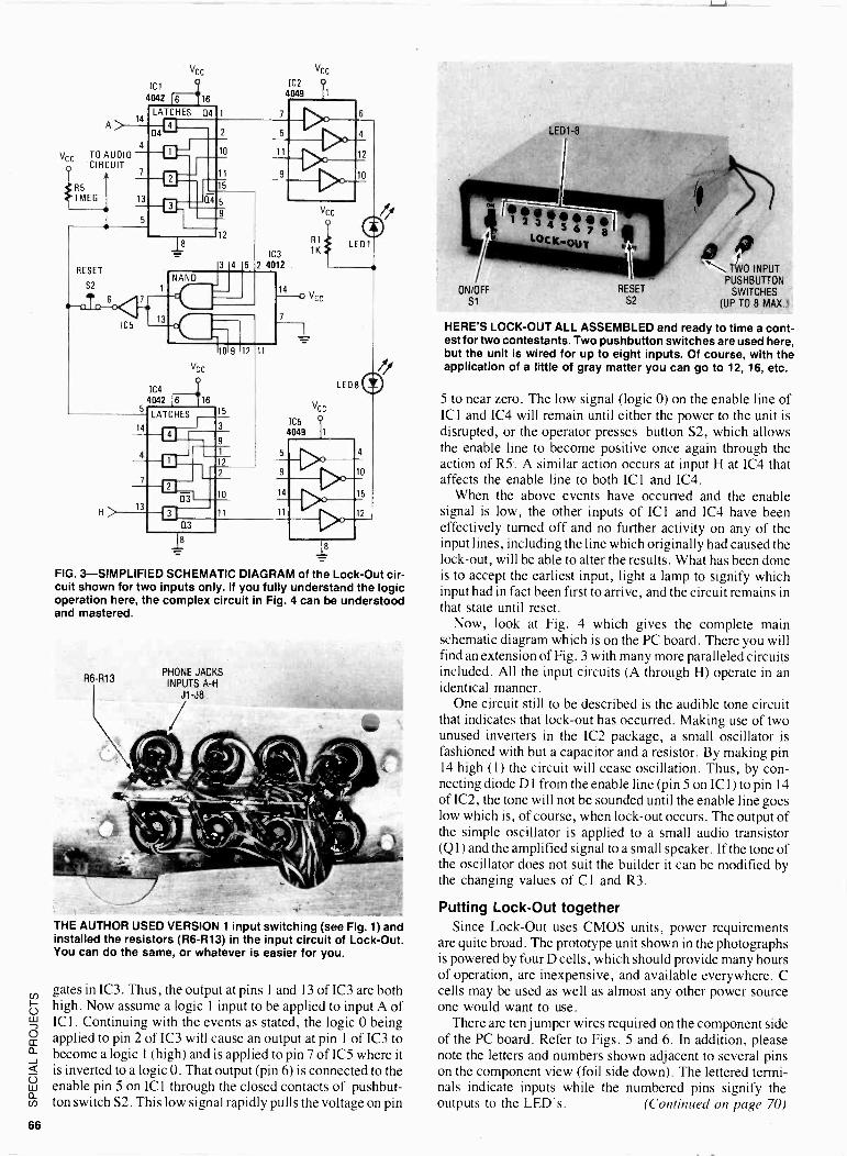
IC1
4042
VCC
f6 16
14 A> LATCHES 04 1
D4 2
vCqC
TO 4
10 AUDIO CIRCUIT
7 11
15 R5
1MEG 13 04
9
12
RESET 3 4 5 2
NAND S2
7 13 IC5
10 9 112 11
Vcc
IC4
4042 16 16
5 LATCHES 15
14 3 141
9
12
031 10
11 H 13 Q
03
1
VCC
1C2
4049
7
IC3
4012
14
7
VCC
R1
1K
VCC
VCC
IC5
4049
5 4
9 10
14 15
11 12
4
12
10
LED 1
LED8
rr
FIG. 3-SIMPLIFIED SCHEMATIC DIAGRAM of the Lock -Out cir- cuit shown for two inputs only. If you fully understand the logic operation here, the complex circuit in Fig. 4 can be understood and mastered.
R6 -R13 PHONE JACKS
INPUTS A -H
J1 -J8
THE AUTHOR USED VERSION 1 input switching (see Fig. 1) and installed the resistors (R6 -R13) in the input circuit of Lock -Out. You can do the same, or whatever is easier for you.
gates in IC3. Thus, the output at pins 1 and 13 of IC3 are both high. Now assume a logic 1 input to be applied to input A of ICI. Continuing with the events as stated, the logic 0 being applied to pin 2 of IC3 will cause an output at pin 1 of IC3 to become a logic 1 (high) and is applied to pin 7 of IC5 where it is inverted to a logic O. That output (pin 6) is connected to the enable pin 5 on IC1 through the closed contacts of pushbut- ton switch S2. This low signal rapidly pulls the voltage on pin
IEp1-8
DK-OUT 8
ON/OFF
S1
RESET
S2
TWO INPUT PUSHBUTTON
SWITCHES (UP TO 8 MAX.)
HERE'S LOCK-OUT ALL ASSEMBLED and ready to time a cont- est for two contestants. Two pushbutton switches are used here, but the unit is wired for up to eight inputs. Of course, with the application of a little of gray matter you can go to 12, 16, etc.
5 to near zero. The low signal (logic 0) on the enable line of IC1 and IC4 will remain until either the power to the unit is disrupted, or the operator presses button S2, which allows the enable line to become positive once again through the action of RS.. A similar action occurs at input H at IC4 that affects the enable line to both IC1 and IC4.
When the above events have occurred and the enable signal is low, the other inputs of IC1 and IC4 have been effectively turned off and no further activity on any of the input lines, including the line which originally had caused the lock-out, will be able to alter the results. What has been done is to accept the earliest input, light a lamp to signify which input had in fact been first to arrive, and the circuit remains in that state until reset.
Now, look at Fig. 4 which gives the complete main schematic diagram which is on the PC board. There you will find an extension of Fig. 3 with many more paralleled circuits included. All the input circuits (A through H) operate in an identical manner.
One circuit still to be described is the audible tone circuit that indicates that lock-out has occurred. Making use of two unused inverters in the IC2 package, a small oscillator is fashioned with but a capacitor and a resistor. By making pin 14 high (1) the circuit will cease oscillation. Thus, by con- necting diode D1 from the enable line (pin 5 on IC 1) to pin 14 of IC2, the tone will not be sounded until the enable line goes low which is, of course, when lock-out occurs. The output of the simple oscillator is applied to a small audio transistor (Q1) and the amplified signal to a small speaker. If the tone of the oscillator does not suit the builder it can be modified by the changing values of Cl and R3.
Putting Lock -Out together Since Lock -Out uses CMOS units, power requirements
are quite broad. The prototype unit shown in the photographs is powered by four D cells, which should provide many hours of operation, are inexpensive, and available everywhere. C cells may be used as well as almost any other power source one would want to use.
There are ten jumper wires required on the component side of the PC board. Refer to Figs. 5 and 6. In addition, please note the letters and numbers shown adjacent to several pins on the component view (foil side down). The lettered termi- nals indicate inputs while the numbered pins signify the outputs to the LED's. (Continued on page 70)
66
If you like to make things work... and then find out why they work-
you could b getting for doing something y
really Learn electronics...right on upto an enjoy. g Associate Degree...in your own home without giving up your present job or income.
People who really like their work get ahead faster. And, when your natural abilities match the job requirements, you have an
extra advantage. When you use
practical training to sharpen your skills, your odds are better for keeping your job even if others are losing theirs. So, if you find satisfaction and interest in making things work, a career in electronics may be for you.
WHY ELECTRONICS IN THE 80's Opportunity.
The field of electronics simply offers more career opportunities - and more job se-
curity - than most other fields today. Take digital technology, for example. Much of the new telecommunications, data processing, and production equipment depends upon sophisticated microprocessors to receive, sort, and send digital signals in micro- seconds. Two of CIE's newest home study courses combine digital electronics theory with actual experience on digital equipment. Successful completion of either one of those courses is creditable toward CIE's Associate Degree program. That's right...you can earn
an Associate Degree without attending a
single class session.
MAKING THINGS WORK Many of CIE's Career Courses stress "hands- on" training. We believe textbook knowl- edge is important - but it's just as important to know how to apply your book learning in practical situations. From basic circuitry in CIE's Personal Training Laboratory in several Career Courses, through the Microprocessor Training Laboratory in the Associate Degree program, CIE helps chan- nel your desire to "make things work" into skills you can sell.
IN A CLASS BY YOURSELF One of the great benefits of home study is
the independence it gives you. You study where and when you want to. You move as
fast as you can handle it. There's no class-
room to go to because with CIE, the classroom comes to you! But, you're never
alone. When you request help, the CIE electronics expert best qualified will personally respond in writing.
SET YOUR OWN GOALS CIE's wide selection of courses gives you many options. You start with a Career Course that suits your talents. Then, since
more than half of CIE's courses include a
series of optional lessons to prepare you to pass the government -administered FCC License exam, you can get an FCC License ...a requirement for some electronics jobs and a credential for a// electronics jobs. You may then go on and earn an Associate in Applied Science Degree in Electronics Engineering Technology. It's all up to you!
START MAKING THINGS WORK
FOR YOU Send today for the CIE school
catalog and complete package of career information. It's all FREE, and it will help you decide where you want to start and how far you want to go. For your convenience, we'll try to have a school representative con- tact you to review the various educational programs and assist in course selection. Just mail the postage -paid card or write, men- tioning the name and date of this magazine. We want to help you make things work, so
send for your FREE school catalog today!
CIE's Microprocessor Training Laboratory, an integral part of the Associate Degree program, lets the advanced student apply digital technology in many of the same ways electronics professionals do.
CIECleveland Institute of Electronics, Inc. 1776 East 17th Street, Cleveland, Ohio 44114
Accredited Member National Home Study Council
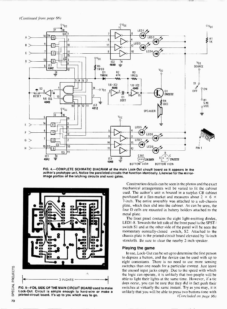
(Continued from page 66)
i
A >
B >
C >
D
14
IF
Vcc
16
04 04
13
5
S2 6
IC1 4042
2
0
LED 1 ff 5 4
LED2
11 12LED3
11
15
04 3
9
7
RESET 1/6-105 4049
5
12
3 4 5 2
13
8
Vice
R5
fr
9 > 10 LEDO
IC2 I8 4049 =
1MEG
01 R2 R3 1N914 47K 1MEG
1/6- 1C2
14 4049 oVCC 3
Vcc
16
E >
F ] G >
H >
14
13 03
10
15
3
9
9
03 l
12 11
1 1C3
4012
12
2
10
03 IC1
4042
11
.0022
VCC
LED5 4
9 2 LEDE
LEDI 14 1\_ 15
11 12 LEDE J!
IC5 18 4049 =
CBE 000 2N3601
E 2N2222
B
C
BOTTOM VIEW BOTTOM VIEW
FIG. 4.-COMPLETE SCHMATIC DIAGRAM of the main Lock -Out circuit board as it appears in the author's prototype unit. Notice the paralleled circuits that function identically. Likewise for the mirror - image portion of the latching circuits and NAND gates.
VCC
SOURCE
Si
OFF
3 INCHES
FIG. 5-FOIL SIDE OF THE MAIN CIRCUIT BOARD used to make Lock -Out. Circuit is simple enough to hard -wire or make a printed -circuit board. It's up to you which way to go.
° Vcc
e R1
1K
ON
B1 5-10
PIN 1
Construction details can be seen in the photos and the exact mechanical arrangements will be varied to fit the cabinet used. The author's unit is housed in a surplus CB cabinet purchased at a flea -market and measures about 2 x 6 x 7 -inch. The entire assembly was attached to a sub -chassis plate, which then slid into the cabinet. As can be seen, the four D cells are mounted in battery holders attached to the metal plate.
The front panel contains the eight light -emitting diodes, LED 1-8. Towards the left side of the front panel is the SPST / switch S1 and at the other side of the panel will be seen the momentary normally -closed switch, S2. Attached to the chassis plate is the printed -circuit board elevated by 7/s -inch standoffs. Be sure to clear the nearby 2 -inch speaker.
Playing the game In use, Lock -Out can be set up to determine the first person
to depress a button, and the device can be used with up to eight contestants. There is no need to use more sensing switches than one needs for a particular contest. Just leave the unused input jacks empty. Due to the speed with which the logic can operate, it is unlikely that two people will be able to light their lights at the same time. However, if a tie does occur, you can be sure that they did in fact push their switches at virtually the same instant. Try as you may, it is unlikely that you will be able to press two buttons (one with
(Concluded on page 96) 70
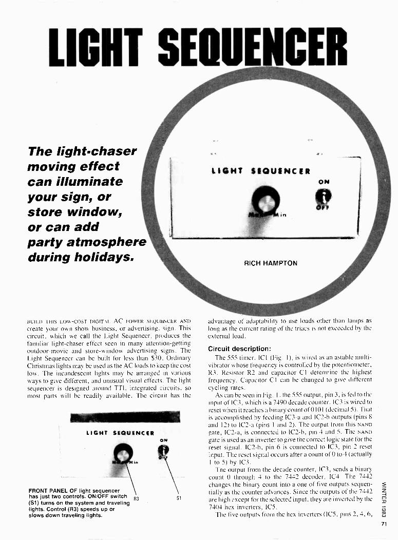
LICHT SEQUENCER
The light -chaser moving effect can illuminate your sign, or store window, or can add party atmosphere during holidays.
BUILD THIS LOW-COST DIGITAL AC POWER SEQUENCER AND
create your own show business, or advertising, sign. This circuit, which we call the Light Sequencer, produces the familiar light -chaser effect seen in many attention -getting outdoor -movie and store -window advertising signs. The Light Sequencer can be built for less than $30. Ordinary Christmas lights may be used as the AC loads to keep the cost low. The incandescent lights may be arranged in various ways to give different, and unusual visual effects. The light sequencer is designed around TTL integrated circuits, so most parts will be readily available. The circuit has the
iiii1,.111111111111111111111111
LIGHT SEQUENCER ON
FRONT PANEL OF light sequencer has just two controls. ON OFF switch
R3 (S1) turns on the system and traveling lights. Control (R3) speeds up or slows down traveling lights.
S1
advantage of adaptability to use loads other than lamps as
long as the current rating of the triacs is not exceeded by the external load.
Circuit description: The 555 timer, IC (Fig. 1). is wired as an astable multi -
vibrator whose frequency is controlled by the potentiometer, R3. Resistor R2 and capacitor C 1 determine the highest frequency. Capacitor C 1 can be changed to give different cycling rates.
As can be seen in Fig. 1, the 555 output, pin 3, is fed to the input of IC3, which is a 7490 decade counter. IC3 is wired to reset when it reaches a binary count of 0101 (decimal 5). That is accomplished by feeding IC3-a and IC2-b outputs (pins 8
and 12) to IC2-a (pins 1 and 2). The output from this NAND
gate, IC2-a, is connected to IC2-b, pin 4 and 5. The NAND
gate is used as an inverter to give the correct logic state for the reset signal. IC2-b, pin 6 is connected to IC3, pin 2 reset input. The reset signal occurs after a count of 0 to 4 (actually 1 to 5) by IC3.
The output from the decade counter, IC3, sends a binary count 0 through 4 to the 7442 decoder, 1C4. The 7442 changes the binary count into a one of five outputs sequen- tially as the counter advances. Since the outputs of the 7442 are high except for the selected input, they are inverted by the 7404 hex inverters, IC5.
The five outputs from the hex inverters (IC5, pins 2, 4, 6,
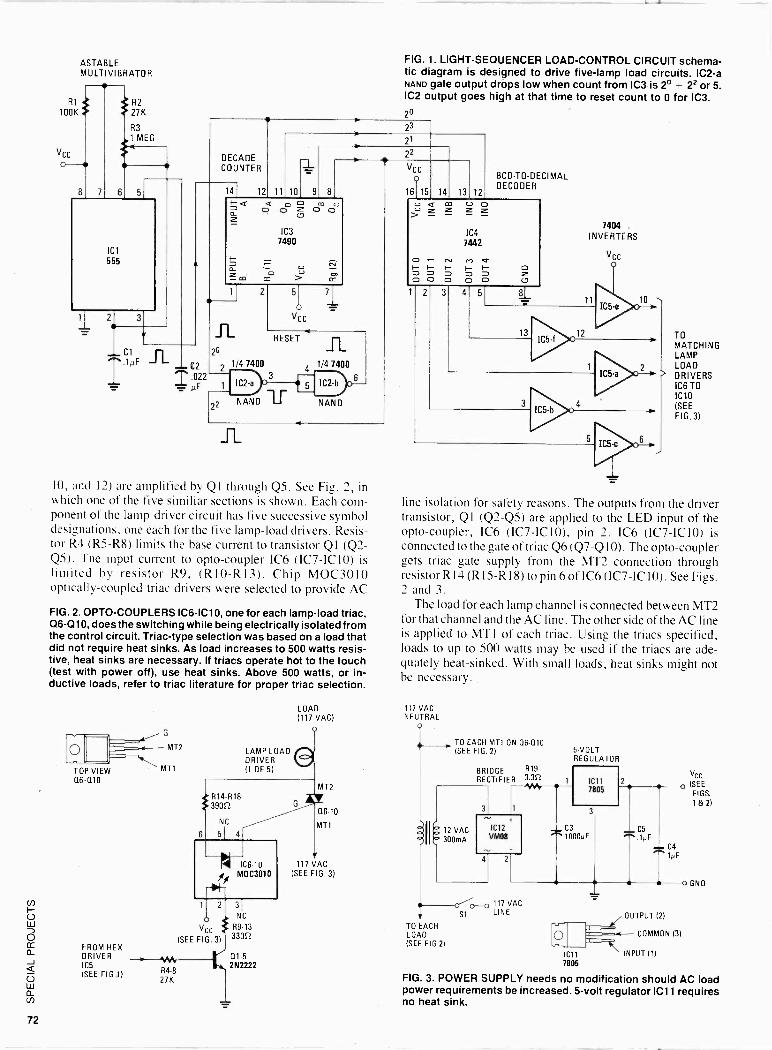
R1
100K
ASTABLE MU LTI VIB R ATO R
eR2 27K
R3
*1. MEG
6 5
IC1
555
FIG. 1. LIGHT -SEQUENCER LOAD -CONTROL CIRCUIT schema- tic diagram is designed to drive five -lamp load circuits. IC2-a NAND gate output drops low when count from IC3 is 2° - 22 or 5. IC2 output goes high at that time to reset count to 0 for IC3.
20
DECADE COUNTER
14 12 11
23
21
10 9 8
Q Z
0
o cc
p O m c+ Z a O O
IC3 7490
C2
1.022 µF 1
22 NANO
2
20
2 1/4 7400
VCC
RESET
3 4
1/4 744000
IC2-b )D
NAND
10, and 12) are amplified by QI through Q5. See Fig. 2, in which one of the five similiar sections is shown. Each com- ponent of the lamp -driver circuit has five successive symbol designations. one each for the five lamp -load drivers. Resis- tor R4 (R5 -R8) limits the base current to transistor Q l (Q2 - Q5). The input current to opto -coupler IC6 (1C7-IC10) is limited by resistor R9, (R10 -R13). Chip MOC3010 optically -coupled triac drivers were selected to provide AC
FIG. 2. OPTO -COUPLERS IC6-1C1 0, one for each lamp -load triac, 06-010, does the switching while being electrically isolated from the control circuit. Triac-type selection was based on a load that did not require heat sinks. As load increases to 500 watts resis- tive, heat sinks are necessary. If triacs operate hot to the touch (test with power off), use heat sinks. Above 500 watts, or in- ductive loads, refer to triac literature for proper triac selection.
TOP VIEW Q6-010
FROM HEX DRIVER 105
(SEE FIG.1)
I
R14 R18 3902
LAMP LOAD DRIVER (1 OF 5)
NC
51 4
IC6-10 MOC3010
2
o Vcc
(SEE FIG. 3)
R4-8
27K
3¡ NC
R9-13 33012
01-5 2N2222
LOAD (117 VAC)
MT2
Q6-10
MT1
117 VAC (SEE FIG. 3)
22
VCC o
16
BCD -TO -DECIMAL
15 14 13 12 DECODER
Q m U O Z Z Z Z
I-
O 2
N I-
O 3
1C4
7442
PI
O 4
F O
5
3 IC5-I
7404 INVERTERS
VCC
12
IC5-h
IC5-a
IC5-c
TO MATCHING LAMP LOAD DRIVERS IC6 TO ICIO (SEE FIG. 3)
line isolation for safety reasons. The outputs from the driver transistor, QI (Q2 -Q5) are applied to the LED input of the opto -coupler, IC6 (IC7-1C10), pin 2. 106 (1C7 -1C10) is connected to the gate of triac Q6 (Q7 -Q10). The opto -coupler gets triac gate supply from the MT2 connection through resistor R14 (R15 -R18) to pin 6 of IC6 (1C7-IC 10). See Figs. 2 and 3.
The load for each lamp channel is connected between MT2 for that channel and the AC line. The other side of the AC line is applied to MT1 of each triac. Using the triacs specified, loads to up to 500 watts may be used if the triacs are ade- quately heat-sinked. With small loads, heat sinks might not be necessary.
117 VAC NEUTRAL
TO EACH LOAD (SEE FIG 2)
TO EACH MT1 ON Q6-010 (SEE FIG. 2)
Si
BR DGE R19 RECTIFIER 3.312
0__0 117 VAC LINE
5 -VOLT REGULATOR
IC11 7805
FIG. 3. POWER SUPPLY needs no modification should AC load power requirements be increased. 5 -volt regulator IC1 1 requires no heat sink.
C4 1NF
Va.
(SEE FIGS.
1&21
GND
OUTPUT (21
COMMON (31
INPUT (1)
72
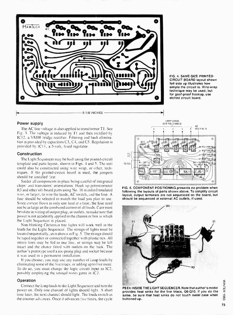
51 8 INCHES
Power supply 1 he AC line voltage is also applied to transformer T1. See
Fig. 3. The voltage is reduced by T1 and then rectified by IC12, a VM08 bridge rectifier. Filtering and hash elimina- tion is provided by capacitors C3, C4, and C5. Regulation is provided by IC 11, a 5 -volt, fixed regulator.
Construction The Light Sequencer may be built using the printed -circuit
template and parts layout, shown in Figs. 4 and 5. The unit could also be constructed using wire wrap, or other, tech- niques. If the printed -circuit board is used, the jumpers should be installed first.
Solder all components in place being careful of integrated chips' and transistors' orientations. Hook up potentiometer R3 and other off -board parts using No. 16 standard insulated wire, or larger, to wire the loads, AC switch, and the fuse. A fuse should be selected to match the load you plan to use. Since current flows in only one load at a time, the fuse need not be as large as the combined current of all loads. Care must be taken in wiring of output plug, or outlets, to make sure that power is not accidently applied to the chassis or box in which the Light Sequencer is placed.
Non -blinking Christmas tree lights will work well as the loads for the Light Sequencer. The strings of lights must be located sequentially, as is shown in Fig. 5. The strings should be taped together or connected together with plastic ties. All return lines may be fed to one line, or strings may be left intact and the chaser fitted with outlets on the back. The author's prototype used a six -prong plug and socket because it was used in a permanent installation.
If you choose, you may use any number of lamp loads by eliminating some of the five triacs, or adding up to five more. To do so, you must change the logic circuit input to IC2, possibly employing the unused NAND gates in IC2.
Operation Connect the lamp loads to the Light Sequencer and turn the
power on. Only one channel of lights should light. A short time later, the next channel should light. The loads switch as the counter advances. Once it advances five times, the cycle
To
TO R3
FIG. 4. SAME -SIZE PRINTED - CIRCUIT BOARD layout shown foil side up illustrates how simple the circuit is. Wire -wrap technique may be used: but for goof -proof hookup, use etched circuit board.
LAMP LOADS
(SEE FIG. 2 AND 3) A
3 1 2 5 4
w IC 14k
- R2- -R1-
\ Rifil_ R1
`R13-u2a5 `r - R12- G4
AC
(SEE FIG. 21
R19 , ,,,,rR11- (722 p3
FIG. 5. COMPONENT POSITIONING presents no problem when following the layouts of parts shown above. To simplify circuit layout, output terminals are not sequenced on the board, but should be sequenced at external AC outlets, if used.
PEEK INSIDE THE LIGHT SEQUENCER. Note that author's model provides heat sinks for the five triacs, Q6 -Q10. If you do the same, be sure that heat sinks do not touch metal case when buttoned -up.
73
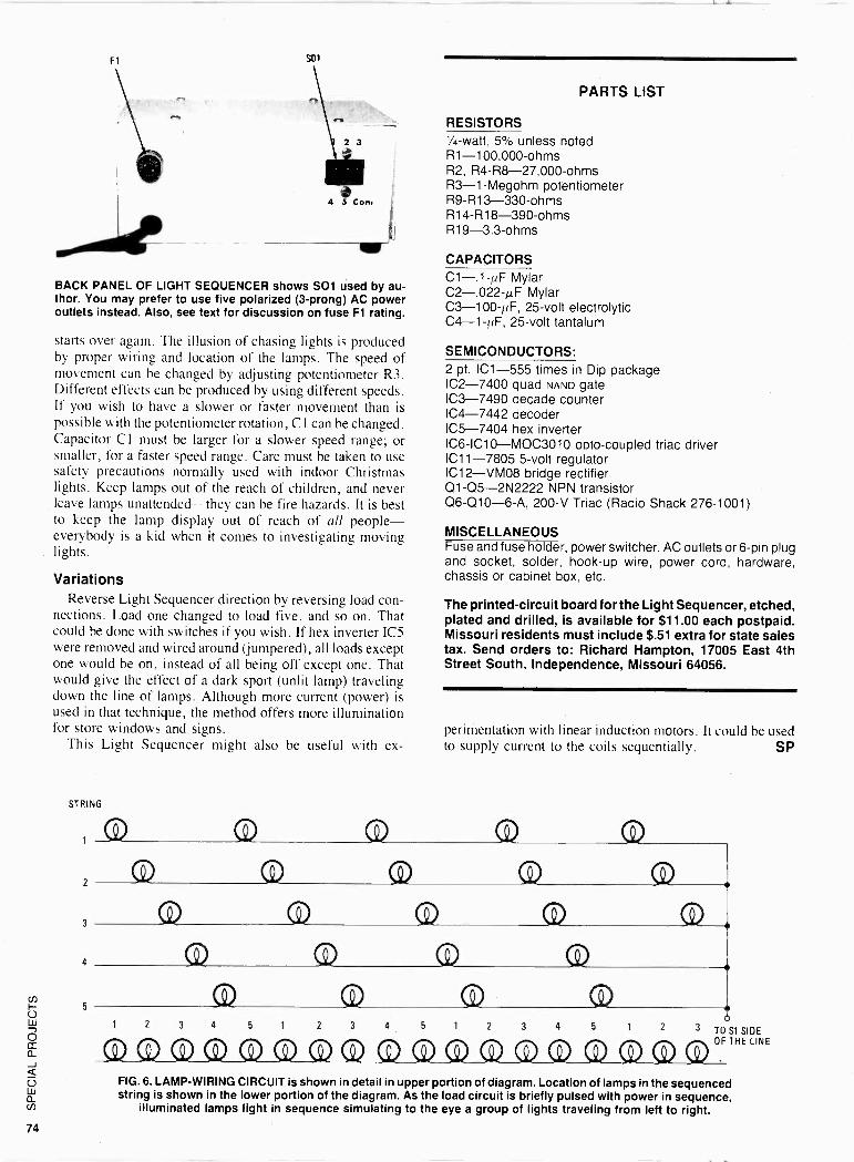
F1 soi
eft
BACK PANEL OF LIGHT SEQUENCER shows SO1 used by au- thor. You may prefer to use five polarized (3 -prong) AC power outlets instead. Also, see text for discussion on fuse F1 rating.
starts over again. The illusion of chasing lights is produced by proper wiring and location of the lamps. The speed of movement can be changed by adjusting potentiometer R3. Different effects can be produced by using different speeds. If you wish to have a slower or faster movement than is possible with the potentiometer rotation, C I can be changed. Capacitor Cl must be larger for a slower speed range; or smaller, for a faster speed range. Care must be taken to use safety precautions normally used with indoor Christmas lights. Keep lamps out of the reach of children, and never leave lamps unattended they can be fire hazards. It is best to keep the lamp display out of reach of all people- everybody is a kid when it comes to investigating moving lights.
Variations Reverse Light Sequencer direction by reversing load con-
nections. Load one changed to load five, and so on. That could be done with switches if you wish. If hex inverter IC5 were removed and wired around (jumpered), all loads except one would be on. instead of all being off except one. That would give the effect of a dark sport (unlit lamp) traveling down the line of lamps. Although more current (power) is used in that technique, the method offers more illumination for store windows and signs.
This Light Sequencer might also be useful with ex -
STRING
1
2
3
4
5
PARTS LIST
RESISTORS 1/4 -watt, 5% unless noted R1 -100,000 -ohms R2, R4 -R8 -27,000 -ohms R3-1-Megohm potentiometer R9 -R13 -330 -ohms R14 -R18 -390 -ohms R19 -3.3 -ohms
CAPACITORS C1-.1-i,F Mylar C2-.022 -µF Mylar C3 -100-14F. 25 -volt electrolytic 04-1-pF, 25 -volt tantalum
SEMICONDUCTORS: 2 pt. IC1-555 times in Dip package IC2-7400 quad NAND gate IC3-7490 decade counter IC4-7442 decoder 105-7404 hex inverter IC6-1C10-MOC3010 opto -coupled triac driver 1011-7805 5 -volt regulator IC12-VM08 bridge rectifier 01-05-2N2222 NPN transistor Q6 -Q10 -6-A, 200-V Triac (Radio Shack 276-1001)
MISCELLANEOUS Fuse and fuse holder, power switcher, AC outlets or 6 -pin plug and socket, solder, hook-up wire, power cord, hardware, chassis or cabinet box, etc.
The printed -circuit board for the Light Sequencer, etched, plated and drilled, is available for $11.00 each postpaid. Missouri residents must include $.51 extra for state sales tax. Send orders to: Richard Hampton, 17005 East 4th Street South, Independence, Missouri 64056.
perimentation with linear induction motors. It could be used to supply current to the coils sequentially. SP
Cº @ Q G G
G G
o 1 2 3 4 5 1 2 3 4 5 1 2 3 4 5 1 2 3 TO S1 SIDE
OF THE LINE
FIG. 6. LAMP -WIRING CIRCUIT is shown in detail in upper portion of diagram. Location of lamps in the sequenced string is shown in the lower portion of the diagram. As the load circuit is briefly pulsed with power in sequence,
illuminated lamps light in sequence simulating to the eye a group of lights traveling from left to right.

WARREN BAKER
DUAL
VOLTAGE
POWER
SUPPLY Budget dual -regulated power supply
with common ground adds test -bench punch for project builders
A VARIABLE -VOLTAGE POWER SUPPLY FOR THE ELECTRONICS
test or project bench can become a very worthwhile project for the electronics experimenter, ham radio operator, amateur or pro repairman, or hobbyist. The project presented here not only offers simplicity and low cost to assemble, but also contains two identical adjustable power supplies on the same small circuit board with each supply regulated in- dependently, but sharing a common ground.
A quick glance at the schematic diagram of the Dual Variable Power Supply (Fig. 1) will reveal the above - mentioned simplicity and at the same time point out that the dual heart of the power supply is really two regulator inte- grated circuits, IC1 and IC2. The diagram also makes it apparent that the two supplies differ only in their polarities with the upper one in the schematic diagram providing a positive output while the lower one is negative in respect to the common ground connection shown. Each supply can be operated independently of the other for general use where no common connections exist between the units under test. However, one important use for the power supply will be during experimenting with operational amplifiers (op -amps), which oftentimes require a so-called "split" power source with the positive and negative terminals both being isolated from the common ground of the op -amp. In this case, the Dual Variable Power Supply is a natural.
Although no enclosure or case is shown, the Dual Variable Power Supply may be mounted in any convenient cabinet that the builder may have available. Or, if desired, it can even be installed into the bench where most of the uses will be found. The power supply's small size, 31/2 -in. wide by 5'/46 - in. deep by 2 -in. high makes it easy to add the unit into existing test equipment if desired. Otherwise, the power
supply may be operated without a case without too much danger involved provided its base is insulated in the event it is placed on metal objects.
The two independently -adjustable regulated power suppl- ies may be set to any voltage within the range of approx- imately 1.25 VDC and 15 VDC with each supply capable of delivering up to 750 mA of current to the load. The exact limit will depend upon the individual voltage settings at the time. Further, each supply is protected against thermal over- loads by circuitry built into the IC regulators. All parts are common items and should be easily obtained from good electronics parts houses. In addition, parts, including the PC board (see Fig. 2), are available at the location listed in the Parts List. There is also a complete kit of parts available for those who prefer to go that route.
Putting it together Quite naturally, construction time will vary according to
many factors including the individual's own abilities. However, assuming that the builder has already rounded up all the required parts and has a pre -drilled and etched PC board on hand, there can be little reason to anticipate spend- ing more than one evening building the Dual Variable Power Supply. Using point-to-point wiring may take slightly lon- ger, since the parts must be attached to a chassis or perfboard.
If you are using the printed -circuit board approach, the recommended procedure for assembly will begin by install- ing four diodes, D1 through D4, in the positions shown on the parts layout in Fig. 3. Use caution to be certain that their polarities are as indicated by the color band on each unit. The diodes should be mounted about '/8 -inch above the board surface. Following the soldering and trimming of excess lead
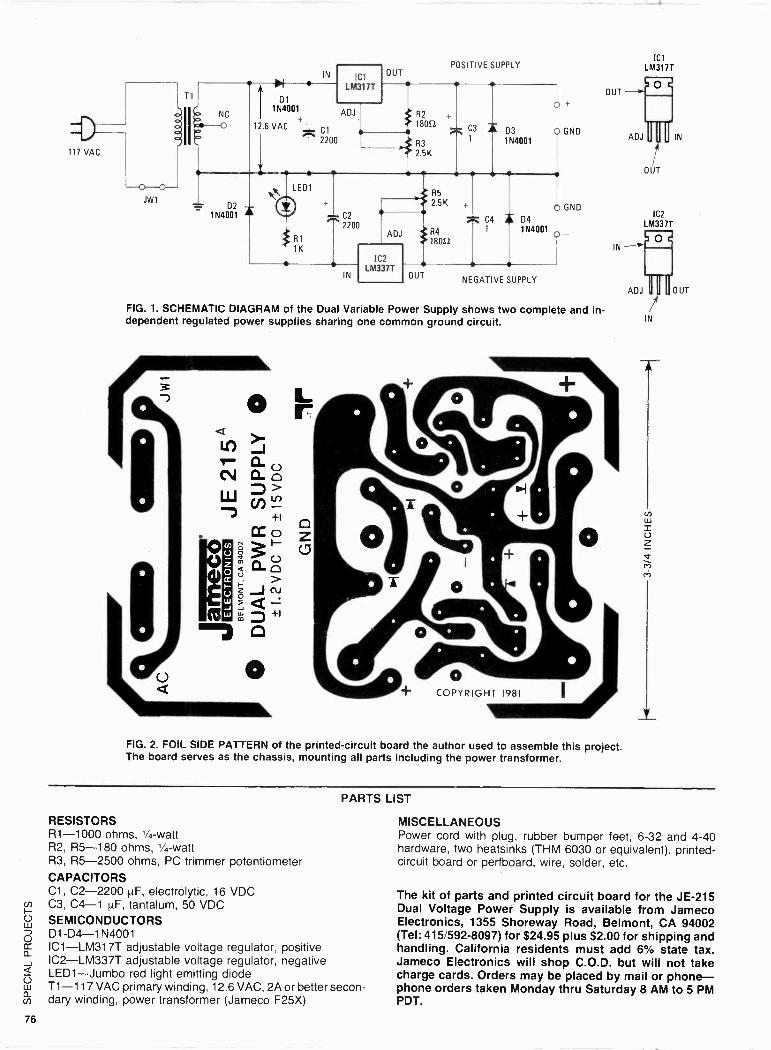
POSITIVE SUPPLY ICI
117 VAC
T1
JW1
IN
NC
o IC*
D1
1N4001
12.6 VAC
ICI LM317T
OUT
ADJ
* C1
2200
R2 +
18052
R3 2.5K
T C3 * 03 1 1N4001
O GND
02 1N4001
LED1
R1
1K
*C2 2200
ADJ
IN
IC2 LM337T
R5
2.5K
R4 18012
í* C4 * 04 1 1N4001
O GND
OUT NEGATIVE SUPPLY
FIG. 1. SCHEMATIC DIAGRAM of the Dual Variable Power Supply shows two complete and dependent regulated power supplies sharing one common ground circuit.
o r
o Z c
o
OUT
LM317T
OUT
IC2 LM337T
IN
O IN ---1"
ADJ 0 il U OUT
in- /
IN
o COPYRIGHT 1981
FIG. 2. FOIL SIDE PATTERN of the printed -circuit board the author used to assemble this project. The board serves as the chassis, mounting all parts including the power transformer.
PARTS LIST
RESISTORS R1-1000 ohms, 1/4 -watt R2, R5--180 ohms, 1/4 -watt R3, R5-2500 ohms, PC trimmer potentiometer CAPACITORS C1, C2-2200 µF, electrolytic, 16 VDC C3, C4-1 µF, tantalum, 50 VDC SEMICONDUCTORS Dl -D4 -1N4001 IC1-LM317T adjustable voltage regulator, positive IC2-LM337T adjustable voltage regulator, negative LED1-Jumbo red light emitting diode T1-117 VAC primary winding, 12.6 VAC, 2A or better secon- dary winding, power transformer (Jameco F25X)
MISCELLANEOUS Power cord with plug, rubber bumper feet, 6-32 and 4-40 hardware, two heatsinks (THM 6030 or equivalent), printed - circuit board or perfboard, wire, solder, etc.
The kit of parts and printed circuit board for the JE -215 Dual Voltage Power Supply is available from Jameco Electronics, 1355 Shoreway Road, Belmont, CA 94002 (Tel: 415/592-8097) for $24.95 plus $2.00 for shipping and handling. California residents must add 6% state tax. Jameco Electronics will shop C.O.D. but will not take charge cards. Orders may be placed by mail or phone- phone orders taken Monday thru Saturday 8 AM to 5 PM PDT.
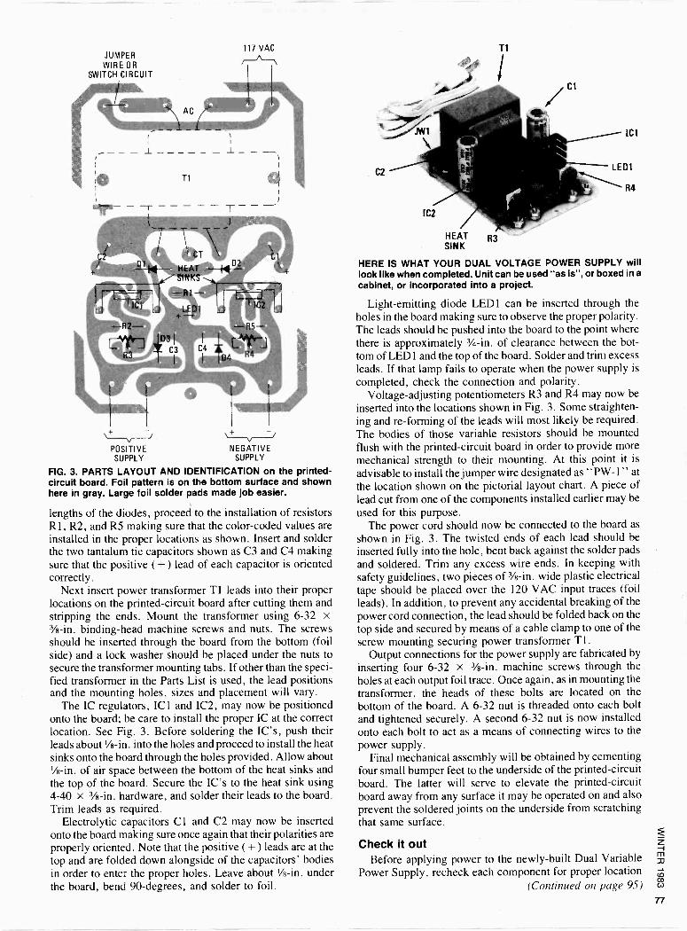
JUMPER WIRE OR
SWITCH CIRCUIT
AC
T1
POSITIVE NEGATIVE SUPPLY SUPPLY
FIG. 3. PARTS LAYOUT AND IDENTIFICATION on the printed - circuit board. Foil pattern is on the bottom surface and shown here In gray. Large foil solder pads made job easier.
lengths of the diodes, proceed to the installation of resistors R1, R2, and R5 making sure that the color -coded values are installed in the proper locations as shown. Insert and solder the two tantalum tie capacitors shown as C3 and C4 making sure that the positive (+) lead of each capacitor is oriented correctly.
Next insert power transformer Ti leads into their proper locations on the printed -circuit board after cutting them and stripping the ends. Mount the transformer using 6-32 x 3/8 -in. binding -head machine screws and nuts. The screws should be inserted through the board from the bottom (foil side) and a lock washer should be placed under the nuts to secure the transformer mounting tabs. If other than the speci- fied transformer in the Parts List is used, the lead positions and the mounting holes, sizes and placement will vary.
The IC regulators, IC1 and IC2, may now be positioned onto the board; be care to install the proper IC at the correct location. See Fig. 3. Before soldering the IC's, push their leads about Vs -in. into the holes and proceed to install the heat sinks onto the board through the holes provided. Allow about '/s -in. of air space between the bottom of the heat sinks and the top of the board. Secure the IC's to the heat sink using 4-40 x 3/8 -in. hardware, and solder their leads to the board. Trim leads as required.
Electrolytic capacitors C 1 and C2 may now be inserted onto the board making sure once again that their polarities are properly oriented. Note that the positive (+) leads are at the top and are folded down alongside of the capacitors' bodies in order to enter the proper holes. Leave about '/s -in. under the board, bend 90 -degrees, and solder to foil.
1C2
HEAT R3 SINK
HERE IS WHAT YOUR DUAL VOLTAGE POWER SUPPLY will look like when completed. Unit can be used "as is", or boxed In a
cabinet, or incorporated into a project.
Light -emitting diode LED1 can be inserted through the holes in the board making sure to observe the proper polarity. The leads should be pushed into the board to the point where there is approximately 3/4 -in. of clearance between the bot- tom of LED 1 and the top of the board. Solder and trim excess leads. If that lamp fails to operate when the power supply is
completed, check the connection and polarity. Voltage -adjusting potentiometers R3 and R4 may now be
inserted into the locations shown in Fig. 3. Some straighten- ing and re-forming of the leads will most likely be required. The bodies of those variable resistors should be mounted flush with the printed -circuit board in order to provide more mechanical strength to their mounting. At this point it is
advisable to install the jumper wire designated as "PW-1" at
the location shown on the pictorial layout chart. A piece of lead cut from one of the components installed earlier may be used for this purpose.
The power cord should now be connected to the board as shown in Fig. 3. The twisted ends of each lead should be inserted fully into the hole, bent back against the solder pads and soldered. Trim any excess wire ends. In keeping with safety guidelines, two pieces of 3/8 -in. wide plastic electrical tape should be placed over the 120 VAC input traces (foil leads). In addition, to prevent any accidental breaking of the power cord connection, the lead should be folded back on the top side and secured by means of a cable clamp to one of the screw mounting securing power transformer T1.
Output connections for the power supply are fabricated by inserting four 6-32 x 3/8 -in. machine screws through the holes at each output foil trace. Once again, as in mounting the transformer, the heads of these bolts are located on the bottom of the board. A 6-32 nut is threaded onto each bolt and tightened securely. A second 6-32 nut is now installed onto each bolt to act as a means of connecting wires to the power supply.
Final mechanical assembly will be obtained by cementing four small bumper feet to the underside of the printed -circuit board. The latter will serve to elevate the printed -circuit board away from any surface it may be operated on and also prevent the soldered joints on the underside from scratching that same surface.
ii
Check it out Before applying power to the newly -built Dual Variable
Power Supply, recheck each component for proper location (Continued on page 95)
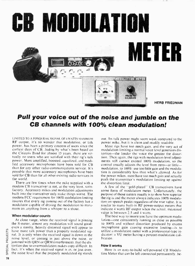
CB MODULATION
METER
HERB FRIEDMAN
Pull your voice out of the noise and jumble on the CB channels with 100% clean modulation!
LIMITED TO A PIPSQUEAK SIGNAL OF 4 -WATTS MAXIMUM RF output, it's no wonder that modulation, or talk power, has been a primary concern of users since the earliest days of CB. Juding by what's been heard on the Citizens Band for almost 15 years, there are vir- tually no users who are satisfied with their rig's talk power. More amplified, boosted, equalized, and modi- fied accessory microphones have been sold for CB than for any other radio -communications service. It's possible that more accessory microphones have been sold for CB than for all other existing radio services in the world.
There are few times when the mike supplied with a modern CB transceiver is not, at the very least, satis- factory. Accessory mikes and modulation adjustments built into the transceiver only make things worse. The modern FCC requirement for 100% modulation -limiting insures that every rig coming out of the factory has a modulator capable of driving the modulation to maxi- mum on anything from a whisper to a shout.
When modulator counts At close range, when the received signal is pinning
the S -meter, almost any modulation will sound good; even a mushy, heavily distorted signal will appear to have more talk power than a properly modulated sig- nal. It is only when the received signal is down in the noise level, or coming in just above the noise, or jammed with QRN or QRM (interference), that the dis- tortion due to overmodulation makes copy difficult. In fact, it's when the received signal is in, or just over, the noise level that the properly modulated rig stands
out. Its talk power might seem weak compared to the power mike, but it is clean and readily readable.
Most rigs have too much gain, and the very act of modulation -limiting a normal voice level generates dis- tortion-the louder the voice the greater the distor- tion. Then again, the rigs with modulation -level adjust- ments still cannot exceed 100% modulation, so the control usually adjusts the level from zero-or little- modulation, to 100%: use too little gain and the modula- tion is considerably less than what's allowed. As for the power mikes, most have too much gain and actually push the transmitter's modulation limiting up against the distortion limit.
A few of the "gold-plated" CB transceivers have some form of modulation meter. Unfortunately, the purpose of those meters usually is to show how superior the rig is and the meter always indicates 100% modula- tion on speech peaks regardless of the true value. It is similar to many built-in RF power -output meters that indicate 4 watts RF output when the actual, measured value is between 2.5 and 4 watts.
The best way to insure you have the optimum modu- lation-one consistently running as close as possible to 100% and without distortion produced by excess microphone gain causing excessive limiting-is, to utilize a modulation meter with a professional -type in- dicator: a VU meter having a percent -modulation cali- bration.
How it works Here is an easy -to -build self -powered CB Modula-
tion Meter that can be left connected permanently, be-
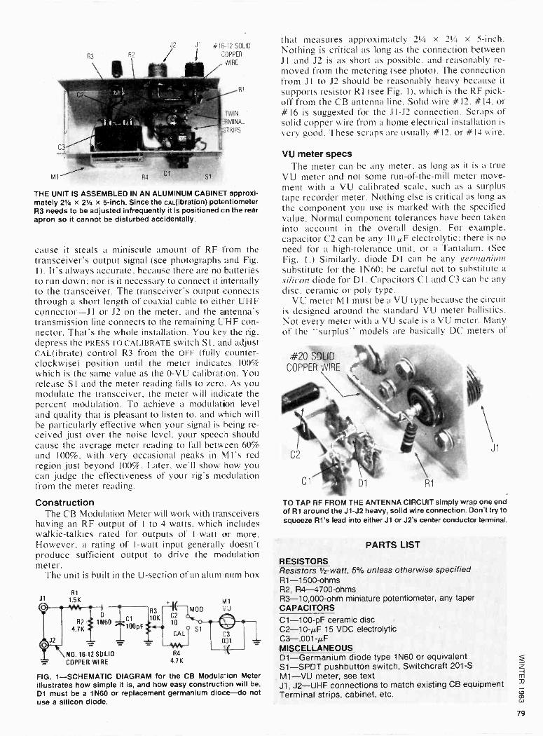
J2 J1 #16-12 SOLID
R3 R2 f
j COPPER
WIRE
R1
TWIN
MINAL
TRIPS
THE UNIT IS ASSEMBLED IN AN ALUMINUM CABINET approxi- mately 21/4 x 21/4 x 5 -inch. Since the cAL(ibration) potentiometer R3 needs to be adjusted infrequently it is positioned an the rear apron so it cannot be disturbed accidentally.
cause it steals a miniscule amount of RF from the transceiver's output signal (see photographs and Fig. 1). It's always accurate, because there are no batteries to run down; nor is it necessary to connect it internally to the transceiver. The transceiver's output connects through a short length of coaxial cable to either UHF connector-J1 or J2 on the meter, and the antenna's transmission line connects to the remaining UHF con- nector. That's the whole installation. You key the rig, depress the PRESS TO CALIBRATE switch S 1, and adjust CAL(ibrate) control R3 from the OFF (fully counter- clockwise) position until the meter indicates 100% which is the same value as the O -VU calibration. You release SI and the meter reading falls to zero. As you modulate the transceiver, the meter will indicate the percent modulation. To achieve a modulation level and quality that is pleasant to listen to, and which will be particularly effective when your signal is being re- ceived just over the noise level, your speech should cause the average meter reading to fall between 60% and 100%, with very occasional peaks in Ml's red region just beyond 100%. Later, we'll show how you can judge the effectiveness of your rig's modulation from the meter reading.
Construction The CB Modulation Meter will work with transceivers
having an RF output of 1 to 4 watts, which includes walkie-talkies rated for outputs of 1 -watt or more. However, a rating of 1 -watt input generally doesn't produce sufficient output to drive the modulation meter.
The unit is built in the U -section of an alumiinum box
J1 R1
1.5K
NO. 16-12 SOLID R4
COPPER WIRE 4.7K
FIG. 1-SCHEMATIC DIAGRAM for the CB Modulation Meter illustrates how simple it is, and how easy construction will be. D1 must be a 1N60 or replacement germanium diode-do not use a silicon diode.
that measures approximately 21/4 x 21/4 x 5 -inch. Nothing is critical as long as the connection between J1 and J2 is as short as possible, and reasonably re- moved from the metering (see photo). The connection from JI to J2 should be reasonably heavy because it supports resistor RI (see Fig. 1), which is the RF pick - off from the CB antenna line. Solid wire #12, #14, or #16 is suggested for the J1 -J2 connection. Scraps of solid copper wire from a home electrical installation is
very good. These scraps are usually #12, or #14 wire.
VU meter specs The meter can be any meter, as long as it is a true
VU meter and not some run-of-the-mill meter move- ment with a VU calibrated scale, such as a surplus tape recorder meter. Nothing else is critical as long as
the component you use is marked with the specified value. Normal component tolerances have been taken into account in the overall design. For example, capacitor C2 can be any 10µF electrolytic: there is no
need for a high -tolerance unit, or a Tantalum. (See
Fig. 1.) Similarly, diode DI can be any germanium substitute for the 1N60: be careful not to substitute a
silicon diode for DI. Capacitors C 1 and C3 can be any disc, ceramic or poly type.
VU meter MI must be a VU type because the circuit is designed around the standard VU meter ballistics. Not every meter with a VU scale is a VU meter. Many of the "surplus" models are basically DC meters of
#20 SOLID
COPPER WIRE
C2
Cl D1 R1
TO TAP RF FROM THE ANTENNA CIRCUIT simply wrap one end of R1 around the J1 -J2 heavy, solid wire connection. Don't try to squeeze Rl's lead into either J1 or J2's center conductor terminal.
PARTS LIST
RESISTORS Resistors 1/2 -watt, 5% unless otherwise specified R1 -1500 -ohms R2, R4 -4700 -ohms R3 -10,000 -ohm miniature potentiometer, any taper CAPACITORS
C1-100-pF ceramic disc C2 -10-µF 15 VDC electrolytic C3-.001 -µF MISCELLANEOUS Dl-Germanium diode type 1N60 or equivalent S1-SPDT pushbutton switch, Switchcraft 201-S Ml-VU meter, see text J1, J2-UHF connections to match existing CB equipment Terminal strips, cabinet, etc.
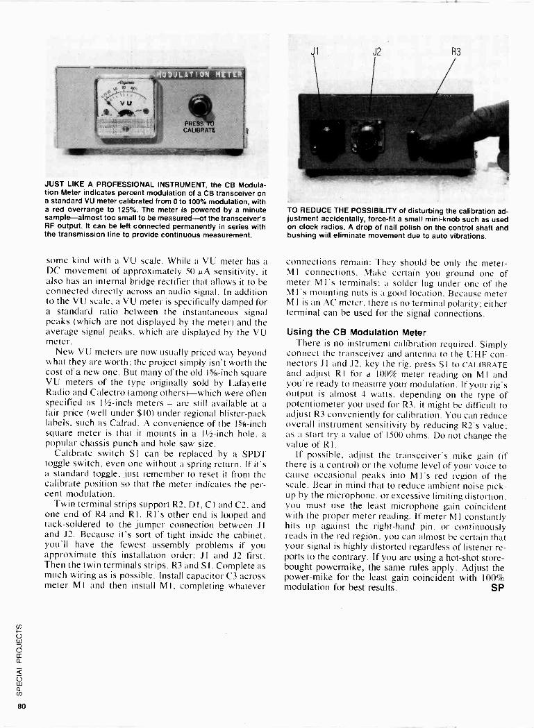
JUST LIKE A PROFESSIONAL INSTRUMENT, the CB Modula- tion Meter indicates percent modulation of a CB transceiver on a standard VU meter calibrated from 0 to 100% modulation, with a red overrange to 125%. The meter is powered by a minute sample-almost too small to be measured-of the transceiver's RF output. It can be left connected permanently in series with the transmission line to provide continuous measurement.
some kind with a VU scale. While a VU meter has a DC movement of approximately 50 µA sensitivity, it also has an internal bridge rectifier that allows it to be connected directly across an audio signal. In addition to the VU scale, a VU meter is specifically damped for a standard ratio between the instantaneous signal peaks (which are not displayed by the meter) and the average signal peaks, which are displayed by the VU meter.
New VU meters are now usually priced way beyond what they are worth; the project simply isn't worth the cost of a new one. But many of the old 15/8 -inch square VU meters of the type originally sold by Lafayette Radio and Calectro (among others)-which were often specified as 11/2 -inch meters- are still available at a fair price (well under $10) under regional blister -pack labels, such as Calrad. A convenience of the 15/s -inch square meter is that it mounts in a 11/ -inch hole, a popular chassis punch and hole saw size.
Calibrate switch SI can be replaced by a SPDT toggle switch, even one without a spring return. If it's a standard toggle, just remember to reset it from the calibrate position so that the meter indicates the per- cent modulation.
Twin terminal strips support R2. D1, C I and C2. and one end of R4 and R1. RI's other end is looped and tack -soldered to the jumper connection between JI and J2. Because it's sort of tight inside the cabinet, you'll have the fewest assembly problems if you approximate this installation order: JI and J2 first. Then the twin terminals strips, R3 and SI. Complete as much wiring as is possible. Install capacitor C3 across meter MI and then install M I , completing whatever
J1 J2 R3
TO REDUCE THE POSSIBILITY of disturbing the calibration ad- justment accidentally, force -fit a small mini -knob such as used on clock radios. A drop of nail polish on the control shaft and bushing will eliminate movement due to auto vibrations.
connections remain: They should be only the meter - M 1 connections. Make certain you ground one of meter Ml's terminals; a solder lug under one of the MI's mounting nuts is a good location. Because meter M 1 is an AC meter, there is no terminal polarity; either terminal can be used for the signal connections.
Using the CB Modulation Meter There is no instrument calibration required. Simply
connect the transceiver and antenna to the UHF con- nectors JI and J2, key the rig, press SI to CALIBRATE and adjust RI for a 100% meter reading on MI and you're ready to measure your modulation. If your rig's output is almost 4 watts, depending on the type of potentiometer you used for R3, it might be difficult to adjust R3 conveniently for calibration. You can reduce overall instrument sensitivity by reducing R2's value: as a start try a value of 1500 ohms. Do not change the value of RI.
If possible, adjust the transceiver's mike gain (if there is a control) or the volume level of your voice to cause occasional peaks into Ml's red region of the scale. Bear in mind that to reduce ambient noise pick- up by the microphone, or excessive limiting distortion. you must use the least microphone gain coincident with the proper meter reading. If meter MI constantly hits up against the right-hand pin, or continuously reads in the red region, you can almost be certain that your signal is highly distorted regardless of listener re- ports to the contrary. If you are using a hot -shot store- bought powermike, the same rules apply. Adjùst the power -mike for the least gain coincident with 100% modulation for best results. SP
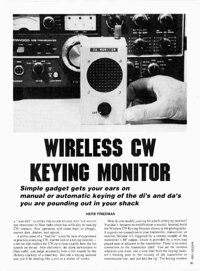
WIRELESS CW
KEYING MONITOR Simple gadget gets your ears on manual or automatic keying of the di's and da's you are pounding out in your shack
HERB FRIEDMAN
A "BAD FIST" IS OFTEN THE MAJOR REASON WHY THE NOVICE
and newcomer to Ham radio often has difficulty in making CW contacts. Few operators will come back to choppy, uneven dots, dashes, and spaces.
A prime cause of a "bad fist" is not the lack of experience or practice at sending CW, but the lack of a keying monitor- a device that enables the CW op to hear exactly how the fist sounds on the air. Few old-timers, let alone newcomers to Ham radio, can judge accurately how a fist sounds by the clickety-clackety of a hand key. But use a keying monitor and you'll be sending like a pro in a matter of weeks.
How do you modify your rig for a built-in keying monitor? You don't, because no modification is needed. Instead, build the Wireless CW Keying Monitor shown in the photographs. It requires no connection to your transmitter, transceiver, or receiver because it's triggered by a minute sample of the transmitter's RF output, which is provided by a wire lead placed near or adjacent to the transmitter. There is no direct connection to the transmitter itself. You set the monitor wherever you want, run a wire lead from the keying moni- tor's binding post to the vicinity of the transmitter or transmission line, and just key the rig. The keying monitor
81
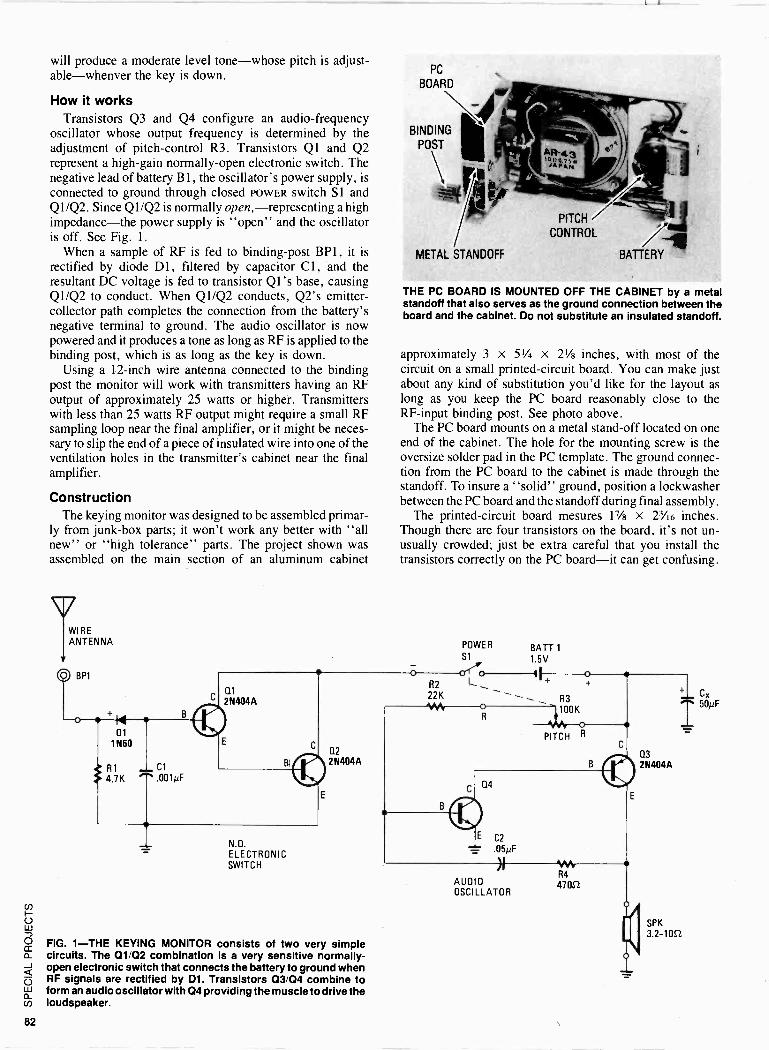
will produce a moderate level tone-whose pitch is adjust- able-whenver the key is down.
How it works Transistors Q3 and Q4 configure an audio -frequency
oscillator whose output frequency is determined by the adjustment of pitch -control R3. Transistors Q1 and Q2 represent a high -gain normally -open electronic switch. The negative lead of battery B1, the oscillator's power supply, is connected to ground through closed POWER switch S 1 and Ql/Q2. Since Q1/Q2 is normally open,-representing a high impedance-the power supply is "open" and the oscillator is off. See Fig. 1.
When a sample of RF is fed to binding -post BPI, it is rectified by diode D1, filtered by capacitor Cl, and the resultant DC voltage is fed to transistor Q1's base, causing Q1/Q2 to conduct. When Q1/Q2 conducts, Q2's emitter - collector path completes the connection from the battery's negative terminal to ground. The audio oscillator is now powered and it produces a tone as long as RF is applied to the binding post, which is as long as the key is down.
Using a 12 -inch wire antenna connected to the binding post the monitor will work with transmitters having an RF output of approximately 25 watts or higher. Transmitters with less than 25 watts RF output might require a small RF sampling loop near the final amplifier, or it might be neces- sary to slip the end of a piece of insulated wire into one of the ventilation holes in the transmitter's cabinet near the final amplifier.
Construction The keying monitor was designed to be assembled primar-
ly from junk -box parts; it won't work any better with "all new" or "high tolerance" parts. The project shown was assembled on the main section of an aluminum cabinet
WIRE ANTENNA
BP1
N.O. ELECTRONIC SWITCH
FIG. 1-THE KEYING MONITOR consists of two very simple circuits. The 01 /02 combination is a very sensitive normally - open electronic switch that connects the battery to ground when RF signals are rectified by D1. Transistors 03/04 combine to form an audio oscillator with 04 providing the muscle to drive the loudspeaker.
PC
BOARD
BINDING
POST
PITCH
CONTROL
METAL STANDOFF BATTERY
THE PC BOARD IS MOUNTED OFF THE CABINET by a metal standoff that also serves as the ground connection between the board and the cabinet. Do not substitute an insulated standoff.
approximately 3 x 51/4 x 21/4 inches, with most of the circuit on a small printed -circuit board. You can make just about any kind of substitution you'd like for the layout as long as you keep the PC board reasonably close to the RF -input binding post. See photo above.
The PC board mounts on a metal stand-off located on one end of the cabinet. The hole for the mounting screw is the oversize solder pad in the PC template. The ground connec- tion from the PC board to the cabinet is made through the standoff. To insure a "solid" ground, position a lockwasher between the PC board and the standoff during final assembly.
The printed -circuit board mesures l'/s x 23/16 inches. Though there are four transistors on the board, it's not un- usually crowded; just be extra careful that you install the transistors correctly on the PC board-it can get confusing.
R2
22K
POWER
S1
BATT 1
1.5V
o i + +
j100K
04
E C2 y .05µF
)1
AUDIO OSCILLATOR
PITCH R
NM, R4
47052
Q3
2N404A
SPK 3.2-1022
82
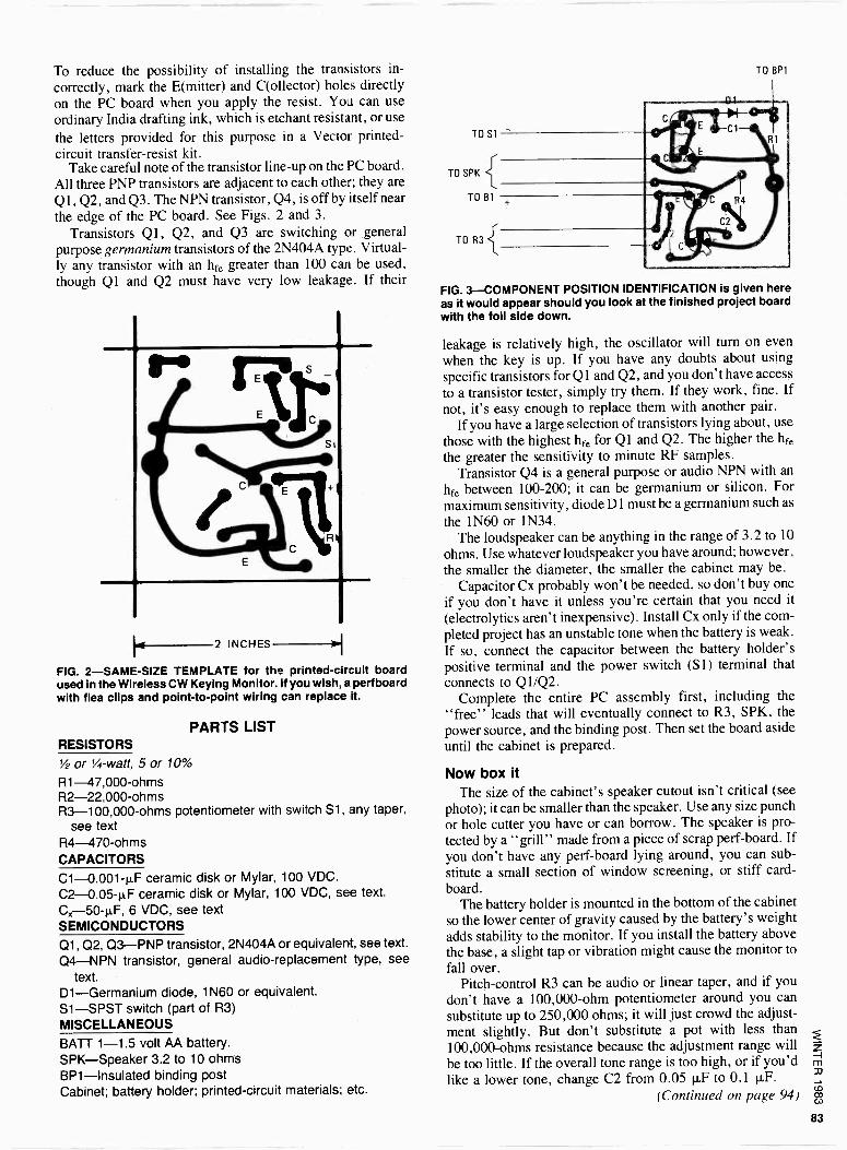
To reduce the possibility of installing the transistors in-
correctly, mark the E(mitter) and C(ollector) holes directly on the PC board when you apply the resist. You can use ordinary India drafting ink, which is etchant resistant, or use
the letters provided for this purpose in a Vector printed - circuit transfer -resist kit.
Take careful note of the transistor line-up on the PC board. All three PNP transistors are adjacent to each other; they are
Q1, Q2, and Q3. The NPN transistor, Q4, is off by itself near the edge of the PC board. See Figs. 2 and 3.
Transistors Q1, Q2, and Q3 are switching or general purpose germanium transistors of the 2N404A type. Virtual- ly any transistor with an hfe greater than 100 can be used, though Q1 and Q2 must have very low leakage. If their
14--2 INCHES -01
FIG. 2-SAME-SIZE TEMPLATE for the printed -circuit board used in the Wireless CW Keying Monitor. If you wish, a perfboard with flea clips and point-to-point wiring can replace it.
PARTS LIST RESISTORS
1/2 or 1/4 -watt, 5 or 10%
R1 -47,000 -ohms R2 -22,000 -ohms R3 -100,000 -ohms potentiometer with switch S1, any taper,
see text R4 -470 -ohms CAPACITORS C1-0.001-1.LF ceramic disk or Mylar, 100 VDC. C2 -0.05-µF ceramic disk or Mylar, 100 VDC, see text.
Cx-50-µF, 6 VDC, see text SEMICONDUCTORS
01, Q2, Q3-PNP transistor, 2N404A or equivalent, see text.
04-NPN transistor, general audio -replacement type, see
text. Dl-Germanium diode, 1N60 or equivalent. S1-SPST switch (part of R3) MISCELLANEOUS
BATT 1-1.5 volt AA battery. SPK-Speaker 3.2 to 10 ohms BP1-Insulated binding post Cabinet; battery holder; printed -circuit materials; etc.
TO BPI
TO Si
TO SPK
TO 131
TO R3 {
FIG. 3-COMPONENT POSITION IDENTIFICATION is given here as it would appear should you look at the finished project board with the foil side down.
leakage is relatively high, the oscillator will turn on even
when the key is up. If you have any doubts about using specific transistors for Q1 and Q2, and you don't have access to a transistor tester, simply try them. If they work, fine. If
not, it's easy enough to replace them with another pair. If you have a large selection of transistors lying about, use
those with the highest hfe for Q1 and Q2. The higher the hfe
the greater the sensitivity to minute RF samples. Transistor Q4 is a general purpose or audio NPN with an
hfe between 100-200; it can be germanium or silicon. For
maximum sensitivity, diode D1 must be a germanium such as
the 1N60 or 1N34. The loudspeaker can be anything in the range of 3.2 to 10
ohms. Use whatever loudspeaker you have around; however, the smaller the diameter, the smaller the cabinet may be.
Capacitor Cx probably won't be needed, so don't buy one if you don't have it unless you're certain that you need it
(electrolytics aren't inexpensive). Install Cx only if the com- pleted project has an unstable tone when the battery is weak. If so, connect the capacitor between the battery holder's positive terminal and the power switch (S1) terminal that connects to Q1/Q2.
Complete the entire PC assembly first, including the "free" leads that will eventually connect to R3, SPK, the
power source, and the binding post. Then set the board aside until the cabinet is prepared.
Now box it The size of the cabinet's speaker cutout isn't critical (see
photo); it can be smaller than the speaker. Use any size punch or hole cutter you have or can borrow. The speaker is pro- tected by a "grill" made from a piece of scrap perf-board. If you don't have any perf-board lying around, you can sub- stitute a small section of window screening, or stiff card- board.
The battery holder is mounted in the bottom of the cabinet so the lower center of gravity caused by the battery's weight adds stability to the monitor. If you install the battery above the base, a slight tap or vibration might cause the monitor to
fall over. Pitch -control R3 can be audio or linear taper, and if you
don't have a 100,000 -ohm potentiometer around you can
substitute up to 250,000 ohms; it will just crowd the adjust- ment slightly. But don't substitute a pot with less than 100,000 -ohms resistance because the adjustment range will
be too little. If the overall tone range is too high, or if you'd like a lower tone, change C2 from 0.05 µF to 0.1 F.
(Continued on page 94)
AIR BURST ETCHING Cut your etching time by one-half or more and improve printed -circuit board quality by putting thousands of little air bubbles to work.
HERB FRIEDMAN
PHOTO -FINISHERS HAVE LONG KNOWN THEY CAN GET better negative development by bubbling an inert gas through the developer. The reason why it works better is that the gas, which is usually nitrogen, agitates the developing solution as it bubbles up to the top of the chemical tank. That insures freedom from air pockets on the film itself; faster development, because ex- hausted developer is constantly replenished at the film boundary, and a more even development, because the developer is flowing constantly across the entire sur- face. The burst process is called Nitrogen Burst Developing.
A burst etching tank for your printed -circuit boards will give you almost the same advantages-even more -and you can use ordinary air for the burst gas. In fact, you can build a complete air -burst etching system for about $15, and that includes the air pump.
Why air burst? The quick -and -dirty way for the hobbyist to make
single PC boards is to apply a resist pattern directly to
the copper foil, and then etch 'away the unprotected copper by immersing the copper -clad board in a rela- tively mild acid called an etchant (available under the Vector and GC labels, among others). Within a room temperature range of approximately 70°F to 75°F it takes about 45 to 90 minutes to etch a small board. If the etchant's temperature is below 70°F it could take as much as 2 hours to etch a small PC board. And those timings assume almost constant agitation to insure that there are no air pockets between the copper and the etchant. (Air pockets result in small circles of copper that must be removed from the board by hand, using a knife, chisel, or hand grinder.)
By using the continuous air bubbles to produce con- stant agitation throughout the etchant, you can cut etching time down to 10 minutes for small boards, and produce razor-sharp foils with no copper circles caused by air bubbles. Even well -used etchant at 65 to 68 degrees can produce a fully etched board in as little as 20 minutes, again with no air pockets to worry about.
FIG. 1-HERE'S WHAT YOU NEED to make your own air -burst etching system. A plastic tray, plastic tubing, a small fish -tank air pump, some adhesive, and a "grease pencil."
FIG. 2-TO SEAL THE END of the plastic tubing, place a drop of plastic cement in the tubing, invert quickly, and clamp the end in a vise until the cement dries. Don't use too much cement.
84
The parts for an air -burst etching system suitable for hobbyists costs less than $15 if you have the required adhesives. If not, figure a few dollars more. The basic system consists of the smallest possible "fish tank" air pump, 4 to 5 feet of soft 3/16 -inch plastic tubing (avail- able from larger hardware stores) and one or more Rubbermaid plastic trays, the type used to store cutlery in kitchen cabinets. The 3W x 9L x 2H -inch tray shown in the photos is perfect for small PC boards. The double -size 6 x 9 x 2 -inch tray is recommended for larger boards. (Always use the smallest possible tray for the job.)
The pump size is extremely important: If it's too powerful it will splash . etchant for several feet, and doesn't necessary produce a better board. The model you need is sold under various "private labels." It pumps just about enough air for a single small goldfish in a small bowl. It has no "cubic -feet -per -minute" rat- ing. It's just small and cheap. usually $9.95 listl(top price you should pay).
The PVC tubing must be soft and 3/I6 inch. Do not use the semi -rigid tubing usually sold in pet stores for "fish tanks." It's not 3/16 -inches, and causes more in- stallation -and -use problems than it's worth. Get the right stuff in a hardware store. It's about 25 cents a foot, top price. Four feet is fine for a small tray; use 5 feet for a large tray.
Build your etcher The photos show how to build your air -burst etcher.
In addition to the pump, the tubing, and the tray, you'll need some contact adhesive and one of the new fast drying all-purpose "plastic" cements (glue) such as Weldit. See Fig. I. Don't try to have the contact adhe- sive do double -duty; you must use both adhesives, because the etchant appears to "attack" the contact cement, causing it to loosen it's grip.
The first step is to seal the end of the tubing. Place a drop of plastic cement (Weldit) in the tubing, invert the tubing quickly and clamp about 1/4 -inch of the end in a vise. See Fig. 2. Allow the tubing to "set" at least 24 hours, longer if the adhesive appears "wet." The more adhesive you use, the longer it takes to cure.
When the cement is dry, force the tubing into the tray
so that it forms a gentle serpentine pattern, as shown in Fig. 3. One -and -a -half sine waves is sufficient. Force the sealed end of the tubing into one corner of the tray and route the tubing up and out from the opposite corner on the same side of the tray. Using a "grease" pencil-also known as a "China Marker"-trace the outline of the tubing in the bottom of the tray and then remove the tubing.
Next, lay down a thin strip of contact cement on the pencil outline and coat a strip of cement along the tubing. Allow both to set until they are dry to the touch. Be extremely careful now, because the contact adhe- sive does not permit repositioning; force the sealed end of the tubing into the corner -of the tray and apply the tubing along the pencil outline. routing the tubing up and out the opposite corner. Don't worry if the tubing isn't too secure; the contact adhesive is only to hold it in place for the final gluing. See Fig. 4.
Next pack in the cement by forcing the nozzle of the cement tube into the tubing/tray joint. See Fig. 5. If necessary, spread the cement with a toothpick or a screwdriver, so that the tubing is cemented its entire length on both sides. It will look messy, but so what! Don't forget to cement the vertical rise of the tubing at the corner where it exits from the tray. Let the cement dry overnight.
Using a No. 16 or No. 14 sewing -machine needle- not a straight needle or pin-punch a series of holes along the top of the tubing spaced 3/4 -inch to 1 -inch apart. See Fig. 6. Don't overdo the holes. If you have too many too close, you get excessive acid splash. Push the needle through the tubing until you see the "eye" go through (don't worry if the needle bottoms); then twist the needle once or twice, so the edges of the "eye" cut the tubing, and then remove the needle. That's the whole bit. The Air -Burst Etcher is ready for use. Checkout and put it to work
Place the tray in the center of several sheets of paper toweling, preferably Bounty. (I don't know how Bounty works in the kitchen, but it's tops in the dark- room for mopping up chemical and acid spills.) Connect the tubing to the pump output. Fill the tray about half- way with water and plug in the pump. See Fig. 7. Observe the bubbles at the surface of the water; they
FIG. 3-FORCE THE TUBING INTO THE TRAY in 3 serpentine pattern and trace the outline with a grease pencil. Make 11/2 "S" turns in a small tray-more are required in larger trays.
FIG. 4-APPLY A THIN STRIP OF CONTACT CEMENT along the pencil outline and a strip along the plastic tubing. Wait for the cement to get tacky before proceeding to the next step.
85
FIG. 5-FORCE THE PLASTIC TUBING into the contact adhesive following the pencil outline and then pack both sides of the tubirg where it meets the tray with the plastic cement.
FIG. 6-USING A NO. 16 OR NO. 14 sewing machine needle. pierce the air holes in the plastic tubing spaced at 3/4 inch to 1
inch apart, along the tubing's length that is cemented to the bottom of the tray.
won't be evenly distributed throughout the surface, but they should be more or less even along the serpentine shape of the tubing. See Fig. 8. If not, some of the holes in the tubing are clogged (poor punching), simply punch others through the water.
Fill the tray about 3/4 full with etchant and plug in the pump. Make certain that you have the tray on paper toweling because there is some etchant spray, which tends to stain if it gets on cloth, wood, or porcelain. Float your PC board on top of etchant. (Use photo- graphic tongs to position the board.) The air burst will "blast" out any air pockets. If the board is too heavy to float, place a few wood clothespins in the tray so that the board can be supported at an angle with one edge on the bottom of the tray and the other resting on a clothes- pin. You might have to change the position of the board a few times to insure an even removal of the copper. Generally, the board will float.
If you're using fresh etchant, check the board after 10 minutes and every minute or so thereafter. If it's used etchant, check after 15 minutes and every five
minutes thereafter. If a board takes longer than 30 minutes, either the temperature is too low (below 65°F) or the etchant is exhausted.
Don't worry about color The etchant causes severe discoloration of the con-
tact adhesive and some softening of the tubing. Don't worry about the discoloration; it does no harm. The softening of the tubing can result in some of the air holes closing after the system has been used three or four times. If that happens, simply punch a few new holes in the tubing. (Use water for the testing and punching.) Eventually the tubing stabilizes and you won't have to punch any more new holes.
If you see that some holes are clogged after you have poured the etchant, simply forget about it until you're finished. Just position the board over whatever air burst there is.
Always remember to flush out the tray, and the sur- face of the tubing, with running water when you're finished. SP
FIG. 7-TO ETCH .A BOARD, fill the tray 3,4 full with etchant. Attach the air pump and power it up. Float the board on top of the etchent face down for the time period prescribed in the text.
FIG. 8-IF AFTER A FEW USES air bursts appears at only one or two locations, some of the air holes are blocked. New air holes should be punched after the etchant is removed.
86

TEMP -SENSOR D. E. PATRICK
BUILD A TEMPERATURE -SENSITIVE PROBE (WE CALL IT TEMP - Sensor) for your DVM or DMM, for only $20 or less, and enjoy fantastic accuracy and wide operating range.. You can enjoy specs like up to ± 2% accuracy, ± .8% nonlinearity, operating over the range from - 55° C to + 150° C ( - 132° F to + 302° F). Using only one or two inexpensive IC's the probe can give direct readings in Fahrenheit (°F), Celsius or Centigrade (°C), Kelvin (°K) or Rankine (°R) In this text we will refer to Celsius in place of Centrigrade, in accord with the scientific community's international agreement in 1948.
The simple circuits presented in Figs. 1 and 2 are built around Analog Devices; AD590K temperature transducer
TABLE I
TEMPERATURE SCALE CONVERSIONS
Fahrenheit Rankine Celsius Kelvin (°F) (°R) (°C) (°K)
212 672 100 373 Boiling Point of Water 122 580 50 323 68 527 20 293 32 491 0 273 Freezing Point of Water
-148 311 -100 173 -297 162 -183 90 Boiling Point of Oxygen -452 8 -269 4 Boiling Point of Helium -460 0 -273 0 Absolute Zero
The Fahrenheit scale divides the difference between the freezing point of water at 32° F and the boiling point at 212° F into 180 degress. The Centigrade or Celsius scale divides the scale from freezing to boiling into 100 steps or degrees from 0° C to 100° C. But, where the references for Fahrenheit and Centigrade are the freezing point of water under standard atmospheric pressure, the reference starting point for the Kelvin and Rankine scales is absolute zero. The value for absolute zero per °F and °C are rounded off to the nearest degree.
and AD580J 2.5 -volt DC reference. The AD590J/K/L/ series of Proportional To Absolute Temperature (PTAT) current regulators, similar to the National LM134/234/334/ series, don't have a troublesome current setting third terminal. But, the Analog Devices' PTAT's have better specs and are more workable. However, as with the LM134 series, where the normal output is proportional to the absolute -Kelvin (°K) temperature scale, we must convert the normal 1µA/°K (microAmpere-per-degree Kelvin) output for a direct readout in °C, °F, or °R.
The temperature scales From Table 1, we can see that the Fahrenheit t°F) scale
divides the difference between the reference temperature of 32° F, the freezing point of water under standard atmospheric pressure, into 180 degrees before the boiling point is reached at 212° F. The Celsius (°C) scale divides the difference from freezing to boiling into 100 steps, or degrees, from 0° C to 100° C. And we can convert from Celcius to Farhenheit and back again by the two simple equations shown below in Table 2.
Now, that brings us to the absolute temperature scales of Kelvin (°K) and Rankine (°R), which may be of little value to the average user, unless you're interested in cryogenics, superfluids, or superconductors. However, from a practical standpoint, we need to know something about them, if we're going to talk intelligently about converting from one tem- perature scale to the other.
TABLE 2
Temperature Scales Conversion Equations
Fahrenheit to Celsius C = 5/9(F-32)
Celsius to Kelvin K = C -273
Celsius to Fahrenheit F = 9/5C +32
Rankine to Kelvin R = 5/9R
Kelvin to Celsius C=K-273
Kelvin to Rankine R=9/5K
Degree symbol (°) has been deleted for clarity Thus: °C = C, °F = F, etc.
Theoretically, the lowest possible temperature is believed by scientists to be -273.16° C or - 459.6° F, a point which can be approached, but never reached, and a point at which it is said a body has lost all the heat (or energy) it is possible to give up. That theoretical point-theoretical because you cannot get there from here (also referred to as "absolute zero")-is the reference starting point of the Kelvin tem- perature scale.
A Kelvin degree represents the same temperature change as a Celsius degree, where K = C + 273 and C = K - 273, approximately. For simplicity sake, the absolute values of °C and °F scales are rounded off to - 273 and - 460, respective- ly. But, the Kelvin scale, which simplifies solving problems dealing with changes in gas volumes at low temperatures, need only be understood here, in terms of its relationship to the Celsius scale.
On the other hand, the Rankine temperature scale is to the Kelvin scale, what the Celsius scale is to the Fahrenheit
Your DVM can read out temperatures from -132° F to 302° F
with an overall accuracy of +2 percent
AD590K PTAT
+5V
R1
(1.75K) 950S2
R2 (200)
10012
I I II I -. DVM/DMM
o o
FIG. 1-SCHEMATIC DIAGRAM of Proportional -To-Absolute Temperature (PTAT) probe circuit used to provide an analog output current proportional to Kelvin and Rankine temperature scales. Values in parentheses are for Rankine measurements.
PTAT AD590K
AD580J 2.5 VDC REFERENCE íOU
(1.8K) 1K
I-I I-1 I I
DVM/DMM o 0 + - R5
(1.95K) 1K
R3
(9.53K) 9.09 K
E -E
+5V REGULATED OR UNREGULATED
FIG. 2-SCHEMATIC DIAGRAM OF TEMP -SENSOR circuit with conversion from Kelvin -to -Celsius (Rankine -to-Fahrenheit) tem- perature scales. Values in parentheses are for Rankine -to- Fahrenheit measurements.
R4
(500) 200
VOFF ADJ.
scale. That is, a Rankine degree is the same size as a Fahrenheit degree, and a Kelvin degree is the same size as a Celsius degree. Therefore, we need only apply the simple conversion equations, summarized in Table 2 and discussed in the text, to convert from a 1µA/°K output to a direct readout in °R. Then to convert °R to other temperature scales, the formulas given in Table 2 should be used.
THE AUTHOR'S PROTOTYPE TEMP -SENSOR unit is shown here. The unit is housed in a glass thermometer case, but a plastic gravy serving syringe can do the job. Just remove the rubber bulb. The syringe is available in most Woolco stores.
VREF = 2.5V
RT =R3+R4+R5
IT = VREF/Rr
ER3 =1, x R3
E24 = IT x R4 Ve = 2.43mV-
ER5 = li x 135
ER = ER3 + ER4 + ER5 VREF
VA = VREF - ER3
VB VREF - ER3 - ER4
VR4RANGE = VA - V,
VA = 292mV -
VA - ER4
R3 9.09K
ER3 =
R4 2000 ER4 =
R5 1K
ER5
VREF = 2.5V
R3
9.53K
2.208V ER3 = 1.989V VA= 511mV-
R4 500
049V ER4 = 104V VB = 407mV-
R5 1.95K
.243V ERS = .407V
FIG. 3-EQUATIONS REQUIRED TO RECALCULATE resistances values for networks in Fig. 2.
= D2
íN914
PTAT AD590K
R1
950 SZ
VN
I-I I-I I-I I_I I_I
R3
D1 20K =1N914 -*OA
EouT
DVM/DMM 0 o
®
r V1h R4
5K
VOFF
AD580J 2.5 VDC REFERENCE
S1
BATT1 9VOC
+;)1
FIG. 4-AN ALTERNATE VARIABLE Temp -Sensor hookup which provides for a wide range of adjustment. D1 and D2 are added to reduce thermal effects and power -dissipation caused power supply rated in excess of 5 VDC.
Putting it all together In Fig. 1, the AD590K temperature transducer provides a
current that is directly proportional to absolute temperature value at a rate of 1 µA/°K. The output current develops a voltage determined by RI and R2 in series. Thus, giving that a current of 1µA/°K will flow through R1 and R2, when the series combination is trimmed to approximately 1000 ohms, lmV/°K will be developed across the resistors. The trimming is required, because the AD590K has an absolute error of ±5.5% C maximum without a calibration adjustment and only a ± 2.0° C maximum error when properly adjusted. In any case, a DVM or DMM placed across R1 and R2, on its milliVolt scale, would read temperature in °K, such that
Vt = (R1 + R2) (1µA/°K). Now from the equation in Table 2, where R = 9/5K or
1.8K, it follows, that if we make the series combination of R1 + R2 = 1.8K, the 1µA/°K output of the AD590K would develop 1.8 mV/°K for a direct conversion to a Rankine temperature scale output.
Also, in Fig. 2, for an output proportional to the Celsius temperature scale, we apply equation C = K - 273, where subtracting or offsetting V, = 1 mV/°K by 273 mV will give us a scale factor of 1 mV/°C. The AD580J provides us with a stable 2.5 volt DC reference and resistors R3, R4, and R5 gives an adjustable Vat- from approximately 243 mV to 292 mV for the resistive values shown. However, the man -
88
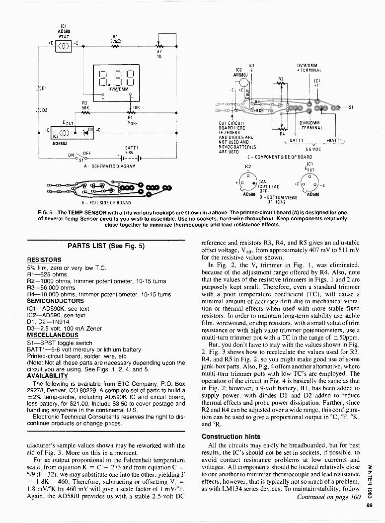
'Cl AD590 PTAT R1
BATT1
ON OFF 5-6V
A - SCHEMATIC DIAGRAM
cc co a°O.ál; 000
B - FOIL SIDE OF BOARD
ICI IC2 -E
AD580J R2
0 I II CUT CIRCUIT I DVM DMM
BOARD HERE -TERMINAL IF ZENERS R4 AND DIODES ARE NOT USED AND \ -BATT 1 +BAIT 1
DVM/OMM +TERMINAL
5-SVDC BATTERIES 5-6 VDC
ARE USED
C - COMPONENT SIDE OF BOARD
IC2 ICI
AD580 0 - BOTTOM VIEWS
OF IC1.2
CAN (CUT LEAD OFF)
Eour
AD590
-E
FIG. 5-The TEMP -SENSOR with all its various hookups are shown in a above. The printed -circuit board (b) is designed for one of several Temp -Sensor circuits you wish to assemble. Use no sockets; hard -wire throughout. Keep components relatively
close together to minimize thermocouple and lead resistance effects.
PARTS LIST (See Fig. 5)
RESISTORS 5% film, zero or very low T.C. R1-825 ohms R2-1000 ohms, trimmer potentiometer, 10-15 turns R3-56,000 ohms R4-10,000 ohms, trimmer potentiometer, 10-15 turns SEMICONDUCTORS IC1-AD590K, see text IC2-AD590, see text D1, D2 -1N914 D3-2.5 volt, 100 mA Zener MISCELLANEOUS S1-SPST toggle switch BATT1-5-6 volt mercury or lithium battery Printed -circuit board, solder, wire, etc. (Note: Not all these parts are necessary depending upon the circuit you are using. See Figs. 1, 2, 4, and 5. AVAILABILITY
The following is available from ETC Company. P.O. Box 29278, Denver, CO 80229. A complete set of parts to build a ±2% temp -probe, including AD590K IC and circuit board, less battery, for $21.00. Include $3.50 to cover postage and handling anywhere in the continental U.S.
Electronic Technical Consultants reserves the right to dis- continue products or change prices.
ufacturer's sample values shown may be reworked with the aid of Fig. 3. More on this in a moment.
For an output proportional to the Fahrenheit temperature scale, from equation K = C + 273 and from equation C = 5/9 (F - 32), we may substitute one into the other, yielding F = 1.8K -460. Therefore, subtracting or offsetting V, = 1.8 mV/°K by 460 mV will give a scale factor of 1 mV/°F. Again, the AD580J provides us with a stable 2.5 -volt DC
Si
reference and resistors R3, R4, and R5 gives an adjustable offset voltage, Voff, from approximately 407 mV to 511 mV for the resistive values shown.
In Fig. 2, the Vt trimmer in Fig. 1, was eliminated, because of the adjustment range offered by R4. Also, note that the values of the resistive trimmers in Figs. 1 and 2 are purposely kept small. Therefore, even a standard trimmer with a poor temperature coefficient (TC), will cause a minimal amount of accuracy drift due to mechanical vibra- tion or thermal effects when used with more stable fixed resistors. In order to maintain long-term stability use stable film, wirewound, or chip resistors, with a small value of trim resistance or with high value trimmer potentiometers, use a multi -turn trimmer pot with a TC in the range of ± 50ppm.
But, you don't have to stay with the values shown in Fig. 2. Fig. 3 shows how to recalculate the values used for R3, R4, and R5 in Fig. 2, so you might make good use of some junk -box parts. Also, Fig. 4 offers another alternative, where multi -turn trimmer pots with low TC's are employed. The operation of the circuit in Fig. 4 is basically the same as that in Fig. 2; however, a 9 -volt battery, B 1, has been added to supply power, with diodes D1 and D2 added to reduce thermal effects and probe power dissipation. Further, since R2 and R4 can be adjusted over a wide range, this configura- tion can be used to give a proportional output in °C, °F, °K, and °R.
Construction hints All the circuits may easily be breadboarded, but for best
results, the IC's should not be set in sockets, if possible, to avoid contact resistance problems at low currents and voltages. All components should be located relatively close to one another to minimize thermocouple and lead resistance effects, however, that is typically not so much of a problem, as with LM134 series devices. To maintain stability, follow
Continued on page 100
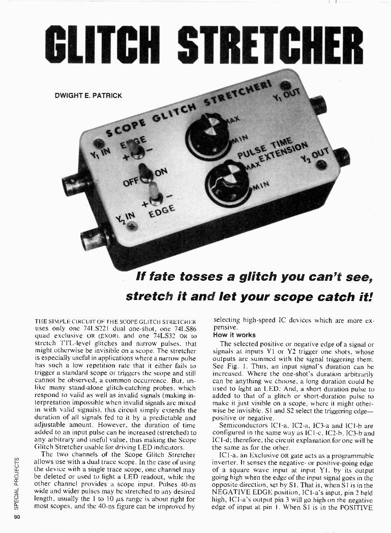
GLITCH STRETCHER DWIGHT E. PATRICK EtR% 4:0 Rt `tt
If fate tosses a glitch you can't see, stretch it and let your scope catch it!
THE SIMPLE CIRCUIT OF THE SCOPE GLITCH STRETCHER uses only one 74LS221 dual one-shot, one 74LS86 quad exclusive OR (EXOR), and one 74LS32 OR to stretch TTL-level glitches and narrow pulses, that might otherwise be invisible on a scope. The stretcher is especially useful in applications where a narrow pulse has such a low repetition rate that it either fails to trigger a standard scope or triggers the scope and still cannot be observed, a common occurrence. But, un- like many stand-alone glitch -catching probes, which respond to valid as well as invalid signals (making in- terpretation impossible when invalid signals are mixed in with valid signals), this circuit simply extends the duration of all signals fed to it by a predictable and adjustable amount. However, the duration of time added to an input pulse can be increased (stretched) to any arbitrary and useful value, thus making the Scope Glitch Stretcher usable for driving LED indicators.
The two channels of the Scope Glitch Stretcher allows use with a dual trace scope. In the case of using the device with a single trace scope, one channel may be deleted or used to light a LED readout, while the other channel provides a scope input. Pulses 40-ns wide and wider pulses may be stretched to any desired length, usually the 1 to 10 µs range is about right for most scopes, and the 40-ns figure can be improved by
selecting high-speed IC devices which are more ex- pensive. How it works
The selected positive or negative edge of a signal or signals at inputs Y l or Y2 trigger one shots, whose outputs are summed with the signal triggering them. See Fig. 1. Thus, an input signal's duration can be increased. Where the one -shot's duration arbitrarily can be anything we choose, a long duration could be used to light an LED: And, a short duration pulse to added to that of a glitch or short -duration pulse to make it just visible on a scope, where it might other- wise be invisible. S l and S2 select the triggering edge- positive or negative.
Semiconductors IC 1-a, IC2-a, IC3-a and IC 1-b are configured in the same way as IC 1-c, IC2-b, IC3-b and IC 1-d; therefore, the circuit explanation for one will be the same as for the other.
ICI -a, an Exclusive OR gate acts as a programmable inverter. It senses the negative- or positive -going edge of a square wave input at input Y 1, by its output going high when the edge of the input signal goes in the opposite direction, set by S 1. That is, when Sus in the NEGATIVE EDGE position, ICI-a's input, pin 2 held high, IC 1-a's output pin 3 will go high on the negative edge of input at pin 1. When Si is in the POSITIVE
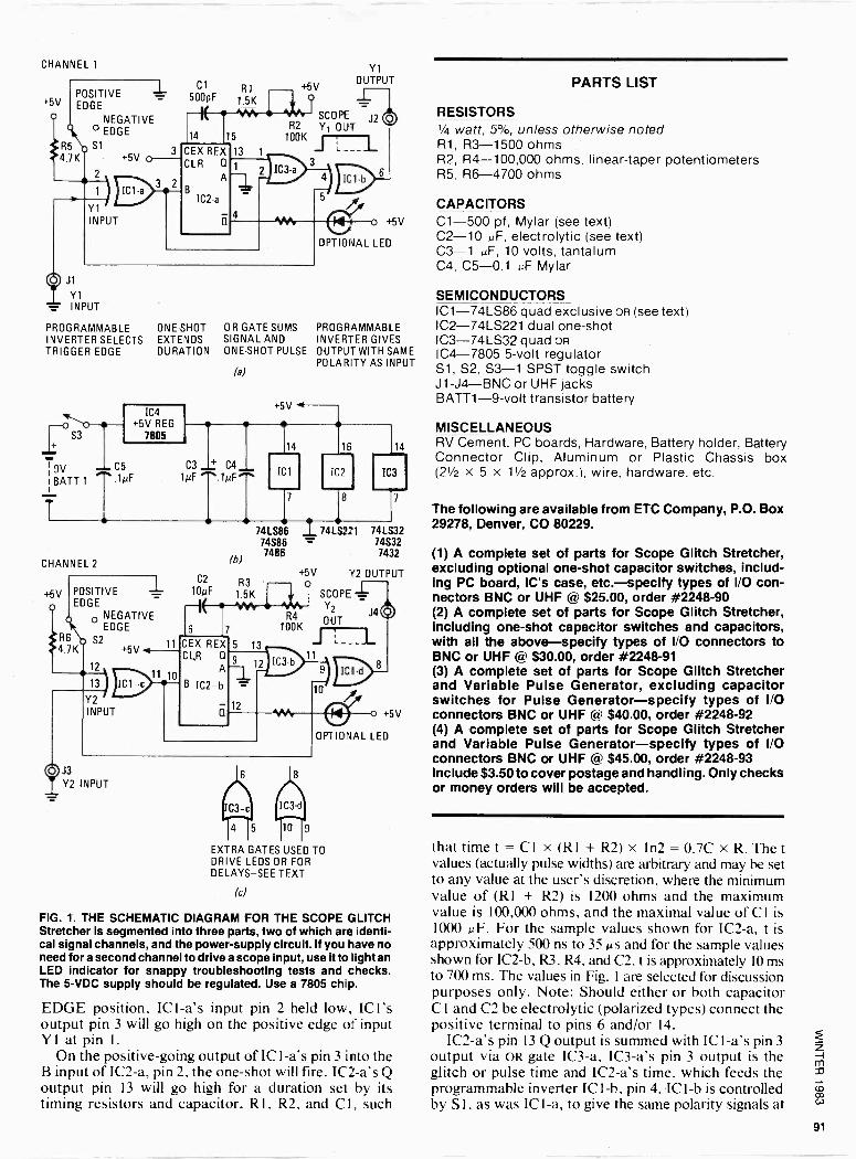
+5V
o
R5
4.7 K
POSITIVE EDGE
NEGATIVE EDGE
S1
+5V o- 3 Y1
INPUT
1
3 2
f
Cl 500pF
14
CEX REX CLR O
A B
IC2-a
R1
1.5K
15
13 1
1
4
+5V
Y1
OUTPUT
SCOPE J2 R2 Y1 OUT
100K
3
a
FN o +5V
OPTIONAL LED
4 J1
Y1 INPUT
PROGRAMMABLE INVERTER SELECTS TRIGGER EDGE
S3
9V BATT 1
T
ONE-SHOT EXTENDS DURATION
OR GATE SUMS PROGRAMMABLE SIGNAL AND INVERTER GIVES ONE-SHOT PULSE OUTPUT WITH SAME
POLARITY AS INPUT (al
IC5 C3 + C4 1 IC2 IC3
T.1µF 1µF .1µF
+5V<
CHANNEL 2
+5V
o
R6
1
IC4 +5V REG
1805
j
POSITIVE y C2
_ 10µF EDGE
NEGATIVE EDGE 6
4 4.7K S2
12 13 IIC1 -c
Y2 INPUT
7
+5V .4 11 CEX REX
CLR A
IC2-b 11 1
(b)
R3 1.5K
14 16 114
IC
74LS86 I 74LS221 74LS32 74S86 = 74S32 7486 7432
+5V Y2 OUTPUT o
SCOPEY2 _ R4 OUT
J4
100K
5 13
Z 12 IC3-b
10
12 We o +5V
OPTIONAL LED
0J3 Y2 INPUT
4 5 10 9
EXTRA GATES USED TO DRIVE LEDS OR FOR DELAYS -SEE TEXT
(c)
FIG. 1. THE SCHEMATIC DIAGRAM FOR THE SCOPE GLITCH Stretcher is segmented into three parts, two of which are identi- cal signal channels, and the power -supply circuit. If you have no need for a second channel to drive a scope input, use it to Might an LED indicator for snappy troubleshooting tests and checks. The 5-VDC supply should be regulated. Use a 7805 chlip.
EDGE position, ICI-a's input pin 2 held low, ICI's output pin 3 will go high on the positive edge of input Y1 at pin 1.
On the positive -going output of IC 1-a's pin 3 into the B input of IC2-a, pin 2, the one-shot will fire. IC2-a's Q output pin 13 will go high for a duration set by its timing resistors and capacitor, RI , R2, and Cl, such
PARTS LIST
RESISTORS 1/4 watt, 5%, unless otherwise noted R1, R3-1500 ohms R2, R4-100,000 ohms, linear -taper potentiometers R5, R6-4700 ohms
CAPACITORS C1-500 pf, Mylar (see text) C2-10 MF, electrolytic (see text) C3-1 µF, 10 volts, tantalum C4, C5-0.1 uF Mylar
SEMICONDUCTORS IC1-74LS86 quad exclusive OR (see text) IC2-74LS221 dual one-shot IC3-74LS32 quad OR
IC4-7805 5 -volt regulator S1, S2, S3-1 SPST toggle switch J1-J4-BNC or UHF jacks BATT1-9-volt transistor battery
MISCELLANEOUS RV Cement, PC boards, Hardware, Battery holder, Battery Connector Clip, Aluminum or Plastic Chassis box (21/2 x 5 x 11/2 approx.), wire, hardware, etc.
The following are available from ETC Company, P.O. Box 29278, Denver, CO 80229.
(1) A complete set of parts for Scope Glitch Stretcher, excluding optional one-shot capacitor switches, includ- ing PC board, IC's case, etc.-specify types of I/O con- nectors BNC or UHF @ $25.00, order #2248-90 (2) A complete set of parts for Scope Glitch Stretcher, including one-shot capacitor switches and capacitors, with all the above-specify types of I/O connectors to BNC or UHF @ $30.00, order #2248-91 (3) A complete set of parts for Scope Glitch Stretcher and Variable Pulse Generator, excluding capacitor switches for Pulse Generator-specify types of I/O connectors BNC or UHF @ $40.00, order #2248-92 (4) A complete set of parts for Scope Glitch Stretcher and Variable Pulse Generator-specify types of I/O connectors BNC or UHF @ $45.00, order #2248-93 Include $3.50 to cover postage and handling. Only checks or money orders will be accepted.
that time t =CI x (R1 + R2) x 1n2 = 0.7C x R. The t values (actually pulse widths) are arbitrary and may be set to any value at the user's discretion, where the minimum value of (R1 + R2) is 1200 ohms and the maximum value is 100,000 ohms, and the maximal value of CI is 1000 F. For the sample values shown for IC2-a, t is approximately 500 ns to 35µs and for the sample values shown for IC2-b, R3, R4, and C2, t is approximately 10 ms to 700 ms. The values in Fig. 1 are selected for discussion purposes only. Note: Should either or both capacitor Cl and C2 be electrolytic (polarized types) connect the positive terminal to pins 6 and/or 14.
IC2-a's pin 13 Q output is summed with IC 1-a's pin 3
output via OR gate IC3-a, IC3-a's pin 3 output is the glitch or pulse time and IC2-a's time, which feeds the programmable inverter IC 1-b, pin 4. IC 1-b is controlled by SI. as was IC I -a, to give the same polarity signals at
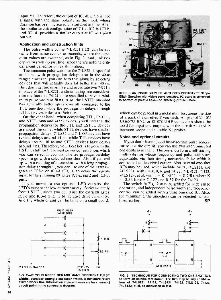
input Yl. Therefore, the output of IC 1-b, pin 6 will be a signal with the same polarity as the input, whose duration has been increased or stretched in time. Also, the similar circuit configuration of IC 1-c, IC2-b, IC3-b, and ICI -d, provides a similar output at ICI-d's pin 8 output.
Application and construction hints The pulse widths of the 74LS221 (IC2) can be any
value from nanoseconds to seconds, where the capa- citor values are switched, as in Fig. 2. And junk box capacitors will do just fine, since there's nothing criti- cal about capacitor or resistor values.
The minimum pulse width for the 74LS221 is specified at 40 ns, with propagation delays also in the 40-ns range; however, you can help that along by selecting devices that will actually do a lot better than 40 ns. But, don't get too inventive and substitute two 7412l's in place of the 74LS22I, without taking into considera- tion the fact that 74121's are specified to have a mini- mum pulse width at 50 ns. Also, the LSTTL one-shot has generally better specs over all, compared to the TTL one-shot, while the propagation delays through LTTL devices rules out their use.
On the other hand, when comparing TTL, LSTTL, and STTL 7486 and 7432 devices, you'll find that the propagation delays for the TTL and LSTTL devices are about the same, while STTL devices have smaller propagation delays. 74LS32 and 74LS86 devices have typical delays around 14 ns, while TTL devices have delays around 10 ns and STTL devices have delays around 7 ns. Therefore, your best bet is to go with the LSTTL stuff for the lowest power consumption, which you can select if you want better propagation -delay specs to go with a selected one-shot. Also, if you end up with a real dog of a one-shot, with a long propaga- tion delay throught it, you can use one of the extra OR gates in IC3-c or 1C3 -d (Fig. 1) to delay the signals input to the summing oR gates IC3-a, pin 2 and IC3-b, pin 5.
If you intend to use optional LED outputs, the LED's must be the low -current variety, if driven directly from LSTTL, albeit you could use the extra OR gates IC3-c and IC3-d (Fig. 1) to increase drive capability. And the whole circuit can be built on a small board,
PULSE WIDTH CAPACITORS
o
o
o
o
o
IC2 PIN 14, (IC2 PIN 5) IC2 PIN 15
(IC2 PIN 7)
FIG. 2-IF YOUR NEEDS DEMAND MANY DIFFERENT PULSE widths, consider adding a capacitor switch. A miniature rotary switch works fine. Information in parentheses are for channel -2 circuit point in the schematic diagram.
R1 (R3)
R2 11341
+5V
JI R6 R5 IC1 C2
R4
BATTERY HOLDER
BAIT 1
HERE'S AN INSIDE VIEW OF AUTHOR'S PROTOTYPE Scope Glitch Stretcher with visible parts identified. PC board is cemented to bottom of plastic case-no shorting problem here.
which can be placed in a metal mini -box about the size of a pack of cigarettes if you wish. Amphenol 31-102/ UG657U BNC or 83-878 UHF connectors should be used for input and output, with the circuit plugged in between scope and suitable X1 probes.
Notes and optional circuits If you don't have a good fast -rise -time pulse genera-
tor to test the circuit, you can use two interconnected one -shots as in Fig. 3. The one -shots form a self-starting multi -vibrator whose frequency and pulse width are adjustable, via their timing networks. Pulse width is controlled as described earlier. Also, several one-shot IC's may be used, which include 74121, 74LS121, and 74LS221, with t = 0.7CR and 74122, 74LS122, 74123, 74LS123, et al, with t = K RC (1 + 0.7/R), where K = 0.32 for the 74122 and 0.37 for the 74123.
The switch in Fig. 2 may be added for wide range operation, and independent pulse width and frequency control can be added with a third one-shot IC. Also, for minimum t, the one -shots can be selected, as out- lined earlier. SP
+5V A
C
+5V A
R C
K
J L A Q A Q
r' LJ LJ
r-- B Q B Q
ALTERNATE _J
FIG. 3-TECHNIQUE FOR CONNECTING TWO ONE-SHOT IC'S to form an astable test circuit. The IC's may be any combina- tion of 74LS221, 74121, 74LS121, 74122, 74LS122, 74123, 74LS123, et al, as discussed in text.

Ìi 8=ar. A t .ts^st ZaLsStXseS úliYie
Turing i,t v1stdtin.e sJ Step-by-step .a7 ír;ïQ%
Radio Elecironu
COMPLETE
AV {Or
the F RST T1110.1
r r y i z;,. MAN r r r r 4' l ,aói: J.'s... i .64i ÿS2 i:éG;: :f. LúG «7iies:LE
$1.25 AU CZ. VAC
BUILD YOUR OWN ROBOT! Send today for your 52 -page (81/2 x
11") booklet containing complete re-
prints of all eleven articles in the Build Your Own Robot series by Jim Gupton.
This all-inclusive reprint gives you all
the data you need to build your own Robot.
TELLS EVERYTHING YOU NEED TO KNOW to build the Unicorn -1
Robot without the need for an engi- neering degree or special equipment.
The robot is fully mobile with minipu- lator arms to grasp, lift and carry.
MANIPULATOR ARMS and end - effectors (hands) are what enable the robot to perform useful tasks. Details of construction techniques and con- siderations are fully explored.
MOBILITY BASE is not a lunar space station. It is the drive system that permits the robot to move from here to there. Full construction de- tails along with a discussion of power sources is included.
THE BODY-FRAME AND ROTA-
TION MECHANISM. This is the part that makes Unicorn -1 look like a ro-
bot. Wood and Formica are the ma-
terials for the body. Motors and gears are what make it function.
COMMUNICATIONS. How you can tell your robot what to do. Prepro- gramming techniques....radio control ....computer control are all detailed.
SENSORS. How to add sensors so
your robot doesn't bump into things.
Radio - Electronics
Robot Reprints 200 Park Ave. South New York, N.Y. 10003
I want to order reprints @$12.00 plus $1.00 postage and handling for U.S., Canada and Mexico. Add 96c sales tax for New York State residents only. U.S. Funds only. I want to order reprints @$12.00 plus $3.00 Air Postage and handling for all other countries. U.S. Funds only.
Allow 6-8 weeks for delivery.
Please print
(Name)
(Street address)
(City) (State)
We do not bill, check must be enclosed.
SPF1
WIRELESS CW KEYING MONITOR
continued from page 81
Final assembly First install all the cabinet components, including BPI.
Then secure the PC board to the cabinet with a single mount- ing screw,' using a metal standoff (often called a "spacer") between the cabinet and the board. Any size standoff can be used, as long as it lifts the board above the binding post. If you don't have a standoff, use a long screw and a stack of washers or nuts as a substitute for a spacer. The ground connection to the cabinet is through the standoff, so make certain you have a solid contact between it and the foil around the mounting hole. Insure a good electrical ground by using an internal lockwasher between the standoff and the PC board.
Checkout Set power switch S 1 OFF, install a battery, and set S1 on.
Ground the negative end of the battery holder to the cabinet. If that doesn't produce a tone, either you have made a wiring error, or Q3 or Q4 is defective.
Using the monitor Position the monitor on your desk, preferably near the
transmitter, and connect a 12 -inch length of stiff wire-such as a cut -down wire coat hanger-to BP1. Turn on the transmitter and the keying monitor, and then key the transmitter. You should hear a tone when the key is down. Adjust R3 to change the pitch (frequency) of the tone.
If keying the rig doesn't produce a tone, connect a length of insulated wire to the binding post and wrap a few turns of
11111111111111111111111111F THOUGH THE WIRELESS CW KEYING MONITOR is powered by an internal battery, the trigger signal for the oscillator is a minute sample of the RF energy radiated by the transmitter antenna. There is no direct connection between the transmitter or antenna system and the monitor.
the free end around the transmission line. If that also doesn't produce a tone, slip a few inches of the insulated wire through a ventilation opening into the transceiver near the RF final stage. SP
BEAT -FREQUENCY OSCILLATOR Continued from page 43
caused by improper installation of the coaxial plugs. If the circuit is oscillating, go back and make sure you have coupled the BFO signal to the proper lead of the proper stage in the CB.
If everything is working properly, turn the BFO off (S 1 to the AM position) and re -connect the antenna to the CB. Turn the CB on and listen to the upper channels starting at 40 and proceeding downward, until you hear a SSB transmission. It will be recognized as a garbled noise, with the S -meter rising and falling in accordance with the strength of the noise. Turn the BFO on, and carefully adjust T I until you can recognize a voice close to normal pitch. If the signal is very strong, you may need to throw S1 to the STRONG position. C3 can now be used to fine tune for natural voice quality. Adjust T l so that C3 tunes to the center of the channel with its plates half -meshed. Thereafter, TI should not require any fur- ther adjustment. Using C3, you will be able to separate one station from another on the same channel.
Since not all CB transceivers are identical, the BFO signal strength may varyfrom its optimum value. With S2 in the "weak" position, the BFO should cause the S -meter to hold steady at "S2" or "S3", with no signal being received or the antenna disconnected. In the STRONG position, the meter should read about "S7". Any significant departure from these readings can be reme- died by varying values of C4 and C5. SP
reeri 77-91; PRINTED CIRCUIT KIT Makes circuits THREE WAYS
1 FULL SCALE ARTWORK MASTER
3 DIRECT ETCH DRY TRANSPIRE APPLIED TO COPPER C
Copy circuits right from a magazine using special photo film. No camera or darkroom used. Page is not destroyed in process. Do your own master art, make negatives, sensitize boards and etch one or a hundred circuits; all identical, all perfect. For one -of -a -kind PC's, use special dry transfer patterns as a direct etch resist right on the blank copper board. Do it all with the ER -4. In stock at parts distributors or order direct. Add 7% shipping. Minimum factory order: $30.00.
ER -4 Complete Photo Etch Set $34.95 ER -2 Assorted Etch Resist Patterns & Tapes 5.50 ER -3 1/4 lb. Dry Ferric Chloride (makes one pint) 2.50 ER -5 Six sheets Pos-Neg Copy Film, 5"x6" 5.50 ER -6 Film Process Chemicals 2.95 ER -71 Photo Resist Liquid (negative) does 1700 in2 6.95 ER -8 Photo Resist Developer, 16 oz. 3.95 ER -18 Tinnit® Bright Tin Plate 3.50
DEVELOPED
2 ILLUSTRATION POSITIVE NEGATIVE lefr COPPER GCLADPHOTO
RESIST
ARD CIRCUI CIRCUIT BOARD
LAD BOARD
the DATAK corn. 65 71st St. Guttenberg. N. J. 07093
94 CIRCLE 605 ON READER SERVICE CARD
DUAL VOLTAGE POWER SUPPLY
continued from page 77
and polarity, using the layout chart as a guide. Pay particular attention to the proper installation of diodes D1 and D2 as well as IC1 and IC2. A mistake here could cause instant destruction of parts if incorrectly installed. If the power should fail to operate when plugged into the 120 VAC outlet, normal service checks should include being certain that the power cord is properly connected to the transformer's pri- mary winding printed circuit tabs and that the secondary winding of T1 is connected to the circuit foils. A voltmeter will quickly confirm the presence of 12.6 VAC at the secon- dary terminals telling the builder that the problem is follow- ing the power transformer in the circuit. If LED1 glows properly, it also is a good indication that the transformer and D2 are operating correctly.
Once you have passed the "smoke test" area, but the supply still has no output voltage from one or both suppliers, your best action would be to recheck your wiring and solder- ing to be certain that the parts are installed in their proper locations and with the polarities indicated on the schematic diagram (Fig. 1) and component layout diagram (Fig. 3). Bear in mind that if you should find one of the diode rectifi- ers, or IC regulators, improperly installed, there is a fifty- fifty chance that it may be damaged.
Another possible trouble symptom could be the refusal of the output voltage to adjust in response to the voltage adjust control which will indicate a poorly soldered joins at one or more of the reference -voltage -resistance -divider chain. In practice, since the output voltage from the IC is applied across (for example) the series -connected R2 and R3 network (see Fig. 1), it will follow any up and down excursions which the load may tend to cause at the output. A portion of this, voltage change is tapped off by the variable resistor (R3) and
returned as a reference voltage to be used by the IC which in turn either lowers or raises the output voltage. The net effect is to maintain a very stable output voltage. Therefore, as can be anticipated, a loose connection, short, or other defect in this reference circuit will cause a problem with the adjust- ment of the voltage as well. Defective or incorrectly installed electrolytic capacitors C3 and C4 will make the supply di- fficult to adjust and if the output voltage varies or drops under load, improper values of Cl and C2 may be suspected.
It is important to understand that the positive and negative supplies share a common ground connection. If the supply is used for two projects at one time, each supply may be called upon to provide the single polarity needed. For instance, two isolated units may be operated using 5 volts to each. One unit may be used in the normal manner across the positive supply while the second unit under test can be operated by the negative supply by merely reversing the leads at the supply ...positive lead to the ground terminal of the power supply and the negative (common ground) to the negative terminal of the power supply. It will not require much thought to realize that there can be no common ground connection between these two units under test since it would amount to a short across the output terminals of the power supply.
If the power supply is to be housed in a case or other enclosed area, be sure to consider the temperature rise that could occur unless proper ventilation is supplied. No fuse or on/off switch is provided on the power supply board. Such items may be inserted into the circuit by removal of jumper (JW1) and soldering their leads to these board terminals.
The low cost of construction of the Dual Variable Power Supply will provide a very valuable investment for your electronics experimenting and building projects by the con- venience offered through the usefulness of having on hand a dual polarity, adjustable, and regulated power supply. SP
Ever reflect on a career
inthe Nuclear Navy?
Take a good look at yourself. Your life. You've worked hard to get where you are. But where are you going from here?
Today's Navy can turn your scientific or engineering studies into a nuclear specialty that will make you a than you ever thought you could go.
From a cruiser loaded with the latest electronic equipment, to a giant nuclear carrier, you'll get valuable technical training in the Navy. Plus good pay, travel, free dental and medical care and 30 days' vacation with pay, your very first year. Not to mention more experiences than you'd get in a lifetime on land.
Interested? Take a closer look at today's Nuclear Navy. Motivated? Then today's Navy would eke to have a look at you. Because people like you are a
good reflection on us.
part of a professional team. And it may
Call toll -free: 800.841-8000 (in Georgia, 800.342-5855).
NAVY. IT'S NOT JUST A JOB, IT'S AN ADVENTURE.
take you farther
LOCK-OUT
continued from page 70
each hand) at the same times and light two LED's. Yet, it is possible for an eight -way tie to be sensed by Lock -Out. That can be proven by connecting two or more inputs together and then pressing a button. Normally, ties will occur when two or more buttons are depressed within 40 to 80 nanoseconds of each other.
Final touches Sensing switches can be fabricated in the manner used in
the model by simply inserting small pushbutton switches into the end of small diameter tubing or heat -shrink tubing. The latter can be shrunk around the switch body for a tight fit. The game action buttons are made by the heat -shrink tubing method. Each switch is at the end of a two-inch piece of tubing, which feels quite comfortable in the hand and is easy to use.
Construct a copy of Lock -Out and take it to your next party, just to see who has the fastest reaction time to some action. Who knows-perhaps, by installing a microswitch, or some other sensing unit to the tracks of a slot -car or soap -box derby race, it will be much easier to tell which car came in first.
Of course, this unit will show only the winner ...but it can be modified so as to indicate win, place, and show. Howev- er, that's another project, perhaps. SP
F>
G >
S2
RESET
LED 8 7 6 5 4
SPEAKER 3 2 LEDI
®®®0 ® 00
H A
EU U B
Y Y
-R5-
165
IC3
D * 11
R2
I 0.1 I
R4 R3 I
'C1
ICI
IC2
<C
<D
+
OFF
B1
T
R1
FIG. 6-LOCATION OF COMPONENT PARTS on the printed - circuit board. Ghosted copper foil is shown face down. If a perfboard is used, select a board with .1 -inch hole centers, and locate the components as if they were on the printed -circuit board as shown above. Then, either hard solder or wire -wrap the circuit. Be sure to use different colored insulated wires.
Do with
your A P
breadboarding PRODUCTS new
by the numbers TM
soldering...when
them #22AWGsolidhook
Now
projects. boards...no
electronic A P
Circuit-Strips?M With
all plug and
there's an easy way to build your electronic
No need for perf need for
you build circuits with
PRODUCTS new
Circuit -Strips, you do is simply
in components :. interconnect with ordinary :':
solderless Circuit -Strips are compatible with DIP's of all sizes and a wide variety of dis- crete components which can be used over and over again.
Circuit -Strips have a
`:'::.: ' -
i :' .. " ' ` '
a .,: ` `
feature 610 plug-in tie -points, and have a capacity of up to 6 14 -pin DIP's. Model #923253 is available with
alloy 770 terminals at only $14. Model #923749 is
available with gold plated alloy 770 terminals at
- - - - only$28.
' Call TOLL FREE, 800321-9668, - . - . for the name of `' -
up wire. Circuit- .
Strips' spring clip .. terminals not only ,.... accommodate a wide range of
% . : r - -
.. ... .. . -. . ..,.. ... . .,, the distributor + :: nearest you. (In Ohio,
r p calloolleot. .. (216) 354-2101.)
leads, but also provide excellent electrical connection to every one.
Economically
molded -in alpha -numeric grid for faster and easier Identification of every tie-
in They
A P PRODUCTS INCORPORATED 9450 Pineneedle Drive
Mentor Box 603 [216] 354-2101
TWX: 810-425-2250 priced, point your circuit. In Europe, contact A P PRODUCTS GmbH
Baeumlesweg 21 D-7031 Weil 1 W. Germany
CIRCLE 604 ON READER SERVICE CARD
OPTO POWER SWITCH
continued from page 62
component. Now apply your DC control voltage to J1 . The lamp should light. If it doesn't, connect a DC milliammeter in series with one of the wires to J 1 and note the current. If it is zero, check your connections and the installation of BR 1- AFTER PULLING THE POWER CORD (don't depend on Si). If the meter reads between 12 and 20 -mA, check for a
THE AC-POWERLINE WIRES PASS THROUGH A NOTCH cut into the end of the cabinet. They are secured when the cabinet cover is in place.
THE WIRES TO CONTROL JACK J1 ARE ON THE FOIL SIDE of the PC board. They are tack -soldered to the foil pads.
wiring error from ICI's output through to SOI. If you are using an AC control voltage make certain it
provides 12 to 20 DCmA to the LED in ICI. You must connect the meter in series with the diode. If you use the PC construction, the easiest place to make the measurement is in series with resistor R. SP
DISCO LIGHT ORGAN CONTROL continued from page 21
PARTS LIST RESISTORS
Resistors '/2 watt, 10% unless otherwise noted R1-180,000 ohms R2-100,000 ohms R3-1000 ohms R4-4700 ohms, 2 watts R5 -R8-10,000 ohms R9-22,000 ohms R10 -R12-10.000 ohms, linear -taper potentiometer CAPACITORS
Cl, C2 -5-µF, 25 volts electrolytic C3 -25-µF, 25 volts electrolytic C4, C6 -0.001-1F, 24 volts ceramic disk C5 -0.022-µF, 200 -volts (Sprague Orange Drop type-
225P22392XD3) C7 -0.29,F, 200 volts (Sprague Orange Drop type-
225P22492XD3) SEMICONDUCTORS
01-1 N5223 transistor D1, D2, D3-IN2069, 1 amp, 200 -Ply silicon SCR1, SCR2, SCR3-4 amp, 200-PIV (see text) MISCELLANEOUS
T1-Audio transformer, 2000 -ohms primary winding to 10,000 -ohms secondary winding
S1-SPST 15 -amp, 125 -VAC toggle switch NE1-NE4-neon lamps, 117 -VAC chassis mount with built-in,
current -limiting resistors SO1, SO2, S03-AC sockets, chassis mount J1-Phono jack F1-15 amp fuse with panel -mount holder AC line cord, steel box or cabinet, hardware, knobs, solder,
black paint or covering material, etc.
Should you expect to move the unit to various locations for party disco activities, use a steel box (suggested in the Parts List). Otherwise, an aluminum box for permanent in- stallations is sufficient. The author ommitted fuse FI shown in the schematic diagram. which we suggest be included in
your device. If a three -prong power plug is used, connect the green lead to case ground. Also, use three -prong sockets and connect the green -screw terminal to the same bolt on case ground that the line cord green lead uses.
The entire Disco Light Organ Control circuit can be built for less than 530 and will add a new sense of life and entertainment to your music atmosphere. Go ahead; build your own Disco Light Organ Control and have your whole room dancing to music! SP
St MASTER
RIO M10SAMGE
all LOW M12
HERE'S THE AUTHOR'S MODEL covered with a textured materi- al. The effect is cosmetic, and offers very little rough handling protection. The black color for the unit is in keeping with audio reinforcement products of this type found in the field.
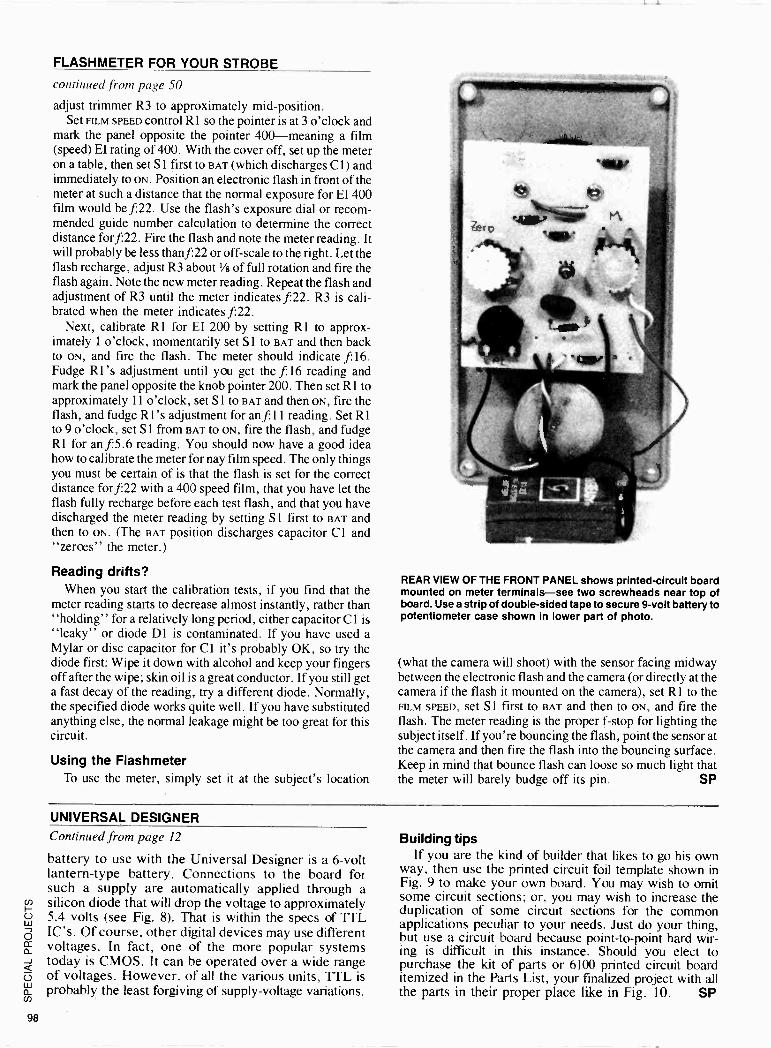
FLASHMETER FOR YOUR STROBE
continued from page 50
adjust trimmer R3 to approximately mid -position. Set FILM SPEED control R1 so the pointer is at 3 o'clock and
mark the panel opposite the pointer 400-meaning a film (speed) EI rating of 400. With the cover off, set up the meter on a table, then set S1 first to BAT (which discharges C1) and immediately to ON. Position an electronic flash in front of the meter at such a distance that the normal exposure for EI 400 film would be f:22. Use the flash's exposure dial or recom- mended guide number calculation to determine the correct distance for f:22. Fire the flash and note the meter reading. It will probably be less than f..22 or off -scale to the right. Let the flash recharge, adjust R3 about Vs of full rotation and fire the flash again. Note the new meter reading. Repeat the flash and adjustment of R3 until the meter indicates f:22. R3 is cali- brated when the meter indicates f:22.
Next, calibrate R1 for EI 200 by setting RI to approx- imately 1 o'clock, momentarily set S1 to BAT and then back to ON, and fire the flash. The meter should indicate f:16. Fudge R1 's adjustment until you get the f:16 reading and mark the panel opposite the knob pointer 200. Then set R1 to approximately 11 o'clock, set S 1 to BAT and then ON, fire the flash, and fudge Rl's adjustment for an f:11 reading. Set R1 to 9 o'clock, set S1 from BAT to ON, fire the flash, and fudge R1 for an f:5.6 reading. You should now have a good idea how to calibrate the meter for nay film speed. The only things you must be certain of is that the flash is set for the correct distance fort 22 with a 400 speed film, that you have let the flash fully recharge before each test flash, and that you have discharged the meter reading by setting Si first to BAT and then to ON. (The BAT position discharges capacitor Cl and "zeroes" the meter.)
Reading drifts? When you start the calibration tests, if you find that the
meter reading starts to decrease almost instantly, rather than "holding" for a relatively long period, either capacitor Cl is "leaky" or diode D1 is contaminated. If you have used a Mylar or disc capacitor for Cl it's probably OK, so try the diode first: Wipe it down with alcohol and keep your fingers off after the wipe; skin oil is a great conductor. If you still get a fast decay of the reading, try a different diode. Normally, the specified diode works quite well. If you have substituted anything else, the normal leakage might be too great for this circuit.
Using the Flashmeter To use the meter, simply set it at the subject's location
REAR VIEW OF THE FRONT PANEL shows printed -circuit board mounted on meter terminals-see two screwheads near top of board. Use a strip of double -sided tape to secure 9 -volt battery to potentiometer case shown in lower part of photo.
(what the camera will shoot) with the sensor facing midway between the electronic flash and the camera (or directly at the camera if the flash it mounted on the camera), set R1 to the FILM SPEED, set S1 first to BAT and then to ON, and fire the flash. The meter reading is the proper f-stop for lighting the subject itself. If you're bouncing the flash, point the sensor at the camera and then fire the flash into the bouncing surface. Keep in mind that bounce flash can loose so much light that the meter will barely budge off its pin. SP
UNIVERSAL DESIGNER Continued from page 12
battery to use with the Universal Designer is a 6 -volt lantern -type battery. Connections to the board for such a supply are automatically applied through a silicon diode that will drop the voltage to approximately 5.4 volts (see Fig. 8). That is within the specs of TTL IC's. Of course, other digital devices may use different voltages. In fact, one of the more popular systems today is CMOS. It can be operated over a wide range of voltages. However, of all the various units, TTL is probably the least forgiving of supply -voltage variations.
Building tips If you are the kind of builder that likes to go his own
way, then use the printed circuit foil template shown in Fig. 9 to make your own board. You may wish to omit some circuit sections; or, you may wish to increase the duplication of some circuit sections for the common applications peculiar to your needs. Just do your thing, but use a circuit board because point-to-point hard wir- ing is difficult in this instance. Should you elect to purchase the kit of parts or 6100 printed circuit board itemized in the Parts List, your finalized project with all the parts in their proper place like in Fig. 10. SP
98
Get it all! Subscribe today to RADIO -ELECTRONICS. Don't miss a single issue and ... you save as much as $11.28 off the newsstand price. When you select one of the subscription offers listed on the handy coupon-you'll be assured of having your copy reserved, even if it sells out on the newsstand. Make sure you get all the excitement in every issue of RADIO -ELECTRONICS, every month, by filling in and mailing the coupon, today.
This will be coming to you when you subscribe to RADIO -ELECTRONICS:
HELPFUL CONSTRUCTION ARTICLES ...
Test Equipment Hi-Fi Accessories Telephone Accessories Music Synthesizers Computer Equipment Automotive Equipment Intruder Alarms- Home & Car
Radio Electronics.
NEWS ON NEW TECHNOLOGY ...
Android Design (Robots That Think and Do) Automotive Electronics Speech Synthesizers IC Applications Video Disc Players Video Tape Recorders
SAVE MONEY, enclose your payment and you get ONE EXTRA ISSUE. FOR NEW SUBSCRIBERS ONLY.
FASCINATING "HOW TO DO IT" ARTICLES ...
Build Your Own Projects Make Your Own PC Boas ds Wiring Techniques Soldering and Desoldering Design and Prototyping
L
HOW YOU AND THE COMPUTER CAN BE FRIENDS ...
Getting Started Programs, Circuit Design, Games A/D-D/A Interfacing Peripheral Equipment
NEW AUDIO DIMENSIONS FOR YOUR PLEASURE ...
Noise -Reduction Devices Correct Bias for Your Tape Deck How to Connect that Extra Add -On Monthly Features by Len Feldman
Radio- Electronics
TV WONDERS FOR YOUR FUTURE ...
Latest Receivers and Circuits Projection TV Today Satellite TV Receivers Jack Darr's Monthly Service Clinic Service Problems and Solutions
AND you also get these regular MONTHLY FEATURES:
LOOKING AHEAD by Dave Lachenbruch HOBBY CORNER by "Doc" Savage
WHAT'S NEWS, new products, stereo news
and NEW IDEAS, STEREO PRODUCTS, NEW COMPUTER PRODUCTS FOR HOME/JOB and MUCH MORE!
YES! please send me Payment enclosed, 13 issues for $10.97
(You save $5.28 off newsstand price.)
Payment enclosed, 25 issues for $19.97 (Save More! $11.28 off newsstand price.)
Bill me, 1 year -12 issues only $10.97 (You save $4.03 off newsstand price.)
Bill me, 2 years -24 issues only $19.97 (Save more! $10.03 off newsstand price.)
Extra postage: Canada $3.00 per year. All other countries $7.50 per year.
Name
Address
City State
7S520
Every Month! Get the Best - Clip Coupon - Mail Today!
U.S. Funds Only
(please pnnt)
Mail to: RADIO -ELECTRONICS PO. Box 2520, Boulder, Colorado 80322
Zip Code
Allow 6-8 weeks for delivery of first issue.
J
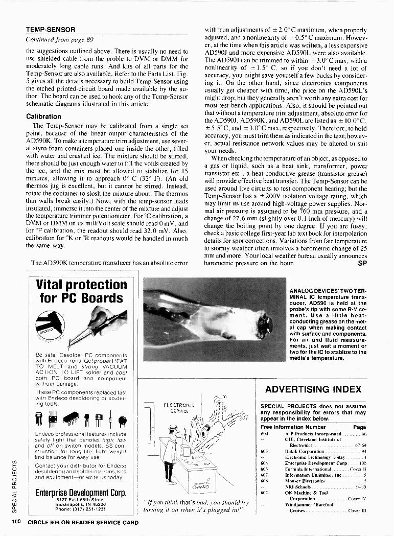
I
TEMP -SENSOR
Continued from page 89
the suggestions outlined above. There is usually no need to use shielded cable from the proble to DVM or DMM for moderately long cable runs. And kits of all parts for the Temp -Sensor are also available. Refer to the Parts List. Fig. 5 gives all the details necessary to build Temp -Sensor using the etched printed -circuit board made available by the au- thor. The board can be used to hook any of the Temp -Sensor schematic diagrams illustrated in this article.
Calibration The Temp -Sensor may be calibrated from a single set
point, because of the linear output characteristics of the AD590K. To make a temperature trim adjustment, use sever- al styro-foam containers placed one inside the other, filled with water and crushed ice. The mixture should be stirred, there should be just enough water to fill the voids created by the ice, and the mix must be allowed to stabilize for 15 minutes, allowing it to approach 0° C (32° F). (An old thermos jug is excellent, but it cannot be stirred. Instead, rotate the container to slosh the mixture about. The thermos thin walls break easily.) Now, with the temp -sensor leads insulated, immerse it into the center of the mixture and adjust the temperature trimmer potentiometer. For °C calibration, a DV.M or DMM on its milliVolt scale should read 0 mV, and for °F calibration, the readout should read 32.0 mV. Also, calibration for °K or °R readouts would be handled in much the same way.
The AD590K temperature transducer has an absolute error
Vital protection for PC Boards
Be safe. Desolder PC components with Endeco irons. Get proper HEAT TO MELT and strong VACUUM ACTION TO LIFT solder and cool both PC board and component without damage.
These PC components replaced fast with Endeco desoldering or solder- ing tools.
re -He Endeco professional features include safety light that denotes high, low and off on switch models, SS con- struction for long life, light weight 'and balance for easy use.
Contact your distributor for Endeco desoldering and soldering irons, kits and equipment-or write us today.
Enterprise Development Corp. 5127 East 65th Street Indianapolis, IN 46220 Phone: (317) 251-1231
with trim adjustments of ± 2.0° C maximum, when properly adjusted, and a nonlinearity of ± 0.5° C maximum. Howev- er, at the time when this article was written, a less expensive AD590J and more expensive AD590L were also available. The AD590J can be trimmed to within ± 3.0° C max, with a nonlinearity of ± 1.5° C, so if you don't need a lot of accuracy, you might save yourself a few bucks by consider- ing it. On the other hand, since electronics components usually get cheaper with time, the price on the AD590L's might drop; but they generally aren't worth any extra cost for most test -bench applications. Also, it should be pointed out that without a temperature trim adjustment, absolute error for the AD590J, AD590K, and AD590L are listed as ± 10.0°C, ± 5.5° C, and ± 3.0° C max, respectively. Therefore, to hold accuracy, you must trim them as indicated in the text; howev- er, actual resistance network values may be altered to suit your needs.
When checking the temperature of an object, as opposed to a gas or liquid, such as a heat sink, transformer, power transistor etc., a heat -conductive grease (transistor grease) will provide effective heat transfer. The Temp -Sensor can be used around live circuits to test component heating; but the Temp -Sensor has a ± 200V isolation voltage rating, which may limit its use around high -voltage power supplies. Nor- mal air pressure is assumed to be 760 mm pressure, and a change of 27.6 mm (slightly over 0.1 inch of mercury) will change the boiling point by one degree. If you are fussy, check a basic college first -year lab text book for interpolation details for spot corrections. Variations from fair temperature to stormy weather often involves a barometric change of 25 mm and more. Your local weather bureau usually announces barometric pressure on the hour. SP
ANALOG DEVICES' TWO TER- MINAL IC temperature trans- ducer, AD590 is held at the probe's tip with some R-V ce- ment. Use a little heat - conducting grease on the met- al cap when making contact with surface and components. For air and fluid measure- ments, just wait a moment or two for the IC to stablize to the media's temperature.
ELECTRONIC SERVIcE
"If you think that's bad, you should try turning it on when it's plugged in!"
ADVERTISING INDEX
SPECIAL PROJECTS does not assume any responsibility for errors that may appear in the index below.
Free Information Number Page 604 A P Products Incorporated 96
CIE, Cleveland Institute of Electronics 67-69
605 Datak Corporation 94 Electronic Technology Today 4
606 Enterprise Development Corp 100
603 Formula International Cover II
607 Information Unlimited, Inc 5
608 Mouser Electronics 5
NRI Schools 34-35 602 OK Machine & Tool
Corporation Cover IV
Windjammer `Barefoot' Cruises Cover III
CIRCLE 606 ON READER SERVICE CARD

...you should seethe rest! It's full of fun, sun, barefeet & bikinis. It's runnin' with the wind to small, tropical islands and unique ports o' call for those with itchy feet and adventure in their soul.
We're not the Love Boat, but we'll take on anybody when it comes to beach- combing, sailing & exploring the exotic Carib- bean. It's our backyard and we know all the great places in paradise. And, 6 -day cruises start from $425.
So send for the rest of the booklet. It's free!
Look us over & "sea it" our way!
Cruises, LTD.
Box 120, Dept , Miami Beach, FL 33119-0120 or call TOLL FREE and tell us you need the rest of the booklet: 800-327-2600 in FL: 800-432-3364
Got a Problem? with integrated circuits
Answer WK8 Troubleshooter Kit PRB-1 Digital Logic Probe PLS-1 Logic Pulser
EX -1 DIP IC Extractor Tool EX -2 CMOS Safe DIP IC Extractor Tool MOS-1416 14-16 Pin MOS/CMOS Safe Inserter MOS-2428 24-28 Pin MOS/CMOS Safe Inserter MOS-40 36-40 Pin MOS/CMOS Safe Inserter
WRS-1 Wrist Strap
OH Machine & Tool Corporation 3455 Conner St., Bronx, N.Y. 10475 U.S.A.
Tel.(212) 994-6600 Telex 125091
CIRCLE 202 ON READER SERVICE CARD