Embed Size (px)
Citation preview
May 2007 Rev 3 1/22
1
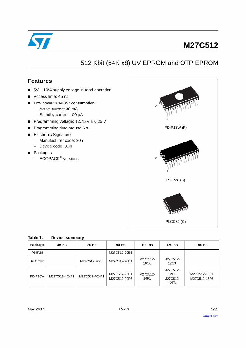
M27C512
512 Kbit (64K x8) UV EPROM and OTP EPROM
Features 5V ± 10% supply voltage in read operation
Access time: 45 ns
Low power “CMOS” consumption:– Active current 30 mA– Standby current 100 µA
Programming voltage: 12.75 V ± 0.25 V
Programming time around 6 s.
Electronic Signature– Manufacturer code: 20h– Device code: 3Dh
Packages– ECOPACK® versions
1
28
28
1
FDIP28W (F)
PDIP28 (B)
PLCC32 (C)
Table 1. Device summary
Package 45 ns 70 ns 90 ns 100 ns 120 ns 150 ns
PDIP28 M27C512-90B6
PLCC32 M27C512-70C6 M27C512-90C1M27C512-
10C6M27C512-
12C3
FDIP28W M27C512-45XF1 M27C512-70XF1M27C512-90F1M27C512-90F6
M27C512-10F1
M27C512-12F1
M27C512-12F3
M27C512-15F1M27C512-15F6
www.st.com
Contents M27C512
2/22
Contents
1 Description . . . . . . . . . . . . . . . . . . . . . . . . . . . . . . . . . . . . . . . . . . . . . . . . . 3
2 Device operation . . . . . . . . . . . . . . . . . . . . . . . . . . . . . . . . . . . . . . . . . . . . 5
2.1 Read mode . . . . . . . . . . . . . . . . . . . . . . . . . . . . . . . . . . . . . . . . . . . . . . . . . 5
2.2 Standby mode . . . . . . . . . . . . . . . . . . . . . . . . . . . . . . . . . . . . . . . . . . . . . . 5
2.3 Two line output control . . . . . . . . . . . . . . . . . . . . . . . . . . . . . . . . . . . . . . . . 6
2.4 System considerations . . . . . . . . . . . . . . . . . . . . . . . . . . . . . . . . . . . . . . . . 6
2.5 Programming . . . . . . . . . . . . . . . . . . . . . . . . . . . . . . . . . . . . . . . . . . . . . . . 7
2.6 PRESTO IIB programming algorithm . . . . . . . . . . . . . . . . . . . . . . . . . . . . . 7
2.7 Program Inhibit . . . . . . . . . . . . . . . . . . . . . . . . . . . . . . . . . . . . . . . . . . . . . . 8
2.8 Program Verify . . . . . . . . . . . . . . . . . . . . . . . . . . . . . . . . . . . . . . . . . . . . . . 8
2.9 Electronic Signature . . . . . . . . . . . . . . . . . . . . . . . . . . . . . . . . . . . . . . . . . . 8
3 Erasure operation (applies for UV EPROM) . . . . . . . . . . . . . . . . . . . . . . 9
4 Maximum rating . . . . . . . . . . . . . . . . . . . . . . . . . . . . . . . . . . . . . . . . . . . . 10
5 DC and AC parameters . . . . . . . . . . . . . . . . . . . . . . . . . . . . . . . . . . . . . . 11
6 Package mechanical . . . . . . . . . . . . . . . . . . . . . . . . . . . . . . . . . . . . . . . . 17
7 Part numbering . . . . . . . . . . . . . . . . . . . . . . . . . . . . . . . . . . . . . . . . . . . . 20
8 Revision history . . . . . . . . . . . . . . . . . . . . . . . . . . . . . . . . . . . . . . . . . . . 21
M27C512 Description
3/22
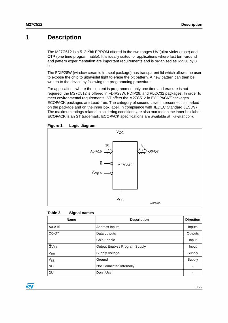
1 Description
The M27C512 is a 512 Kbit EPROM offered in the two ranges UV (ultra violet erase) and OTP (one time programmable). It is ideally suited for applications where fast turn-around and pattern experimentation are important requirements and is organized as 65536 by 8 bits.
The FDIP28W (window ceramic frit-seal package) has transparent lid which allows the user to expose the chip to ultraviolet light to erase the bit pattern. A new pattern can then be written to the device by following the programming procedure.
For applications where the content is programmed only one time and erasure is not required, the M27C512 is offered in FDIP28W, PDIP28, and PLCC32 packages. In order to meet environmental requirements, ST offers the M27C512 in ECOPACK® packages. ECOPACK packages are Lead-free. The category of second Level Interconnect is marked on the package and on the inner box label, in compliance with JEDEC Standard JESD97. The maximum ratings related to soldering conditions are also marked on the inner box label. ECOPACK is an ST trademark. ECOPACK specifications are available at: www.st.com.
Figure 1. Logic diagram
Table 2. Signal names
Name Description Direction
A0-A15 Address Inputs Inputs
Q0-Q7 Data outputs Outputs
E Chip Enable Input
GVPP Output Enable / Program Supply Input
VCC Supply Voltage Supply
VSS Ground Supply
NC Not Connected Internally -
DU Don’t Use -
AI00761B
16
Q0-Q7
VCC
M27C512
GVPP
VSS
8
A0-A15
E
Description M27C512
4/22
Figure 2. DIP connections
Figure 3. LCC connections
A1A0Q0
A7
A4A3A2
A6A5
A13
A10
A8A9
Q7
A14
A11GVPP
E
Q5Q1Q2
Q3VSS
Q4
Q6
A12A15 VCC
AI00762
M27C5128
1234567
91011121314
1615
282726252423222120191817
AI00763
A13
A8
A10
Q4
17
A0NCQ0
Q1
Q2
DU
Q3
A6
A3A2A1
A5A4
9
A14
A9
1
A15
A11
Q6
A7
Q7
32
DU
VC
C
M27C512
A12
NC
Q5
GVPP
E
25
VS
S
M27C512 Device operation
5/22
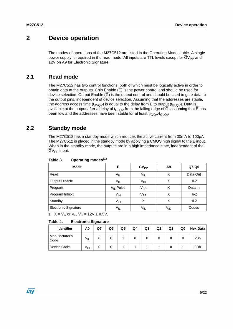
2 Device operation
The modes of operations of the M27C512 are listed in the Operating Modes table. A single power supply is required in the read mode. All inputs are TTL levels except for GVPP and 12V on A9 for Electronic Signature.
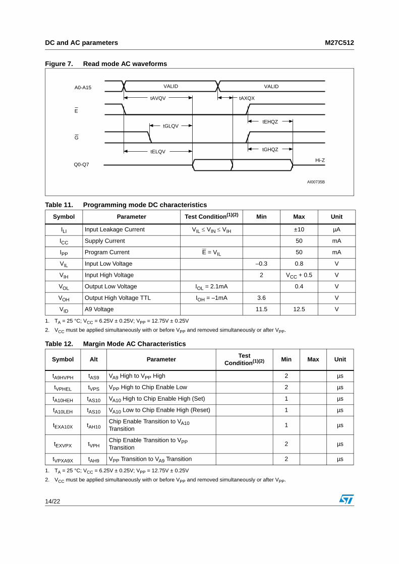
2.1 Read mode The M27C512 has two control functions, both of which must be logically active in order to obtain data at the outputs. Chip Enable (E) is the power control and should be used for device selection. Output Enable (G) is the output control and should be used to gate data to the output pins, independent of device selection. Assuming that the addresses are stable, the address access time (tAVQV) is equal to the delay from E to output (tELQV). Data is available at the output after a delay of tGLQV from the falling edge of G, assuming that E has been low and the addresses have been stable for at least tAVQV-tGLQV.
2.2 Standby mode The M27C512 has a standby mode which reduces the active current from 30mA to 100µA The M27C512 is placed in the standby mode by applying a CMOS high signal to the E input. When in the standby mode, the outputs are in a high impedance state, independent of the GVPP input.
Table 3. Operating modes(1)
1. X = VIH or VIL, VID = 12V ± 0.5V.
Mode E GVPP A9 Q7-Q0
Read VIL VIL X Data Out
Output Disable VIL VIH X Hi-Z
Program VIL Pulse VPP X Data In
Program Inhibit VIH VPP X Hi-Z
Standby VIH X X Hi-Z
Electronic Signature VIL VIL VID Codes
Table 4. Electronic Signature
Identifier A0 Q7 Q6 Q5 Q4 Q3 Q2 Q1 Q0 Hex Data
Manufacturer’s Code
VIL 0 0 1 0 0 0 0 0 20h
Device Code VIH 0 0 1 1 1 1 0 1 3Dh
Device operation M27C512
6/22
2.3 Two line output control Because EPROMs are usually used in larger memory arrays, the product features a 2 line control function which accommodates the use of multiple memory connection. The two line control function allows:
The lowest possible memory power dissipation,
Complete assurance that output bus contention will not occur.
For the most efficient use of these two control lines, E should be decoded and used as the primary device selecting function, while G should be made a common connection to all devices in the array and connected to the READ line from the system control bus. This ensures that all deselected memory devices are in their low power standby mode and that the output pins are only active when data is required from a particular memory device.
2.4 System considerations The power switching characteristics of Advanced CMOS EPROMs require careful decoupling of the devices. The supply current, ICC, has three segments that are of interest to the system designer: the standby current level, the active current level, and transient current peaks that are produced by the falling and rising edges of E. The magnitude of the transient current peaks is dependent on the capacitive and inductive loading of the device at the output. The associated transient voltage peaks can be suppressed by complying with the two line output control and by properly selected decoupling capacitors. It is recommended that a 0.1µF ceramic capacitor be used on every device between VCC and VSS. This should be a high frequency capacitor of low inherent inductance and should be placed as close to the device as possible. In addition, a 4.7µF bulk electrolytic capacitor should be used between VCC and VSS for every eight devices. The bulk capacitor should be located near the power supply connection point.The purpose of the bulk capacitor is to overcome the voltage drop caused by the inductive effects of PCB traces.
M27C512 Device operation
7/22
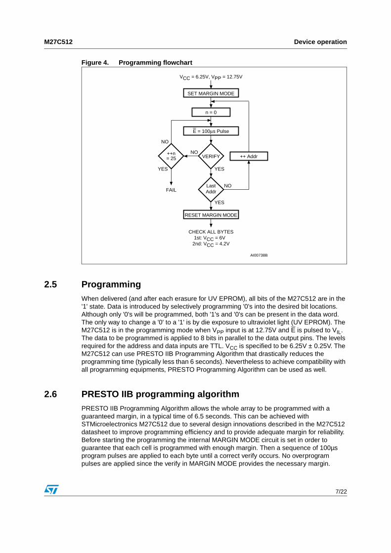
Figure 4. Programming flowchart
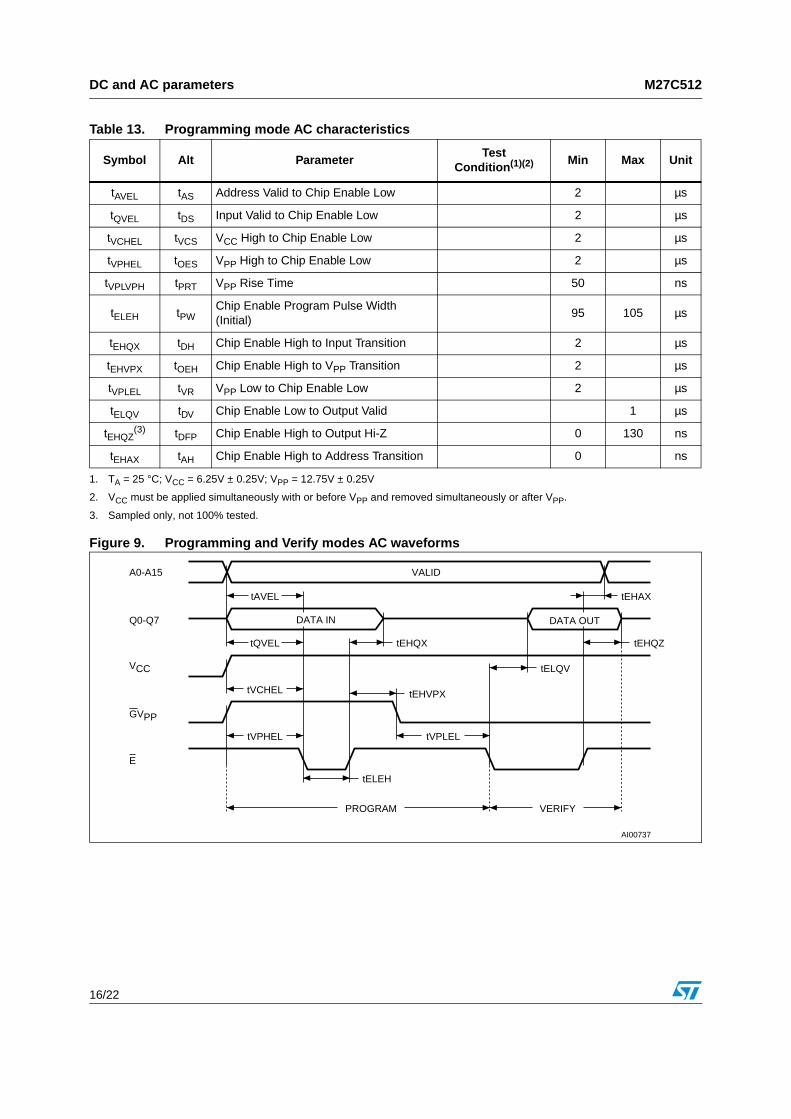
2.5 ProgrammingWhen delivered (and after each erasure for UV EPROM), all bits of the M27C512 are in the '1' state. Data is introduced by selectively programming '0's into the desired bit locations. Although only '0's will be programmed, both '1's and '0's can be present in the data word. The only way to change a '0' to a '1' is by die exposure to ultraviolet light (UV EPROM). The M27C512 is in the programming mode when VPP input is at 12.75V and E is pulsed to VIL. The data to be programmed is applied to 8 bits in parallel to the data output pins. The levels required for the address and data inputs are TTL. VCC is specified to be 6.25V ± 0.25V. The M27C512 can use PRESTO IIB Programming Algorithm that drastically reduces the programming time (typically less than 6 seconds). Nevertheless to achieve compatibility with all programming equipments, PRESTO Programming Algorithm can be used as well.
2.6 PRESTO IIB programming algorithm PRESTO IIB Programming Algorithm allows the whole array to be programmed with a guaranteed margin, in a typical time of 6.5 seconds. This can be achieved with STMicroelectronics M27C512 due to several design innovations described in the M27C512 datasheet to improve programming efficiency and to provide adequate margin for reliability. Before starting the programming the internal MARGIN MODE circuit is set in order to guarantee that each cell is programmed with enough margin. Then a sequence of 100µs program pulses are applied to each byte until a correct verify occurs. No overprogram pulses are applied since the verify in MARGIN MODE provides the necessary margin.
AI00738B
n = 0
LastAddr
VERIFY
E = 100µs Pulse
++n= 25 ++ Addr
VCC = 6.25V, VPP = 12.75V
FAIL
CHECK ALL BYTES1st: VCC = 6V
2nd: VCC = 4.2V
YES
NO
YES
NO
YES
NO
SET MARGIN MODE
RESET MARGIN MODE
Device operation M27C512
8/22
2.7 Program InhibitProgramming of multiple M27C512s in parallel with different data is also easily accomplished. Except for E, all like inputs including GVPP of the parallel M27C512 may be common. A TTL low level pulse applied to a M27C512's E input, with VPP at 12.75V, will program that M27C512. A high level E input inhibits the other M27C512s from being programmed.
2.8 Program VerifyA verify (read) should be performed on the programmed bits to determine that they were correctly programmed. The verify is accomplished with G at VIL. Data should be verified with tELQV after the falling edge of E.
2.9 Electronic SignatureThe Electronic Signature (ES) mode allows the reading out of a binary code from an EPROM that will identify its manufacturer and type. This mode is intended for use by programming equipment to automatically match the device to be programmed with its corresponding programming algorithm. The ES mode is functional in the 25°C ± 5°C ambient temperature range that is required when programming the M27C512. To activate the ES mode, the programming equipment must force 11.5V to 12.5V on address line A9 of the M27C512. Two identifier bytes may then be sequenced from the device outputs by toggling address line A0 from VIL to VIH. All other address lines must be held at VIL during Electronic Signature mode. Byte 0 (A0 = VIL) represents the manufacturer code and byte 1 (A0 = VIH) the device identifier code. For the STMicroelectronics M27C512, these two identifier bytes are given in <Blue>Table 4. and can be read-out on outputs Q7 to Q0.
M27C512 Erasure operation (applies for UV EPROM)
9/22
3 Erasure operation (applies for UV EPROM)
The erasure characteristics of the M27C512 is such that erasure begins when the cells are exposed to light with wavelengths shorter than approximately 4000 Å. It should be noted that sunlight and some type of fluorescent lamps have wavelengths in the 3000-4000 Å range.
Research shows that constant exposure to room level fluorescent lighting could erase a typical M27C512 in about 3 years, while it would take approximately 1 week to cause erasure when exposed to direct sunlight. If the M27C512 is to be exposed to these types of lighting conditions for extended periods of time, it is suggested that opaque labels be put over the M27C512 window to prevent unintentional erasure. The recommended erasure procedure for the M27C512 is exposure to short wave ultraviolet light which has wavelength 2537 Å. The integrated dose (i.e. UV intensity x exposure time) for erasure should be a minimum of 15 W-sec/cm2. The erasure time with this dosage is approximately 15 to 20 minutes using an ultraviolet lamp with 12000 µW/cm2 power rating. The M27C512 should be placed within 2.5 cm (1 inch) of the lamp tubes during the erasure. Some lamps have a filter on their tubes which should be removed before erasure.
Maximum rating M27C512
10/22
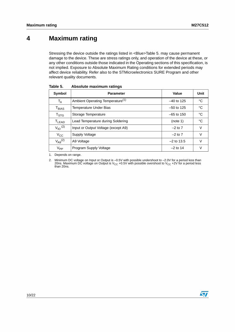
4 Maximum rating
Stressing the device outside the ratings listed in <Blue>Table 5. may cause permanent damage to the device. These are stress ratings only, and operation of the device at these, or any other conditions outside those indicated in the Operating sections of this specification, is not implied. Exposure to Absolute Maximum Rating conditions for extended periods may affect device reliability. Refer also to the STMicroelectronics SURE Program and other relevant quality documents.
Table 5. Absolute maximum ratings
Symbol Parameter Value Unit
TA Ambient Operating Temperature(1)
1. Depends on range.
–40 to 125 °C
TBIAS Temperature Under Bias –50 to 125 °C
TSTG Storage Temperature –65 to 150 °C
TLEAD Lead Temperature during Soldering (note 1) °C
VIO (2)
2. Minimum DC voltage on Input or Output is –0.5V with possible undershoot to –2.0V for a period less than 20ns. Maximum DC voltage on Output is VCC +0.5V with possible overshoot to VCC +2V for a period less than 20ns.
Input or Output Voltage (except A9) –2 to 7 V
VCC Supply Voltage –2 to 7 V
VA9(2) A9 Voltage –2 to 13.5 V
VPP Program Supply Voltage –2 to 14 V
M27C512 DC and AC parameters
11/22
5 DC and AC parameters
This section summarizes the operating and measurement conditions, and the DC and AC characteristics of the device. The parameters in the DC and AC Characteristic tables that follow are derived from tests performed under the Measurement Conditions summarized in the relevant tables. Designers should check that the operating conditions in their circuit match the measurement conditions when relying on the quoted parameters.
Figure 5. Testing input/output waveform
Figure 6. AC Testing Load Circuit
Table 6. AC measurement conditions
High Speed Standard
Input Rise and Fall Times ≤ 10ns ≤ 20ns
Input Pulse Voltages 0 to 3V 0.4V to 2.4V
Input and Output Timing Ref. Voltages 1.5V 0.8V and 2V
AI01822
3V
High Speed
0V
1.5V
2.4V
Standard
0.4V
2.0V
0.8V
AI01823B
1.3V
OUT
CL
CL = 30pF for High Speed
CL = 100pF for Standard
CL includes JIG capacitance
3.3kΩ
1N914
DEVICEUNDERTEST
DC and AC parameters M27C512
12/22
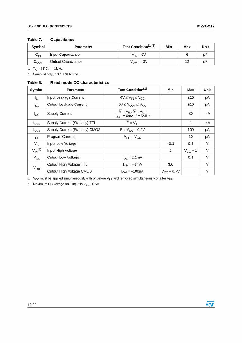
Table 7. Capacitance
Symbol Parameter Test Condition(1)(2) Min Max Unit
CIN Input Capacitance VIN = 0V 6 pF
COUT Output Capacitance VOUT = 0V 12 pF
1. TA = 25°C, f = 1MHz
2. Sampled only, not 100% tested.
Table 8. Read mode DC characteristics
Symbol Parameter Test Condition(1) Min Max Unit
ILI Input Leakage Current 0V ≤ VIN ≤ VCC ±10 µA
ILO Output Leakage Current 0V ≤ VOUT ≤ VCC ±10 µA
ICC Supply CurrentE = VIL, G = VIL,
IOUT = 0mA, f = 5MHz30 mA
ICC1 Supply Current (Standby) TTL E = VIH 1 mA
ICC2 Supply Current (Standby) CMOS E > VCC – 0.2V 100 µA
IPP Program Current VPP = VCC 10 µA
VIL Input Low Voltage –0.3 0.8 V
VIH(2) Input High Voltage 2 VCC + 1 V
VOL Output Low Voltage IOL = 2.1mA 0.4 V
VOH
Output High Voltage TTL IOH = –1mA 3.6 V
Output High Voltage CMOS IOH = –100µA VCC – 0.7V V
1. VCC must be applied simultaneously with or before VPP and removed simultaneously or after VPP.
2. Maximum DC voltage on Output is VCC +0.5V.
M27C512 DC and AC parameters
13/22
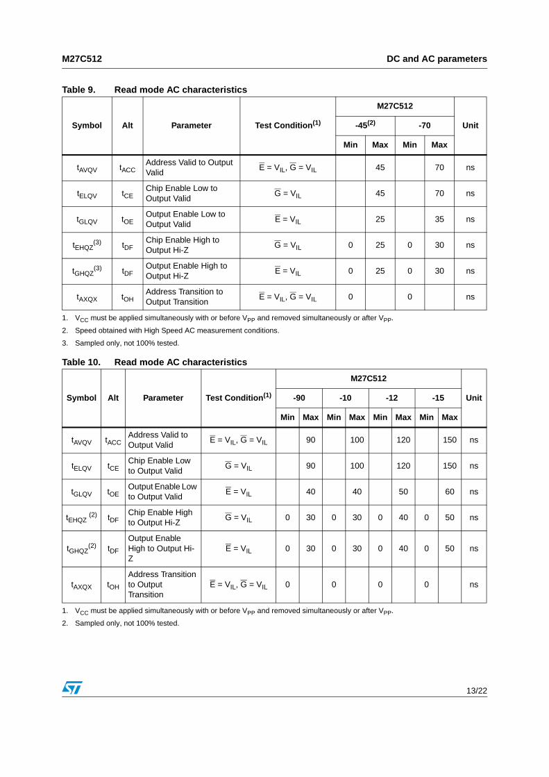
Table 9. Read mode AC characteristics
Symbol Alt Parameter Test Condition(1)
M27C512
Unit -45(2) -70
Min Max Min Max
tAVQV tACCAddress Valid to Output Valid
E = VIL, G = VIL 45 70 ns
tELQV tCEChip Enable Low to Output Valid
G = VIL 45 70 ns
tGLQV tOEOutput Enable Low to Output Valid
E = VIL 25 35 ns
tEHQZ(3) tDF
Chip Enable High to Output Hi-Z
G = VIL 0 25 0 30 ns
tGHQZ(3) tDF
Output Enable High to Output Hi-Z
E = VIL 0 25 0 30 ns
tAXQX tOHAddress Transition to Output Transition
E = VIL, G = VIL 0 0 ns
1. VCC must be applied simultaneously with or before VPP and removed simultaneously or after VPP.
2. Speed obtained with High Speed AC measurement conditions.
3. Sampled only, not 100% tested.
Table 10. Read mode AC characteristics
Symbol Alt Parameter Test Condition(1)
M27C512
Unit -90 -10 -12 -15
Min Max Min Max Min Max Min Max
tAVQV tACCAddress Valid to Output Valid
E = VIL, G = VIL 90 100 120 150 ns
tELQV tCEChip Enable Low to Output Valid
G = VIL 90 100 120 150 ns
tGLQV tOEOutput Enable Low to Output Valid
E = VIL 40 40 50 60 ns
tEHQZ (2) tDFChip Enable High to Output Hi-Z
G = VIL 0 30 0 30 0 40 0 50 ns
tGHQZ(2) tDF
Output Enable High to Output Hi-Z
E = VIL 0 30 0 30 0 40 0 50 ns
tAXQX tOH
Address Transition to Output Transition
E = VIL, G = VIL 0 0 0 0 ns
1. VCC must be applied simultaneously with or before VPP and removed simultaneously or after VPP.
2. Sampled only, not 100% tested.
DC and AC parameters M27C512
14/22
Figure 7. Read mode AC waveforms
AI00735B
tAXQX
tEHQZ
A0-A15
E
G
Q0-Q7
tAVQV
tGHQZ
tGLQV
tELQV
VALID
Hi-Z
VALID
Table 11. Programming mode DC characteristics
Symbol Parameter Test Condition(1)(2) Min Max Unit
ILI Input Leakage Current VIL ≤ VIN ≤ VIH ±10 µA
ICC Supply Current 50 mA
IPP Program Current E = VIL 50 mA
VIL Input Low Voltage –0.3 0.8 V
VIH Input High Voltage 2 VCC + 0.5 V
VOL Output Low Voltage IOL = 2.1mA 0.4 V
VOH Output High Voltage TTL IOH = –1mA 3.6 V
VID A9 Voltage 11.5 12.5 V
1. TA = 25 °C; VCC = 6.25V ± 0.25V; VPP = 12.75V ± 0.25V
2. VCC must be applied simultaneously with or before VPP and removed simultaneously or after VPP.
Table 12. Margin Mode AC Characteristics
Symbol Alt ParameterTest
Condition(1)(2) Min Max Unit
tA9HVPH tAS9 VA9 High to VPP High 2 µs
tVPHEL tVPS VPP High to Chip Enable Low 2 µs
tA10HEH tAS10 VA10 High to Chip Enable High (Set) 1 µs
tA10LEH tAS10 VA10 Low to Chip Enable High (Reset) 1 µs
tEXA10X tAH10Chip Enable Transition to VA10 Transition
1 µs
tEXVPX tVPHChip Enable Transition to VPP Transition
2 µs
tVPXA9X tAH9 VPP Transition to VA9 Transition 2 µs
1. TA = 25 °C; VCC = 6.25V ± 0.25V; VPP = 12.75V ± 0.25V
2. VCC must be applied simultaneously with or before VPP and removed simultaneously or after VPP.
M27C512 DC and AC parameters
15/22
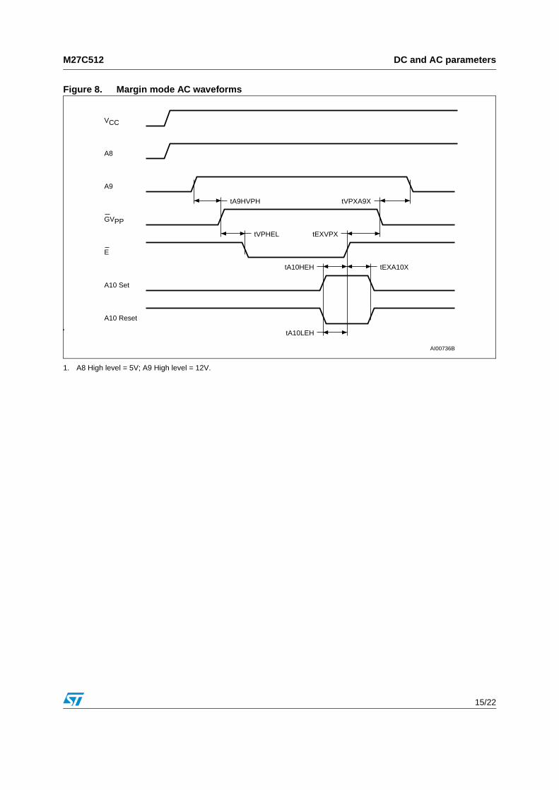
Figure 8. Margin mode AC waveforms
1. A8 High level = 5V; A9 High level = 12V.
AI00736B
tA9HVPH tVPXA9X
A8
E
GVPP
A10 Set
VCC
tVPHEL
tA10LEH
tEXVPX
tA10HEH
A9
A10 Reset
tEXA10X
DC and AC parameters M27C512
16/22
Figure 9. Programming and Verify modes AC waveforms
Table 13. Programming mode AC characteristics
Symbol Alt ParameterTest
Condition(1)(2) Min Max Unit
tAVEL tAS Address Valid to Chip Enable Low 2 µs
tQVEL tDS Input Valid to Chip Enable Low 2 µs
tVCHEL tVCS VCC High to Chip Enable Low 2 µs
tVPHEL tOES VPP High to Chip Enable Low 2 µs
tVPLVPH tPRT VPP Rise Time 50 ns
tELEH tPWChip Enable Program Pulse Width (Initial)
95 105 µs
tEHQX tDH Chip Enable High to Input Transition 2 µs
tEHVPX tOEH Chip Enable High to VPP Transition 2 µs
tVPLEL tVR VPP Low to Chip Enable Low 2 µs
tELQV tDV Chip Enable Low to Output Valid 1 µs
tEHQZ(3) tDFP Chip Enable High to Output Hi-Z 0 130 ns
tEHAX tAH Chip Enable High to Address Transition 0 ns
1. TA = 25 °C; VCC = 6.25V ± 0.25V; VPP = 12.75V ± 0.25V
2. VCC must be applied simultaneously with or before VPP and removed simultaneously or after VPP.
3. Sampled only, not 100% tested.
AI00737
tVPLEL
PROGRAM
DATA IN
A0-A15
E
GVPP
Q0-Q7 DATA OUT
tAVEL
tQVEL
tVCHEL
tVPHEL
tEHQX
tEHVPX
tELEH
tELQV
tEHAX
tEHQZ
VERIFY
VALID
VCC
M27C512 Package mechanical
17/22
6 Package mechanical
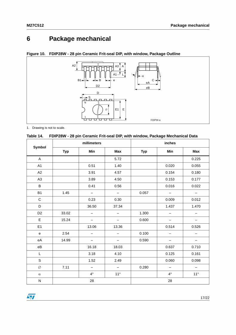
Figure 10. FDIP28W - 28 pin Ceramic Frit-seal DIP, with window, Package Outline
1. Drawing is not to scale.
FDIPW-a
A3
A1
A
L
B1 B e
D
S
E1 E
N
1
Cα
eAD2
∅
eB
A2
Table 14. FDIP28W - 28 pin Ceramic Frit-seal DIP, with window, Package Mechanical Data
Symbolmillimeters inches
Typ Min Max Typ Min Max
A 5.72 0.225
A1 0.51 1.40 0.020 0.055
A2 3.91 4.57 0.154 0.180
A3 3.89 4.50 0.153 0.177
B 0.41 0.56 0.016 0.022
B1 1.45 – – 0.057 – –
C 0.23 0.30 0.009 0.012
D 36.50 37.34 1.437 1.470
D2 33.02 – – 1.300 – –
E 15.24 – – 0.600 – –
E1 13.06 13.36 0.514 0.526
e 2.54 – – 0.100 – –
eA 14.99 – – 0.590 – –
eB 16.18 18.03 0.637 0.710
L 3.18 4.10 0.125 0.161
S 1.52 2.49 0.060 0.098
∅ 7.11 – – 0.280 – –
α 4° 11° 4° 11°
N 28 28
Package mechanical M27C512
18/22
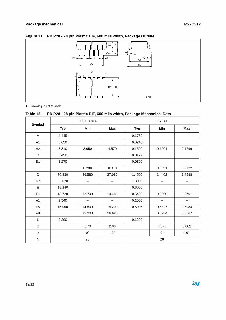
Figure 11. PDIP28 - 28 pin Plastic DIP, 600 mils width, Package Outline
1. Drawing is not to scale.
PDIP
A2
A1
A
L
B1 B e1
D
S
E1 E
N
1
Cα
eA
eBD2
Table 15. PDIP28 - 28 pin Plastic DIP, 600 mils width, Package Mechanical Data
Symbolmillimeters inches
Typ Min Max Typ Min Max
A 4.445 0.1750
A1 0.630 0.0248
A2 3.810 3.050 4.570 0.1500 0.1201 0.1799
B 0.450 0.0177
B1 1.270 0.0500
C 0.230 0.310 0.0091 0.0122
D 36.830 36.580 37.080 1.4500 1.4402 1.4598
D2 33.020 – – 1.3000 – –
E 15.240 0.6000
E1 13.720 12.700 14.480 0.5402 0.5000 0.5701
e1 2.540 – – 0.1000 – –
eA 15.000 14.800 15.200 0.5906 0.5827 0.5984
eB 15.200 16.680 0.5984 0.6567
L 3.300 0.1299
S 1.78 2.08 0.070 0.082
α 0° 10° 0° 10°
N 28 28
M27C512 Package mechanical
19/22
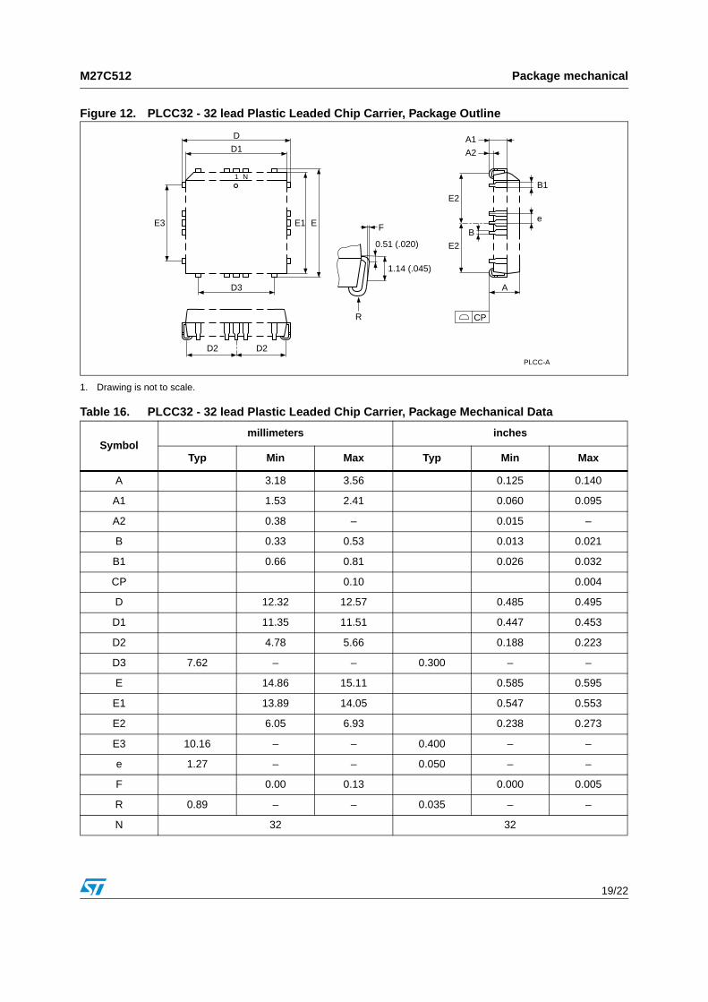
Figure 12. PLCC32 - 32 lead Plastic Leaded Chip Carrier, Package Outline
1. Drawing is not to scale.
PLCC-A
D
E3 E1 E
1 N
D1
D3
CP
B
E2
e
B1
A1
A
R
0.51 (.020)
1.14 (.045)
F
A2
E2
D2 D2
Table 16. PLCC32 - 32 lead Plastic Leaded Chip Carrier, Package Mechanical Data
Symbolmillimeters inches
Typ Min Max Typ Min Max
A 3.18 3.56 0.125 0.140
A1 1.53 2.41 0.060 0.095
A2 0.38 – 0.015 –
B 0.33 0.53 0.013 0.021
B1 0.66 0.81 0.026 0.032
CP 0.10 0.004
D 12.32 12.57 0.485 0.495
D1 11.35 11.51 0.447 0.453
D2 4.78 5.66 0.188 0.223
D3 7.62 – – 0.300 – –
E 14.86 15.11 0.585 0.595
E1 13.89 14.05 0.547 0.553
E2 6.05 6.93 0.238 0.273
E3 10.16 – – 0.400 – –
e 1.27 – – 0.050 – –
F 0.00 0.13 0.000 0.005
R 0.89 – – 0.035 – –
N 32 32
Part numbering M27C512
20/22
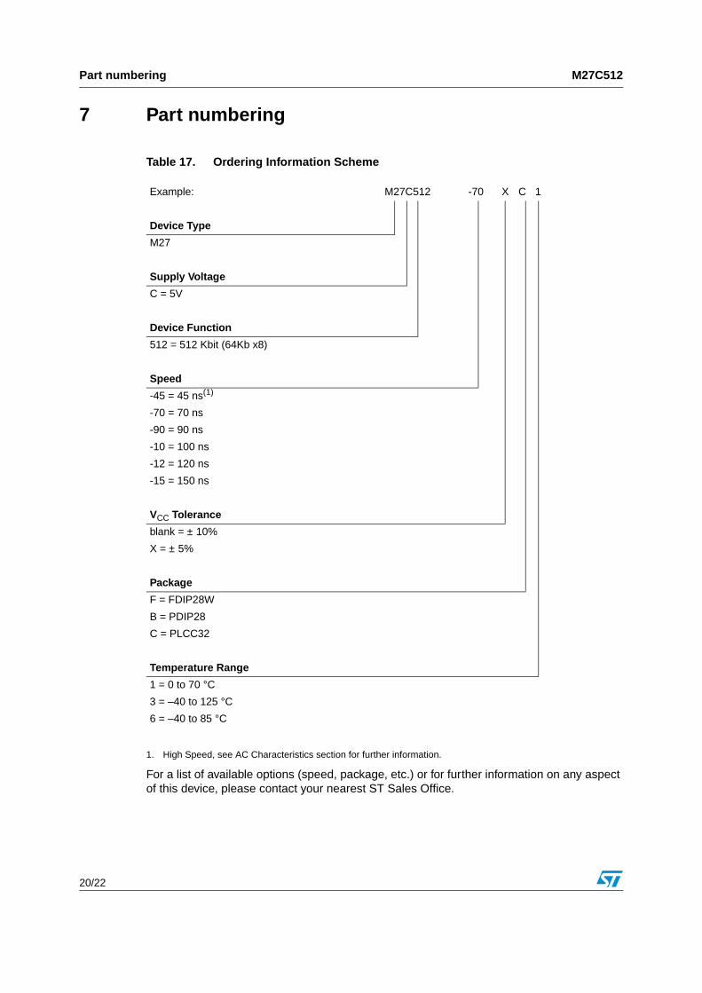
7 Part numbering
For a list of available options (speed, package, etc.) or for further information on any aspect of this device, please contact your nearest ST Sales Office.
Table 17. Ordering Information Scheme
Example: M27C512 -70 X C 1
Device Type
M27
Supply Voltage
C = 5V
Device Function
512 = 512 Kbit (64Kb x8)
Speed
-45 = 45 ns(1)
1. High Speed, see AC Characteristics section for further information.
-70 = 70 ns
-90 = 90 ns
-10 = 100 ns
-12 = 120 ns
-15 = 150 ns
VCC Tolerance
blank = ± 10%
X = ± 5%
Package
F = FDIP28W
B = PDIP28
C = PLCC32
Temperature Range
1 = 0 to 70 °C
3 = –40 to 125 °C
6 = –40 to 85 °C
M27C512 Revision history
21/22
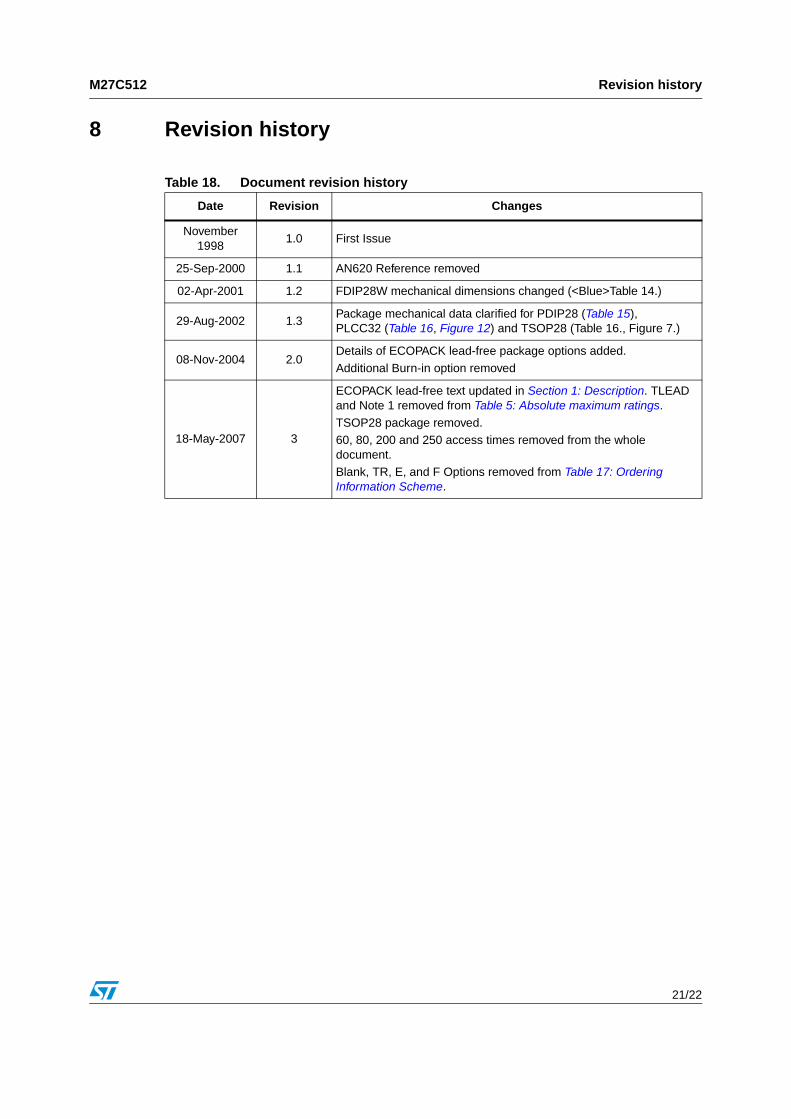
8 Revision history
Table 18. Document revision history
Date Revision Changes
November 1998
1.0 First Issue
25-Sep-2000 1.1 AN620 Reference removed
02-Apr-2001 1.2 FDIP28W mechanical dimensions changed (<Blue>Table 14.)
29-Aug-2002 1.3Package mechanical data clarified for PDIP28 (Table 15), PLCC32 (Table 16, Figure 12) and TSOP28 (Table 16., Figure 7.)
08-Nov-2004 2.0Details of ECOPACK lead-free package options added.
Additional Burn-in option removed
18-May-2007 3
ECOPACK lead-free text updated in Section 1: Description. TLEAD and Note 1 removed from Table 5: Absolute maximum ratings.
TSOP28 package removed. 60, 80, 200 and 250 access times removed from the whole document.Blank, TR, E, and F Options removed from Table 17: Ordering Information Scheme.
M27C512
22/22
Please Read Carefully:
Information in this document is provided solely in connection with ST products. STMicroelectronics NV and its subsidiaries (“ST”) reserve theright to make changes, corrections, modifications or improvements, to this document, and the products and services described herein at anytime, without notice.
All ST products are sold pursuant to ST’s terms and conditions of sale.
Purchasers are solely responsible for the choice, selection and use of the ST products and services described herein, and ST assumes noliability whatsoever relating to the choice, selection or use of the ST products and services described herein.
No license, express or implied, by estoppel or otherwise, to any intellectual property rights is granted under this document. If any part of thisdocument refers to any third party products or services it shall not be deemed a license grant by ST for the use of such third party productsor services, or any intellectual property contained therein or considered as a warranty covering the use in any manner whatsoever of suchthird party products or services or any intellectual property contained therein.
UNLESS OTHERWISE SET FORTH IN ST’S TERMS AND CONDITIONS OF SALE ST DISCLAIMS ANY EXPRESS OR IMPLIEDWARRANTY WITH RESPECT TO THE USE AND/OR SALE OF ST PRODUCTS INCLUDING WITHOUT LIMITATION IMPLIEDWARRANTIES OF MERCHANTABILITY, FITNESS FOR A PARTICULAR PURPOSE (AND THEIR EQUIVALENTS UNDER THE LAWSOF ANY JURISDICTION), OR INFRINGEMENT OF ANY PATENT, COPYRIGHT OR OTHER INTELLECTUAL PROPERTY RIGHT.
UNLESS EXPRESSLY APPROVED IN WRITING BY AN AUTHORIZED ST REPRESENTATIVE, ST PRODUCTS ARE NOTRECOMMENDED, AUTHORIZED OR WARRANTED FOR USE IN MILITARY, AIR CRAFT, SPACE, LIFE SAVING, OR LIFE SUSTAININGAPPLICATIONS, NOR IN PRODUCTS OR SYSTEMS WHERE FAILURE OR MALFUNCTION MAY RESULT IN PERSONAL INJURY,DEATH, OR SEVERE PROPERTY OR ENVIRONMENTAL DAMAGE. ST PRODUCTS WHICH ARE NOT SPECIFIED AS "AUTOMOTIVEGRADE" MAY ONLY BE USED IN AUTOMOTIVE APPLICATIONS AT USER’S OWN RISK.
Resale of ST products with provisions different from the statements and/or technical features set forth in this document shall immediately voidany warranty granted by ST for the ST product or service described herein and shall not create or extend in any manner whatsoever, anyliability of ST.
ST and the ST logo are trademarks or registered trademarks of ST in various countries.
Information in this document supersedes and replaces all information previously supplied.
The ST logo is a registered trademark of STMicroelectronics. All other names are the property of their respective owners.
© 2007 STMicroelectronics - All rights reserved
STMicroelectronics group of companies
Australia - Belgium - Brazil - Canada - China - Czech Republic - Finland - France - Germany - Hong Kong - India - Israel - Italy - Japan - Malaysia - Malta - Morocco - Singapore - Spain - Sweden - Switzerland - United Kingdom - United States of America
www.st.com