Embed Size (px)
Citation preview
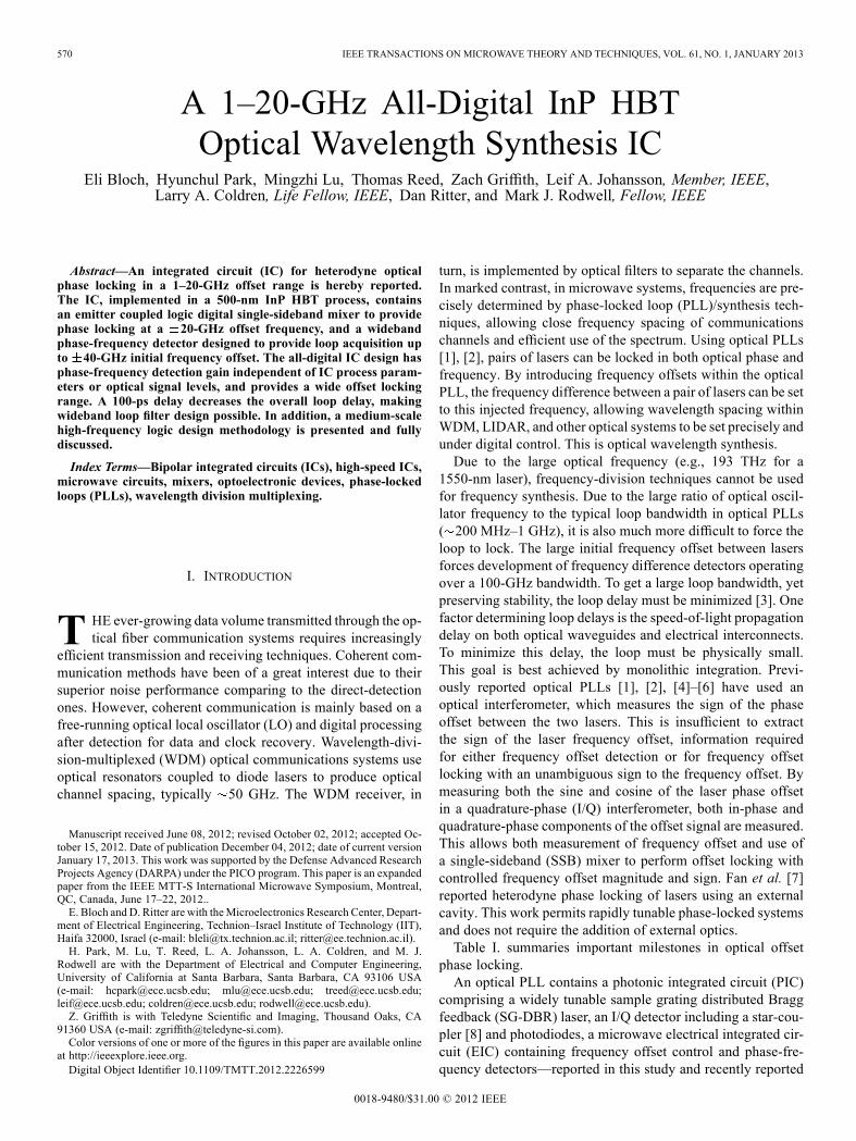
570 IEEE TRANSACTIONS ON MICROWAVE THEORY AND TECHNIQUES, VOL. 61, NO. 1, JANUARY 2013
A 1–20-GHz All-Digital InP HBTOptical Wavelength Synthesis IC
Eli Bloch, Hyunchul Park, Mingzhi Lu, Thomas Reed, Zach Griffith, Leif A. Johansson, Member, IEEE,Larry A. Coldren, Life Fellow, IEEE, Dan Ritter, and Mark J. Rodwell, Fellow, IEEE
Abstract—An integrated circuit (IC) for heterodyne opticalphase locking in a 1–20-GHz offset range is hereby reported.The IC, implemented in a 500-nm InP HBT process, containsan emitter coupled logic digital single-sideband mixer to providephase locking at a 20-GHz offset frequency, and a widebandphase-frequency detector designed to provide loop acquisition upto 40-GHz initial frequency offset. The all-digital IC design hasphase-frequency detection gain independent of IC process param-eters or optical signal levels, and provides a wide offset lockingrange. A 100-ps delay decreases the overall loop delay, makingwideband loop filter design possible. In addition, a medium-scalehigh-frequency logic design methodology is presented and fullydiscussed.
Index Terms—Bipolar integrated circuits (ICs), high-speed ICs,microwave circuits, mixers, optoelectronic devices, phase-lockedloops (PLLs), wavelength division multiplexing.
I. INTRODUCTION
T HE ever-growing data volume transmitted through the op-tical fiber communication systems requires increasingly
efficient transmission and receiving techniques. Coherent com-munication methods have been of a great interest due to theirsuperior noise performance comparing to the direct-detectionones. However, coherent communication is mainly based on afree-running optical local oscillator (LO) and digital processingafter detection for data and clock recovery. Wavelength-divi-sion-multiplexed (WDM) optical communications systems useoptical resonators coupled to diode lasers to produce opticalchannel spacing, typically 50 GHz. The WDM receiver, in
Manuscript received June 08, 2012; revised October 02, 2012; accepted Oc-tober 15, 2012. Date of publication December 04, 2012; date of current versionJanuary 17, 2013. This work was supported by the Defense Advanced ResearchProjects Agency (DARPA) under the PICO program. This paper is an expandedpaper from the IEEE MTT-S International Microwave Symposium, Montreal,QC, Canada, June 17–22, 2012..E. Bloch and D. Ritter are with theMicroelectronics Research Center, Depart-
ment of Electrical Engineering, Technion–Israel Institute of Technology (IIT),Haifa 32000, Israel (e-mail: [email protected]; [email protected]).H. Park, M. Lu, T. Reed, L. A. Johansson, L. A. Coldren, and M. J.
Rodwell are with the Department of Electrical and Computer Engineering,University of California at Santa Barbara, Santa Barbara, CA 93106 USA(e-mail: [email protected]; [email protected]; [email protected];[email protected]; [email protected]; [email protected]).Z. Griffith is with Teledyne Scientific and Imaging, Thousand Oaks, CA
91360 USA (e-mail: [email protected]).Color versions of one or more of the figures in this paper are available online
at http://ieeexplore.ieee.org.Digital Object Identifier 10.1109/TMTT.2012.2226599
turn, is implemented by optical filters to separate the channels.In marked contrast, in microwave systems, frequencies are pre-cisely determined by phase-locked loop (PLL)/synthesis tech-niques, allowing close frequency spacing of communicationschannels and efficient use of the spectrum. Using optical PLLs[1], [2], pairs of lasers can be locked in both optical phase andfrequency. By introducing frequency offsets within the opticalPLL, the frequency difference between a pair of lasers can be setto this injected frequency, allowing wavelength spacing withinWDM, LIDAR, and other optical systems to be set precisely andunder digital control. This is optical wavelength synthesis.Due to the large optical frequency (e.g., 193 THz for a
1550-nm laser), frequency-division techniques cannot be usedfor frequency synthesis. Due to the large ratio of optical oscil-lator frequency to the typical loop bandwidth in optical PLLs( 200 MHz–1 GHz), it is also much more difficult to force theloop to lock. The large initial frequency offset between lasersforces development of frequency difference detectors operatingover a 100-GHz bandwidth. To get a large loop bandwidth, yetpreserving stability, the loop delay must be minimized [3]. Onefactor determining loop delays is the speed-of-light propagationdelay on both optical waveguides and electrical interconnects.To minimize this delay, the loop must be physically small.This goal is best achieved by monolithic integration. Previ-ously reported optical PLLs [1], [2], [4]–[6] have used anoptical interferometer, which measures the sign of the phaseoffset between the two lasers. This is insufficient to extractthe sign of the laser frequency offset, information requiredfor either frequency offset detection or for frequency offsetlocking with an unambiguous sign to the frequency offset. Bymeasuring both the sine and cosine of the laser phase offsetin a quadrature-phase (I/Q) interferometer, both in-phase andquadrature-phase components of the offset signal are measured.This allows both measurement of frequency offset and use ofa single-sideband (SSB) mixer to perform offset locking withcontrolled frequency offset magnitude and sign. Fan et al. [7]reported heterodyne phase locking of lasers using an externalcavity. This work permits rapidly tunable phase-locked systemsand does not require the addition of external optics.Table I. summaries important milestones in optical offset
phase locking.An optical PLL contains a photonic integrated circuit (PIC)
comprising a widely tunable sample grating distributed Braggfeedback (SG-DBR) laser, an I/Q detector including a star-cou-pler [8] and photodiodes, a microwave electrical integrated cir-cuit (EIC) containing frequency offset control and phase-fre-quency detectors—reported in this study and recently reported
0018-9480/$31.00 © 2012 IEEE
BLOCH et al.: 1–20-GHz ALL-DIGITAL InP HBT OPTICAL WAVELENGTH SYNTHESIS IC 571
TABLE IHETERODYNE OPTICAL PHASE LOCKING—PARALLEL STUDIES
in [9], and a high-frequency (500 MHz), low-delay feed-for-ward-compensated op-amp loop-filter [10]. PIC design and op-tical wavelength synthesis results are reported in [11]. Here, wereport the design methodology and performance of an InP HBToptical wavelength synthesis IC comprised of a 1–20-GHz dig-ital SSB mixer and a 40-GHz phase-frequency difference de-tector (PFD). The digital design eliminates the dependence ofloop bandwidth on optical signal levels (i.e., input photocurrentmagnitudes) and enables a wide frequency locking range. In thispaper, optical heterodyne locking methods and considerationsare examined, a novel digital mixing technique is in-depth an-alyzed, and design methodologies of complex high-frequencydigital ICs are discussed.
II. OPTICAL SYNTHESIZER DESIGN
Optical and electrical PLLs differ fundamentally in thatthe ratio of carrier frequency to loop bandwidth is a ratio of10 1 larger in optical than in electrical PLLs. This vast
ratio of oscillator frequency to loop bandwidth has a profoundimpact upon the range of wavelengths over which an opticalPLL will acquire lock, and greatly impairs the rate both atwhich the optical PLL can scan its frequency and its absolutefrequency tuning range.The wide ( 200 GHz) frequency tuning range of semicon-
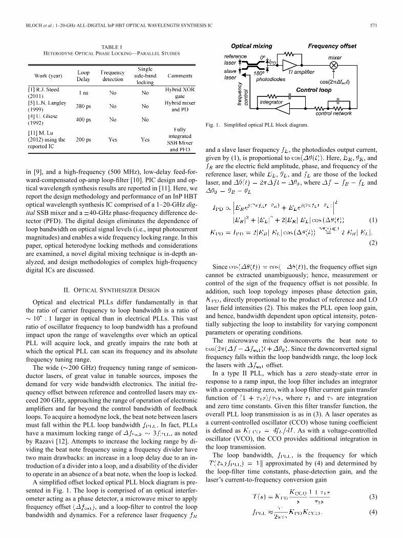
ductor lasers, of great value in tunable sources, imposes thedemand for very wide bandwidth electronics. The initial fre-quency offset between reference and controlled lasers may ex-ceed 200 GHz, approaching the range of operation of electronicamplifiers and far beyond the control bandwidth of feedbackloops. To acquire a homodyne lock, the beat note between lasersmust fall within the PLL loop bandwidth . In fact, PLLshave a maximum locking range of 3 , as notedby Razavi [12]. Attempts to increase the locking range by di-viding the beat note frequency using a frequency divider havetwo main drawbacks: an increase in a loop delay due to an in-troduction of a divider into a loop, and a disability of the dividerto operate in an absence of a beat note, when the loop is locked.A simplified offset locked optical PLL block diagram is pre-
sented in Fig. 1. The loop is comprised of an optical interfer-ometer acting as a phase detector, a microwave mixer to applyfrequency offset , and a loop-filter to control the loopbandwidth and dynamics. For a reference laser frequency
Fig. 1. Simplified optical PLL block diagram.
and a slave laser frequency , the photodiodes output current,given by (1), is proportional to . Here, , , andare the electric field amplitude, phase, and frequency of the
reference laser, while , , and are those of the lockedlaser, and , where and
(1)
(2)
Since , the frequency offset signcannot be extracted unambiguously; hence, measurement orcontrol of the sign of the frequency offset is not possible. Inaddition, such loop topology imposes phase detection gain,
, directly proportional to the product of reference and LOlaser field intensities (2). This makes the PLL open loop gain,and hence, bandwidth dependent upon optical intensity, poten-tially subjecting the loop to instability for varying componentparameters or operating conditions.The microwave mixer downconverts the beat note to
. Since the downconverted signalfrequency falls within the loop bandwidth range, the loop lockthe lasers with offset.In a type II PLL, which has a zero steady-state error in
response to a ramp input, the loop filter includes an integratorwith a compensating zero, with a loop filter current gain transferfunction of , where and are integrationand zero time constants. Given this filter transfer function, theoverall PLL loop transmission is as in (3). A laser operates asa current-controlled oscillator (CCO) whose tuning coefficientis defined as . As with a voltage-controlledoscillator (VCO), the CCO provides additional integration inthe loop transmission.The loop bandwidth, , is the frequency for which
approximated by (4) and determined bythe loop-filter time constants, phase-detection gain, and thelaser’s current-to-frequency conversion gain
(3)
(4)
572 IEEE TRANSACTIONS ON MICROWAVE THEORY AND TECHNIQUES, VOL. 61, NO. 1, JANUARY 2013
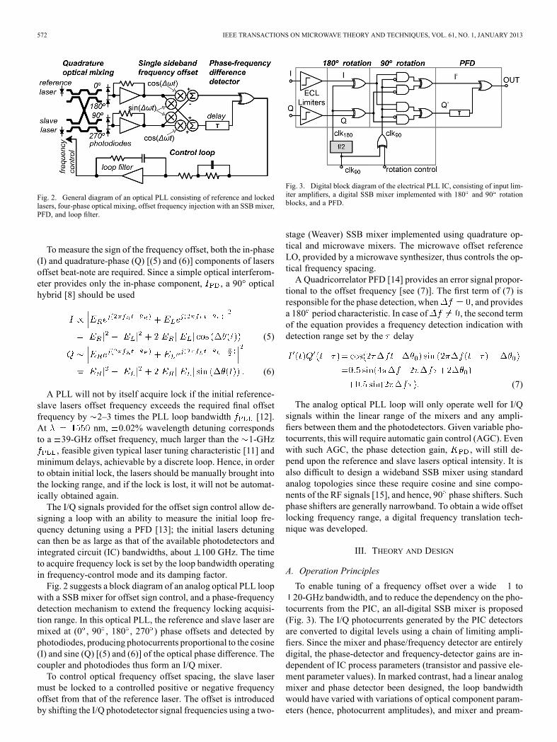
Fig. 2. General diagram of an optical PLL consisting of reference and lockedlasers, four-phase optical mixing, offset frequency injection with an SSB mixer,PFD, and loop filter.
To measure the sign of the frequency offset, both the in-phase(I) and quadrature-phase (Q) [(5) and (6)] components of lasersoffset beat-note are required. Since a simple optical interferom-eter provides only the in-phase component, , a 90° opticalhybrid [8] should be used
(5)
(6)
A PLL will not by itself acquire lock if the initial reference-slave lasers offset frequency exceeds the required final offsetfrequency by 2–3 times the PLL loop bandwidth [12].At nm, 0.02% wavelength detuning correspondsto a 39-GHz offset frequency, much larger than the 1-GHz
, feasible given typical laser tuning characteristic [11] andminimum delays, achievable by a discrete loop. Hence, in orderto obtain initial lock, the lasers should be manually brought intothe locking range, and if the lock is lost, it will not be automat-ically obtained again.The I/Q signals provided for the offset sign control allow de-
signing a loop with an ability to measure the initial loop fre-quency detuning using a PFD [13]; the initial lasers detuningcan then be as large as that of the available photodetectors andintegrated circuit (IC) bandwidths, about 100 GHz. The timeto acquire frequency lock is set by the loop bandwidth operatingin frequency-control mode and its damping factor.Fig. 2 suggests a block diagram of an analog optical PLL loop
with a SSB mixer for offset sign control, and a phase-frequencydetection mechanism to extend the frequency locking acquisi-tion range. In this optical PLL, the reference and slave laser aremixed at (0 , 90 , 180 , 270 ) phase offsets and detected byphotodiodes, producing photocurrents proportional to the cosine(I) and sine (Q) [(5) and (6)] of the optical phase difference. Thecoupler and photodiodes thus form an I/Q mixer.To control optical frequency offset spacing, the slave laser
must be locked to a controlled positive or negative frequencyoffset from that of the reference laser. The offset is introducedby shifting the I/Q photodetector signal frequencies using a two-
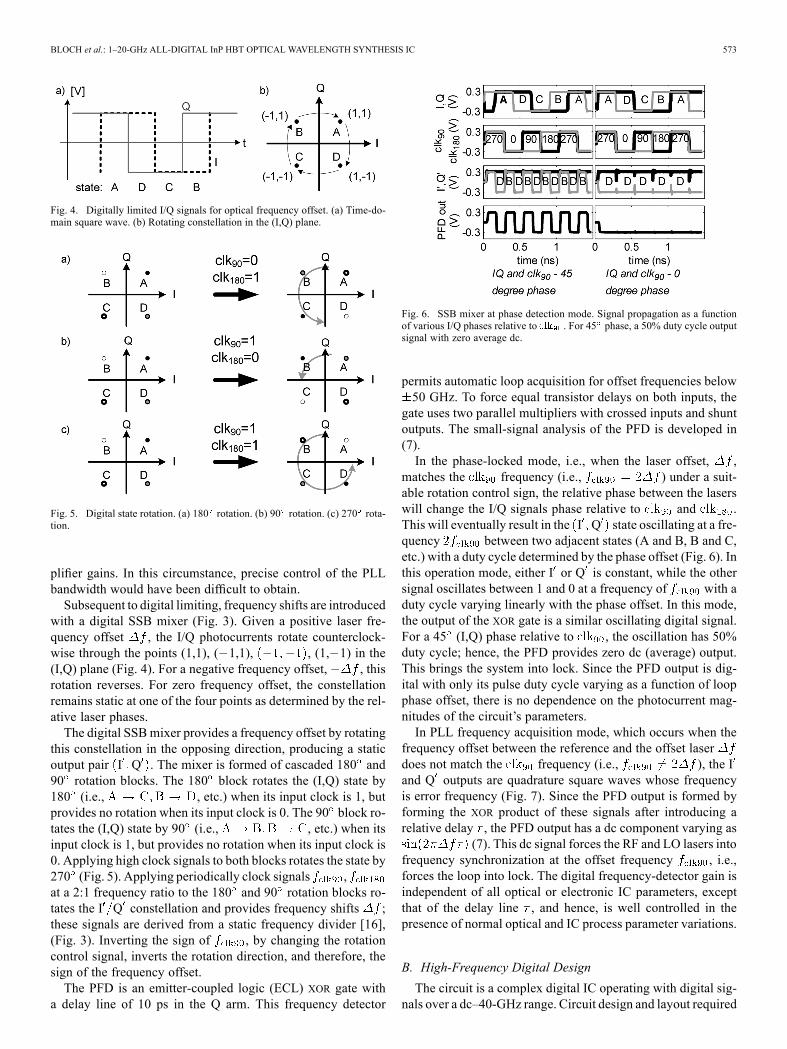
Fig. 3. Digital block diagram of the electrical PLL IC, consisting of input lim-iter amplifiers, a digital SSB mixer implemented with 180 and 90 rotationblocks, and a PFD.
stage (Weaver) SSB mixer implemented using quadrature op-tical and microwave mixers. The microwave offset referenceLO, provided by a microwave synthesizer, thus controls the op-tical frequency spacing.A Quadricorrelator PFD [14] provides an error signal propor-
tional to the offset frequency [see (7)]. The first term of (7) isresponsible for the phase detection, when , and providesa 180 period characteristic. In case of , the second termof the equation provides a frequency detection indication withdetection range set by the delay
(7)
The analog optical PLL loop will only operate well for I/Qsignals within the linear range of the mixers and any ampli-fiers between them and the photodetectors. Given variable pho-tocurrents, this will require automatic gain control (AGC). Evenwith such AGC, the phase detection gain, , will still de-pend upon the reference and slave lasers optical intensity. It isalso difficult to design a wideband SSB mixer using standardanalog topologies since these require cosine and sine compo-nents of the RF signals [15], and hence, 90 phase shifters. Suchphase shifters are generally narrowband. To obtain a wide offsetlocking frequency range, a digital frequency translation tech-nique was developed.
III. THEORY AND DESIGN
A. Operation Principles
To enable tuning of a frequency offset over a wide 1 to20-GHz bandwidth, and to reduce the dependency on the pho-
tocurrents from the PIC, an all-digital SSB mixer is proposed(Fig. 3). The I/Q photocurrents generated by the PIC detectorsare converted to digital levels using a chain of limiting ampli-fiers. Since the mixer and phase/frequency detector are entirelydigital, the phase-detector and frequency-detector gains are in-dependent of IC process parameters (transistor and passive ele-ment parameter values). In marked contrast, had a linear analogmixer and phase detector been designed, the loop bandwidthwould have varied with variations of optical component param-eters (hence, photocurrent amplitudes), and mixer and pream-
BLOCH et al.: 1–20-GHz ALL-DIGITAL InP HBT OPTICAL WAVELENGTH SYNTHESIS IC 573
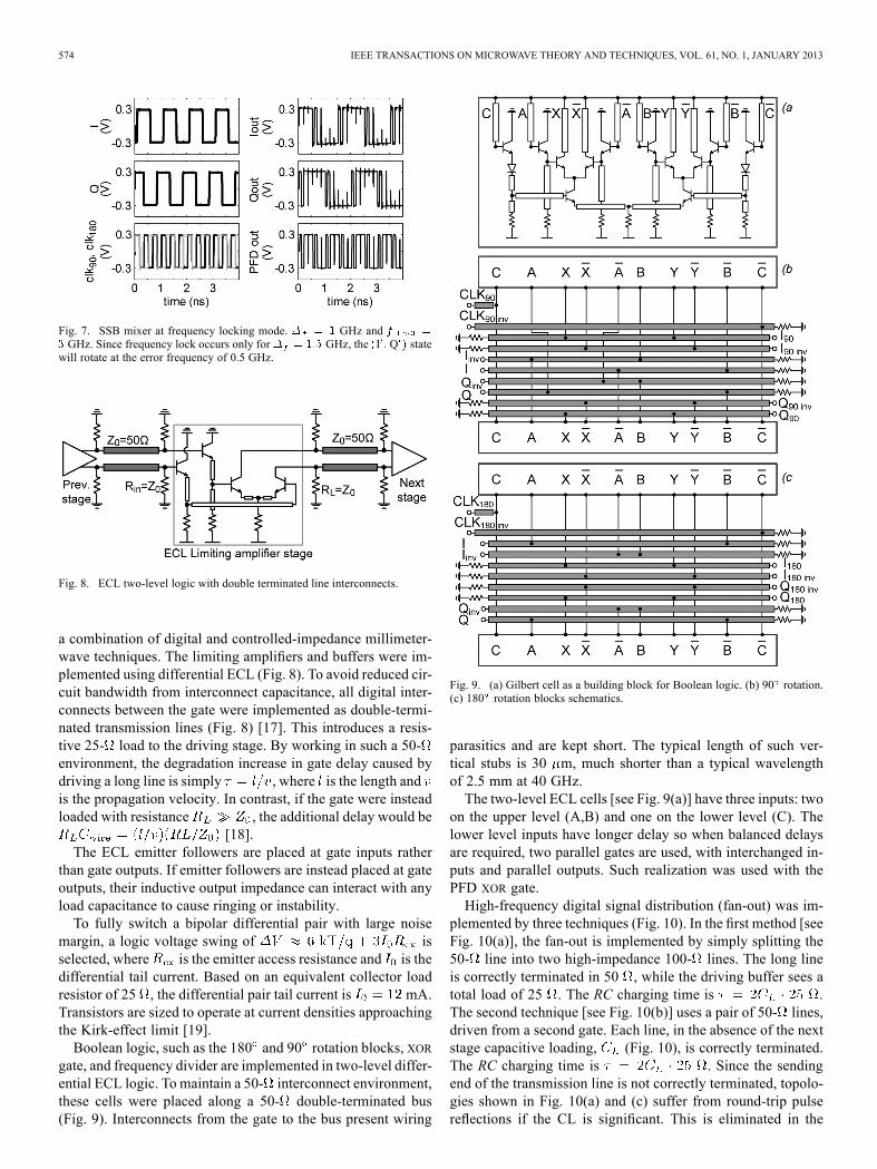
Fig. 4. Digitally limited I/Q signals for optical frequency offset. (a) Time-do-main square wave. (b) Rotating constellation in the (I,Q) plane.
Fig. 5. Digital state rotation. (a) 180 rotation. (b) 90 rotation. (c) 270 rota-tion.
plifier gains. In this circumstance, precise control of the PLLbandwidth would have been difficult to obtain.Subsequent to digital limiting, frequency shifts are introduced
with a digital SSB mixer (Fig. 3). Given a positive laser fre-quency offset , the I/Q photocurrents rotate counterclock-wise through the points (1,1), ( 1,1), , (1, 1) in the(I,Q) plane (Fig. 4). For a negative frequency offset, , thisrotation reverses. For zero frequency offset, the constellationremains static at one of the four points as determined by the rel-ative laser phases.The digital SSBmixer provides a frequency offset by rotating
this constellation in the opposing direction, producing a staticoutput pair I Q . The mixer is formed of cascaded 180 and90 rotation blocks. The 180 block rotates the (I,Q) state by180 (i.e., , etc.) when its input clock is 1, butprovides no rotation when its input clock is 0. The 90 block ro-tates the (I,Q) state by 90 (i.e., , etc.) when itsinput clock is 1, but provides no rotation when its input clock is0. Applying high clock signals to both blocks rotates the state by270 (Fig. 5). Applying periodically clock signals ,at a 2:1 frequency ratio to the 180 and 90 rotation blocks ro-tates the I Q constellation and provides frequency shifts ;these signals are derived from a static frequency divider [16],(Fig. 3). Inverting the sign of , by changing the rotationcontrol signal, inverts the rotation direction, and therefore, thesign of the frequency offset.The PFD is an emitter-coupled logic (ECL) XOR gate with
a delay line of 10 ps in the Q arm. This frequency detector
Fig. 6. SSB mixer at phase detection mode. Signal propagation as a functionof various I/Q phases relative to . For 45 phase, a 50% duty cycle outputsignal with zero average dc.
permits automatic loop acquisition for offset frequencies below50 GHz. To force equal transistor delays on both inputs, the
gate uses two parallel multipliers with crossed inputs and shuntoutputs. The small-signal analysis of the PFD is developed in(7).In the phase-locked mode, i.e., when the laser offset, ,
matches the frequency (i.e., ) under a suit-able rotation control sign, the relative phase between the laserswill change the I/Q signals phase relative to and .This will eventually result in the I Q state oscillating at a fre-quency between two adjacent states (A and B, B and C,etc.) with a duty cycle determined by the phase offset (Fig. 6). Inthis operation mode, either I or Q is constant, while the othersignal oscillates between 1 and 0 at a frequency of with aduty cycle varying linearly with the phase offset. In this mode,the output of the XOR gate is a similar oscillating digital signal.For a 45 (I,Q) phase relative to , the oscillation has 50%duty cycle; hence, the PFD provides zero dc (average) output.This brings the system into lock. Since the PFD output is dig-ital with only its pulse duty cycle varying as a function of loopphase offset, there is no dependence on the photocurrent mag-nitudes of the circuit’s parameters.In PLL frequency acquisition mode, which occurs when the
frequency offset between the reference and the offset laserdoes not match the frequency (i.e., ), the Iand Q outputs are quadrature square waves whose frequencyis error frequency (Fig. 7). Since the PFD output is formed byforming the XOR product of these signals after introducing arelative delay , the PFD output has a dc component varying as
(7). This dc signal forces the RF and LO lasers intofrequency synchronization at the offset frequency , i.e.,forces the loop into lock. The digital frequency-detector gain isindependent of all optical or electronic IC parameters, exceptthat of the delay line , and hence, is well controlled in thepresence of normal optical and IC process parameter variations.
B. High-Frequency Digital Design
The circuit is a complex digital IC operating with digital sig-nals over a dc–40-GHz range. Circuit design and layout required
574 IEEE TRANSACTIONS ON MICROWAVE THEORY AND TECHNIQUES, VOL. 61, NO. 1, JANUARY 2013
Fig. 7. SSB mixer at frequency locking mode. GHz andGHz. Since frequency lock occurs only for GHz, the I Q state
will rotate at the error frequency of 0.5 GHz.
Fig. 8. ECL two-level logic with double terminated line interconnects.
a combination of digital and controlled-impedance millimeter-wave techniques. The limiting amplifiers and buffers were im-plemented using differential ECL (Fig. 8). To avoid reduced cir-cuit bandwidth from interconnect capacitance, all digital inter-connects between the gate were implemented as double-termi-nated transmission lines (Fig. 8) [17]. This introduces a resis-tive 25- load to the driving stage. By working in such a 50-environment, the degradation increase in gate delay caused bydriving a long line is simply , where is the length andis the propagation velocity. In contrast, if the gate were insteadloaded with resistance , the additional delay would be
[18].The ECL emitter followers are placed at gate inputs rather
than gate outputs. If emitter followers are instead placed at gateoutputs, their inductive output impedance can interact with anyload capacitance to cause ringing or instability.To fully switch a bipolar differential pair with large noise
margin, a logic voltage swing of isselected, where is the emitter access resistance and is thedifferential tail current. Based on an equivalent collector loadresistor of 25 , the differential pair tail current is mA.Transistors are sized to operate at current densities approachingthe Kirk-effect limit [19].Boolean logic, such as the 180 and 90 rotation blocks, XOR
gate, and frequency divider are implemented in two-level differ-ential ECL logic. To maintain a 50- interconnect environment,these cells were placed along a 50- double-terminated bus(Fig. 9). Interconnects from the gate to the bus present wiring
Fig. 9. (a) Gilbert cell as a building block for Boolean logic. (b) 90 rotation.(c) 180 rotation blocks schematics.
parasitics and are kept short. The typical length of such ver-tical stubs is 30 m, much shorter than a typical wavelengthof 2.5 mm at 40 GHz.The two-level ECL cells [see Fig. 9(a)] have three inputs: two
on the upper level (A,B) and one on the lower level (C). Thelower level inputs have longer delay so when balanced delaysare required, two parallel gates are used, with interchanged in-puts and parallel outputs. Such realization was used with thePFD XOR gate.High-frequency digital signal distribution (fan-out) was im-
plemented by three techniques (Fig. 10). In the first method [seeFig. 10(a)], the fan-out is implemented by simply splitting the50- line into two high-impedance 100- lines. The long lineis correctly terminated in 50 , while the driving buffer sees atotal load of 25 . The RC charging time is .The second technique [see Fig. 10(b)] uses a pair of 50- lines,driven from a second gate. Each line, in the absence of the nextstage capacitive loading, (Fig. 10), is correctly terminated.The RC charging time is . Since the sendingend of the transmission line is not correctly terminated, topolo-gies shown in Fig. 10(a) and (c) suffer from round-trip pulsereflections if the CL is significant. This is eliminated in the
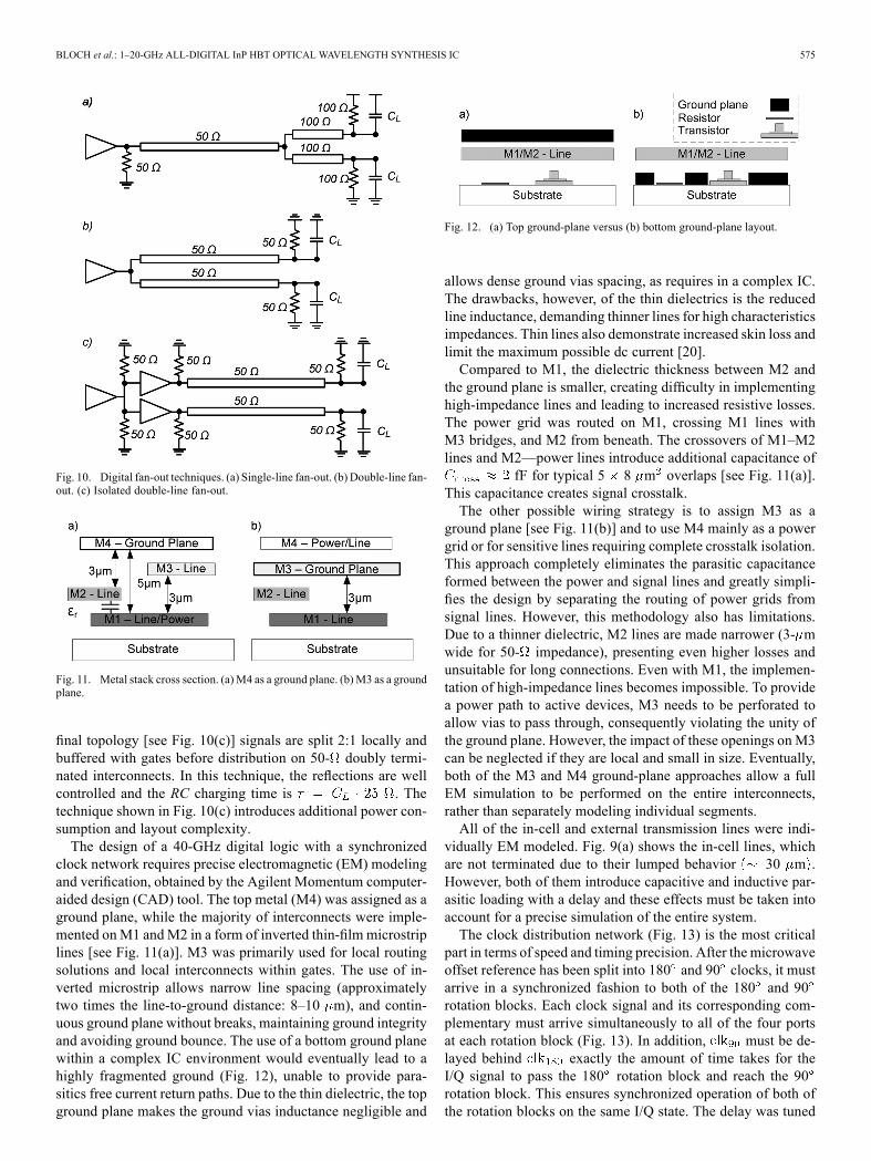
BLOCH et al.: 1–20-GHz ALL-DIGITAL InP HBT OPTICAL WAVELENGTH SYNTHESIS IC 575
Fig. 10. Digital fan-out techniques. (a) Single-line fan-out. (b) Double-line fan-out. (c) Isolated double-line fan-out.
Fig. 11. Metal stack cross section. (a)M4 as a ground plane. (b)M3 as a groundplane.
final topology [see Fig. 10(c)] signals are split 2:1 locally andbuffered with gates before distribution on 50- doubly termi-nated interconnects. In this technique, the reflections are wellcontrolled and the RC charging time is . Thetechnique shown in Fig. 10(c) introduces additional power con-sumption and layout complexity.The design of a 40-GHz digital logic with a synchronized
clock network requires precise electromagnetic (EM) modelingand verification, obtained by the Agilent Momentum computer-aided design (CAD) tool. The top metal (M4) was assigned as aground plane, while the majority of interconnects were imple-mented onM1 andM2 in a form of inverted thin-film microstriplines [see Fig. 11(a)]. M3 was primarily used for local routingsolutions and local interconnects within gates. The use of in-verted microstrip allows narrow line spacing (approximatelytwo times the line-to-ground distance: 8–10 m), and contin-uous ground plane without breaks, maintaining ground integrityand avoiding ground bounce. The use of a bottom ground planewithin a complex IC environment would eventually lead to ahighly fragmented ground (Fig. 12), unable to provide para-sitics free current return paths. Due to the thin dielectric, the topground plane makes the ground vias inductance negligible and
Fig. 12. (a) Top ground-plane versus (b) bottom ground-plane layout.
allows dense ground vias spacing, as requires in a complex IC.The drawbacks, however, of the thin dielectrics is the reducedline inductance, demanding thinner lines for high characteristicsimpedances. Thin lines also demonstrate increased skin loss andlimit the maximum possible dc current [20].Compared to M1, the dielectric thickness between M2 and
the ground plane is smaller, creating difficulty in implementinghigh-impedance lines and leading to increased resistive losses.The power grid was routed on M1, crossing M1 lines withM3 bridges, and M2 from beneath. The crossovers of M1–M2lines and M2—power lines introduce additional capacitance of
fF for typical 5 8 m overlaps [see Fig. 11(a)].This capacitance creates signal crosstalk.The other possible wiring strategy is to assign M3 as a
ground plane [see Fig. 11(b)] and to use M4 mainly as a powergrid or for sensitive lines requiring complete crosstalk isolation.This approach completely eliminates the parasitic capacitanceformed between the power and signal lines and greatly simpli-fies the design by separating the routing of power grids fromsignal lines. However, this methodology also has limitations.Due to a thinner dielectric, M2 lines are made narrower (3- mwide for 50- impedance), presenting even higher losses andunsuitable for long connections. Even with M1, the implemen-tation of high-impedance lines becomes impossible. To providea power path to active devices, M3 needs to be perforated toallow vias to pass through, consequently violating the unity ofthe ground plane. However, the impact of these openings on M3can be neglected if they are local and small in size. Eventually,both of the M3 and M4 ground-plane approaches allow a fullEM simulation to be performed on the entire interconnects,rather than separately modeling individual segments.All of the in-cell and external transmission lines were indi-
vidually EM modeled. Fig. 9(a) shows the in-cell lines, whichare not terminated due to their lumped behavior 30 m .However, both of them introduce capacitive and inductive par-asitic loading with a delay and these effects must be taken intoaccount for a precise simulation of the entire system.The clock distribution network (Fig. 13) is the most critical
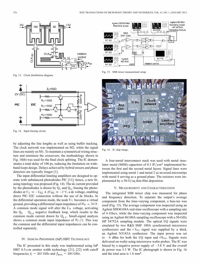
part in terms of speed and timing precision. After the microwaveoffset reference has been split into 180 and 90 clocks, it mustarrive in a synchronized fashion to both of the 180 and 90rotation blocks. Each clock signal and its corresponding com-plementary must arrive simultaneously to all of the four portsat each rotation block (Fig. 13). In addition, must be de-layed behind exactly the amount of time takes for theI/Q signal to pass the 180 rotation block and reach the 90rotation block. This ensures synchronized operation of both ofthe rotation blocks on the same I/Q state. The delay was tuned
576 IEEE TRANSACTIONS ON MICROWAVE THEORY AND TECHNIQUES, VOL. 61, NO. 1, JANUARY 2013
Fig. 13. Clock distribution diagram.
Fig. 14. Input biasing circuit.
by adjusting the line lengths as well as using buffer stacking.The clock network was implemented on M2, while the signallines are mainly onM1. Tomaintain a symmetrical wiring struc-ture and minimize the crossovers, the methodology shown inFig. 10(b) was used for the final clock splitting. The IC demon-strates a total delay of 100 ps, reducing the limitation on wide-band loops design. Delays achieved by hybrid mixers and phasedetectors are typically longer [1].The input differential limiting amplifiers are designed to op-
erate with unbalanced photodiodes PIC [11]; hence, a new bi-asing topology was proposed (Fig. 14). The dc current providedby the photodiodes is drawn by Q and Q , biasing the photo-diodes at V, a dc voltage, enablingdirect PIC–EIC connection without the use of dc blocks. Inthe differential operation mode, the node becomes a virtualground, providing a differential input impedance of .A common mode signal will alter the voltage, activatingthe Q Q negative feedback loop, which results in thecommon mode current drawn by Q . Small-signal analysisshows a common mode input impedance of . This waythe common and the differential input impedances can be con-trolled separately.
IV. INDIUM–PHOSPHIDE (InP) HBT TECHNOLOGY
The IC presented in this study was implemented using InPHBT 0.5- m emitter width technology [21], [22] with cutofffrequencies GHz and GHz.
Fig. 15. SSB mixer measurement setup.
Fig. 16. IC chip image.
A four-metal interconnect stack was used with metal–insu-lator–metal (MIM) capacitors of 0.3 fF m implemented be-tween the first and the second metal layers. Signal lines wereimplemented using metal 1 and metal 2 as inversed microstripswith metal 4 serving as a ground plane. The resistors were im-plemented by a 50- sq thin-film deposition.
V. MEASUREMENT AND CHARACTERIZATION
The integrated SSB mixer chip was measured for phaseand frequency detection. To separate the output’s averagecomponent from the time-varying component, a bias-tee wasused (Fig. 15). The average component was inspected using anAgilent SDO6104A real-time oscilloscope with a sampling rateof 4 GSa/s, while the time-varying component was inspectedusing an Agilent 86100A sampling oscilloscope with a 50-GHzHP 54752A sampling module. The optical I/Q signals wereemulated by two R&S SMF 100A synchronized microwavesynthesizers and the signal was supplied by a third,an Agilent N5183A synthesizer. The input power was setto 4 dBm for both the I/Q input and . Signals weredelivered on-wafer using microwave wafer probes. The IC wasbiased by a negative power supply of 3.8 V and the overalldc power was 5.3 W. The IC photograph is shown in Fig. 16and the total area is 1.8 mm .
BLOCH et al.: 1–20-GHz ALL-DIGITAL InP HBT OPTICAL WAVELENGTH SYNTHESIS IC 577
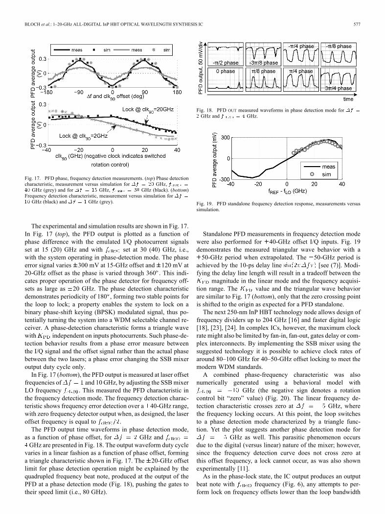
Fig. 17. PFD phase, frequency detection measurements. (top) Phase detectioncharacteristic, measurement versus simulation for GHz,GHz (grey) and for GHz, GHz (black). (bottom)
Frequency detection characteristic, measurement versus simulation forGHz (black) and GHz (grey).
The experimental and simulation results are shown in Fig. 17.In Fig. 17 (top), the PFD output is plotted as a function ofphase difference with the emulated I/Q photocurrent signalsset at 15 (20) GHz and with set at 30 (40) GHz, i.e.,with the system operating in phase-detection mode. The phaseerror signal varies 300 mV at 15-GHz offset and 120 mV at20-GHz offset as the phase is varied through 360 . This indi-cates proper operation of the phase detector for frequency off-sets as large as 20 GHz. The phase detection characteristicdemonstrates periodicity of 180 , forming two stable points forthe loop to lock; a property enables the system to lock on abinary phase-shift keying (BPSK) modulated signal, thus po-tentially turning the system into a WDM selectable channel re-ceiver. A phase-detection characteristic forms a triangle wavewith independent on inputs photocurrents. Such phase-de-tection behavior results from a phase error measure betweenthe I/Q signal and the offset signal rather than the actual phasebetween the two lasers; a phase error changing the SSB mixeroutput duty cycle only.In Fig. 17 (bottom), the PFD output is measured at laser offset
frequencies of and 10 GHz, by adjusting the SSBmixerLO frequency . This measured the PFD characteristic inthe frequency detection mode. The frequency detection charac-teristic shows frequency error detection over a 40-GHz range,with zero frequency detector output when, as designed, the laseroffset frequency is equal to .The PFD output time waveforms in phase detection mode,
as a function of phase offset, for GHz andGHz are presented in Fig. 18. The output waveform duty cyclevaries in a linear fashion as a function of phase offset, forminga triangle characteristic shown in Fig. 17. The 20-GHz offsetlimit for phase detection operation might be explained by thequadrupled frequency beat note, produced at the output of thePFD at a phase detection mode (Fig. 18), pushing the gates totheir speed limit (i.e., 80 GHz).
Fig. 18. PFD OUT measured waveforms in phase detection mode forGHz and GHz.
Fig. 19. PFD standalone frequency detection response, measurements versussimulation.
Standalone PFD measurements in frequency detection modewere also performed for 40-GHz offset I/Q inputs. Fig. 19demonstrates the measured triangular wave behavior with a50-GHz period when extrapolated. The 50-GHz period is
achieved by the 10-ps delay line [see (7)]. Modi-fying the delay line length will result in a tradeoff between the
magnitude in the linear mode and the frequency acquisi-tion range. The value and the triangular wave behaviorare similar to Fig. 17 (bottom), only that the zero crossing pointis shifted to the origin as expected for a PFD standalone.The next 250-nm InP HBT technology node allows design of
frequency dividers up to 204 GHz [16] and faster digital logic[18], [23], [24]. In complex ICs, however, the maximum clockrate might also be limited by fan-in, fan-out, gates delay or com-plex interconnects. By implementing the SSB mixer using thesuggested technology it is possible to achieve clock rates ofaround 80–100 GHz for 40–50-GHz offset locking to meet themodern WDM standards.A combined phase-frequency characteristic was also
numerically generated using a behavioral model withGHz (the negative sign denotes a rotation
control bit “zero” value) (Fig. 20). The linear frequency de-tection characteristic crosses zero at GHz, wherethe frequency locking occurs. At this point, the loop switchesto a phase detection mode characterized by a triangle func-tion. Yet the plot suggests another phase detection mode for
GHz as well. This parasitic phenomenon occursdue to the digital (versus linear) nature of the mixer; however,since the frequency detection curve does not cross zero atthis offset frequency, a lock cannot occur, as was also shownexperimentally [11].As in the phase-lock state, the IC output produces an output
beat note with frequency (Fig. 6), any attempts to per-form lock on frequency offsets lower than the loop bandwidth
578 IEEE TRANSACTIONS ON MICROWAVE THEORY AND TECHNIQUES, VOL. 61, NO. 1, JANUARY 2013
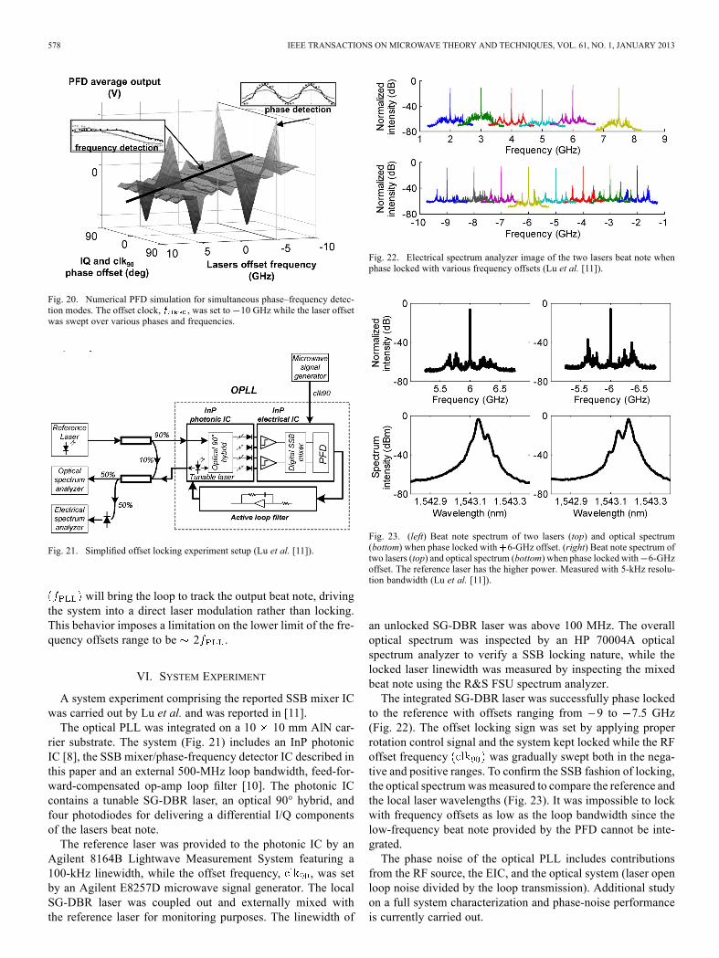
Fig. 20. Numerical PFD simulation for simultaneous phase–frequency detec-tion modes. The offset clock, , was set to 10 GHz while the laser offsetwas swept over various phases and frequencies.
Fig. 21. Simplified offset locking experiment setup (Lu et al. [11]).
will bring the loop to track the output beat note, drivingthe system into a direct laser modulation rather than locking.This behavior imposes a limitation on the lower limit of the fre-quency offsets range to be 2 .
VI. SYSTEM EXPERIMENT
A system experiment comprising the reported SSB mixer ICwas carried out by Lu et al. and was reported in [11].The optical PLL was integrated on a 10 10 mm AlN car-
rier substrate. The system (Fig. 21) includes an InP photonicIC [8], the SSB mixer/phase-frequency detector IC described inthis paper and an external 500-MHz loop bandwidth, feed-for-ward-compensated op-amp loop filter [10]. The photonic ICcontains a tunable SG-DBR laser, an optical 90° hybrid, andfour photodiodes for delivering a differential I/Q componentsof the lasers beat note.The reference laser was provided to the photonic IC by an
Agilent 8164B Lightwave Measurement System featuring a100-kHz linewidth, while the offset frequency, , was setby an Agilent E8257D microwave signal generator. The localSG-DBR laser was coupled out and externally mixed withthe reference laser for monitoring purposes. The linewidth of
Fig. 22. Electrical spectrum analyzer image of the two lasers beat note whenphase locked with various frequency offsets (Lu et al. [11]).
Fig. 23. (left) Beat note spectrum of two lasers (top) and optical spectrum(bottom) when phase locked with 6-GHz offset. (right) Beat note spectrum oftwo lasers (top) and optical spectrum (bottom) when phase locked with 6-GHzoffset. The reference laser has the higher power. Measured with 5-kHz resolu-tion bandwidth (Lu et al. [11]).
an unlocked SG-DBR laser was above 100 MHz. The overalloptical spectrum was inspected by an HP 70004A opticalspectrum analyzer to verify a SSB locking nature, while thelocked laser linewidth was measured by inspecting the mixedbeat note using the R&S FSU spectrum analyzer.The integrated SG-DBR laser was successfully phase locked
to the reference with offsets ranging from 9 to 7.5 GHz(Fig. 22). The offset locking sign was set by applying properrotation control signal and the system kept locked while the RFoffset frequency was gradually swept both in the nega-tive and positive ranges. To confirm the SSB fashion of locking,the optical spectrumwasmeasured to compare the reference andthe local laser wavelengths (Fig. 23). It was impossible to lockwith frequency offsets as low as the loop bandwidth since thelow-frequency beat note provided by the PFD cannot be inte-grated.The phase noise of the optical PLL includes contributions
from the RF source, the EIC, and the optical system (laser openloop noise divided by the loop transmission). Additional studyon a full system characterization and phase-noise performanceis currently carried out.
BLOCH et al.: 1–20-GHz ALL-DIGITAL InP HBT OPTICAL WAVELENGTH SYNTHESIS IC 579
VII. CONCLUSION
We have demonstrated a novel broadband 20-GHz opticalfrequency synthesis IC in 0.5- m InP HBT technology. Theall-digital mixer topology eliminates the dependency on inputphotocurrent, increases the offset locking range, and improvesthe design robustness by shifting to a digital domain. The ICis comprised of a SSB mixer and a Quadricorrelator PFD withfrequency acquisition range up to 40 GHz. A full integrationof the mixer with the PFD drastically reduces the limitation onloop delay, making larger loop bandwidths possible.
ACKNOWLEDGMENT
The authors would like to thank Teledyne Scientific andImaging, Thousand Oaks, CA, for MMIC fabrication.
REFERENCES
[1] R. J. Steed, L. Ponnampalam, M. J. Fice, C. C. Renaud, D. C. Rogers,D. G. Moodie, G. D. Maxwell, I. F. Lealman, M. J. Robertson, L.Pavlovic, L. Naglic, M. Vidmar, and A. J. Seeds, “Hybrid integratedoptical phase-lock loops for photonic terahertz sources,” IEEE J. Sel.Top. Quantum Electron., vol. 17, no. 1, pp. 210–217, Jan.–Feb. 2011.
[2] R. J. Steed, F. Pozzi, M. J. Fice, C. C. Renaud, D. C. Rogers, I. F.Lealman, D. G. Moodie, P. J. Cannard, C. Lynch, L. Johnston, M. J.Robertson, R. Cronin, L. Pavlovic, L. Naglic, M. Vidmar, and A. J.Seeds, “Monolithically integrated heterodyne optical phase-lock loopwith RF XOR phase detector,” Opt. Exp., vol. 19, Sep. 2011, Art. ID20048.
[3] M. Grant, W. Michie, and M. Fletcher, “The performance of opticalphase-locked loops in the presence of nonnegligible loop propagationdelay,” J. Lightw. Technol., vol. JLT-5, no. 4, pp. 592–597, Apr. 1987.
[4] U. Gliese, T. N. Nielsen, M. Bruun, E. Lintz Christensen, K. E. Stubk-jaer, S. Lindgren, and B. Broberg, “A wideband heterodyne opticalphase-locked loop for generation of 3–18 GHz microwave carriers,”IEEE Photon. Technol. Lett., vol. 4, no. 8, pp. 936–938, Aug. 1992.
[5] L. N. Langley, M. D. Elkin, C. Edge, M. J. Wale, U. Gliese, X. Huang,and A. J. Seeds, “Packaged semiconductor laser optical phase-lockedloop (OPLL) for photonic generation, processing and transmission ofmicrowave signals,” IEEE Trans. Microw. Theory Techn. , vol. 47, no.7, pp. 1257–1264, Jul. 1999.
[6] S. Ristic, A. Bhardwaj, M. J. Rodwell, L. A. Coldren, and L. A. Jo-hansson, “An optical phase-locked loop photonic integrated circuit,”J. Lightw. Technol., vol. 28, no. 4, pp. 526–538, Feb. 2010.
[7] Z. F. Fan, P. J. S. Heim, and M. Dagenais, “Highly coherent RF signalgeneration by heterodyne optical phase locking of external cavitysemiconductor lasers,” IEEE Photon. Technol. Lett., vol. 10, no. 5, pp.719–721, May 1998.
[8] M. Lu, A. Bhardwaj, A. Sivananthan, L. A. Johansson, H. Park, E.Bloch, M. J. Rodwell, and L. A. Coldren, “A widely-tunable integratedcoherent optical receiver using a phase-locked loop,” in IEEE Photon.Conf., 2011, pp. 769–770.
[9] E. Bloch, H. Park, M. Lu, T. Reed, Z. Griffith, L. A. Johansson, L. A.Coldren, D. Ritter, and M. J. Rodwell, “A 1–20 GHz InP HBT phase-lock-loop IC for optical wavelength synthesis,” in IEEE MTT-S Int.Microw. Symp. Dig., 2012, pp. 1–3.
[10] H. Park, M. Lu, E. Bloch, T. Reed, Z. Griffith, L. Johansson, L. Col-dren, and M. Rodwell, “40 Gbit/s coherent optical receiver using acostas loop,” in Eur. Opt. Commun. Conf., Amsterdam, The Nether-lands, 2012, Paper Th.3.A.2.
[11] M. Lu, H. Park, E. Bloch, A. Sivananthan, A. Bhardwaj, Z. Griffith,L. A. Johansson, M. J. Rodwell, and L. A. Coldren, “Highly integratedoptical heterodyne phase-locked loop with phase/frequency detection,”Opt. Exp., vol. 20, pp. 9736–9741, Apr. 2012.
[12] B. Razavi, Monolithic Phase-Locked Loops and Clock Recovery Cir-cuits: Theory and Design. Piscataway, NJ: IEEE Press, 1996.
[13] F. M. Gardner, Phaselock Techniques. New York: Wiley, 1979.
[14] F. Gardner, “Properties of frequency difference detectors,” IEEE Trans.Commun., vol. COM-33, no. 2, pp. 131–138, Feb. 1985.
[15] D. K. Weaver, “A third method of generation and detection of single-sideband signals,” Proc. IRE, vol. 44, no. 12, pp. 1703–1705, Dec.1956.
[16] Z. Griffith, M. Urteaga, R. Pierson, P. Rowell, M. Rodwell, and B.Brar, “A 204.8 GHz static divide-by-8 frequency divider in 250 nmInP HBT,” in IEEE Compound Semicond. Integr. Circuit Symp., 2010,pp. 1–4.
[17] Y. Betser, S. Jaganathan, T. Mathew, Q. Lee, J. Guthrie, D. Mensa, andM. J. W. Rodwell, “Low voltage swing techniques for 100 GHz logic,”in Int. Infrared Millim. Waves Conf. , Monterey, CA, 1999.
[18] Z. Griffith, Y. Dong, D. Scott, Y.Wei, N. Parthasarathy, M. Dahlstrom,C. Kadow, V. Paidi, M. J. W. Rodwell, M. Urteaga, R. Pierson, P.Rowell, B. Brar, S. Lee, N. X. Nguyen, and C. Nguyen, “Transistorand circuit design for 100–200-GHz ICs,” IEEE J. Solid-State Circuits,vol. 40, no. 10, pp. 2061–2069, Oct. 2005.
[19] M. Urteaga, S. Krishnan, D. Scott, Y. Wei, M. Dahlstrom, S. Lee,and M. J. W. Rodwell, “Submicron InP-based HBTs for ultrahighfrequency amplifiers,” Int. J. High Speed Electron. Syst., vol. 13, pp.457–495, 2003.
[20] M. J. W. Rodwell, S. Krishnan, M. Urteaga, Z. Griffith, M. Dahlstrom,Y. Wei, D. Scott, N. Parthasarathy, Y. Kim, and S. Lee, “Interconnectsin 50–100 GHz integrated circuits,” in Int. Union Radio Sci., Maas-tricht, The Netherlands, 2002.
[21] M. Urteaga, R. Pierson, P. Rowell, M. Choe, D. Mensa, and B. Brar,“Advanced InP DHBT process for high speed LSI circuits,” in 20th Int.Indium Phosphide and Rel. Mater. Conf., 2008, pp. 1–5.
[22] M. Rodwell, E. Lind, Z. Griffith, A. M. Crook, S. R. Bank, U.Singisetti, M. Wistey, G. Burek, and A. C. Gossard, “On the feasibilityof few-THz bipolar transistors,” in IEEE Bipolar/BiCMOS CircuitsTechnol. Meeting, 2007, pp. 17–21.
[23] Z. Griffith, M. Dahlstrom, M. J. W. Rodwell, X.-. Fang, D. Luby-shev, Y. Wu, J. M. Fastenau, and W. K. Liu, “InGaAs-InP DHBTs forincreased digital IC bandwidth having a 391-GHz and 505-GHz
,” IEEE Electron Device Lett., vol. 26, no. 1, pp. 11–13, Jan.2005.
[24] M. Rodwell, Z. Griffith, V. Paidi, N. Parthasarathy, C. Sheldon, U.Singisetti, M. Urteaga, R. Pierson, P. Rowell, and B. Brar, “InP HBTdigital ICs and MMICs in the 140–220 GHz band,” in Joint 30th Int.Infrared Millim. Waves Conf. and 13th Int. Terahertz Electron. Conf.,2005, vol. 2, pp. 620–621.
Eli Bloch received the B.Sc. and M.Sc. degrees inelectrical engineering from the Technion–Israel Insti-tute of Technology (IIT), Haifa, Israel, in 2006 and2010, respectively, and is currently working towardthe Ph.D degree in electrical engineering at the Tech-nion–IIT.From 2005 to 2007 he was with the Research
and Development Laboratories, IBM, Haifa, Is-rael, where he was involved with analog andmixed-signal circuit design. His current researchfocuses on millimeer-wave and mixed-signal ICs,
based on InP/GaInAs HBTs, for optical coherent communication and opticalphase locking.
Hyunchul Park received the B.S. and the M.Sdegrees in electrical and computer engineering fromSungkyunkwan University, Suwon, Korea, in 2006and 2008, respectively, and is currently workingtoward the Ph.D. degree in electrical and computerengineering at the University of California at SantaBarbara.His past research interests include high-efficiency
and power-amplifier designs. He is currently focusedon high-speed IC designs for optical links and mi-crowave/millimeter-wave communication systems.
580 IEEE TRANSACTIONS ON MICROWAVE THEORY AND TECHNIQUES, VOL. 61, NO. 1, JANUARY 2013
Mingzhi Lu received the B.S. degree in electrical en-gineering from Southeast University, Nanjing, China,in 2008, and is currently working toward the Ph.D.degree in electrical engineering at the University ofCalifornia at Santa Barbara.His past research experience includes microwave
and terahertz frequency-selective surfaces (FSSs)and metamaterials. He is currently focused onInGaAsP/InP-based photonic integrated coherentreceivers and the optical PLL.
Thomas Reed (M’08) received the B.S. degree inelectrical engineering from Brigham Young Univer-sity, Provo, UT, in 2008, the M.S. degree in electricalengineering degree from the University of Californiaat Santa Barbara (UCSB), in 2009, and is currentlyworking toward the Ph.D. degree in electrical engi-neering at UCSB.Since 2008, he has been a member of the High
Frequency Electronics Group, UCSB. His researchfocuses on solid-state power amplifier and RFIC design using nanoscale HBT technologies at
millimeter-wave and sub-millimeter-wave frequencies.
Zach Griffith received the Ph.D. degree in elec-trical engineering from the University of Californiaat Santa Barbara, in 2005. His doctoral researchconcerned the development of record bandwidth InPHBTs.Since joining Teledyne Scientific and Imaging,
Thousand Oaks, CA, in 2008, his efforts are focusedon designing millimeter-wave op-amps for highlylinear ( 55 dBm OIP3), low-gigahertz amplificationwith low Pdc, as well as high millimeter-wave,sub-millimeter-wave power amplifiers. He has
authored or coauthored over 75 publications across these fields.
Leif A. Johansson (M’04) received the Ph.D. de-gree in engineering from University College London,London, U.K., in 2002.He is currently a Research Scientist with the Uni-
versity of California at Santa Barbara. His current re-search interests include design and characterizationof integrated photonic devices for analog and digitalapplications and analog photonic systems and sub-systems.
Larry A. Coldren (S’67–M’72–SM’77–F’82–LF’12) received the Ph.D. degree in electricalengineering from Stanford University, Stanford, CA.He is currently the Fred Kavli Professor of
Optoelectronics and Sensors with the Universityof California at Santa Barbara (UCSB). He spent13 years in research with Bell Laboratories priorto joining UCSB, in 1984, where he holds appoint-ments in electrical and computer engineering andmaterials. He cofounded Optical Concepts (acquiredas Gore Photonics), to develop novel vertical-cavity
surface-emitting laser (VCSEL) technology, and later Agility Communications(acquired by JDSU), to develop widely tunable integrated transmitters. WithBell Laboratories, he was involved with surface acoustic wave (SAW) filtersand tunable coupled-cavity lasers using novel reactive ion etching (RIE) tech-nology. With UCSB, he has continued his involvedment on multiple-sectionlasers, in 1988 inventing the widely tunable multielement mirror concept thatis now used in numerous commercial products. He has also made seminalcontributions to efficient VCSEL designs. His group continues efforts onhigh-performance InP-based PICs and high-speed VCSELs. He has authoredor coauthored over 1000 journal and conference papers, a number of bookchapters, and a textbook. He holds 64 patents.Dr. coldren is a Fellow of Optical Society of America (OSA) and the Insti-
tution of Electrical Engineers (IEE). He is a member of the National Academyof Engineering. He was a recipient of the 2004 John Tyndall Award and 2009Aron Kressel Award.
Dan Ritter received the B.Sc., M.Sc., and Ph.D. de-grees in electrical engineering from the Technion–Is-rael Institute of Technology (IIT), Haifa, Israel, in1979, 1982, and 1988, respectively.From 1988 to 1992, he performed postdoctoral
research with AT&T Bell Laboratories, Murray Hill,NJ. In 1992, he joined the Department of ElectricalEngineering, Technion–IIT, where he is currently aProfessor. His fields of research are semiconductorepitaxial crystal growth, compound semiconductordevices, and high-speed circuits.
Mark Rodwell (M’89–SM’99–F’03) recieved thePh.D. degree from Stanford University, Stanford,CA, in 1988.He holds the Doluca Family Endowed Chair
in Electrical and Computer Engineering with theUniversity of California at Santa Barbara (UCSB).He directs the UCSB node of the National ScienceFoundation (NSF) Nanofabrication InfrastructureNetwork (NNIN), and the SRC Nonclassical CMOSResearch Center. His research group works toextend the operation of ICs to the highest feasible
frequencies.Prof. Rodwell was the recipient of the 2010 IEEE Sarnoff Award and the
2009 IEEE IPRM Conference Award for the development of InP-based bipolarIC technology, at both device and circuit design level, for millimeter-wave andsub-millimeter-wave applications. His group’s work on GaAs Schottky-diodeICs for subpicosecond/millimeter-wave instrumentation was awarded the 1997IEEE Microwave Prize and the 1998 European Microwave Conference Mi-crowave Prize.