Embed Size (px)
Citation preview
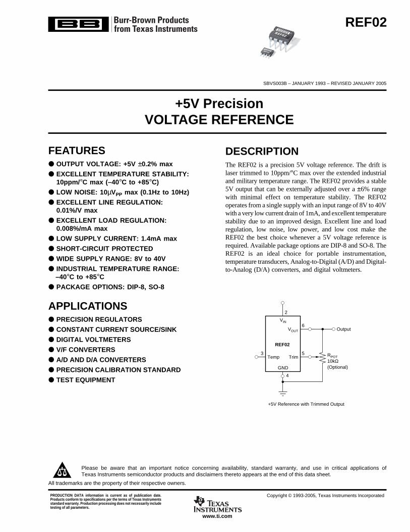
+5V PrecisionVOLTAGE REFERENCE
FEATURES OUTPUT VOLTAGE: +5V ±0.2% max
EXCELLENT TEMPERATURE STABILITY:10ppm/°C max (–40°C to +85°C)
LOW NOISE: 10µVPP max (0.1Hz to 10Hz)
EXCELLENT LINE REGULATION:0.01%/V max
EXCELLENT LOAD REGULATION:0.008%/mA max
LOW SUPPLY CURRENT: 1.4mA max
SHORT-CIRCUIT PROTECTED
WIDE SUPPLY RANGE: 8V to 40V
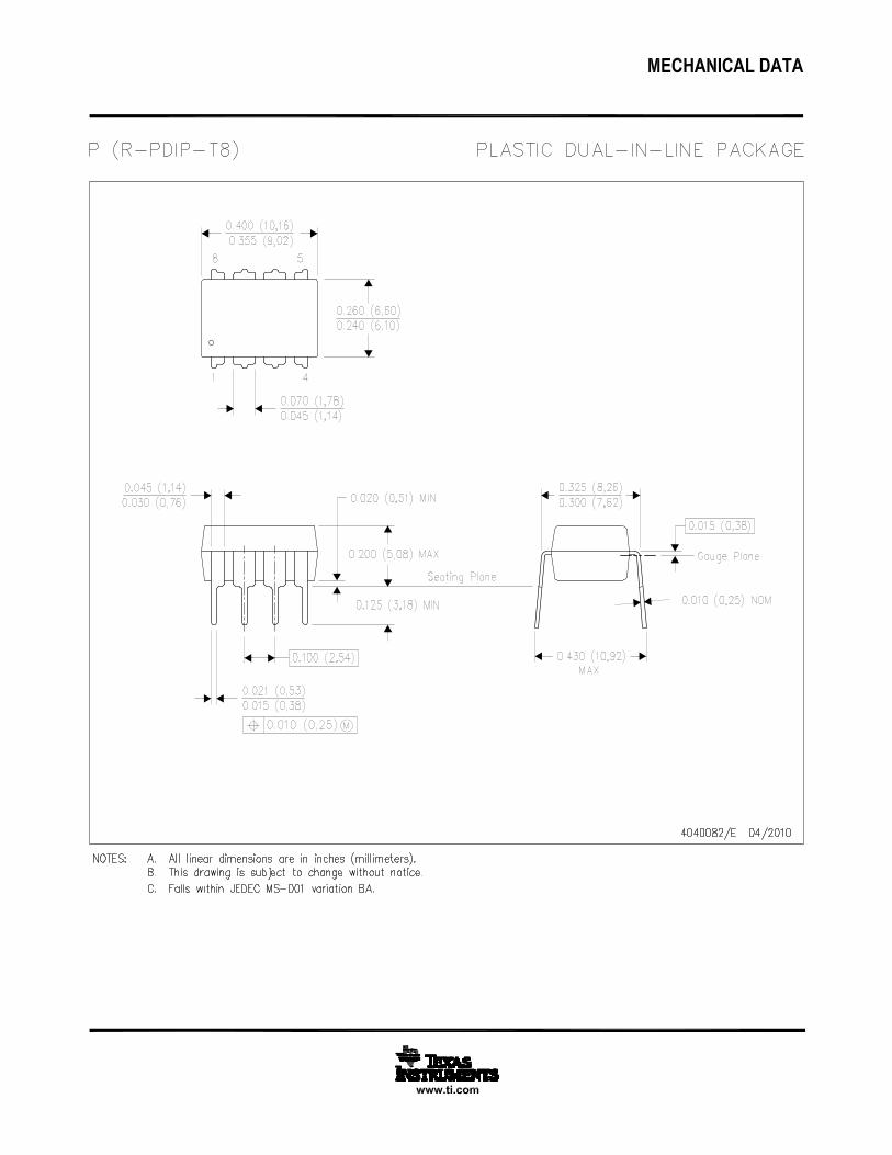
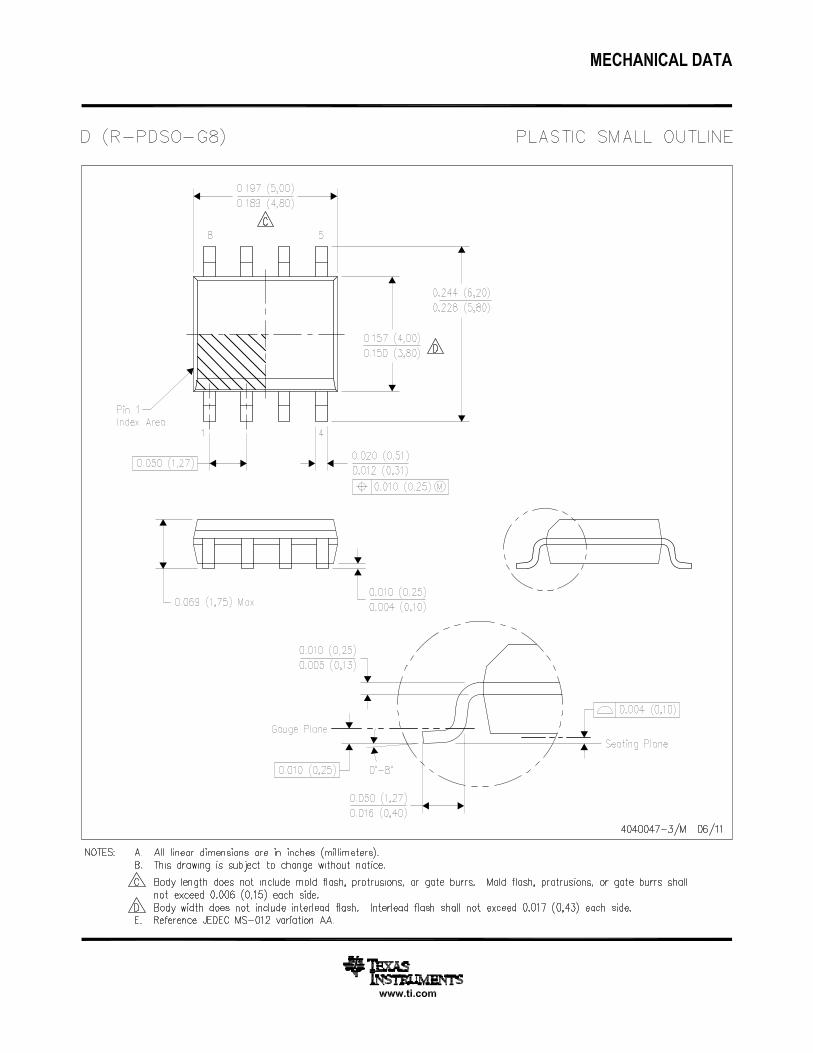
INDUSTRIAL TEMPERATURE RANGE: –40°C to +85°C PACKAGE OPTIONS: DIP-8, SO-8
APPLICATIONS PRECISION REGULATORS
CONSTANT CURRENT SOURCE/SINK
DIGITAL VOLTMETERS
V/F CONVERTERS
A/D AND D/A CONVERTERS
PRECISION CALIBRATION STANDARD
TEST EQUIPMENT
DESCRIPTIONThe REF02 is a precision 5V voltage reference. The drift islaser trimmed to 10ppm/°C max over the extended industrialand military temperature range. The REF02 provides a stable5V output that can be externally adjusted over a ±6% rangewith minimal effect on temperature stability. The REF02operates from a single supply with an input range of 8V to 40Vwith a very low current drain of 1mA, and excellent temperaturestability due to an improved design. Excellent line and loadregulation, low noise, low power, and low cost make theREF02 the best choice whenever a 5V voltage reference isrequired. Available package options are DIP-8 and SO-8. TheREF02 is an ideal choice for portable instrumentation,temperature transducers, Analog-to-Digital (A/D) and Digital-to-Analog (D/A) converters, and digital voltmeters.
VOUT
REF02
VIN
Trim
GND
+5V Reference with Trimmed Output
2
6
5
4
RPOT10kΩ(Optional)
Output
3Temp
REF02
REF02
REF02
SBVS003B – JANUARY 1993 – REVISED JANUARY 2005
www.ti.com
PRODUCTION DATA information is current as of publication date.Products conform to specifications per the terms of Texas Instrumentsstandard warranty. Production processing does not necessarily includetesting of all parameters.
Copyright © 1993-2005, Texas Instruments Incorporated
Please be aware that an important notice concerning availability, standard warranty, and use in critical applications ofTexas Instruments semiconductor products and disclaimers thereto appears at the end of this data sheet.
All trademarks are the property of their respective owners.
REF022SBVS003Bwww.ti.com
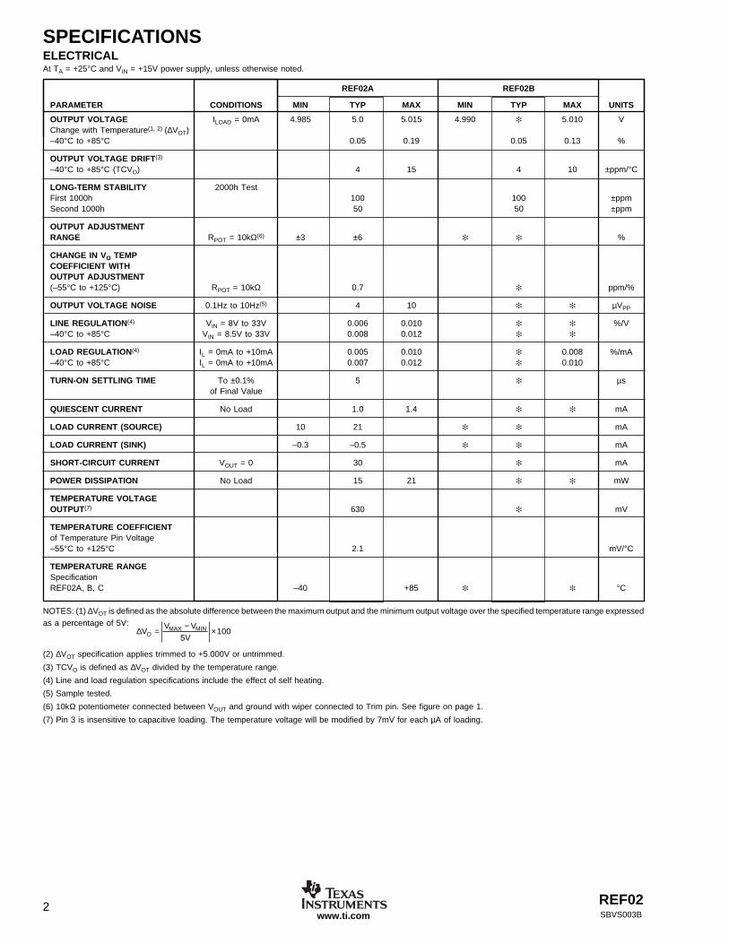
SPECIFICATIONSELECTRICALAt TA = +25°C and VIN = +15V power supply, unless otherwise noted.
REF02A REF02B
PARAMETER CONDITIONS MIN TYP MAX MIN TYP MAX UNITS
OUTPUT VOLTAGE ILOAD = 0mA 4.985 5.0 5.015 4.990 5.010 VChange with Temperature(1, 2) (∆VOT)–40°C to +85°C 0.05 0.19 0.05 0.13 %
OUTPUT VOLTAGE DRIFT(3)
–40°C to +85°C (TCVO) 4 15 4 10 ±ppm/°C
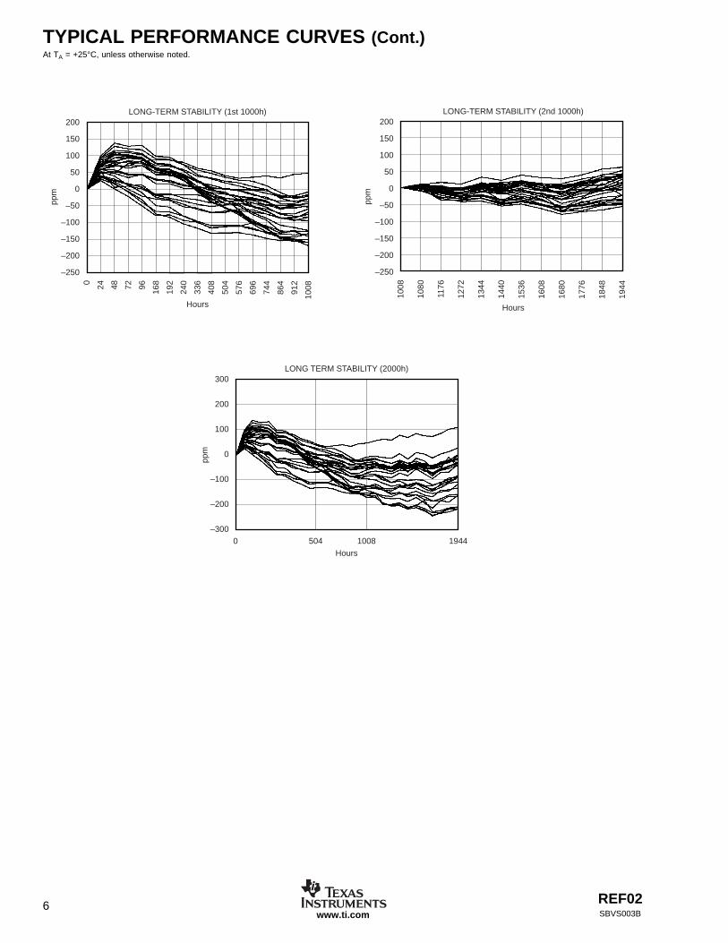
LONG-TERM STABILITY 2000h TestFirst 1000h 100 100 ±ppmSecond 1000h 50 50 ±ppm
OUTPUT ADJUSTMENTRANGE RPOT = 10kΩ(6) ±3 ±6 %
CHANGE IN VO TEMPCOEFFICIENT WITHOUTPUT ADJUSTMENT(–55°C to +125°C) RPOT = 10kΩ 0.7 ppm/%
OUTPUT VOLTAGE NOISE 0.1Hz to 10Hz(5) 4 10 µVPP
LINE REGULATION(4) VIN = 8V to 33V 0.006 0.010 %/V–40°C to +85°C VIN = 8.5V to 33V 0.008 0.012
LOAD REGULATION(4) IL = 0mA to +10mA 0.005 0.010 0.008 %/mA–40°C to +85°C IL = 0mA to +10mA 0.007 0.012 0.010
TURN-ON SETTLING TIME To ±0.1% 5 µsof Final Value
QUIESCENT CURRENT No Load 1.0 1.4 mA
LOAD CURRENT (SOURCE) 10 21 mA
LOAD CURRENT (SINK) –0.3 –0.5 mA
SHORT-CIRCUIT CURRENT VOUT = 0 30 mA
POWER DISSIPATION No Load 15 21 mW
TEMPERATURE VOLTAGEOUTPUT(7) 630 mV
TEMPERATURE COEFFICIENTof Temperature Pin Voltage–55°C to +125°C 2.1 mV/°C
TEMPERATURE RANGESpecificationREF02A, B, C –40 +85 °C
NOTES: (1) ∆VOT is defined as the absolute difference between the maximum output and the minimum output voltage over the specified temperature range expressedas a percentage of 5V:
∆VV V
VOMAX MIN=
−×
5100
(2) ∆VOT specification applies trimmed to +5.000V or untrimmed.
(3) TCVO is defined as ∆VOT divided by the temperature range.
(4) Line and load regulation specifications include the effect of self heating.
(5) Sample tested.
(6) 10kΩ potentiometer connected between VOUT and ground with wiper connected to Trim pin. See figure on page 1.
(7) Pin 3 is insensitive to capacitive loading. The temperature voltage will be modified by 7mV for each µA of loading.
REF02 3SBVS003B www.ti.com
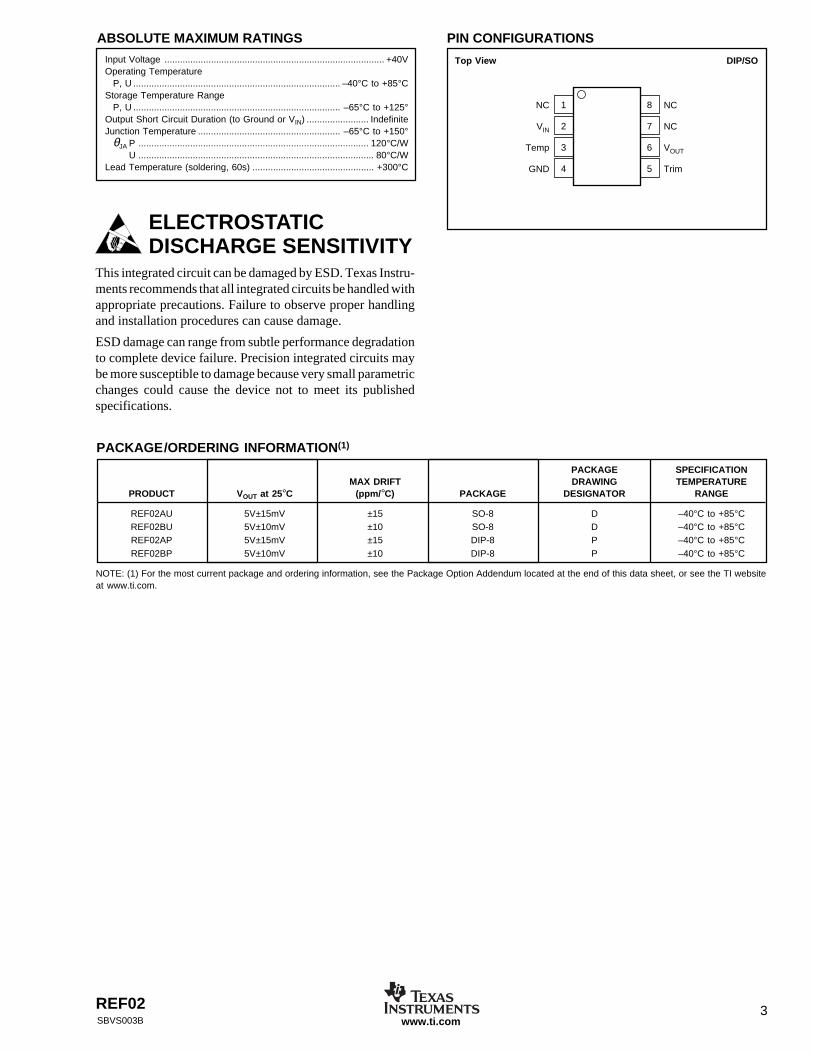
Input Voltage ..................................................................................... +40VOperating Temperature
P, U ................................................................................ –40°C to +85°CStorage Temperature Range
P, U ................................................................................ –65°C to +125°Output Short Circuit Duration (to Ground or VIN) ........................ IndefiniteJunction Temperature ....................................................... –65°C to +150°
θJA P ......................................................................................... 120°C/WU ........................................................................................... 80°C/W
Lead Temperature (soldering, 60s) ............................................... +300°C
ABSOLUTE MAXIMUM RATINGS PIN CONFIGURATIONS
Top View DIP/SO
NC
VIN
Temp
GND
NC
NC
VOUT
Trim
1
2
3
4
8
7
6
5
ELECTROSTATICDISCHARGE SENSITIVITY
This integrated circuit can be damaged by ESD. Texas Instru-ments recommends that all integrated circuits be handled withappropriate precautions. Failure to observe proper handlingand installation procedures can cause damage.
ESD damage can range from subtle performance degradationto complete device failure. Precision integrated circuits maybe more susceptible to damage because very small parametricchanges could cause the device not to meet its publishedspecifications.
PACKAGE/ORDERING INFORMATION(1)
PACKAGE SPECIFICATIONMAX DRIFT DRAWING TEMPERATURE
PRODUCT VOUT at 25°C (ppm/°C) PACKAGE DESIGNATOR RANGE
REF02AU 5V±15mV ±15 SO-8 D –40°C to +85°CREF02BU 5V±10mV ±10 SO-8 D –40°C to +85°CREF02AP 5V±15mV ±15 DIP-8 P –40°C to +85°CREF02BP 5V±10mV ±10 DIP-8 P –40°C to +85°C
NOTE: (1) For the most current package and ordering information, see the Package Option Addendum located at the end of this data sheet, or see the TI websiteat www.ti.com.
REF024SBVS003Bwww.ti.com
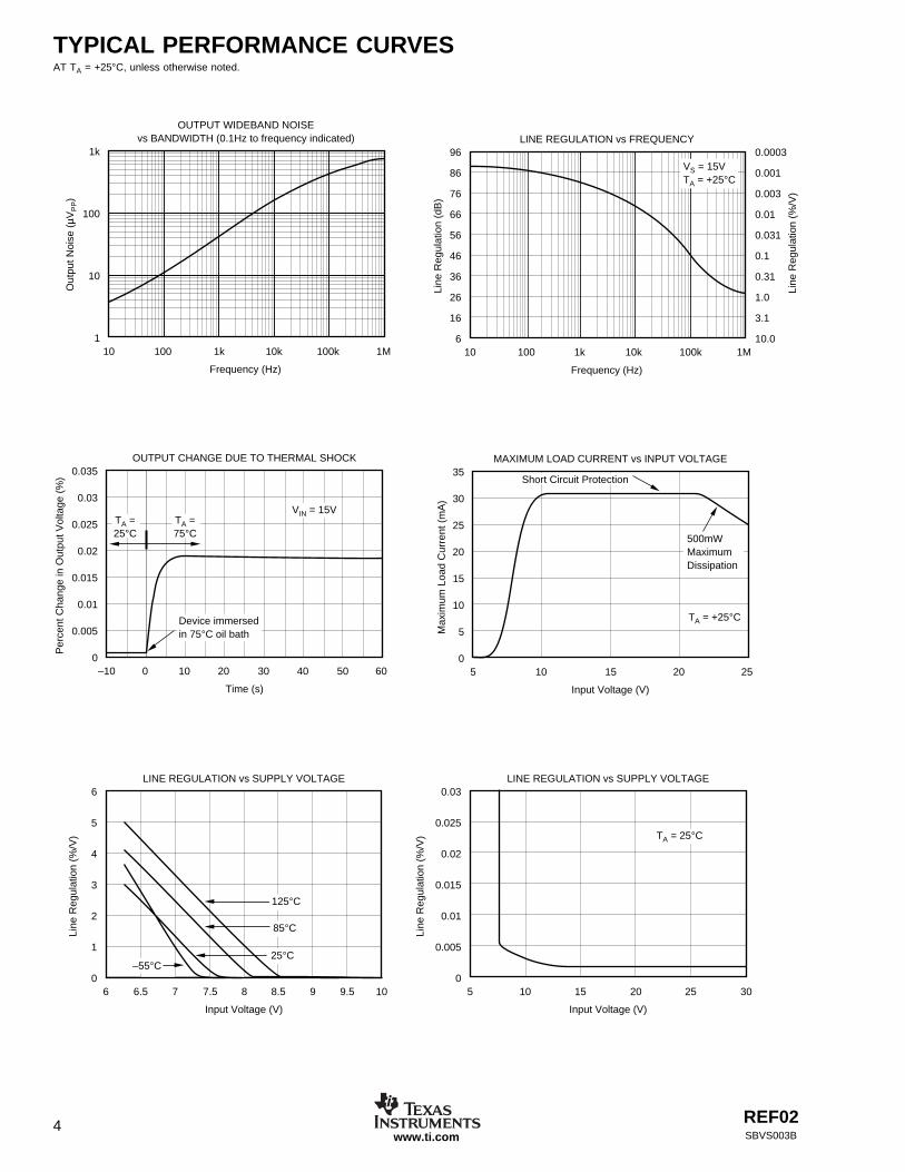
TYPICAL PERFORMANCE CURVESAT TA = +25°C, unless otherwise noted.
OUTPUT WIDEBAND NOISEvs BANDWIDTH (0.1Hz to frequency indicated)
Frequency (Hz)
Out
put N
oise
(µV
PP)
10 100 1k 10k 100k 1M
1k
100
10
1
OUTPUT CHANGE DUE TO THERMAL SHOCK
Time (s)
Per
cent
Cha
nge
in O
utpu
t Vol
tage
(%
)
0.035
0.03
0.025
0.02
0.015
0.01
0.005
0–10 0 10 20 30 40 50 60
Device immersedin 75°C oil bath
TA =25°C
TA =75°C
VIN = 15V
MAXIMUM LOAD CURRENT vs INPUT VOLTAGE
Max
imum
Loa
d C
urre
nt (
mA
)
Input Voltage (V)
5 10 15 20 25
35
30
25
20
15
10
5
0
500mWMaximumDissipation
Short Circuit Protection
TA = +25°C
LINE REGULATION vs SUPPLY VOLTAGE
Input Voltage (V)
6
5
4
3
2
1
0
Line
Reg
ulat
ion
(%/V
)
6 6.5 7 7.5 8 8.5 9 9.5 10
85°C
25°C
125°C
–55°C
LINE REGULATION vs SUPPLY VOLTAGE
Input Voltage (V)
0.03
0.025
0.02
0.015
0.01
0.005
0
Line
Reg
ulat
ion
(%/V
)
5
TA = 25°C
10 15 20 25 30
LINE REGULATION vs FREQUENCY
Line
Reg
ulat
ion
(dB
)
Frequency (Hz)
10 100 1k 10k 100k 1M
Line
Reg
ulat
ion
(%/V
)
96
86
76
66
56
46
36
26
16
6
0.0003
0.001
0.003
0.01
0.031
0.1
0.31
1.0
3.1
10.0
VS = 15VTA = +25°C
REF02 5SBVS003B www.ti.com
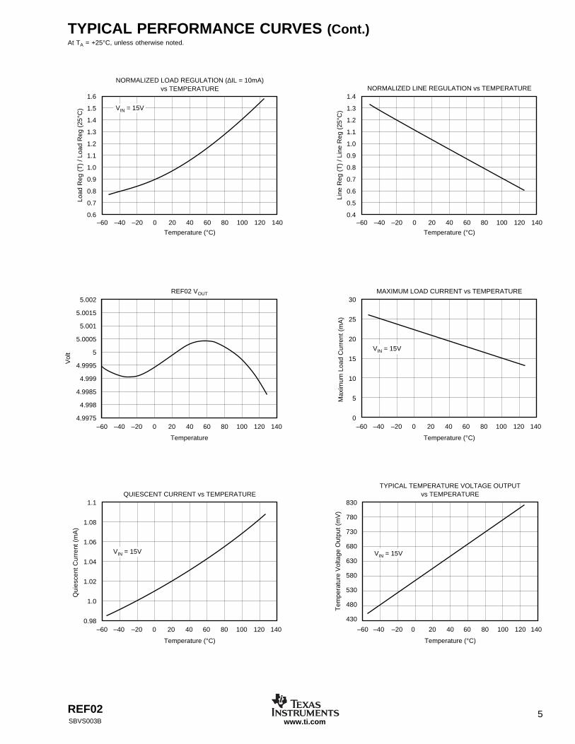
TYPICAL PERFORMANCE CURVES (Cont.)At TA = +25°C, unless otherwise noted.
NORMALIZED LOAD REGULATION (∆IL = 10mA)vs TEMPERATURE
–60
1.6
1.5
1.4
1.3
1.2
1.1
1.0
0.9
0.8
0.7
0.6
Temperature (°C)
–40 –20 0 20 40 60 80 100 120 140
Load
Reg
(T
) / L
oad
Reg
(25
°C) VIN = 15V
NORMALIZED LINE REGULATION vs TEMPERATURE
–60
1.4
1.3
1.2
1.1
1.0
0.9
0.8
0.7
0.6
0.5
0.4
Temperature (°C)
–40 –20 0 20 40 60 80 100 120 140
Line
Reg
(T
) / L
ine
Reg
(25
°C)
REF02 VOUT
Temperature
Vol
t
5.002
5.0015
5.001
5.0005
5
4.9995
4.999
4.9985
4.998
4.9975–60 –40 –20 0 20 40 60 80 100 120 140
MAXIMUM LOAD CURRENT vs TEMPERATURE
Temperature (°C)
30
25
20
15
10
5
0
Max
imum
Loa
d C
urre
nt (
mA
)
–60 –40 –20 0 20 40 60 80 100 120 140
VIN = 15V
QUIESCENT CURRENT vs TEMPERATURE
Temperature (°C)
1.1
1.08
1.06
1.04
1.02
1.0
0.98
Qui
esce
nt C
urre
nt (
mA
)
–60 –40 –20 0 20 40 60 80 100 120 140
VIN = 15V
TYPICAL TEMPERATURE VOLTAGE OUTPUTvs TEMPERATURE
Tem
pera
ture
Vol
tage
Out
put (
mV
)
Temperature (°C)
–60 –40 –20 0 20 40 60 80 100 120 140
830
780
730
680
630
580
530
480
430
VIN = 15V
REF026SBVS003Bwww.ti.com
TYPICAL PERFORMANCE CURVES (Cont.)At TA = +25°C, unless otherwise noted.
LONG-TERM STABILITY (1st 1000h)
Hours
0 24 48 72 96 168
192
240
336
408
504
576
696
744
864
912
1008
ppm
200
150
100
50
0
–50
–100
–150
–200
–250
LONG-TERM STABILITY (2nd 1000h)
Hours
1008
1080
1176
1272
1344
1440
1536
1608
1680
1776
1848
1944
ppm
200
150
100
50
0
–50
–100
–150
–200
–250
0 19441008504
LONG TERM STABILITY (2000h)
Hours
ppm
300
200
100
0
–100
–200
–300
REF02 7SBVS003B www.ti.com
OUTPUT ADJUSTMENT
The REF02 trim terminal can be used to adjust the voltageover a 5V ±150mV range. This feature allows the systemdesigner to trim system errors by setting the reference to avoltage other than 5V, including 5.12V(1) for binary applica-tions (see circuit on page 1).
Adjustment of the output does not significantly affect thetemperature performance of the device. The temperaturecoefficient change is approximately 0.7ppm/°C for 100mV ofoutput adjustment.
NOTE: (1) 20mV LSB for 8-bit applications.
TYPICAL APPLICATIONS
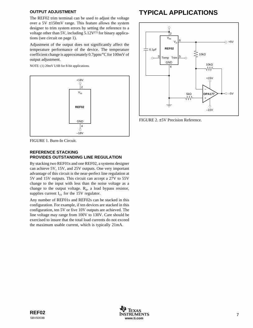
5kΩ OPA177
10kΩ
10kΩ
–15V
+15V
–5V
+5V
Trim
GND
VIN
3 5
4
2
REF020.1µF
VO
Temp
6
FIGURE 2. ±5V Precision Reference.
REF02
GND
2
4
–18V
+18V
VIN
FIGURE 1. Burn-In Circuit.
REFERENCE STACKINGPROVIDES OUTSTANDING LINE REGULATION
By stacking two REF01s and one REF02, a systems designercan achieve 5V, 15V, and 25V outputs. One very importantadvantage of this circuit is the near-perfect line regulation at5V and 15V outputs. This circuit can accept a 27V to 55Vchange to the input with less than the noise voltage as achange to the output voltage. RB, a load bypass resistor,supplies current ISY for the 15V regulator.
Any number of REF01s and REF02s can be stacked in thisconfiguration. For example, if ten devices are stacked in thisconfiguration, ten 5V or five 10V outputs are achieved. Theline voltage may range from 100V to 130V. Care should beexercised to insure that the total load currents do not exceedthe maximum usable current, which is typically 21mA.
PACKAGE OPTION ADDENDUM
www.ti.com 8-Nov-2014
Addendum-Page 1
PACKAGING INFORMATION
Orderable Device Status(1)
Package Type PackageDrawing
Pins PackageQty
Eco Plan(2)
Lead/Ball Finish(6)
MSL Peak Temp(3)
Op Temp (°C) Device Marking(4/5)
Samples
REF02AP ACTIVE PDIP P 8 50 Green (RoHS& no Sb/Br)
CU NIPDAU N / A for Pkg Type REF02AP
REF02APG4 ACTIVE PDIP P 8 50 Green (RoHS& no Sb/Br)
CU NIPDAU N / A for Pkg Type REF02AP
REF02AU ACTIVE SOIC D 8 75 Green (RoHS& no Sb/Br)
CU NIPDAU Level-3-260C-168 HR -40 to 85 REF02AU
REF02AU/2K5 ACTIVE SOIC D 8 2500 Green (RoHS& no Sb/Br)
CU NIPDAU Level-3-260C-168 HR -40 to 85 REF02AU
REF02AU/2K5E4 ACTIVE SOIC D 8 2500 Green (RoHS& no Sb/Br)
CU NIPDAU Level-3-260C-168 HR -40 to 85 REF02AU
REF02AUE4 ACTIVE SOIC D 8 75 Green (RoHS& no Sb/Br)
CU NIPDAU Level-3-260C-168 HR -40 to 85 REF02AU
REF02AUG4 ACTIVE SOIC D 8 75 Green (RoHS& no Sb/Br)
CU NIPDAU Level-3-260C-168 HR -40 to 85 REF02AU
REF02BP ACTIVE PDIP P 8 50 Green (RoHS& no Sb/Br)
CU NIPDAU N / A for Pkg Type REF02BP
REF02BPG4 ACTIVE PDIP P 8 50 Green (RoHS& no Sb/Br)
CU NIPDAU N / A for Pkg Type REF02BP
REF02BU ACTIVE SOIC D 8 75 Green (RoHS& no Sb/Br)
CU NIPDAU Level-3-260C-168 HR -40 to 85 REF02BU
REF02BU/2K5 ACTIVE SOIC D 8 2500 Green (RoHS& no Sb/Br)
CU NIPDAU Level-3-260C-168 HR -40 to 85 REF02BU
REF02BU/2K5E4 ACTIVE SOIC D 8 2500 Green (RoHS& no Sb/Br)
CU NIPDAU Level-3-260C-168 HR -40 to 85 REF02BU
REF02BUE4 ACTIVE SOIC D 8 75 Green (RoHS& no Sb/Br)
CU NIPDAU Level-3-260C-168 HR -40 to 85 REF02BU
REF02BUG4 ACTIVE SOIC D 8 75 Green (RoHS& no Sb/Br)
CU NIPDAU Level-3-260C-168 HR -40 to 85 REF02BU
(1) The marketing status values are defined as follows:ACTIVE: Product device recommended for new designs.LIFEBUY: TI has announced that the device will be discontinued, and a lifetime-buy period is in effect.NRND: Not recommended for new designs. Device is in production to support existing customers, but TI does not recommend using this part in a new design.PREVIEW: Device has been announced but is not in production. Samples may or may not be available.OBSOLETE: TI has discontinued the production of the device.
PACKAGE OPTION ADDENDUM
www.ti.com 8-Nov-2014
Addendum-Page 2
(2) Eco Plan - The planned eco-friendly classification: Pb-Free (RoHS), Pb-Free (RoHS Exempt), or Green (RoHS & no Sb/Br) - please check http://www.ti.com/productcontent for the latest availabilityinformation and additional product content details.TBD: The Pb-Free/Green conversion plan has not been defined.Pb-Free (RoHS): TI's terms "Lead-Free" or "Pb-Free" mean semiconductor products that are compatible with the current RoHS requirements for all 6 substances, including the requirement thatlead not exceed 0.1% by weight in homogeneous materials. Where designed to be soldered at high temperatures, TI Pb-Free products are suitable for use in specified lead-free processes.Pb-Free (RoHS Exempt): This component has a RoHS exemption for either 1) lead-based flip-chip solder bumps used between the die and package, or 2) lead-based die adhesive used betweenthe die and leadframe. The component is otherwise considered Pb-Free (RoHS compatible) as defined above.Green (RoHS & no Sb/Br): TI defines "Green" to mean Pb-Free (RoHS compatible), and free of Bromine (Br) and Antimony (Sb) based flame retardants (Br or Sb do not exceed 0.1% by weightin homogeneous material)
(3) MSL, Peak Temp. - The Moisture Sensitivity Level rating according to the JEDEC industry standard classifications, and peak solder temperature.
(4) There may be additional marking, which relates to the logo, the lot trace code information, or the environmental category on the device.
(5) Multiple Device Markings will be inside parentheses. Only one Device Marking contained in parentheses and separated by a "~" will appear on a device. If a line is indented then it is a continuationof the previous line and the two combined represent the entire Device Marking for that device.
(6) Lead/Ball Finish - Orderable Devices may have multiple material finish options. Finish options are separated by a vertical ruled line. Lead/Ball Finish values may wrap to two lines if the finishvalue exceeds the maximum column width.
Important Information and Disclaimer:The information provided on this page represents TI's knowledge and belief as of the date that it is provided. TI bases its knowledge and belief on informationprovided by third parties, and makes no representation or warranty as to the accuracy of such information. Efforts are underway to better integrate information from third parties. TI has taken andcontinues to take reasonable steps to provide representative and accurate information but may not have conducted destructive testing or chemical analysis on incoming materials and chemicals.TI and TI suppliers consider certain information to be proprietary, and thus CAS numbers and other limited information may not be available for release.
In no event shall TI's liability arising out of such information exceed the total purchase price of the TI part(s) at issue in this document sold by TI to Customer on an annual basis.
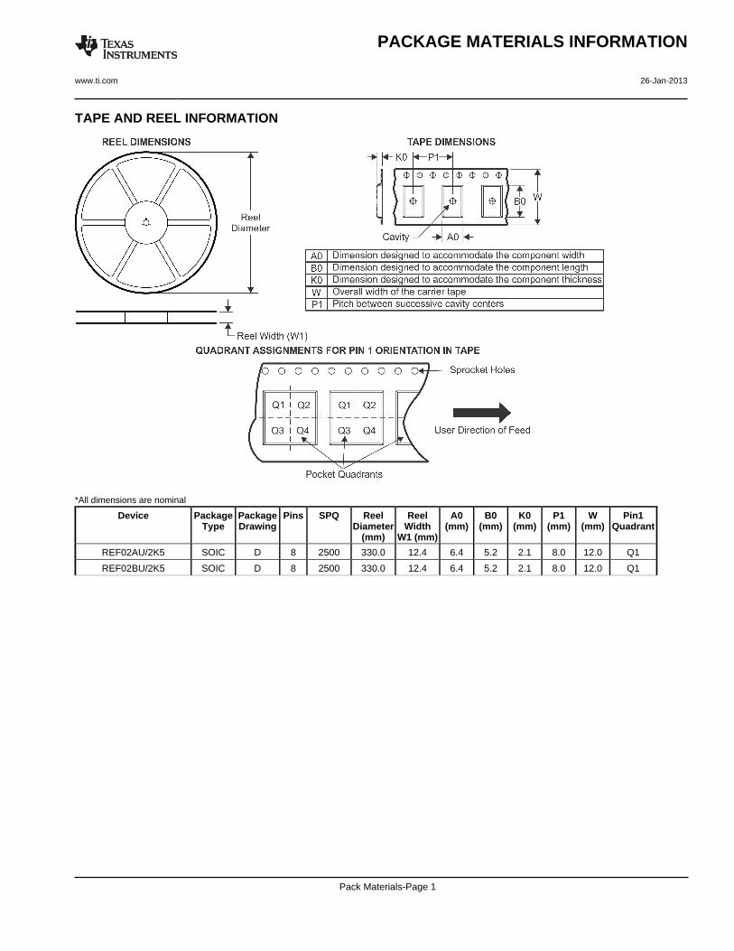
TAPE AND REEL INFORMATION
*All dimensions are nominal
Device PackageType
PackageDrawing
Pins SPQ ReelDiameter
(mm)
ReelWidth
W1 (mm)
A0(mm)
B0(mm)
K0(mm)
P1(mm)
W(mm)
Pin1Quadrant
REF02AU/2K5 SOIC D 8 2500 330.0 12.4 6.4 5.2 2.1 8.0 12.0 Q1
REF02BU/2K5 SOIC D 8 2500 330.0 12.4 6.4 5.2 2.1 8.0 12.0 Q1
PACKAGE MATERIALS INFORMATION
www.ti.com 26-Jan-2013
Pack Materials-Page 1
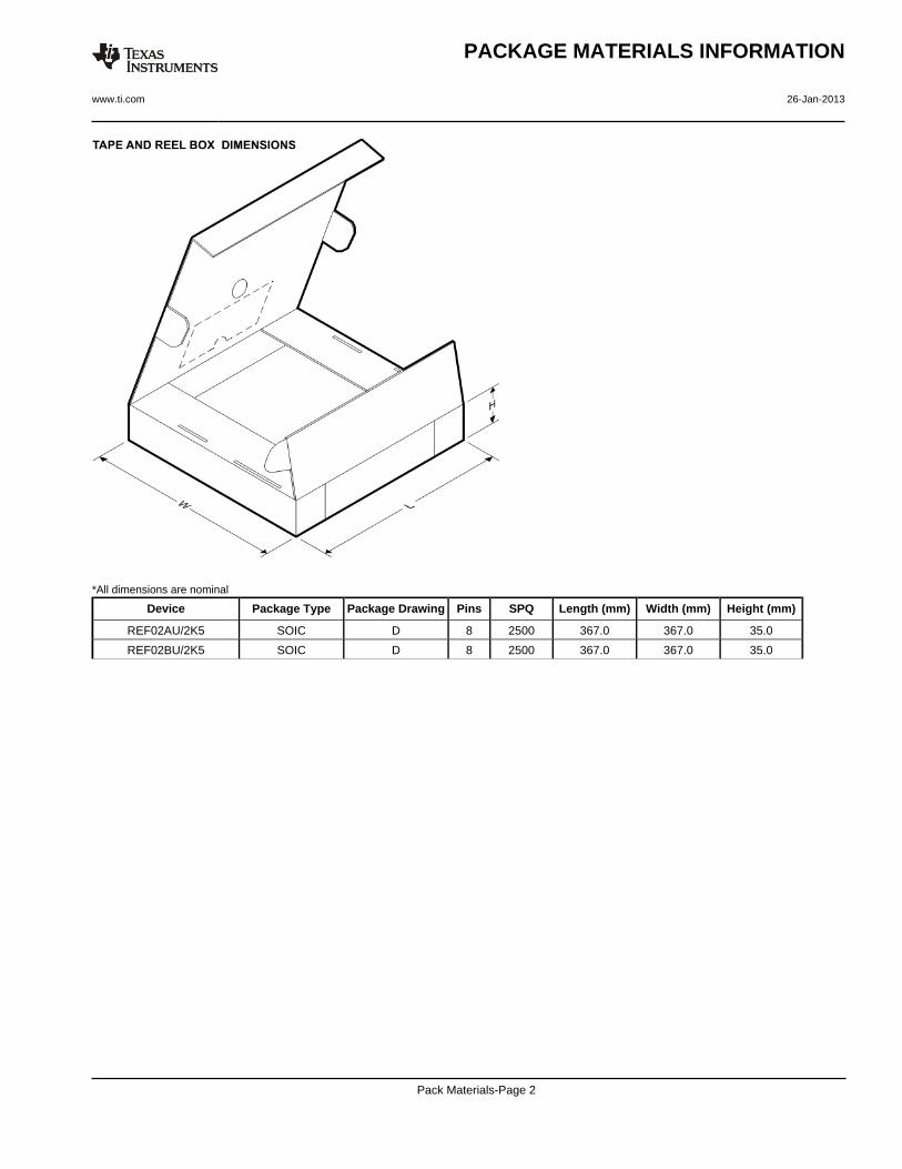
*All dimensions are nominal
Device Package Type Package Drawing Pins SPQ Length (mm) Width (mm) Height (mm)
REF02AU/2K5 SOIC D 8 2500 367.0 367.0 35.0
REF02BU/2K5 SOIC D 8 2500 367.0 367.0 35.0
PACKAGE MATERIALS INFORMATION
www.ti.com 26-Jan-2013
Pack Materials-Page 2
IMPORTANT NOTICETexas Instruments Incorporated and its subsidiaries (TI) reserve the right to make corrections, enhancements, improvements and otherchanges to its semiconductor products and services per JESD46, latest issue, and to discontinue any product or service per JESD48, latestissue. Buyers should obtain the latest relevant information before placing orders and should verify that such information is current andcomplete. All semiconductor products (also referred to herein as “components”) are sold subject to TI’s terms and conditions of salesupplied at the time of order acknowledgment.TI warrants performance of its components to the specifications applicable at the time of sale, in accordance with the warranty in TI’s termsand conditions of sale of semiconductor products. Testing and other quality control techniques are used to the extent TI deems necessaryto support this warranty. Except where mandated by applicable law, testing of all parameters of each component is not necessarilyperformed.TI assumes no liability for applications assistance or the design of Buyers’ products. Buyers are responsible for their products andapplications using TI components. To minimize the risks associated with Buyers’ products and applications, Buyers should provideadequate design and operating safeguards.TI does not warrant or represent that any license, either express or implied, is granted under any patent right, copyright, mask work right, orother intellectual property right relating to any combination, machine, or process in which TI components or services are used. Informationpublished by TI regarding third-party products or services does not constitute a license to use such products or services or a warranty orendorsement thereof. Use of such information may require a license from a third party under the patents or other intellectual property of thethird party, or a license from TI under the patents or other intellectual property of TI.Reproduction of significant portions of TI information in TI data books or data sheets is permissible only if reproduction is without alterationand is accompanied by all associated warranties, conditions, limitations, and notices. TI is not responsible or liable for such altereddocumentation. Information of third parties may be subject to additional restrictions.Resale of TI components or services with statements different from or beyond the parameters stated by TI for that component or servicevoids all express and any implied warranties for the associated TI component or service and is an unfair and deceptive business practice.TI is not responsible or liable for any such statements.Buyer acknowledges and agrees that it is solely responsible for compliance with all legal, regulatory and safety-related requirementsconcerning its products, and any use of TI components in its applications, notwithstanding any applications-related information or supportthat may be provided by TI. Buyer represents and agrees that it has all the necessary expertise to create and implement safeguards whichanticipate dangerous consequences of failures, monitor failures and their consequences, lessen the likelihood of failures that might causeharm and take appropriate remedial actions. Buyer will fully indemnify TI and its representatives against any damages arising out of the useof any TI components in safety-critical applications.In some cases, TI components may be promoted specifically to facilitate safety-related applications. With such components, TI’s goal is tohelp enable customers to design and create their own end-product solutions that meet applicable functional safety standards andrequirements. Nonetheless, such components are subject to these terms.No TI components are authorized for use in FDA Class III (or similar life-critical medical equipment) unless authorized officers of the partieshave executed a special agreement specifically governing such use.Only those TI components which TI has specifically designated as military grade or “enhanced plastic” are designed and intended for use inmilitary/aerospace applications or environments. Buyer acknowledges and agrees that any military or aerospace use of TI componentswhich have not been so designated is solely at the Buyer's risk, and that Buyer is solely responsible for compliance with all legal andregulatory requirements in connection with such use.TI has specifically designated certain components as meeting ISO/TS16949 requirements, mainly for automotive use. In any case of use ofnon-designated products, TI will not be responsible for any failure to meet ISO/TS16949.Products ApplicationsAudio www.ti.com/audio Automotive and Transportation www.ti.com/automotiveAmplifiers amplifier.ti.com Communications and Telecom www.ti.com/communicationsData Converters dataconverter.ti.com Computers and Peripherals www.ti.com/computersDLP® Products www.dlp.com Consumer Electronics www.ti.com/consumer-appsDSP dsp.ti.com Energy and Lighting www.ti.com/energyClocks and Timers www.ti.com/clocks Industrial www.ti.com/industrialInterface interface.ti.com Medical www.ti.com/medicalLogic logic.ti.com Security www.ti.com/securityPower Mgmt power.ti.com Space, Avionics and Defense www.ti.com/space-avionics-defenseMicrocontrollers microcontroller.ti.com Video and Imaging www.ti.com/videoRFID www.ti-rfid.comOMAP Applications Processors www.ti.com/omap TI E2E Community e2e.ti.comWireless Connectivity www.ti.com/wirelessconnectivity
Mailing Address: Texas Instruments, Post Office Box 655303, Dallas, Texas 75265Copyright © 2014, Texas Instruments Incorporated