Embed Size (px)
Citation preview
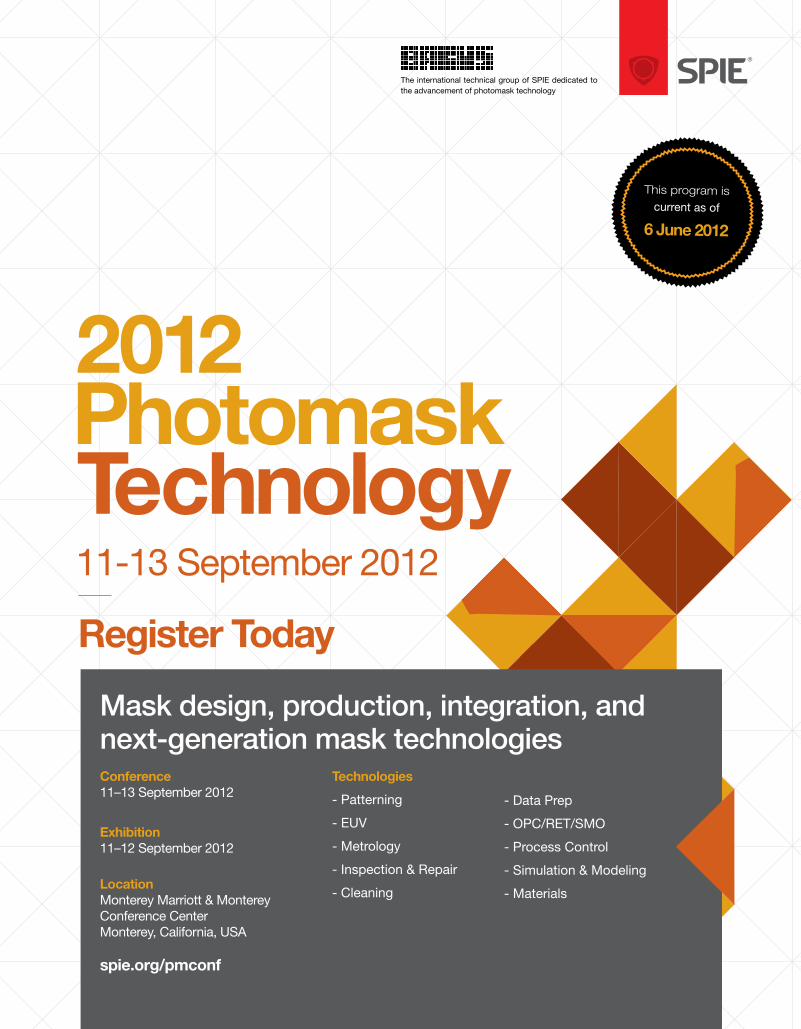
Mask design, production, integration, and next-generation mask technologies
Location Monterey Marriott & Monterey Conference CenterMonterey, California, USA
spie.org/pmconf
Conference 11–13 September 2012
Exhibition 11–12 September 2012
Technologies
- Patterning
- EUV
- Metrology
- Inspection & Repair
- Cleaning
The international technical group of SPIE dedicated to the advancement of photomask technology
2012
11-13 September 2012
Register Today
This program iscurrent as of
6 June 2012
- Data Prep
- OPC/RET/SMO
- Process Control
- Simulation & Modeling
- Materials
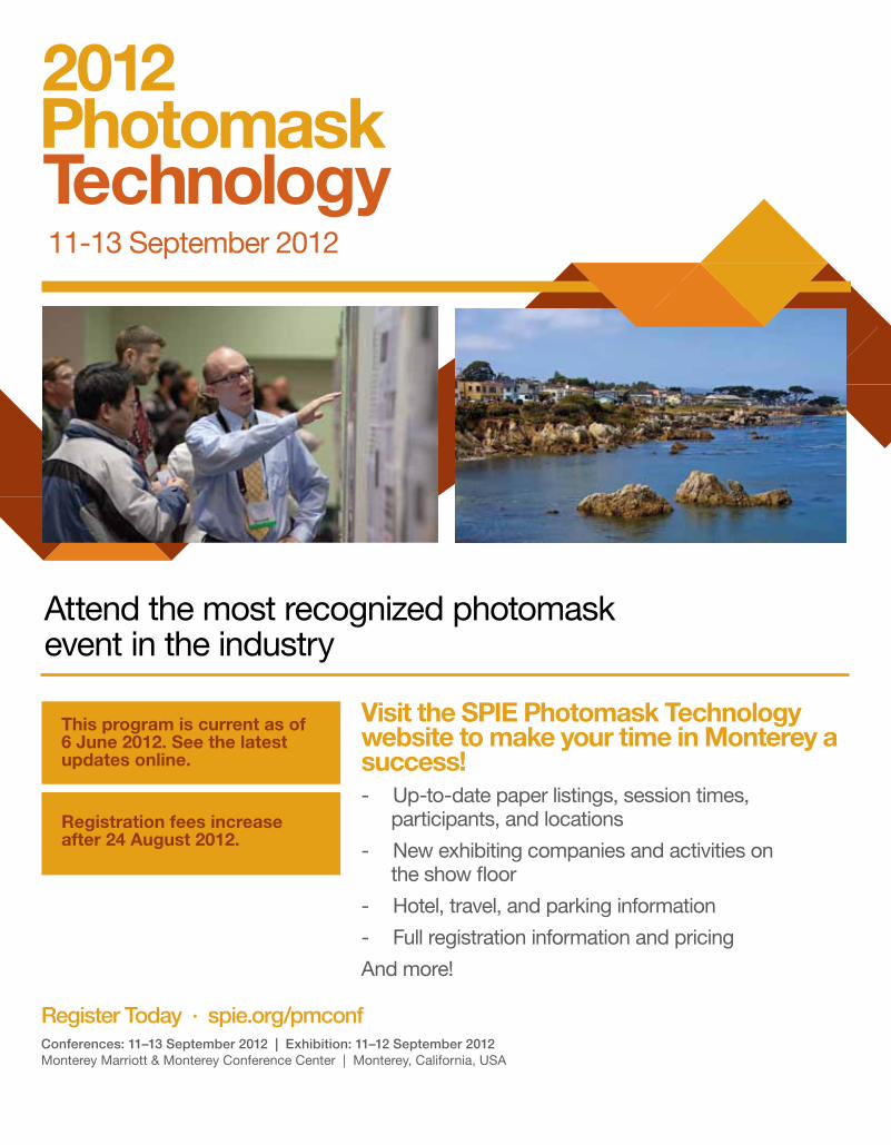
Attend the most recognized photomask event in the industry
This program is current as of 6 June 2012. See the latest updates online.
Registration fees increase after 24 August 2012.
Conferences: 11–13 September 2012 | Exhibition: 11–12 September 2012 Monterey Marriott & Monterey Conference Center | Monterey, California, USA
Register Today · spie.org/pmconf
Visit the SPIE Photomask Technology website to make your time in Monterey a success!- Up-to-date paper listings, session times,
participants, and locations
- New exhibiting companies and activities on the show floor
- Hotel, travel, and parking information
- Full registration information and pricing
And more!
2012
11-13 September 2012
SPIE Photomask Technology 2012 · spie.org/pmconf1
This program is current as of 6 June 2012. For latest updates: spie.org/pmconf
2012
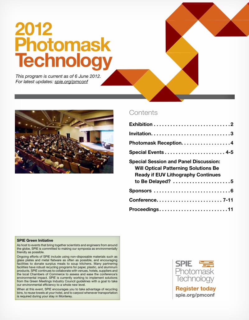
Contents
Exhibition. . . . . . . . . . . . . . . . . . . . . . . . . . . . . 2
Invitation. . . . . . . . . . . . . . . . . . . . . . . . . . . . . . 3
Photomask.Reception .. .. .. .. .. .. .. .. .. .. .. .. .. .. .. .. .. . 4
Special.Events. . . . . . . . . . . . . . . . . . . . . . . 4-5
Special.Session.and.Panel.Discussion:Will.Optical.Patterning.Solutions.Be.Ready.if.EUV.Lithography.Continues..to.Be.Delayed? . . . . . . . . . . . . . . . . . . . . . . 5
Sponsors . . . . . . . . . . . . . . . . . . . . . . . . . . . . . 6
Conference. . . . . . . . . . . . . . . . . . . . . . . . . 7-11
Proceedings. . . . . . . . . . . . . . . . . . . . . . . . . . 11.
Register.todayspie .org/pmconf
SPIE.Green.InitiativeAs host to events that bring together scientists and engineers from around the globe, SPIE is committed to making our symposia as environmentally friendly as possible.Ongoing efforts of SPIE include using non-disposable materials such as glass plates and metal flatware as often as possible, and encouraging facilities to donate surplus meals to soup kitchens. Many partnering facilities have robust recycling programs for paper, plastic, and aluminum products. SPIE continues to collaborate with venues, hotels, suppliers and the local Chambers of Commerce to assess and ease the conference’s environmental impact. SPIE is currently working to implement solutions from the Green Meetings Industry Council guidelines with a goal to take our environmental efficiency to a whole new level.When at this event, SPIE encourages you to take advantage of recycling bins, to reuse towels at your hotel, and to carpool whenever transportation is required during your stay in Monterey.
SPIE Photomask Technology 2012 · spie.org/pmconf2
Register.today:spie .org/pmconf
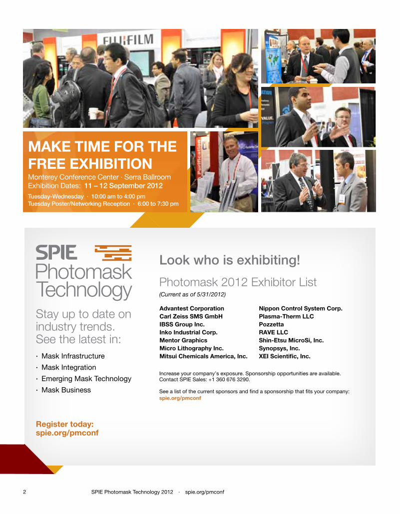
Look who is exhibiting!
Photomask 2012 Exhibitor List (Current as of 5/31/2012)
Stay up to date on industry trends. See the latest in: · Mask Infrastructure
· Mask Integration
· Emerging Mask Technology
· Mask Business
Advantest.CorporationCarl.Zeiss.SMS.GmbHIBSS.Group.Inc .Inko.Industrial.Corp .Mentor.GraphicsMicro.Lithography.Inc .Mitsui.Chemicals.America,.Inc .
Increase your company’s exposure. Sponsorship opportunities are available. Contact SPIE Sales: +1 360 676 3290.
See a list of the current sponsors and find a sponsorship that fits your company:spie .org/pmconf
MAkE.tIME.fOR.tHE..fREE.ExHIBItIOnMonterey Conference Center · Serra Ballroom Exhibition Dates: 11 – 12 September 2012Tuesday-Wednesday · 10:00 am to 4:00 pmTuesday Poster/Networking Reception · 6:00 to 7:30 pm
nippon.Control.System.Corp .Plasma-therm.LLCPozzettaRAVE.LLCShin-Etsu.MicroSi,.Inc .Synopsys,.Inc .xEI.Scientific,.Inc .
SPIE Photomask Technology 2012 · spie.org/pmconf3
Invitation from the Chairs
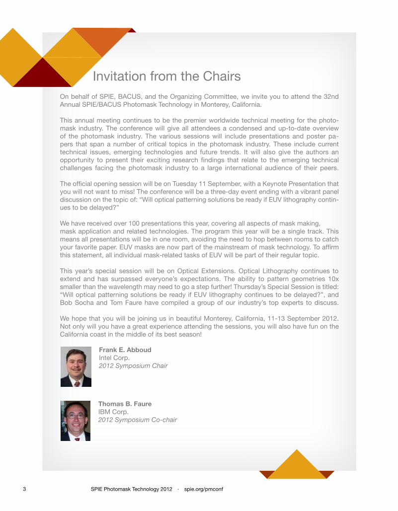
frank.E ..AbboudIntel Corp.2012 Symposium Chair
thomas.B ..faureIBM Corp.2012 Symposium Co-chair
On behalf of SPIE, BACUS, and the Organizing Committee, we invite you to attend the 32nd Annual SPIE/BACUS Photomask Technology in Monterey, California.
This annual meeting continues to be the premier worldwide technical meeting for the photo-mask industry. The conference will give all attendees a condensed and up-to-date overview of the photomask industry. The various sessions will include presentations and poster pa-pers that span a number of critical topics in the photomask industry. These include current technical issues, emerging technologies and future trends. It will also give the authors an opportunity to present their exciting research findings that relate to the emerging technical challenges facing the photomask industry to a large international audience of their peers.
The official opening session will be on Tuesday 11 September, with a Keynote Presentation that you will not want to miss! The conference will be a three-day event ending with a vibrant panel discussion on the topic of: “Will optical patterning solutions be ready if EUV lithography contin-ues to be delayed?”
We have received over 100 presentations this year, covering all aspects of mask making,mask application and related technologies. The program this year will be a single track. This means all presentations will be in one room, avoiding the need to hop between rooms to catch your favorite paper. EUV masks are now part of the mainstream of mask technology. To affirm this statement, all individual mask-related tasks of EUV will be part of their regular topic.
This year’s special session will be on Optical Extensions. Optical Lithography continues to extend and has surpassed everyone’s expectations. The ability to pattern geometries 10x smaller than the wavelength may need to go a step further! Thursday’s Special Session is titled: “Will optical patterning solutions be ready if EUV lithography continues to be delayed?”, and Bob Socha and Tom Faure have compiled a group of our industry’s top experts to discuss.
We hope that you will be joining us in beautiful Monterey, California, 11-13 September 2012. Not only will you have a great experience attending the sessions, you will also have fun on the California coast in the middle of its best season!
SPIE Photomask Technology 2012 · spie.org/pmconf4
Special Events
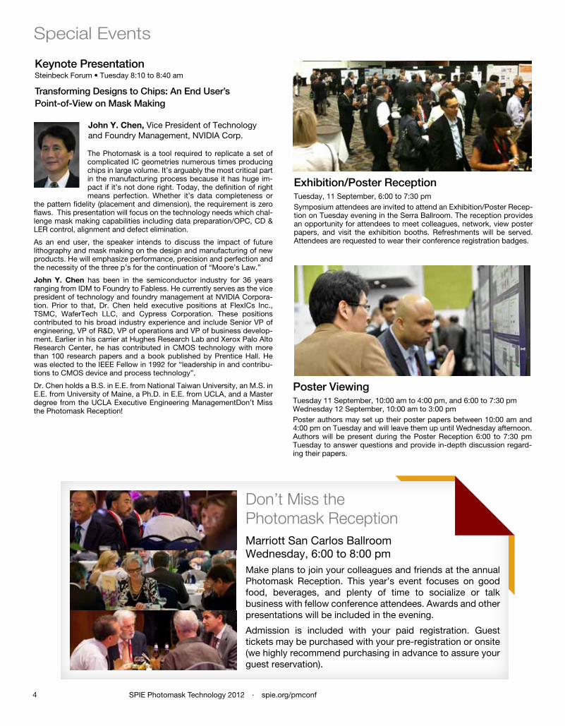
Exhibition/Poster Reception Tuesday, 11 September, 6:00 to 7:30 pm Symposium attendees are invited to attend an Exhibition/Poster Recep-tion on Tuesday evening in the Serra Ballroom. The reception provides an opportunity for attendees to meet colleagues, network, view poster papers, and visit the exhibition booths. Refreshments will be served. Attendees are requested to wear their conference registration badges.
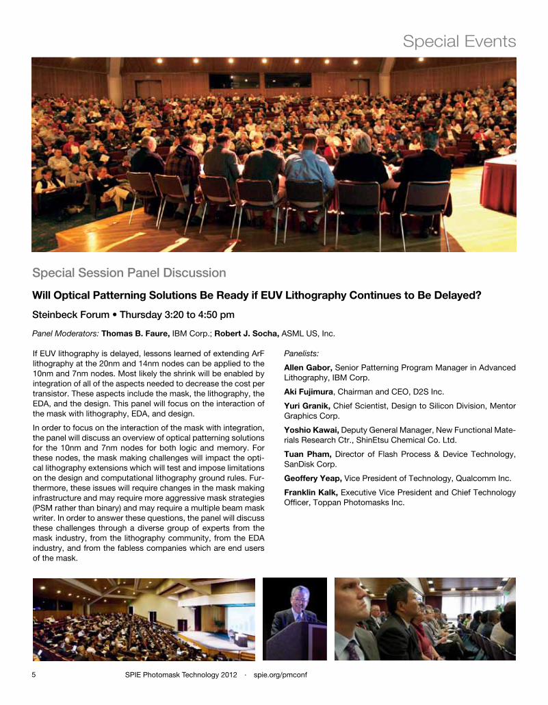
Poster ViewingTuesday 11 September, 10:00 am to 4:00 pm, and 6:00 to 7:30 pmWednesday 12 September, 10:00 am to 3:00 pmPoster authors may set up their poster papers between 10:00 am and 4:00 pm on Tuesday and will leave them up until Wednesday afternoon. Authors will be present during the Poster Reception 6:00 to 7:30 pm Tuesday to answer questions and provide in-depth discussion regard-ing their papers.
Don’t Miss the Photomask ReceptionMarriott San Carlos BallroomWednesday, 6:00 to 8:00 pmMake plans to join your colleagues and friends at the annual Photomask Reception. This year’s event focuses on good food, beverages, and plenty of time to socialize or talk business with fellow conference attendees. Awards and other presentations will be included in the evening.
Admission is included with your paid registration. Guest tickets may be purchased with your pre-registration or onsite (we highly recommend purchasing in advance to assure your guest reservation).
Keynote PresentationSteinbeck Forum • Tuesday 8:10 to 8:40 am
Transforming Designs to Chips: An End User’s Point-of-View on Mask Making
The Photomask is a tool required to replicate a set of complicated IC geometries numerous times producing chips in large volume. It’s arguably the most critical part in the manufacturing process because it has huge im-pact if it’s not done right. Today, the definition of right means perfection. Whether it’s data completeness or
the pattern fidelity (placement and dimension), the requirement is zero flaws. This presentation will focus on the technology needs which chal-lenge mask making capabilities including data preparation/OPC, CD & LER control, alignment and defect elimination.
As an end user, the speaker intends to discuss the impact of future lithography and mask making on the design and manufacturing of new products. He will emphasize performance, precision and perfection and the necessity of the three p’s for the continuation of “Moore’s Law.”
John. Y .. Chen has been in the semiconductor industry for 36 years ranging from IDM to Foundry to Fabless. He currently serves as the vice president of technology and foundry management at NVIDIA Corpora-tion. Prior to that, Dr. Chen held executive positions at FlexICs Inc., TSMC, WaferTech LLC, and Cypress Corporation. These positions contributed to his broad industry experience and include Senior VP of engineering, VP of R&D, VP of operations and VP of business develop-ment. Earlier in his carrier at Hughes Research Lab and Xerox Palo Alto Research Center, he has contributed in CMOS technology with more than 100 research papers and a book published by Prentice Hall. He was elected to the IEEE Fellow in 1992 for “leadership in and contribu-tions to CMOS device and process technology”.
Dr. Chen holds a B.S. in E.E. from National Taiwan University, an M.S. in E.E. from University of Maine, a Ph.D. in E.E. from UCLA, and a Master degree from the UCLA Executive Engineering ManagementDon’t Miss the Photomask Reception!
John.Y ..Chen, Vice President of Technology and Foundry Management, NVIDIA Corp.
SPIE Photomask Technology 2012 · spie.org/pmconf5
Special Events
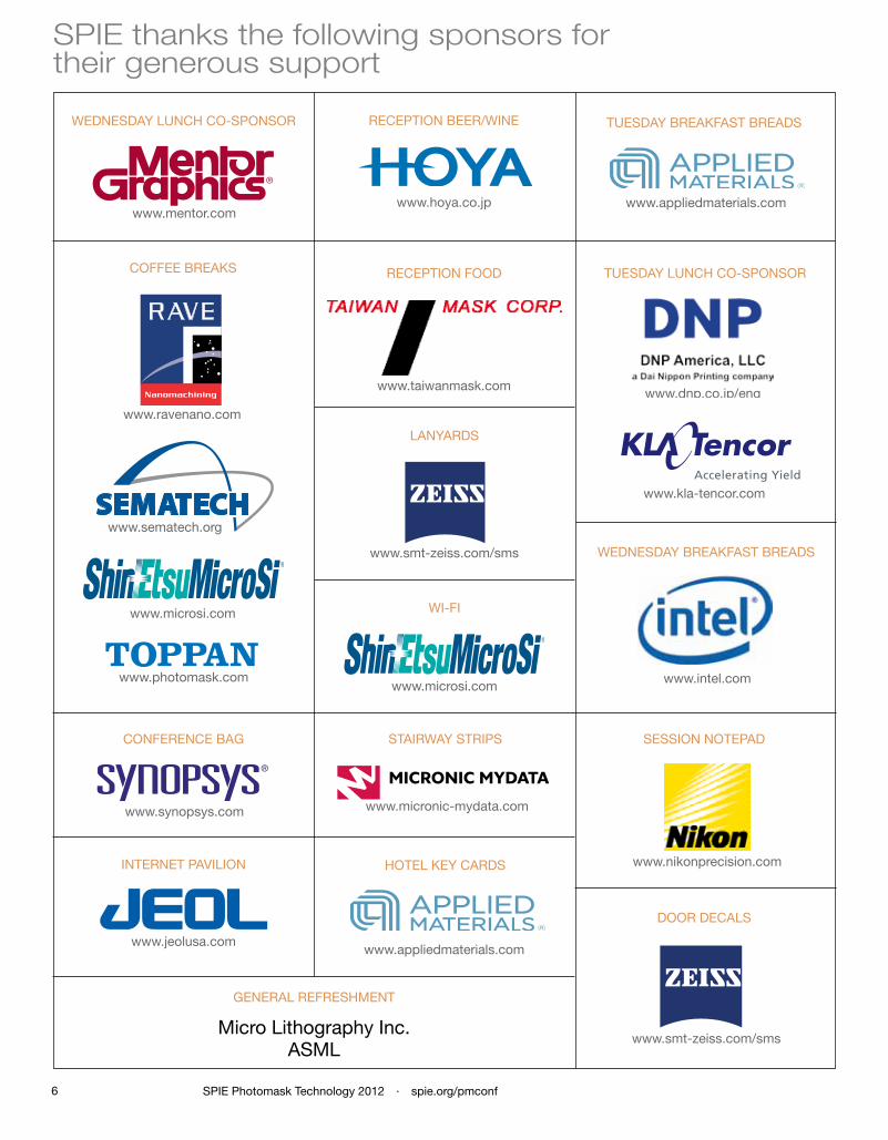
Special Session Panel Discussion
Will.Optical.Patterning.Solutions.Be.Ready.if.EUV.Lithography.Continues.to.Be.Delayed?
Steinbeck Forum • Thursday 3:20 to 4:50 pm
Panel Moderators: thomas.B ..faure, IBM Corp.; Robert.J ..Socha, ASML US, Inc.
If EUV lithography is delayed, lessons learned of extending ArF lithography at the 20nm and 14nm nodes can be applied to the 10nm and 7nm nodes. Most likely the shrink will be enabled by integration of all of the aspects needed to decrease the cost per transistor. These aspects include the mask, the lithography, the EDA, and the design. This panel will focus on the interaction of the mask with lithography, EDA, and design.
In order to focus on the interaction of the mask with integration, the panel will discuss an overview of optical patterning solutions for the 10nm and 7nm nodes for both logic and memory. For these nodes, the mask making challenges will impact the opti-cal lithography extensions which will test and impose limitations on the design and computational lithography ground rules. Fur-thermore, these issues will require changes in the mask making infrastructure and may require more aggressive mask strategies (PSM rather than binary) and may require a multiple beam mask writer. In order to answer these questions, the panel will discuss these challenges through a diverse group of experts from the mask industry, from the lithography community, from the EDA industry, and from the fabless companies which are end users of the mask.
Panelists:
Allen.Gabor, Senior Patterning Program Manager in Advanced Lithography, IBM Corp.
Aki.fujimura, Chairman and CEO, D2S Inc.
Yuri.Granik, Chief Scientist, Design to Silicon Division, Mentor Graphics Corp.
Yoshio.kawai, Deputy General Manager, New Functional Mate-rials Research Ctr., ShinEtsu Chemical Co. Ltd.
tuan.Pham, Director of Flash Process & Device Technology, SanDisk Corp.
Geoffery.Yeap, Vice President of Technology, Qualcomm Inc.
franklin.kalk, Executive Vice President and Chief Technology Officer, Toppan Photomasks Inc.
SPIE Photomask Technology 2012 · spie.org/pmconf6
GENERAL REFRESHMENT
Micro Lithography Inc.ASML
SPIE thanks the following sponsors for their generous support
TuESdAy BREAkFAST BREAdS
wEdNESdAy BREAkFAST BREAdS
wEdNESdAy LuNcH co-SpoNSoR
TuESdAy LuNcH co-SpoNSoR
www.dnp.co.jp/eng
INTERNET pAvILIoN
coNFERENcE BAG STAIRwAy STRIpS
dooR dEcALS
SESSIoN NoTEpAd
HoTEL kEy cARdS
coFFEE BREAkS
www.jeolusa.com
www.ravenano.com
www.smt-zeiss.com/sms
www.nikonprecision.com
www.smt-zeiss.com/sms
www.microsi.com
www.kla-tencor.com
www.intel.com
www.appliedmaterials.com
www.appliedmaterials.com
www.micronic-mydata.com
www.microsi.com
www.synopsys.com
www.photomask.com
www.sematech.org
LANyARdS
wI-FI
www.mentor.com
REcEpTIoN BEER/wINE
www.hoya.co.jp
REcEpTIoN Food
www.taiwanmask.com
SPIE Photomask Technology 2012 · spie.org/pmconf7
Conference 8522Tuesday-Thursday 11-13 September 2012 • Proceedings of SPIE Vol. 8522
Photomask.technologyConference Chair: frank.E ..Abboud,.Intel Corp. (United States)
Conference Co-Chair: thomas.B ..faure,.IBM Corp. (United States)
Program Committee: Ronald.R ..Bozak,.RAVE LLC (United States); William.H ..Broadbent,.KLA-Tencor Corp. (United States); Peter.D ..Buck,.Toppan Photomasks, Inc. (United States); Russell.B ..Cinque,.JEOL USA Inc. (United States); Glenn.R ..Dickey,.Shin-Etsu MicroSi, Inc. (United States); Uwe.Dietze,.Suss MicroTec AG (Germany); Aki.fujimura,.D2S, Inc. (United States); Emily.E ..Gallagher,.IBM Corp. (United States); Brian.J ..Grenon,.Grenon Consulting, Inc. (United States); naoya.Hayashi,.Dai Nippon Printing Co., Ltd. (Japan); Mark.t ..Jee,.HOyA Corp. USA (United States); Rik.Jonckheere,.IMEC (Belgium); Bryan.S ..kasprowicz,.Photronics, Inc. (United States); Byung-Gook.kim,.SAMSUNG Electronics Co., Ltd. (Korea, Republic of); Shy-Jay.Lin,.Taiwan Semiconductor Manufacturing Co. Ltd. (Taiwan); Wilhelm.Maurer,.Infineon Technologies AG (Germany); M ..Warren.Montgomery,.College of Nanoscale Science & Engineering (United States); thomas.H ..newman,.Micronic Laser Systems Inc. (United States); Hiroshi.nozue,.NuFlare Technology, Inc. (Japan); Linyong.Pang,.Luminescent Technologies, Inc. (United States); Emmanuel.Rausa,.Plasma-Therm LLC (United States); Douglas.J ..Resnick,.Molecular Imprints, Inc. (United States); thomas.Scherübl,.Carl Zeiss SMS GmbH (Germany); Steffen.Schulze,.Mentor Graphics Corp. (United States); Robert.J ..Socha,.ASML US, Inc. (United States); Anna.tchikoulaeva,.Lasertec U.S.A., Inc. Zweigniederlassung Deutschland (Germany); Jacek.k ..tyminski,.Nikon Research Corp. of America (United States); Banqiu.Wu,.Applied Materials, Inc. (United States); Stefan.Wurm,.SEMATECH North (United States)
tuesday.11.SeptemberOpening.Remarks.and.Introduction . . tues ..8:00.to.8:10.am
Session Chairs: frank.E ..Abboud,.Intel Corp. (United States); thomas.B ..faure,.IBM Corp. (United States)
keynote.Session. . . . . . . . . . . . . . . . . . tues ..8:10.to.8:50.am
transforming.designs.to.chips:.an.end.user’s.point-of-view.on.mask.making.(Keynote Presentation), John y. Chen, NVIDIA Corp. (United States) . . . . . . . . . . . . . . . . . . . . . . . . . . [8522-01]
SESSIOn.2. . . . . . . . . . . . . . . . . . . . . . . tues ..8:50.to.9:30.am
Invited.SessionSession Chairs: frank.E ..Abboud,.Intel Corp. (United States);
thomas.B ..faure,.IBM Corp. (United States)
2012.Mask.Industry.Assessment, Lloyd C. Litt, Matt Malloy, SEMATECH North (United States) . . . . . . . . . . . . . . . . . . . . . . . . . . . . . . . . . . . . . . . . . . . . [8522-02]
JPM12.Best.Paper (Presentation Only), , . . . . . . . . . . . . . . . . . . . . . . [8522-03]
SESSIOn.3. . . . . . . . . . . . . . . . . . . tues ..9:30.am.to.12:00.pm
PatterningSession Chairs: Jacek.k ..tyminski,.Nikon Precision Inc. (United
States); Robert.J ..Socha,.ASML US, Inc. (United States)
Improving.mask.CD.uniformity.using.MB-MDP.for.14nm.node.and.beyond, Byung-Gook Kim, Jin Choi, Jissong Park, Chan-Uk Jeon, SAMSUNG Electronics Co., Ltd. (Korea, Republic of); Ingo Bork, Ryan Pearman, Sterling Watson, Aki Fujimura, D2S, Inc. (United States) . . . . . . . . . . . . . . . . . . . . . . . . . . . . [8522-04]
Impact.of.an.etched.EUV.mask.black.border.on.imaging.and.overlay, Natalia V. Davydova, Robert C. de Kruif, Eelco van Setten, ASML Netherlands B.V. (Netherlands); Brid Connolly, Toppan Photomasks, Inc. (Germany); Norihito Fukugami, Toppan Printing Co., Ltd. (Japan); Ad Lammers, ASML Netherlands B.V. (Netherlands); John Zimmerman, Noreen Harned, ASML (United States) . . . . . . . . . . . . . . . . . . . . . . . . . . . . . . . . . . . . . . . . . . . . . . . . . . [8522-05]
An.enhanced.measure.of.mask.quality.using.separated.models, Anthony D. Adamov, Kazuyuki Hagiwara, Ingo Bork, D2S, Inc. (United States); Jin Choi, Jissong Park, Byung-Gook Kim, SAMSUNG Electronics Co., Ltd. (Korea, Republic of) . . . . . . . . . . . . . . . . . . . . . . . . . . . . . . . . . . . . . . . . . . . . . . [8522-06]
Cold-development.tool.and.technique.for.the.ultimate.resolution.of.ZEP520A.to.fabricate.an.EB.master.mold.for.nIL.for.1tbit/in2.BPM/HDD.development, Hideo Kobayashi, Hiromasa Iyama, Takeshi Kagatsume, Tsuyoshi Watanabe, HOyA Corp. (Japan) . . . . . . . . . . . . . . . . . . . . . . [8522-07]
Improvement.of.lithographic.performance.and.reduction.of.mask.cost.by.simple.OPC, Koichiro Tsujita, Canon Inc. (Japan); Michael C. Smayling, Tela Innovations, Inc. (United States); Valery Axelrad, Sequoia Design Systems, Inc. (United States); yuichi Gyoda, Ryo Nakayama, Canon Inc. (Japan) . . . [8522-08]
A.profile-aware.resist.model.with.an.image.location.dependant.threshold, Sylvain Moulis, Vincent Farys, STMicroelectronics (France); Jérôme Belledent, Romain Therese, CEA-LETI (France); Song Lan, Qian Zhao, Mu Feng, Laurent Depre, Russell J. Dover, Brion Technologies, Inc. (United States) . . . . [8522-09]
Lunch/Exhibition.Break. . . . . . . . . . . . . . . . . . . . . . . . . . . . . . 12:00 to 1:10 pm
SESSIOn.4. . . . . . . . . . . . . . . . . . . . . . . tues ..1:10.to.3:10.pm
MetrologySession Chairs: thomas.Scherübl,.Carl Zeiss SMS GmbH (Germany);
Peter.D ..Buck,.Toppan Photomasks, Inc. (United States)
CD.control.with.defect.inspection:.you.can.teach.an.old.dog.a.new.trick, Clemens S. Utzny, Albrecht Ullrich, Jan P. Heumann, Elias Mohn, Stefan Meusemann, Advanced Mask Technology Ctr. GmbH Co. KG (Germany) . . . . . . . . . . . . . . . . . . . . . . . . . . . . . . . . . . . . . . . . . . . . . . . [8522-10]
Study.of.critical.dimension.uniformity.(CDU).using.a.mask.inspector, Mei-Chun Lin, Ching-Fang yu, Mei-Tsu Lai, Luke T. H. Hsu, Angus Chin, Anthony yen, Taiwan Semiconductor Manufacturing Co. Ltd. (Taiwan) . . . . . . . [8522-11]
A.study.of.hot.spot.measurement.on.WLCD, Hidemichi Imai, Shingo yoshikawa, Dai Nippon Printing Co., Ltd. (Japan); Buttgereit Ute, Thomas Thaler, Carl Zeiss SMS Ltd. (Germany) . . . . . . . . . . . . . . . . . . . . . . . . . [8522-12]
An.impact.of.mask.CDU.and.local.CD.variation.on.intra-field.CDU, Junji Miyazaki, ASML Japan Co., Ltd. (Japan); Orion Mouraille, ASML Netherlands B.V. (Netherlands); Masaru Higuchi, yosuke Kojima, Shunsuke Sato, Toppan Printing Co., Ltd. (Japan); Jo Finders, ASML Netherlands B.V. (Netherlands); Hiroaki Morimoto, Toppan Printing Co., Ltd. (Japan) . . . . . . . . . . . . . . [8522-13]
Reticle.CDU.and.wafer.CDU.correlation.for.28nm.reticle.processes, GuoXiang Ning, Frank Richter, Thomas Thamm, GLOBALFOUNDRIES Dresden Module Two, GmbH & Co. KG (Germany); Paul W. Ackmann, GLOBALFOUNDRIES Inc. (United States); Marc Staples, Francois Weisbuch, Karin Kurth, Joerg Schenker, Andre Leschok, GLOBALFOUNDRIES Dresden Module Two, GmbH & Co. KG (Germany); Fang Hong Gn, GLOBALFOUNDRIES Singapore (Singapore) . . . . . . . . . . . . . . . . . . . . . . . . . . . . . . . . . . . . . . [8522-14]
Grid.calibration.and.matching.of.registration.tool.at.AMtC.to.previous.tool.generations.to.support.20nm.device.manufacturing.by.multiple.patterning.lithography, Klaus-Dieter Roeth, Michael Ferber, Frank Laske, KLA-Tencor MIE GmbH (Germany); Oliver Loeffler, Advanced Mask Technology Ctr. GmbH Co. KG (Germany) . . . . . . . . . . . . . . . . . . . . . . . . . . . . . . . . . . . . . . . . . . . . [8522-15]
SESSIOn.5. . . . . . . . . . . . . . . . . . . . . . . tues ..3:40.to.5:40.pm
Mask.Inspection.and.Repair.ISession Chairs: Emily.E ..Gallagher,.IBM Corp. (United States);
William.H ..Broadbent,.KLA-Tencor Corp. (United States)
Impact.of.EUVL.mask.surface.roughness.on.an.actinic.blank.inspection.image.and.a.wafer.image, Takeshi yamane, Tsuneo Terasawa, EUVL Infrastructure Development Ctr., Inc. (Japan) . . . . . . . . . . . . . . . . . . . . [8522-16]
Illuminating.EUVL.mask.defect.printability, Karen D. Badger, Zhengqing J. Qi, Emily E. Gallagher, IBM Corp. (United States); Kazunori Seki, Toppan Photomasks, Inc. (United States); Gregory R. McIntyre, IBM Corp. (United States) . . . . . . . . . . . . . . . . . . . . . . . . . . . . . . . . . . . . . . . . . . . . . . . . . . [8522-17]
SPIE Photomask Technology 2012 · spie.org/pmconf8
Conference 8522EUV.multilayer.defect.compensation.(MDC).by.absorber.pattern.modification:.calibrating.the.model.and.validate.accuracy.with.real.data, Linyong Pang, Masaki Satake, Vikram L. Tolani, Anthony D. Vacca, Peter Hu, Danping Peng, ying Li, Dongxue Chen, Luminescent Technologies (United States) . . . . . . . . . . . . . . . . . . . . . . . . . . . . . . . . . . . . . . . . . . . . . . . . . . [8522-18]
Capability.of.EBeyeM.for.EUV.mask.production, Masato Naka, Shinji yamaguchi, Motoki Kadowaki, Toru Koike, Takashi Hirano, Masamitsu Itoh, yuichiro yamazaki, Toshiba Corp. (Japan); Kenji Terao, Masahiro Hatakeyama, Kenji Watanabe, Hiroshi Sobukawa, Takeshi Murakami, Kiwamu Tsukamoto, Takehide Hayashi, Ryo Tajima, Norio Kimura, EBARA Corp. (Japan); Naoya Hayashi, Dai Nippon Printing Co., Ltd. (Japan) . . . . . . . . . . . . . . . . . . . [8522-19]
Electron-beam.inspection.of.16nm.HP.node.EUV.masks, Takeya Shimomura, DNP Corp. USA (United States); Shogo Narukawa, Tsukasa Abe, Tadahiko Takikawa, Naoya Hayashi, Dai Nippon Printing Co., Ltd. (Japan); Fei Wang, Long E. Ma, Chia-Wen Lin, yan Zhao, Chiyan Kuan, Jack y. Jau, Hermes-Microvision Inc., USA (United States) . . . . . . . . . . . . . . . . . . . . . . . . . . . . . . . . . . . . [8522-20]
EUV.mask.inspection.study.for.sub-20nm.device, Inkyun Shin, Gisung yoon, Won Sun Kim, Ji Hoon Na, Paul D. H. Chung, Chan-Uk Jeon, SAMSUNG Electronics Co., Ltd. (Korea, Republic of) . . . . . . . . . . . . . . . . . . . . . . . [8522-21]
Poster.Sessions. . . . . . . . . . . . . . . . . . . tues ..6:00.to.7:30.pmSession Chairs: Artur.P ..Balasinski,.Cypress Semiconductor Corp.
(United States); Mark.t ..Jee,.HOyA Corp. USA (United States); Abbas.Rastegar,.SEMATECH North (United States)
Exhibition/Poster ReceptionTuesday, 11 September, 6:00 to 7:30 pm
Symposium attendees are invited to attend an Exhibition/Poster Reception on Tuesday evening in the Serra Grand Ballroom. The reception provides an
opportunity for attendees to meet colleagues; network, view poster papers, and visit the exhibition booths. Refreshments will be served. Attendees are requested
to wear their conference registration badges.
Poster ViewingTuesday 20 September, 10 am to 4 pm, and 6 to 7:30 pm
Wednesday 21 September, 10 am to 3 pmPoster authors may set up their poster papers between 10 am and 4 pm on Tuesday and will leave them up until Wednesday afternoon. Authors will be
present during the Poster Reception 6:00 to 7:30 pm Tuesday to answer questions and provide in-depth discussion regarding their papers.
CleaningStudy.of.the.durability.of.the.Ru-capped.MoSi.multilayer.surface.under.megasonic.cleaning, Hüseyin Kurtuldu, Abbas Rastegar, Matthew House, SEMATECH North (United States) . . . . . . . . . . . . . . . . . . . . . . . . . . . . [8522-60]
Controlling.MegaSonic.performance.by.optimizing.cleaning.media’s.physical.and.gaseous.properties, SherJang Singh, SUSS MicroTec Inc. (United States) . . . . . . . . . . . . . . . . . . . . . . . . . . . . . . . . . . . . . . . . . . . . . . . . . . [8522-61]
Mask.Inspection.and.RepairLayout.relocation.considering.defect.inspection.tolerance.for.EUV.blank.defect.mitigation, yuelin Du, Hongbo Zhang, Martin D. F. Wong, Univ. of Illinois at Urbana-Champaign (United States) . . . . . . . . . . . . . . . . . . . . . . . . . [8522-62]
Efficient.simulation.of.EUV.multilayer.defects.with.rigorous.data.base.approach, Peter Evanschitzky, Andreas Erdmann, Fraunhofer-Institut für Integrierte System und Bauelementetechnologie (Germany) . . . . . . . . [8522-63]
High-brightness.EUV.light.source.for.actinic.mask.inspection.and.AIMS, Fariba Abreau, Samir S. Ellwi, Adlyte (Switzerland) . . . . . . . . . . . . . . . [8522-64]
fiducial.mark.requirements.from.the.viewpoints.of.actinic.blank.inspection.tool.for.phase-defect.mitigation.on.EUVL.mask, Tetsunori Murachi, Tsuyoshi Amano, Sung Hyun Oh, EUVL Infrastructure Development Ctr., Inc. (Japan) . . . . . . . . . . . . . . . . . . . . . . . . . . . . . . . . . . . . . . . . . . . . . . . . . . [8522-65]
EUVL.mask.inspection.at.Lyman.alpha, Thiago S. Jota, Thomas D. Milster, College of Optical Sciences, The Univ. of Arizona (United States) . . . . [8522-66]
EUV.mask-blank.defect.avoidance.solutions.assessment, Ahmad H. Elayat, Peter G. Thwaite, Steffen Schulze, Mentor Graphics Corp. (United States) . . . . . . . . . . . . . . . . . . . . . . . . . . . . . . . . . . . . . . . . . . . . . . . . . . [8522-67]
Backside. defect. printability. for. contact. layer. with. different. reticle. blank.material, GuoXiang Ning, Christian Holfeld, Daniel Fischer, GLOBALFOUNDRIES Dresden Module Two, GmbH & Co. KG (Germany); Paul W. Ackmann, GLOBALFOUNDRIES Inc. (United States); Andre Holfeld, GLOBALFOUNDRIES Dresden Module Two, GmbH & Co. KG (Germany); Martin Sczyrba, Advanced Mask Technology Ctr. GmbH Co. KG (Germany); Tino Hertzsch, Rolf Seltmann, GLOBALFOUNDRIES Dresden Module Two, GmbH & Co. KG (Germany); Angeline Ho, Fang Hong Gn, GLOBALFOUNDRIES Singapore (Singapore) . . . . [8522-68]
Automatic.defect.classification.using.hybrid.parallel.architecture.of.multi-core.CPU.and.GPU, Mark Pereira, Ravi R. Pai, Manabendra Maji, Rakesh K. Soni, R. Seshadri, SoftJin Technologies Pvt. Ltd. (India) . . . . . . . . . . . [8522-69]
key.issues.in.automatic.classification.of.defects.in.post-inspection.review.process.of.photomasks, Mark Pereira, Ravi R. Pai, Manabendra Maji, Samir Bhamidipati, Pradeep K. Patil, SoftJin Technologies Pvt. Ltd. (India) . [8522-70]
RDMS:.a.Windows-based.reticle.defect.search.database.with.AHDC.for.interconnected.mask.and.wafer.fabs, Saghir Munir, Reticle Labs. (United States) . . . . . . . . . . . . . . . . . . . . . . . . . . . . . . . . . . . . . . . . . . . . . . . . . . [8522-71]
Status.of.the.AIMS.tM.EUV.Project, Anthony D. Garetto, Jan Hendrik Peters, Sascha Perlitz, Ulrich Matejka, Carl Zeiss SMS GmbH (Germany); Dirk Hellweg, Markus R. Weiss, Carl Zeiss SMT GmbH (Germany) . . . . . . . . . . . . . . [8522-72]
Mask.Data.PreparationDouble.patterning.for.20nm.and.beyond:.design.rules.aware.splitting, Tamer S. Desouky, Mentor Graphics Egypt (Egypt); David A. Abercrombie, Mentor Graphics Corp. (United States); Omar H. El-Sewefy, Mentor Graphics Egypt (Egypt); Hojun Kim, Soo-Han Choi, SAMSUNG Electronics Co., Ltd. (Korea, Republic of) . . . . . . . . . . . . . . . . . . . . . . . . . . . . . . . . . . . . . . . . . . . . . . [8522-73]
Double-patterning.aware.placement.of.digital.ASIC.standard.cells, Heba Sharaf, Mentor Graphics Egypt (Egypt); Amr G. Wassal, Cairo Univ. (Egypt); Sherif Hammouda, Mentor Graphics Egypt (Egypt) . . . . . . . . . . . . . . . [8522-74]
Effective.user-defined.pattern.matching.method.for.reduction.of.yield.loss, Jaeyoung Choi, Sungho Jun, yeonah Shim, youngmi Kim, Jinho Park, Dongchan Lee, Dongbu HiTek Co., Ltd. (Korea, Republic of); Abhishek Vikram, Bo Su, Anchor Semiconductor, Inc. (United States) . . . . . . . . . . . . . . . . . . . . . [8522-75]
novel.customized.manufacturable.DfM.solutions, Mark Lu, Congshu Zhou, yi Tian, Soo Muay Goh, Shyue-Fong Quek, Hein-Mun Lam, Jian Zhang, GLOBALFOUNDRIES Singapore (Singapore) . . . . . . . . . . . . . . . . . . . . [8522-76]
Enhancement.of.mask.process.correction(MPC).through.dose.modulation.of.already.geometrically.corrected.layout.data, Murali M. Reddy, Bhardwaj D. S. S., Archana Rajagopalan, Nageswara Rao Guntupalli, Ravi R. Pai, SoftJin Technologies Pvt. Ltd. (India) . . . . . . . . . . . . . . . . . . . . . . . . . . . . . . . . [8522-77]
Efficient.Boolean.and.multi-input.flow.techniques.for.advanced.mask.data.processing, William Moore, Daniel Salazar, John Valadez, Synopsys, Inc. (United States) . . . . . . . . . . . . . . . . . . . . . . . . . . . . . . . . . . . . . . . . . . . . . . . . . . [8522-78]
Split-It!:.from.LELE.to.SADP.decomposition, yasmine A. Badr, Amr G. Wassal, Cairo Univ. (Egypt) . . . . . . . . . . . . . . . . . . . . . . . . . . . . . . . . . . [8522-79]
MetrologyDUV-based.metrology.extendibility.to.1x.node.mask.for.in-cell.registration.measurement, Hakseung Han, Hong-Seok Choi, HyeWook Jang, Paul D. H. Chung, Inkyun Shin, Chan-Uk Jeon, SAMSUNG Electronics Co., Ltd. (Korea, Republic of) . . . . . . . . . . . . . . . . . . . . . . . . . . . . . . . . . . . . . . . . . . . . . . [8522-80]
Photomask.quality.evaluation.using.lithography.simulation.and.precision.SEM.image.contour.data, Naoki Fukuda, Tsutomu Murakawa, Soichi Shida, Toshimichi Iwai, Jun Matsumoto, Takayuki Nakamura, Advantest Corp. (Japan); Kazuyuki Hagiwara, Shohei Matsushita, Daisuke Hara, D2S K.K. (Japan); Anthony D. Adamov, D2S, Inc. (United States) . . . . . . . . . . . . . . . . . . . . . . . . . . [8522-81]
Effective.method.for.PV-Band.comparison.to.lithography.and.etching.process, Ryoichi Matsuoka, Hitachi High-Technologies Corp. (Japan) [8522-82]
Grayscale.and.colorscale.microstructures.formed.by.layered.distributing.microdrops.over.polymer.film.for.photomask.utilized.in.single.mask.photolithography, Qingle Tang, Huazhong Research Institute of Electro-Optical Technology (China) . . . . . . . . . . . . . . . . . . . . . . . . . . . . . . . . . . . . . . . . [8522-83]
Correcting.image.placement.errors.using.registration.control.(RegC®).technology.in.the.photomask.periphery, Avi Cohen, Carl Zeiss SMS Ltd. (Israel); Falk Lange, Advanced Mask Technology Center GmbH & Co. KG (Germany); Guy Ben-Zvi, Erez Graitzer, Vladimir Dmitriev, Carl Zeiss SMS Ltd. (Israel) . . . . . . . . . . . . . . . . . . . . . . . . . . . . . . . . . . . . . . . . . . . . . . . . . . [8522-84]
Comparison.of.critical.dimension.uniformity.measurements.on.an.inspection.system.with.measurements.on.a.reticle.SEM, John M. Whittey, KLA-Tencor Corp. (United States); Jan P. Heumann, Albrecht Ullrich, Advanced Mask Technology Ctr. GmbH Co. KG (Germany); Edgardo Garcia, Mark Wagner, KLA-Tencor Corp. (United States); Norbert J. Schmidt, KLA-Tencor Germany (Germany); Clemens S. Utzny, Stefan Meusemann, Advanced Mask Technology Ctr. GmbH Co. KG (Germany) . . . . . . . . . . . . . . . . . . . . . . . . . . . . . . . . [8522-85]
Mask.Pattern.GeneratorsStudy.for.compensation.of.unexpected.image.placement.error.caused.by.variable.shape.beam.mask.writer.deflector, Hyunjoo Lee, SAMSUNG Electronics Co., Ltd. (Korea, Republic of) . . . . . . . . . . . . . . . . . . . . . . . [8522-86]
SPIE Photomask Technology 2012 · spie.org/pmconf9
Conference 8522Proximity.effect.correction.optimizing.image.quality.and.writing.time.for.an.electron.multi-beam.mask.writer, Martin Schulz, Synopsys GmbH (Germany); Jan Klikovits, IMS Nanofabrication AG (Austria); Thomas Klimpel, Synopsys GmbH (Germany); Alex Zepka, Synopsys, Inc. (United States); Hans-Jürgen Stock, Synopsys GmbH (Germany) . . . . . . . . . . . . . . . . . . . . . . . . . . . [8522-87]
Evaluation.of.CP.shape.correction.for.e-beam.writing, Masahiro Takizawa, Keita Bunya, Hideaki Isobe, Hideaki Komami, Kenji Abe, Masaki Kurokawa, Akio yamada, Kiichi Sakamoto, Takayuki Nakamura, Advantest Corp. (Japan); Kazusumi Kuwano, Masahiro Tateishi, D2S K.K. (Japan); Larry Chau, D2S, Inc. (United States) . . . . . . . . . . . . . . . . . . . . . . . . . . . . . . . . . . . . . . . . . . . . [8522-88]
An.8192-channel.grating.light.valve.modulator.for.direct-write.ultraviolet.lithography, Alexander P. Payne, Gregory Myatt, James A. Hunter, Michael yeung, Joshua Lu, Gregory Beach, Lars Eng, Silicon Light Machines (United States) . . . . . . . . . . . . . . . . . . . . . . . . . . . . . . . . . . . . . . . . . . . . . . . . . . [8522-89]
OPC/REt/SMODetermining.printability.of.reticle.defects.exposed.under.advanced.SMO/ILt.free-form.scanner.illumination.sources, Anthony D. Vacca, Luminescent Technologies (United States) . . . . . . . . . . . . . . . . . . . . . . . . . . . . . . . . [8522-90]
Resist.model.validity.regarding.source.variation.in.SMO, Clovis Alleaume, Vincent Farys, Emek yesilada, STMicroelectronics (France) . . . . . . . . [8522-91]
PatterningProximity.correction.for.grey-scale.mask.lithography, young-Je yun, Min Sung Kim, Taek-Seung yang, Han Choon Lee, Jae Won Han, Dongbu HiTek Co., Ltd. (Korea, Republic of) . . . . . . . . . . . . . . . . . . . . . . . . . . . . . . . . . . . . [8522-92]
Model-based.fracturing.with.shot.overlap.for.edge-based.OPC.layouts, Shangliang Jiang, Avideh Zakhor, Univ. of California, Berkeley (United States) . . . . . . . . . . . . . . . . . . . . . . . . . . . . . . . . . . . . . . . . . . . . . . . . . . [8522-93]
Direct.dose.map.synthesis.for.raster-based.multiple.electron-beam.systems, Amyn A. Poonawala, Synopsys, Inc. (United States); Lars H. Bomholt, Synopsys Switzerland, LLC (Switzerland) . . . . . . . . . . . . . . . . . . . . . . . [8522-94]
Application.of.krf.(248nm).Alt-PSM.(strong-shift).technology.for.special.patterning.requirements.in.MEMS.applications, Gong Chen, Headway Technologies, Inc. (United States). . . . . . . . . . . . . . . . . . . . . . . . . . . . . [8522-95]
Impact.of.EUV.photomask.line-edge.roughness.on.wafer.prints, Zhengqing J. Qi, Emily E. Gallagher, Amy E. Zweber, IBM Corp. (United States); yoshiyuki Negishi, Tasuku Senna, Satoshi Akutagawa, Toshio Konishi, Toppan Photomasks, Inc. (United States); Gregory R. McIntyre, IBM Corp. (United States) . . . . . . . . . . . . . . . . . . . . . . . . . . . . . . . . . . . . . . . . . . . . . . . . . . [8522-96]
ProcessReticle.and.wafer.CD.variation.for.different.dummy.pattern, GuoXiang Ning, GLOBALFOUNDRIES Dresden Module Two, GmbH & Co. KG (Germany); Christian Buergel, Advanced Mask Technology Ctr. GmbH Co. KG (Germany); Paul W. Ackmann, GLOBALFOUNDRIES Inc. (United States); Thomas Thamm, Marc Staples, Francois Weisbuch, Andre Leschok, Stefan Roling, GLOBALFOUNDRIES Dresden Module Two, GmbH & Co. KG (Germany); Anthony Zhou, Fang Hong Gn, GLOBALFOUNDRIES Singapore (Singapore) . . . . . . . . . . . . . . . . . . . . . . . . . . . . . . . . . . . . . . . . . . . . . . [8522-97]
Bimetallic.grayscale.photomasks.for.micro-optics.fabrication.using.dual-wavelength.laser.writing.techniques, Glenn H. Chapman, Reza Qarehbaghi, Waris Boonyasiriwat, Simon Fraser Univ. (Canada) . . . . . . . . . . . . . . . [8522-98]
CD.uniformity.improvement.through.elimination.of.hardware.influences.on.post-exposure.bake, JongHoon Lim, SK Hynix Semiconductor Inc. (Korea, Republic of) . . . . . . . . . . . . . . . . . . . . . . . . . . . . . . . . . . . . . . . . . . . . . . [8522-99]
Photomask.etch:.addressing.the.resist.challenges.for.advanced.phase-shift.and.binary.photomask, Madhavi Chandrachood, Michael Grimbergen, Keven yu, Amitabh Sabharwal, Ajay Kumar, Applied Materials, Inc. (United States) . . . . . . . . . . . . . . . . . . . . . . . . . . . . . . . . . . . . . . . . . . . . . . . . . [8522-100]
SimulationProcess.variation.aware.inverse.mask.optimization, Han-Hsien Tsai, Jue-Chin yu, Peichen yu, National Chiao Tung Univ. (Taiwan) . . . . . . . . . . . . . [8522-101]
Hotspot.classification.based.on.higher-order.local.autocorrelation, Bin Lin, Zheng Shi, Zhejiang Univ. (China); ye Chen, Anchor Semiconductor, Inc. (United States) . . . . . . . . . . . . . . . . . . . . . . . . . . . . . . . . . . . . . . . . . . . . . . . . . [8522-102]
Proximity.effect.correction.parameters.for.patterning.of.EUV.reticles.with.Gaussian.electron-beam.lithography, Adam Lyons, John G. Hartley, Univ. at Albany (United States) . . . . . . . . . . . . . . . . . . . . . . . . . . . . . . . . . . . . . [8522-103]
Particle.transport.in.plasma.systems.for.development.of.extreme-ultraviolet.lithography.mask.blanks, Peter Stoltz, Chuandong Zhou, Alex Likhanskii, Tech-X Corp. (United States); Patrick A. Kearney, Vibhu Jindal, SEMATECH North (United States) . . . . . . . . . . . . . . . . . . . . . . . . . . . . . . . . . . . . . . [8522-104]
Wednesday.12.SeptemberSESSIOn.6. . . . . . . . . . . . . . . . . . . . . . .Wed ..8:00.to.10:10.am
Material.and.ProcessSession Chairs: Banqiu.Wu,.Applied Materials, Inc. (United States);
Byung-Gook.kim,.SAMSUNG Electronics Co., Ltd. (Korea, Republic of)
the.e-beam.resist.test.facility:.performance.testing.and.benchmarking.of.e-beam.resists.for.advanced.mask.writers (Invited Paper), Matt Malloy, SEMATECH North (United States); Ananthan Raghunathan, John G. Hartley, College of Nanoscale Science & Engineering (United States); Mason Jang, Lloyd C. Litt, SEMATECH North (United States) . . . . . . . . . . . . . . . . . . . . . . . [8522-22]
Conductive.layer.for.charge.dissipation.during.electron-beam.exposures, Luisa D. Bozano, Ratnam Sooriyakumaran, IBM Almaden Research Ctr. (United States); Takayuki Nagasawa, Satoshi Watanabe, yoshio Kawai, Shin-Etsu Chemical Co., Ltd. (Japan); Shinpei Kondo, Jun Kotani, Masayuki Kagawa, Toppan Printing Co., Ltd. (Japan); Linda K. Sundberg, Martha I. Sanchez, Elizabeth M. Lofano, Charles T. Rettner, IBM Almaden Research Ctr. (United States); Tasuku Senna, Toppan Photomasks, Inc. (United States); Thomas B. Faure, IBM Corp. (United States) . . . . . . . . . . . . . . . . . . . . . . . . . . . . . [8522-23]
Mask.characterization.for.CDU.budget.breakdown.in.advanced.EUV.lithography, Peter Nikolsky, Chris Strolenberg, Rasmus Nielsen, Natalia V. Davydova, ASML Netherlands B.V. (Netherlands); Greg yang, ASML Korea Co., Ltd. (Korea, Republic of); Shawn Lee, ASML Netherlands B.V. (Netherlands); Chang-Min Park, Insung Kim, Jeong Ho yeo, SAMSUNG Electronics Co., Ltd. (Korea, Republic of) . . . . . . . . . . . . . . . . . . . . . . . . . . . . . . . . . . . . . . . . [8522-24]
Process.challenges.in.advanced.photomask.etch.processes, Chang-Ju Choi, Karmen yung, Cheng-Hsin Ma, Ganesh Vanamu, Intel Corp. (United States) . . . . . . . . . . . . . . . . . . . . . . . . . . . . . . . . . . . . . . . . . . . . . . . . . . [8522-25]
Advanced.photomask.fabrication.process.to.increase.pattern.reliability.for.sub-20nm.node, Dongil Shin, Hynix semiconductor Inc. (Korea, Republic of) . . . . . . . . . . . . . . . . . . . . . . . . . . . . . . . . . . . . . . . . . . . . . . [8522-26]
Study.and.comparison.of.negative.tone.resists.for.fabrication.of.bright.field.masks.for.14nm.node, Amy E. Zweber, Thomas B. Faure, Anne E. McGuire, IBM Corp. (United States); Linda K. Sundberg, Ratnam Sooriyakumaran, Martha I. Sanchez, Luisa D. Bozano, IBM Almaden Research Ctr. (United States); Tasuku Senna, yoshiyuki Negishi, Toppan Photomasks, Inc. (United States); Masahito Tanabe, Takahiro Kaneko, Toppan Printing Co., Ltd. (Japan) . . . . . . . [8522-27]
SESSIOn.7. . . . . . . . . . . . . . . . . . Wed ..10:40.am.to.12:20.pm
Mask.Data.Preparation.ISession Chairs: Aki.fujimura,.D2S, Inc. (United States); .
Steffen.f ..Schulze,.Mentor Graphics Corp. (United States)
novel.DPt.methodology.co-optimized.with.design.rules.for.sub-20nm.device, Hyun-Jong Lee, Soo-Han Choi, Jae-Seok yang, Chul-Hong Park, SAMSUNG Electronics Co., Ltd. (Korea, Republic of) . . . . . . . . . . . . . [8522-28]
Mask.design.automation:.an.integrated.approach, Richard Gladhill, Peter D. Buck, Al Wong, Toppan Photomasks, Inc. (United States) . . . . . . . . . . [8522-29]
Generating.well-behaved.OASIS.files.for.mask.data.processing, Daniel D. Hung, Synopsys, Inc. (United States); Juan Pablo Canepa, Synopsys, Inc. (Chile); Ken Kuo, Synopsys Taiwan Ltd. (Taiwan); Jia-Guei Jou, Taiwan Semiconductor Manufacturing Co. Ltd. (Taiwan) . . . . . . . . . . . . . . . . . . . . . . . . . . . . . . [8522-30]
novel.routing.layer.trim/cut.reduction.in.SADP.SID.process, yuelin Du, Hongbo Zhang, Martin D. F. Wong, Univ. of Illinois at Urbana-Champaign (United States) . . . . . . . . . . . . . . . . . . . . . . . . . . . . . . . . . . . . . . . . . . . . . . . . . . [8522-31]
Automatic.marking.by.use.of.MRCC.and.range.pattern.matching.for.advanced.MDP, Daniel Salazar, Synopsys, Inc. (Chile); William Moore, John Valadez, Synopsys, Inc. (United States) . . . . . . . . . . . . . . . . . . . . . . . . [8522-32]
Lunch/Exhibition.Break. . . . . . . . . . . . . . . . . . . . . . . . . . . . . . 12:20 to 1:20 pm
SESSIOn.8. . . . . . . . . . . . . . . . . . . . . . . .Wed ..1:20.to.3:00.pm
Simulation.and.ModelingSession Chairs: Linyong.Pang,.Luminescent Technologies (United States); M ..Warren.Montgomery,.College of Nanoscale Science &
Engineering (United States)
Choosing.the.data.flow.paradigm.for.EUV.mask.process.corrections, Christian Buergel, Advanced Mask Technology Ctr. GmbH Co. KG (Germany); Keith P. Standiford, GLOBALFOUNDRIES Inc. (United States) . . . . . . [8522-33]
SPIE Photomask Technology 2012 · spie.org/pmconf10
Conference 8522Bridging.the.gaps.between.aerial.image.inspection/review.systems.and.actual.ILt/SMO.scanner.performance.using.computational.inspection.and.metrology.technologies, Linyong Pang, Vikram L. Tolani, Masaki Satake, Peter Hu, Danping Peng, Tingyang Liu, Dongxue Chen, Anthony D. Vacca, Luminescent Technologies (United States) . . . . . . . . . . . . . . . . . . . . . . [8522-34]
Wafer.stack.impact.on.OPC/LMC.models.for.28nm.and.below, Laurent Depre, Brion Technologies, Inc. (United States); Elodie Sungauer, STMicroelectronics (France); Mu Feng, Song Lan, Qian Zhao, Russell J. Dover, Brion Technologies, Inc. (United States); Emek yesilada, STMicroelectronics (France); Xiaobo Xie, Brion Technologies, Inc. (United States); Frederic Robert, STMicroelectronics (France) . . . . . . . . . . . . . . . . . . . . . . . . . . . . . . . . . [8522-35]
the.impact.of.the.simulation.model.on.SMO.results, Thomas Mülders, Ulrich K. Klostermann, Synopsys GmbH (Germany); Vitaliy M. Domnenko, Synopsys, Inc. (Russian Federation); Bernd Küchler, Hans-Jürgen Stock, Synopsys GmbH (Germany) . . . . . . . . . . . . . . . . . . . . . . . . . . . . . . . . . . . . . . . . . . . . . . . [8522-36]
Advanced.module.for.model.parameter.extraction.using.global.optimization.and.sensitivity.analysis.for.electron-beam.proximity.effect.correction, Thiago R. Figueiro, Aselta Nanographics (France) and Lab. des Technologies de la Microélectronique CNRS (France); Kang-Hoon Choi, Manuela S. Gutsch, Martin Freitag, Christoph K. Hohle, Fraunhofer-Ctr. Nanoelektronische Technologien (Germany); Jean-Hervé Tortai, Lab. des Technologies de la Microélectronique CNRS (France); Mohamed Saib, Patrick Schiavone, Aselta Nanographics (France) . . . . . . . . . . . . . . . . . . . . . . . . . . . . . . . . . . . . . . . . . . . . . . . . . [8522-37]
SESSIOn.9. . . . . . . . . . . . . . . . . . . . . . . .Wed ..3:30.to.5:40.pm
Cleaning/Contamination/HazeSession Chairs: Brian.J ..Grenon,.Grenon Consulting, Inc.
(United States); Anna.V ..tchikoulaeva,.Lasertec U.S.A., Inc. Zweigniederlassung Deutschland (Germany)
Zeta.potential.evaluation.for.enhancing.sub-20nm.node.photomask.cleaning (Invited Paper), Kuan-Wen Lin, Chi-Lun Lu, C. W. Shen, Luke T. H. Hsu, Angus Chin, Anthony yen, Taiwan Semiconductor Manufacturing Co. Ltd. (Taiwan) . . . . . . . . . . . . . . . . . . . . . . . . . . . . . . . . . . . . . . . . . . . . . . . . . [8522-38]
Effect.of.radiation.exposure.on.the.surface.adhesion.at.Ru-capped.MoSi.multilayer.blanks, Göksel Durkaya, Abbas Rastegar, Aron Cepler, Matthew House, SEMATECH North (United States) . . . . . . . . . . . . . . . . . . . . . . [8522-39]
the.plasma.etching.methods.for.minimizing.mask.CD.variation.by.cleaning.process, Hyun Duck Shin, Soo Kyeong Jeong, Ho yong Jung, Sang Pyo Kim, Dong Gyu yim, Hynix Semiconductor Inc. (Korea, Republic of) . . . . . . [8522-40]
Preparation.of.substrates.for.EUV.blanks.using.an.etch.clean.process.to.meet.HVM.challenges, Arun John Kadaksham, Ranganath Teki, Jenah Harris-Jones, C. C. Lin, SEMATECH North (United States) . . . . . . . . . . . . . . . [8522-41]
Study.of.droplet.spray.impact.on.a.photomask.surface, SherJang Singh, SUSS MicroTec Inc. (United States) . . . . . . . . . . . . . . . . . . . . . . . . . . . [8522-42]
A.new.approach.in.dry.technology.for.non-degrading.optical.and.EUV.mask.cleaning, Ivin Varghese, Ben Smith, Mehdi Balooch, Charles W. Bowers, Eco-Snow Systems (United States) . . . . . . . . . . . . . . . . . . . . . . . . . . . . . . . [8522-43]
thursday.13.SeptemberSESSIOn.10. . . . . . . . . . . . . . . . . . . . . .thurs ..8:00.to.9:20.am
Source/Mask.OptimizationSession Chairs: Wilhelm.Maurer,.Infineon Technologies AG (Germany);
thomas.H ..newman,.Micronic Laser Systems Inc. (United States)
the.significance.of.rigorous.electromagnetic.field.simulation.on.mask.development.for.20nm.optical.lithography.technology, Fan Jiang, yunfei Deng, Jongwook Kye, Harry J. Levinson, Paul W. Ackmann, GLOBALFOUNDRIES Inc. (United States); Byoung Il Choi, GLOBALFOUNDRIES Singapore (Singapore); Martin Sczyrba, Frank Schurack, Advanced Mask Technology Ctr. GmbH Co. KG (Germany) . . . . . . . . . . . . . . . . . . . . . . [8522-44]
the.new.test.pattern.selection.method.for.OPC.model.calibration,.based.on.the.process.of.clustering.in.a.hybrid.space, Dmitry A. Vengertsev, Kihyun Kim, Seong-Bo Shim, Artem Shamsuarov, Seung-Hune yang, Seongho Moon, Sooryong Lee, Seong-Woon Choi, Jungdal Choi, Ho-Kyu Kang, SAMSUNG Electronics Co., Ltd. (Korea, Republic of) . . . . . . . . . . . . . . . . . . . . . . . [8522-45]
OPC.and.verification.for.LELE.double.patterning, Kellen Arb, Chris Reid, Qiao Li, Evgueni Levine, Pradiptya Ghosh, Mentor Graphics Corp. (United States) . . . . . . . . . . . . . . . . . . . . . . . . . . . . . . . . . . . . . . . . . . . . . . . . . . [8522-46]
Source.mask.target.optimization.flow, Clovis Alleaume, Emek yesilada, Vincent Farys, STMicroelectronics (France) . . . . . . . . . . . . . . . . . . . . . [8522-47]
SESSIOn.11. . . . . . . . . . . . . . . . . . . . .thurs ..9:20.to.10:20.am
Mask.Long-term.DurabilitySession Chairs: naoya.Hayashi,.Dai Nippon Printing Co., Ltd. (Japan);
Stefan.Wurm,.SEMATECH North (United States)
Photomask.film.degradation.effects.in.the.wafer.fab:.How.to.detect.and.monitor.over.time, John M. Whittey, KLA-Tencor Corp. (United States); Mark Wagner, KLA-Tencor Israel (Israel); Carl E. Hess, Edgardo Garcia, KLA-Tencor Corp. (United States) . . . . . . . . . . . . . . . . . . . . . . . . . . . . . . . . . . . . . . . [8522-48]
Reticle.storage.in.mini-environment.with.extreme.clean.dry.air, Astrid Gettel, Detlev Glueer, Alfred Honold, GLOBALFOUNDRIES Dresden Module Two, GmbH & Co. KG (Germany) . . . . . . . . . . . . . . . . . . . . . . . . . . . . . . . . . . . . . . . [8522-49]
Haze.management.with.aerial.mask.inspection:.case.study, Wen-Jui Tseng, Rexchip Electronics Corp. (Taiwan); Aviram Tam, Applied Materials (Israel); Shean-Hwan Choiu, yong-ying Fu, Ming-Sian Jiang, Shih-Ping Lu, Rexchip Electronics Corp. (Taiwan); Clare Wu, Jeffrey Lin, Applied Materials (Taiwan) . . . . . . . . . . . . . . . . . . . . . . . . . . . . . . . . . . . . . . . . . . . . . . . . . [8522-50]
SESSIOn.12. . . . . . . . . . . . . . . . thurs ..10:40.am.to.12:20.pm
Mask.Pattern.GeneratorsSession Chairs: Hiroshi.nozue,.NuFlare Technology, Inc. (Japan);
Russell.B ..Cinque,.JEOL USA Inc. (United States)
Proposal.to.extend.the.loading.effect.correction.in.EBM-8000, Hiroshi Matsumoto, yasuo Kato, Noriaki Nakayamada, Shusuke yoshitake, Kiyoshi Hattori, NuFlare Technology, Inc. (Japan) . . . . . . . . . . . . . . . . . . . . . . . [8522-51]
Printing.results.of.a.proof-of-concept.50keV.electron.multi-beam.mask.exposure.tool.(eMEt.POC), Elmar Platzgummer, Christof Klein, Hans Loeschner, IMS Nanofabrication AG (Austria) . . . . . . . . . . . . . . . . . . . . [8522-52]
Shape-dependent.dose.margin.correction.using.model-based.mask.data.preparation, yasuki Kimura, Ryuuji yamamoto, Takao Kubota, Kenji Kouno, HOyA Corp. (Japan); Shohei Matsushita, Kazuyuki Hagiwara, Daisuke Hara, Direct2Silicon (Japan) . . . . . . . . . . . . . . . . . . . . . . . . . . . . . . . . . . . . . . [8522-53]
Reflective.electron-beam.lithography.performance.for.the.10nm.logic.node, Regina Freed, Thomas Gubiotti, Mark A. McCord, Upendra Ummethala, Layton C. Hale, John J. Hench, Shinichi Kojima, Walter D. Mieher, Chris F. Bevis, KLA-Tencor Corp. (United States) . . . . . . . . . . . . . . . . . . . . . . . . . . . . . . . . . [8522-54]
future.mask.writers.requirements.for.the.sub-10nm.node.era, Mahesh Chandramouli, Nathan E. Wilcox, Andrew T. Sowers, Damon M. Cole, Frank E. Abboud, Intel Corp. (United States) . . . . . . . . . . . . . . . . . . . . . . . . . . . [8522-55]
Lunch.Break . . . . . . . . . . . . . . . . . . . . . . . . . . . . . . . . . . . . . . . 12:20 to 1:20 pm
SESSIOn.13. . . . . . . . . . . . . . . . . . . . . .thurs ..1:20.to.2:50.pm
Mask.Inspection.and.Repair.IISession Chairs: Ron.R ..Bozak,.RAVE LLC (United States);
Rik.Jonckheere,.IMEC (Belgium)
EUVL.mask.repair:.expanding.options.with.nanomachining (Invited Paper), Emily E. Gallagher, Gregory R. McIntyre, Mark Lawliss, IBM Corp. (United States); Tod E. Robinson, Ronald R. Bozak, Roy L. White, RAVE LLC (United States) . . . . . . . . . . . . . . . . . . . . . . . . . . . . . . . . . . . . . . . . . . . . . . . . . . [8522-56]
E-beam.based.mask.repair.as.door.opener.for.defect.free.EUV.masks, Markus Waiblinger, Tristan Bret, Carl Zeiss SMS GmbH (Germany); Rik Jonckheere, Dieter Van den Heuvel, IMEC (Belgium) . . . . . . . . . . . . . . [8522-57]
Applying.computational.inspection.and.metrology.technologies.to.mask.repair:.post.repair.simulation.(PRS), C. y. Chen, S. C. Wei, Laurent Tuo, Chue-San yoo, Taiwan Semiconductor Manufacturing Co. Ltd. (Taiwan); Dongxue Chen, Hsien-Min Chang, Danping Peng, Anthony D. Vacca, Linyong Pang, Luminescent Technologies (United States) . . . . . . . . . . . . . . . . . . . . . . [8522-58]
Computational.defect.review.for.actinic.mask.inspections, Noel Corcoran, Masaki Satake, Peter Hu, Jing Zheng, Dean yonenaga, Vikram L. Tolani, Luminescent Technologies (United States) . . . . . . . . . . . . . . . . . . . . . . [8522-59]
SPIE Photomask Technology 2012 · spie.org/pmconf11
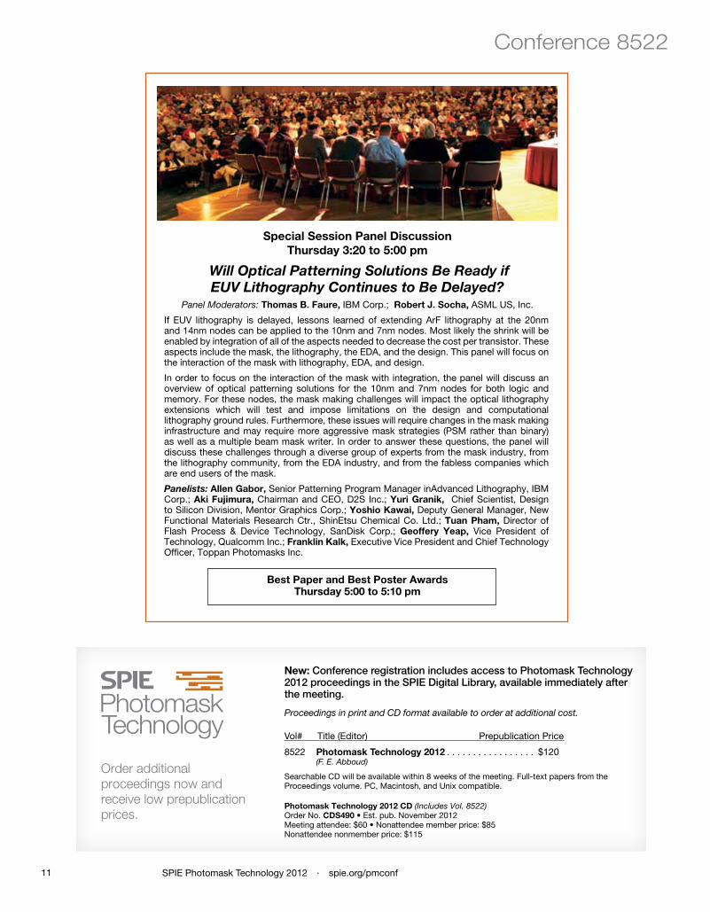
Special.Session.Panel.Discussionthursday.3:20.to.5:00.pm
Will Optical Patterning Solutions Be Ready if EUV Lithography Continues to Be Delayed?
Panel Moderators: thomas.B ..faure, IBM Corp.; Robert.J ..Socha, ASML US, Inc.
If EUV lithography is delayed, lessons learned of extending ArF lithography at the 20nm and 14nm nodes can be applied to the 10nm and 7nm nodes. Most likely the shrink will be enabled by integration of all of the aspects needed to decrease the cost per transistor. These aspects include the mask, the lithography, the EDA, and the design. This panel will focus on the interaction of the mask with lithography, EDA, and design.
In order to focus on the interaction of the mask with integration, the panel will discuss an overview of optical patterning solutions for the 10nm and 7nm nodes for both logic and memory. For these nodes, the mask making challenges will impact the optical lithography extensions which will test and impose limitations on the design and computational lithography ground rules. Furthermore, these issues will require changes in the mask making infrastructure and may require more aggressive mask strategies (PSM rather than binary) as well as a multiple beam mask writer. In order to answer these questions, the panel will discuss these challenges through a diverse group of experts from the mask industry, from the lithography community, from the EDA industry, and from the fabless companies which are end users of the mask.
Panelists: Allen.Gabor, Senior Patterning Program Manager inAdvanced Lithography, IBM Corp.; Aki.fujimura, Chairman and CEO, D2S Inc.; Yuri.Granik, Chief Scientist, Design to Silicon Division, Mentor Graphics Corp.; Yoshio.kawai, Deputy General Manager, New Functional Materials Research Ctr., ShinEtsu Chemical Co. Ltd.; tuan.Pham, Director of Flash Process & Device Technology, SanDisk Corp.; Geoffery. Yeap, Vice President of Technology, Qualcomm Inc.; franklin.kalk, Executive Vice President and Chief Technology Officer, Toppan Photomasks Inc.
Best.Paper.and.Best.Poster.Awards..thursday.5:00.to.5:10.pm
Conference 8522
Vol# Title (Editor) Prepublication Price
8522 Photomask.technology.2012 . . . . . . . . . . . . . . . . . $120 (F. E. Abboud)
Searchable CD will be available within 8 weeks of the meeting. Full-text papers from the Proceedings volume. PC, Macintosh, and Unix compatible.
Photomask.technology.2012.CD.(Includes Vol. 8522)Order No. CDS490 • Est. pub. November 2012Meeting attendee: $60 • Nonattendee member price: $85Nonattendee nonmember price: $115
Order additional proceedings now and receive low prepublication prices.
new: Conference registration includes access to Photomask Technology 2012 proceedings in the SPIE Digital Library, available immediately after the meeting.
Proceedings in print and CD format available to order at additional cost.
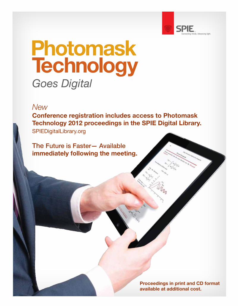
New
Goes Digital
Conference registration includes access to Photomask Technology 2012 proceedings in the SPIE Digital Library.SPIEDigitalLibrary.org The Future is Faster— Available immediately following the meeting.
Proceedings in print and CD format available at additional cost.
Helping engineers and scientists stay current and competitive
DigitalSPIE
LibrarySPIEDigitalLibrary.org
Find the answer
ImagingDefense& Security
SensorsBiomedicalOptics
Astronomy NanophotonicsCommunications Energy