Embed Size (px)
DESCRIPTION
dsacdwa
Citation preview
HARDWARE INTERFACING
LCD AND KEYPAD
INTERFACING
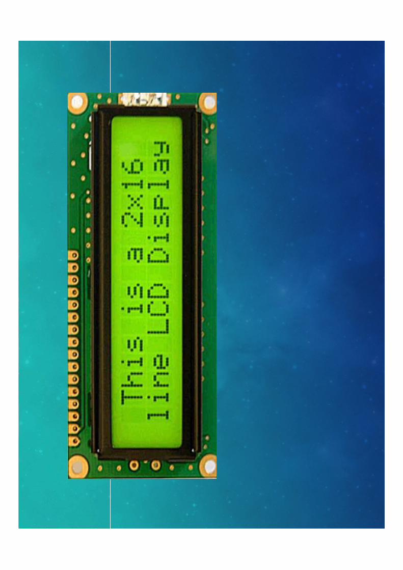
LCD DISPLAY
� This component is specifically manufactured to be used with
microcontrollers, which means that it cannot be activated by
standard IC circuits.
� It is used for displaying different messages on a miniature
liquid crystal display.
� The model described here is for its low price and great
capabilities most frequently used in practice.
� It is based on the HD44780 microcontroller (Hitachi) and can
display messages in two lines with 16 characters each.
� It can display all the letters of alphabet, Greek letters,
punctuation marks, mathematical symbols etc.
� It is also possible to display symbols made up by the user.
� Other useful features include automatic message shift (left
and right), cursor appearance, LED backlight etc.
LCD CONNECTING
� Depending on how many lines are used for connecting an LCD to the
microcontroller, there are 8‐bit and 4‐bit LCD modes.
� The appropriate mode is selected at the beginning of the operation
in the process called 'initialization'.
� The 8‐bit LCD mode uses outputs D0‐ D7 to transfer data as
explained on the previous page.
� The main purpose of the 4‐bit LCD mode is to save valuable I/O pins
of the microcontroller.
� Only 4 higher bits (D4‐D7) are used for communication, while others
may be left unconnected.
� Each piece of data is sent to the LCD in two steps‐ four higher bits
are sent first (normally through the lines D4‐D7), then four lower
bits.
� Initialization enables the LCD to link and interpret received bits
correctly.
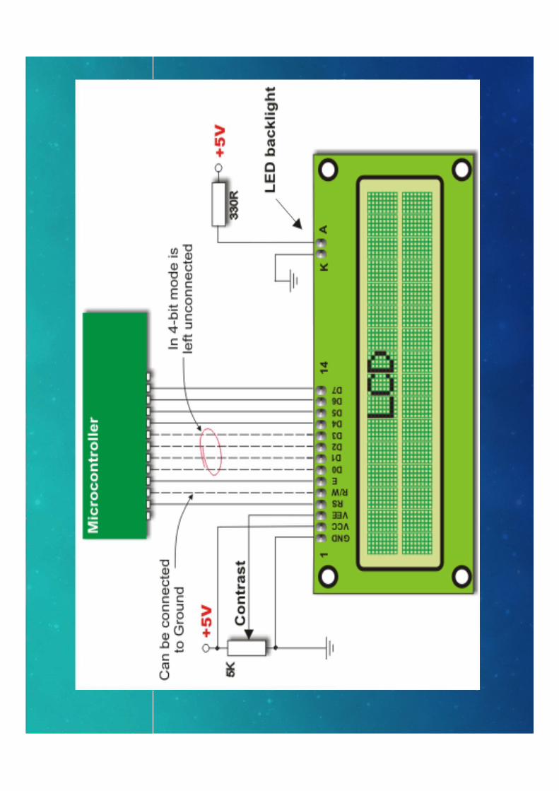
� Data is rarely read from the LCD (it is mainly transferred from
the microcontroller to the LCD) so it is often possible to save
an extra I/O pin by simple connecting the R/W pin to the
Ground.
� Such a saving has its price. Messages will be normally
displayed, but it will not be possible to read the busy flag
since it is not possible to read the display either.
� Fortunately, there is a simple solution. After sending a
character or a command it is important to give the LCD
enough time to do its job.
� Owing to the fact that the execution of a command may last
for approximately 1.64mS, it will be sufficient to wait about
2mS for the LCD.
LCD OPERATION
� In recent years, the LCD has been finding widespread use
replacing LEDs (seven‐segment LEDs or other multisegment
LEDs. This is due to the following reasons:
1. The declining prices of LCDs.
2. The ability to display numbers, characters, and graphics,
this is contrast to LEDs, which are limited to numbers
and a few characters.
3. Incorporation of a refreshing controller into the LCD,
thereby relieving the CPU of the task of refreshing the
LCD. In contrast, the LED must be refreshed by the CPU
(or in some other way) to keep displaying the data.
4. Ease of programming for character and graphics.
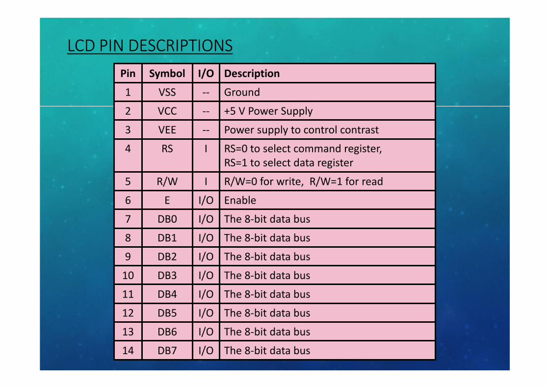
LCD PIN DESCRIPTIONS
Pin Symbol I/O Description
1 VSS ‐‐ Ground
2 VCC ‐‐ +5 V Power Supply
3 VEE ‐‐ Power supply to control contrast
4 RS I RS=0 to select command register,
RS=1 to select data register
5 R/W I R/W=0 for write, R/W=1 for read
6 E I/O Enable
7 DB0 I/O The 8‐bit data bus
8 DB1 I/O The 8‐bit data bus
9 DB2 I/O The 8‐bit data bus
10 DB3 I/O The 8‐bit data bus
11 DB4 I/O The 8‐bit data bus
12 DB5 I/O The 8‐bit data bus
13 DB6 I/O The 8‐bit data bus
14 DB7 I/O The 8‐bit data bus
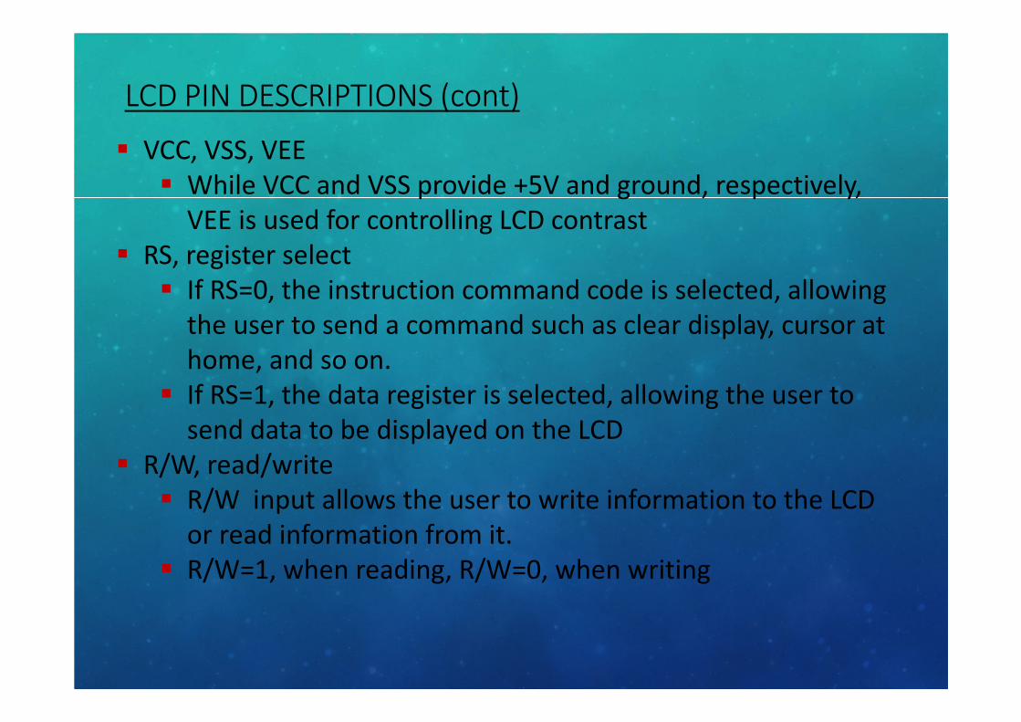
LCD PIN DESCRIPTIONS (cont)
� VCC, VSS, VEE
� While VCC and VSS provide +5V and ground, respectively,
VEE is used for controlling LCD contrast
� RS, register select
� If RS=0, the instruction command code is selected, allowing
the user to send a command such as clear display, cursor at
home, and so on.
� If RS=1, the data register is selected, allowing the user to
send data to be displayed on the LCD
� R/W, read/write
� R/W input allows the user to write information to the LCD
or read information from it.
� R/W=1, when reading, R/W=0, when writing
LCD PIN DESCRIPTIONS (cont)
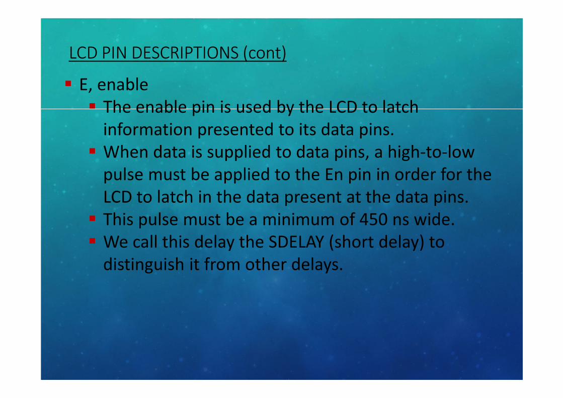
� E, enable
� The enable pin is used by the LCD to latch
information presented to its data pins.
� When data is supplied to data pins, a high‐to‐low
pulse must be applied to the En pin in order for the
LCD to latch in the data present at the data pins.
� This pulse must be a minimum of 450 ns wide.
� We call this delay the SDELAY (short delay) to
distinguish it from other delays.
LCD PIN DESCRIPTIONS (cont)
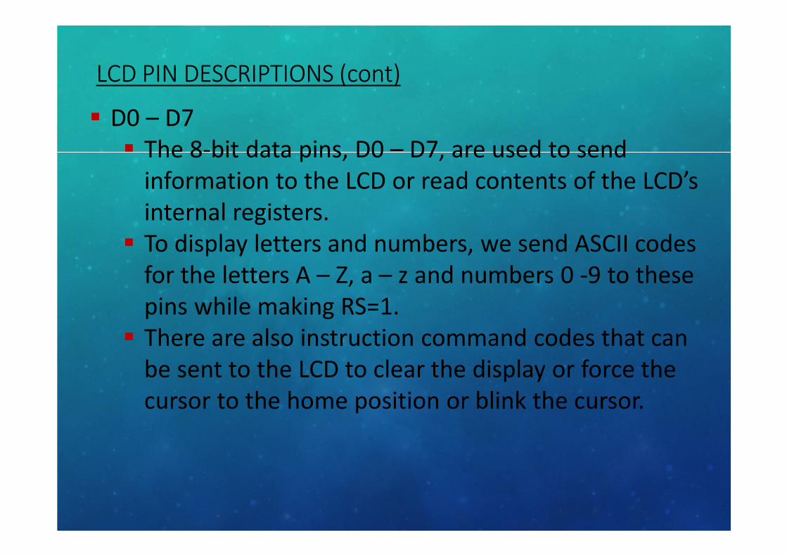
� D0 – D7
� The 8‐bit data pins, D0 – D7, are used to send
information to the LCD or read contents of the LCD’s
internal registers.
� To display letters and numbers, we send ASCII codes
for the letters A – Z, a – z and numbers 0 ‐9 to these
pins while making RS=1.
� There are also instruction command codes that can
be sent to the LCD to clear the display or force the
cursor to the home position or blink the cursor.
LCD PIN DESCRIPTIONS (cont)
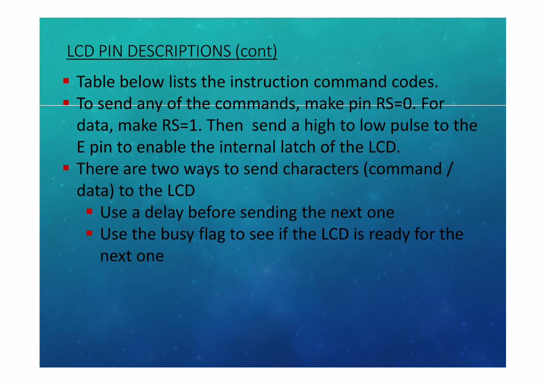
� Table below lists the instruction command codes.
� To send any of the commands, make pin RS=0. For
data, make RS=1. Then send a high to low pulse to the
E pin to enable the internal latch of the LCD.
� There are two ways to send characters (command /
data) to the LCD
� Use a delay before sending the next one
� Use the busy flag to see if the LCD is ready for the
next one
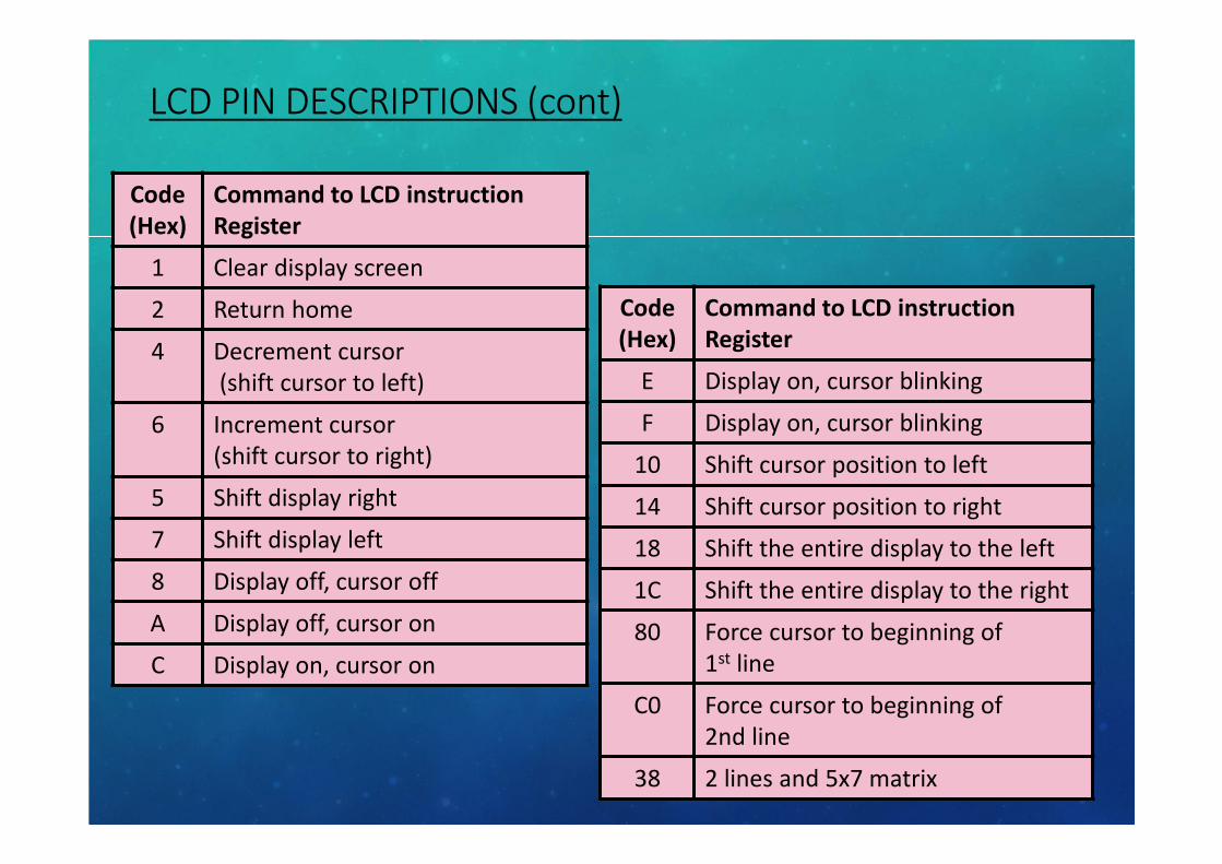
LCD PIN DESCRIPTIONS (cont)
Code
(Hex)
Command to LCD instruction
Register
1 Clear display screen
2 Return home
4 Decrement cursor
(shift cursor to left)
6 Increment cursor
(shift cursor to right)
5 Shift display right
7 Shift display left
8 Display off, cursor off
A Display off, cursor on
C Display on, cursor on
Code
(Hex)
Command to LCD instruction
Register
E Display on, cursor blinking
F Display on, cursor blinking
10 Shift cursor position to left
14 Shift cursor position to right
18 Shift the entire display to the left
1C Shift the entire display to the right
80 Force cursor to beginning of
1st line
C0 Force cursor to beginning of
2nd line
38 2 lines and 5x7 matrix
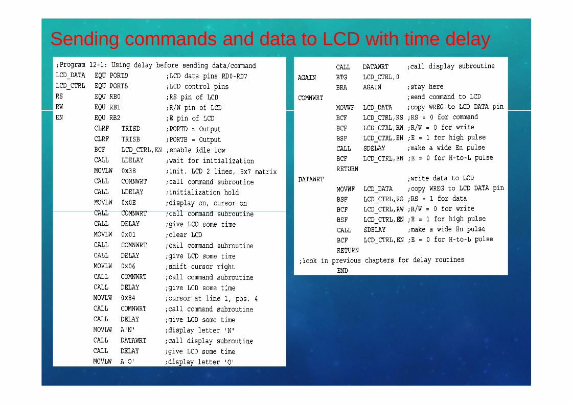
Sending commands and data to LCD with time delay
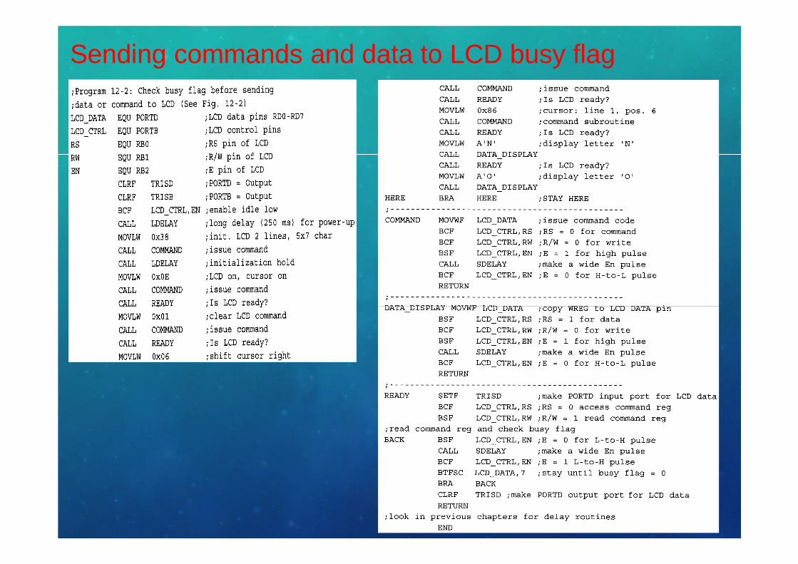
Sending commands and data to LCD busy flag
KEYBOARD INTERFACING
In this sections, we will discuss keyboard fundamental,
along with key press detection and key identification
mechanisms. Then we show how a keyboard is interfaced
to a PIC 18.
MATRIX KEYPAD BASIC OF OPERATION
� Matrix keypads are simply an extension to the simple tact switch
inputs.
� They consists of keys interconnected in the shape of a matrix.
� Each key is a simple mechanical switch located at the crossing
between the matrix rows and columns.
� When a key is pressed, its row and column form an electrical
contact. The rows and columns can be connected to the pins of
microcontroller ports.
� The big advantage of using a matrix keypad is that it allows to
interface a large number of keys with a relatively small number
of microcontroller pins.
� For example, a 16‐key keypad requires only 8 (instead of 16, if
interfaced individually) I/O pins of the microcontroller if
organized into a 4 rows and 4 columns matrix.
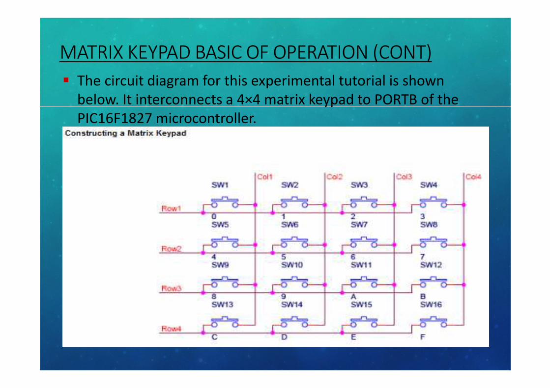
MATRIX KEYPAD BASIC OF OPERATION (CONT)
� The circuit diagram for this experimental tutorial is shown
below. It interconnects a 4×4 matrix keypad to PORTB of the
PIC16F1827 microcontroller.
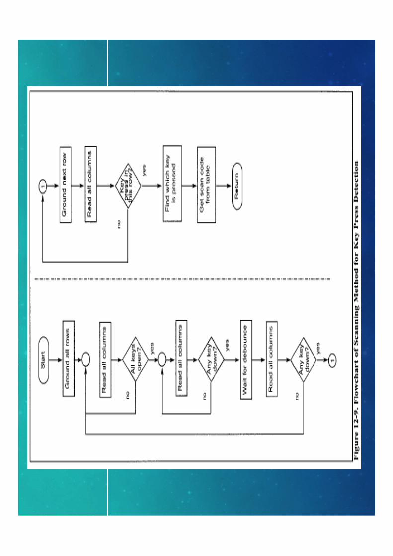
SCANNING A MATRIX KEYPAD
There are many methods depending on how you connect your keypad with your controller, but the basic logic is same. We make the coloums as i/p and we drive the rows making them o/p, this whole procedure of reading the keyboard is called scanning.
In order to detect which key is pressed from the matrix, we make row lines low one by one and read the coloums. Lets say we first make Row1 low, then read the columns. If any of the key in row1 is pressed will make the corrospondingcolumn as low i.e if second key is pressed in Row1, then column2 will give low. So we come to know that key 2 of Row1 is pressed. This is how scanning is done.
So to scan the keypad completely, we need to make rows low one by one and read the columns. If any of the button is pressed in a row, it will take the corrosponding column to a low state which tells us that a key is pressed in that row. If button 1 of a row is pressed then Column 1 will become low, if button 2 then column2 and so on.
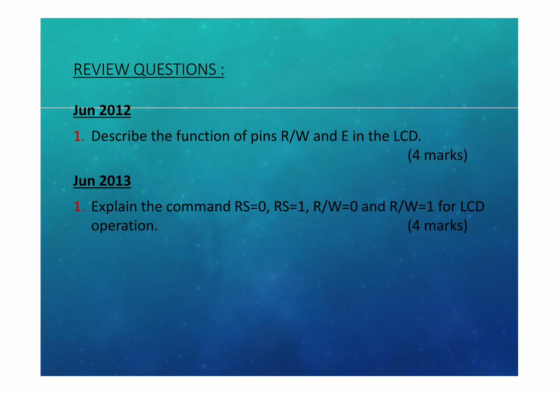
REVIEW QUESTIONS :
Jun 2012
1. Describe the function of pins R/W and E in the LCD.
(4 marks)
Jun 2013
1. Explain the command RS=0, RS=1, R/W=0 and R/W=1 for LCD
operation. (4 marks)

What Lies Behind Us
And What Lies Before Us
Are Tiny Matters
Compared To
What Lies Within Us.