Embed Size (px)
Citation preview
A Physics-Based TCAD Framework for the Noise Analysis of RF CMOS Circuits under theLarge-Signal Operation
Sung-Min Hong, Raseong Kim, Chan Hyeong Park∗, Hong Shick Min, and Young-June ParkSchool of Electrical Engineering and Computer Science and NSI-NCRC,
Seoul National University, Seoul 151-744, KoreaE-mail : [email protected]
∗ School of Electronics Engineering, Kwangwoon University, Seoul 139-701, Korea
Abstract— A general TCAD framework for the large-signal(LS) noise analysis of RF CMOS circuits has been developedemploying an efficient preconditioner for generalized minimalresidual (GMRES) method. In this framework the influence ofthe noise sources inside the devices on the output noise of thecircuit is calculated using the conversion Green’s function (CGF)technique. We expect that the newly-developed TCAD frameworkcan provide a physics-based and efficient LS noise analysis undera mixed device-circuit environment. As an application, noisebehaviors of a single-balanced down-conversion mixer has beensimulated using this framework.
I. I NTRODUCTION
As the technology scaling continues, CMOS has become aviable RF technology for portable wireless systems. In modernwireless communication systems, mixer and local oscillatorcircuits are the key circuits in frequency conversion. Under-standing and analysis of noise performance of these circuitsunder large-signal (LS) conditions has become crucial in thesuccessful low-noise design of CMOS RF ICs. Therefore, weneed an accurate and physics-based TCAD framework fornoise analysis of RF circuits under LS conditions.
In the circuit simulation, many circuit simulators either fortime domain analysis or frequency domain analysis have beendeveloped, based upon the compact MOSFET model (e.g.,SPICE, Agilent ADS, and Cadence SpectreRF), and thesesimulators are widely used for noise analysis of CMOS RFcircuits. However, in the mixed-mode device-circuit simulation[1], only a few attempts have been made to simulate theLS noise behaviors of very simple circuits [2], [3], and westill have to develop more efficient mixed-mode device-circuitsimulators for an accurate LS noise analysis of practical RFCMOS circuits.
In this paper, we report a general TCAD framework of amixed-mode device-circuit solver for the LS noise analysisof RF CMOS circuits. The harmonic balance (HB) method isemployed to solve the state equations, which give the workingpoints of the devices in the circuit considered. The iterativematrix solver, GMRES [4], is adopted as a matrix solver,and an efficient preconditioner, which can be effective evenfor a system with high distortion, is introduced. The paperis organized as follows. Section II is devoted to descriptionof the HB simulation framework, which includes the matrixsolver, GMRES, together with a very efficient preconditionerfor GMRES. In Section III, the conversion Green’s function(CGF) technique, which is employed to calculate the influence
of the noise sources inside the devices on the output noiseof the circuit, is discussed. As an application of our TCADframework, a detailed noise analysis of a single-balanceddown-conversion CMOS RF mixer circuit is presented inSection IV. Conclusions are summarized in Section V.
II. FRAMEWORK FOR THE HARMONIC BALANCE METHOD
We consider a circuit system consisting of semiconductordevices and lumped circuit elements. A lumped circuit elementcan be fully characterized by its terminal voltages and cur-rents. The semiconductor equations (Poisson’s equation andcontinuity equations for electron and hole) for each devicein the circuit are discretized as in the conventional devicesimulators [5]. Then the state variables for the system are theelectric potential, the electron densities and the hole densitiesat every node of the spatially discretized devices, and theterminal voltages and currents of the lumped elements. Thetotal number of the state variables is denoted byNS . Duringthe LS simulation, the noise sources inside the devices andthe lumped elements are not included, and only the responsesof the state variables due to the externally applied voltagesources will be considered. The externally applied voltagescan be time-varying.
In the HB method, we assume that each of the state variablescan be represented as a linear combination ofNH frequencycomponents. From this assumption, each state variable can bedetermined completely from the values of each state variablesat NH sampling times. Now we derive the equations satisfiedby the NSNH values of the state variables atNH samplingtimes. First, we write down theNS state equations for thecircuit system in the time domain, which can be written as
f(x, x) = f1(x) + f2(x)− b = 0, (1)
wheref is the residual vector forNS state variables,x denotesthe vector for the state variables in the time domain,x is thetime derivative ofx, b is the vector for the externally appliedvoltages, andf1 andf2 are usually nonlinear functions. SinceEq. (1) should be satisfied at each ofNH sampling times, wecan constitute from Eq. (1) theNSNH equations satisfied bytheNSNH values of the state variables atNH sampling times,given by
f∗(x∗, x∗) = f∗1 (x∗) + f∗2 (x∗)− b∗ = 0, (2)
119
7-2

wheref∗ is the residual vector for theNSNH state variables,x∗ is the vector for theNSNH values of the state variables,x∗
is the time derivative ofx∗, andb∗ is the vector for the valuesof the external voltages atNH sampling times. LetX be thevector for theNSNH unknown quantities in the frequencydomain corresponding to the vectorx∗, then we have
x∗ = Γ−1X, x∗ = Γ−1ΩX, (3)
whereΓ andΓ−1 are the discrete Fourier transform matrix pairfor x∗ andX, andΩ is a block-diagonal matrix representingthe frequency domain equivalent of the time derivative oper-ation. Substituting Eq. (3) into Eq. (2), we obtain theNSNH
equations satisfied by theNSNH unknown quantities in thefrequency domain.
These equations can be solved by the Newton iterationmethod as follows. LetX0 be a tentative solution for a certainNewton loop and∆ be the correction vector forX0, then∆can be obtained from the following equation of
A1Γ−1Ω∆ + A2Γ−1∆ = −f∗(Γ−1X0, Γ−1ΩX0), (4)
whereA1 and A2 are given by∂f∗1 /∂x∗|0 and ∂f∗2 /∂x∗|0,respectively.A2, which is a matrix with size ofNSNH ×NSNH , is composed ofNH smaller matrixes with size ofNS×NS . Each of theNH smaller matrixes is the quasi-staticJacobian of the system for theNS state variables, evaluatedat each of theNH sampling times. Eq. (4) can be rewritten as
(A1T + A2)δ = −f∗(Γ−1X0, Γ−1ΩX0), (5)
whereT ≡ Γ−1ΩΓ is a matrix representing the time derivativeoperation forx∗ in the time domain,δ ≡ Γ−1∆ is an updatevector in the time domain.
Since the square matrix ofA1T + A2 in Eq. (5) has a sizeof NSNH×NSNH , which is usually too big to be handled bya direct matrix solver such as UMFPACK [6] in the practicalcircuits, we take some efficient approaches [7], [8] to solve Eq.(5) through Krylov subspace method such as GMRES [4] orQMR [9]. In these approaches the most important procedureis to choose an appropriate preconditioner for Eq. (5). Theblock-diagonal preconditioner adopted in [7], [8] has beenknown to be very suitable for a system with low distortion,but this preconditioner is not suitable to a RF circuit wherethe power level is high. In this paper we use the GMRES,and we chooseA2 as a preconditioner because it has beenknown thatA2 can be a very good approximation ofA1T +A2
specially at low frequencies which are much below the cutofffrequencies of the devices in the circuit considered [10] andbecause frequencies of our interest are much below the cutofffrequencies of the MOSFETs in the RF circuit. Since asdiscussed before,A2 is composed ofNH smaller matrixes withsize of NS × NS , each of which is the quasi-static Jacobianof the system for theNS state variables, evaluated at eachof the NH sampling times,A2 can be decomposed intoNH
“small” blocks. These small blocks with size ofNS × NS
can be stored independently. This decomposition will savethe memory usage and the workload for the matrix backsolve
0.6 V + vRF
1.2 V + vLO 1.2 V − vLO
1.8 V
10/0.09 µm
vout+ _
1 kΩ
10/0.09 µm
18/0.09 µm
1 kΩ
0.6 V + vRF
1.2 V + vLO 1.2 V − vLO
1.8 V
10/0.09 µm
vout+ _
1 kΩ
10/0.09 µm
18/0.09 µm
1 kΩ
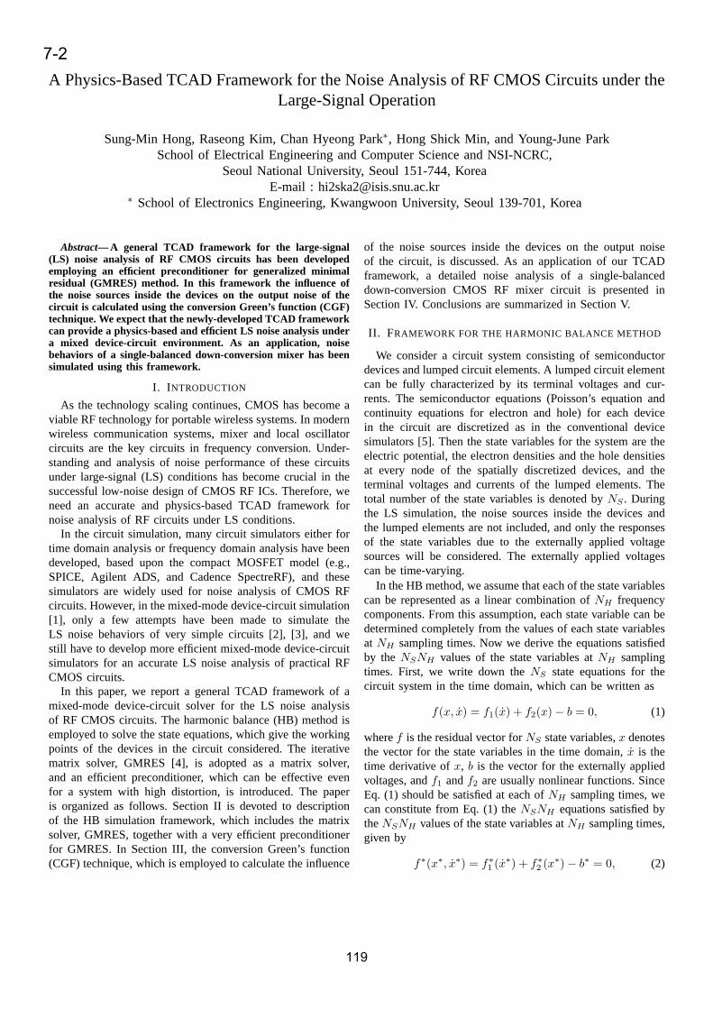
Fig. 1. Circuit schematic of the single-balanced down-conversion mixer.NS
is about 24,000 andNH is set at 21. The LO is a sinusoidal voltage sourceof 1 GHz.
required during the preconditioning process. We expect thatthe time for one GMRES inner solve increases almost linearlyas NH increases. Adoption ofA2 as a preconditioner anddecomposition ofA2 into NH small blocks are distinctivefeatures in our framework. We also note that our solution isexact in the sense that we use the exact Jacobian instead ofan approximate one. Based on the LS working points obtainedthrough the HB method, we will calculate the power spectraldensity of the output noise of the circuit.
III. C ONVERSIONGREEN’ S FUNCTION TECHNIQUE FOR
LARGE-SIGNAL NOISE ANALYSIS
We exploit the conversion Green’s function technique forthe LS noise analysis of the circuit as in [2], [11], [12]. LetGα(r, ω) for α = ψ, n, p be the CGFs for the given outputvariable based on the noiseless working points obtained inSection II as in [2], [11], [12], then the sideband amplitudesof the output noise variables are linearly related to the varioussideband amplitudes of the microscopic noise sources insidethe devices through the CGFs. The sideband correlation matrix(SCM) of two output noise variables, e.g. the short-circuitnoise currents at terminalsi andj, can be written as [2], [11],[12]
Sin,i,in,j(ω) =
∑
α,β=ψ,n,p
∫
Ω
drGα(r, ω)Kγα,γβ(r, ω)G†β(r, ω),
(6)where Kγα,γβ
(r, ω) is the SCM of the local noise sourcesfor spatially uncorrelated microscopic fluctuations,γα denotesthe microscopic noise source included as a forcing term inequationα (α = ψ, n, p denote Poisson’s, electron, and holecontinuity equations, respectively),† denotes the complex con-jugate and transpose, andω is the sideband angular frequency.The direct extension of the generalized adjoint approach [13]allows a numerically efficient evaluation of the CGFs.
IV. SIMULATION RESULTS AND DISCUSSION
Simulation has been carried out on the single-balanceddown-conversion mixer whose output signal is taken as adifferential voltage between the drain terminals of two LOMOSFETs. The circuit schematic considered in the simulation
120

0 1 2 3 4 5 6 7 8 9 1010-7
10-6
10-5
10-4
10-3
10-2
10-1
100
101
Four
ier
coef
ficie
nts
[ V ]
Frequency [ GHz ]
Fig. 2. Magnitudes of Fourier coefficients of the mixer output voltage. Theamplitude of the LO signal is 0.15 V.
0 1 2 3 4 51E-3
0.01
0.1
1
10
Out
put v
olta
ges
[ V ]
RF input frequency [ GHz ]
Fig. 3. Response of the mixer output voltage at 0.1 GHz to the unit RFinput signal at various frequencies.
is shown in Fig. 1. The mixer consists of two resistors andthree nMOSFETs andNS is about 24,000. SinceNH is set at21, the whole system has about half a million unknowns. Theamplitude and frequency of the sinusoidal LO voltage sourceis 0.15 V and 1 GHz, respectively. In the noise calculation,only the diffusion noise sources are considered.
First we perform the LS mixer simulation where only theLO voltage source is imposed. In Fig. 2, the magnitudes ofthe Fourier coefficients of the mixer output voltage are shown.Based upon the simulated LS solution, the response of thelinear periodically time-varying system to the RF input signalis evaluated. We select 0.1 GHz as the sideband frequency.Fig. 3 depicts the response of the mixer output voltage at 0.1GHz due to the unit RF input signal at various frequencies.From this figure, we can see that the conversion gain for the1.1 GHz RF signal is 1.33 V/V.
Let G(r, n) be the CGF due to the noise source in theelectron continuity equation at(n + 0.1) GHz, when theobservation variable is the mixer output noise voltage at 0.1GHz. Fig. 4 showsG(r, 1)’s for the RF port MOSFET andfor the left LO port MOSFET. In the case of the RF portMOSFET, the noise sources in the drain side of the channelgive stronger impact on the mixer output noise. On the otherhand, for the LO port MOSFET the noise sources in the sourceside of the channel have stronger impact on the mixer outputnoise, because in the case of the LO port MOSFET only the
(a)
(b)
Fig. 4. G(r, 1) for (a) the RF port MOSFET and (b) the left LO portMOSFET. G(r, 1) is the CGF due to the noise source in the electroncontinuity equation at 1.1 GHz, when the observation variable is the mixeroutput noise voltage at 0.1 GHz.
noise sources in the source side of the channel go throughthe down-conversion process. Furthermore,G(r, 0) for theLO port MOSFET is shown in Fig. 5. The influence of thenoise source only in the drain side of the LO port MOSFETis found to be dominant because the frequency conversiondoes not take place in this case. Fig. 6 shows magnitudes ofthe diagonal element of the integrand in Eq. (6) at a down-converted frequency (IF frequency) of 0.1 GHz for the leftLO port MOSFET and either for the RF port MOSFET. Thepower spectral density of the mixer output noise voltage iscalculated to be 20.2 (nV)2/Hz, among which 55% comesfrom the RF port MOSFET and the rest comes from the LOport MOSFETs (we neglected the noise from two resistors).Finally, we calculate the mixer output noise voltage at variousLO amplitudes (0.1, 0.15, 0.2, 0.25 V). Fig. 7 shows thesimulated mixer output voltages in the time domain. Also theconversion gains and power spectral densities of the mixeroutput noise voltage are shown in Fig. 8.
V. CONCLUSIONS
In this work, we have developed a general TCAD frame-work for the LS noise analysis of CMOS RF circuits. Thenoise characteristic of the RF CMOS single-balanced down-conversion mixer has been simulated. We expect that this
121

Fig. 5. G(r, 0) for the left LO port MOSFET.
(a)
(b)
Fig. 6. Magnitudes of the diagonal element of the integrand in Eq. (6) at adown-converted frequency (IF frequency) of 0.1 GHz for (a) the left LO portMOSFET and (b) the RF port MOSFET.
0.0 0.2 0.4 0.6 0.8 1.0-0.4
-0.3
-0.2
-0.1
0.0
0.1
0.2
0.3
0.4
0.10 V 0.15 V 0.20 V 0.25 V
v out [
V ]
Time [ nsec ]
Fig. 7. Mixer output voltage in the time domain at various LO amplitudes.
0.05 0.10 0.15 0.20 0.25 0.301.0
1.1
1.2
1.3
1.4
1.5
1.6
LO signal amplitude [ V ]
Con
vers
ion
gain
3.0x10⁻¹⁷
3.2x10⁻¹⁷
3.4x10⁻¹⁷
3.6x10⁻¹⁷
3.8x10⁻¹⁷
4.0x10⁻¹⁷
Po
wer sp
ectra
l density [ V
2 / Hz ]
Fig. 8. Conversion gains and power spectral densities of the mixer outputnoise voltage as a function of the LO amplitude.
framework can be extended for the physics-based and efficientLS noise analysis of general RF CMOS circuits.
ACKNOWLEDGEMENT
This work was supported by the National Core ResearchCenter program of the Korea Science and Engineering Foun-dation (KOSEF) through the NANO Systems Institute at SeoulNational University. C. H. Park’s work was supported by theNational Program for Tera-Level Nanodevices of the Ministryof Science and Technology as one of the 21st century FrontierPrograms.
REFERENCES
[1] J. G. Rollinset al., “Mixed-mode PISCES-SPICE coupled circuit anddevice solver,”IEEE Trans. Computer-Aided Design, vol. 7, pp. 862–867, 1988.
[2] F. Bonani,et al., “A TCAD approach to the physics-based modeling offrequency conversion and noise in semiconductor devices under large-signal forced operation,”IEEE Trans. Electron Devices, vol. 48, pp.966–977, 2001.
[3] J. E. Sanchez,et al., “Two-dimensional semiconductor device simulationof trap-assisted generation-recombination noise under periodic large-signal conditions and its use for developing cyclostationary circuitsimulation models,”IEEE Trans. Electron Devices, vol. 50, pp. 1353–1362, 2003.
[4] Y. Saadet al., “GMRES: a generalized minimal residual method forsolving nonsymmetric linear systems,”SIAM Journal on Scientific andStatistical Computing, vol. 7, pp. 856–869, 1986.
[5] ATLAS Users Manual, SILVACO International, Santa Clara, CA, 2000.[6] T. A. Davis, UMFPACK Version 4.0 User Guide, Dept. of Computer
and Information Science and Engineering, Univ. of Florida, Gainesville,FL, 2002.
[7] B. Troyanovsky, “Frequency domain algorithms for simulating largesignal distortion in semiconductor devices,” Ph.D. dissertation, StanfordUniv., Stanford, CA, 1997.
[8] P. Feldmann,et al., “Efficient frequency domain analysis of largenonlinear analog circuits,” inProc. of IEEE Custom Integrated CircuitsConference, 1996, pp. 461–464.
[9] R. Freund,et al., “Iterative solution of linear systems,”Acta Numerica,pp. 57–100, 1992.
[10] Y. Hu et al., “A comparison of non-quasi-static and quasi-static harmonicbalance implementations for coupled device and circuit simulation,” inProc. of IEEE Custom Integrated Circuits Conference, 2003, pp. 99–102.
[11] F. Bonani,et al., “Physics-based simulation techniques for small- andlarge-signal device noise analysis in RF applications,”IEEE Trans.Electron Devices, vol. 50, pp. 633–644, 2003.
[12] F. Bonaniet al., Noise in Semiconductor Devices. Modeling and Simu-lation. Heidelberg, Germany: Springer-Verlag, 2001.
[13] F. Bonani, et al., “An efficient approach to noise analysis throughmultidimensional physics-based models,”IEEE Trans. Electron Devices,vol. 45, pp. 261–269, 1998.
122