Embed Size (px)
Citation preview

7. Fundamental Transistor Amplifier Configurations
Lecture notes: Sec. 5
Sedra & Smith (6th Ed): Sec. 5.4, 5.6 & 6.3-6.4 Sedra & Smith (5th Ed): Sec. 4.4, 4.6 & 5.3-5.4
ECE 65, Winter2013, F. Najmabadi

Issues in developing a transistor amplifier:
F. Najmabadi, ECE65, Winter 2013, Fundamental Amp Configuration (2/26)
1. Find the iv characteristics of the elements for the signal (which can be different than their characteristics equation for bias). o This will lead to different circuit configurations for bias versus signal
2. Compute circuit response to the signal o Focus on fundamental transistor amplifier configurations
3. How to establish a Bias point (bias is the state of the system when there is no signal). o Stable and robust bias point should be resilient to variations in µnCox (W/L),Vt (or β for BJT) due to temperature and/or manufacturing variability.
o Bias point details impact small signal response (e.g., gain of the amplifier).
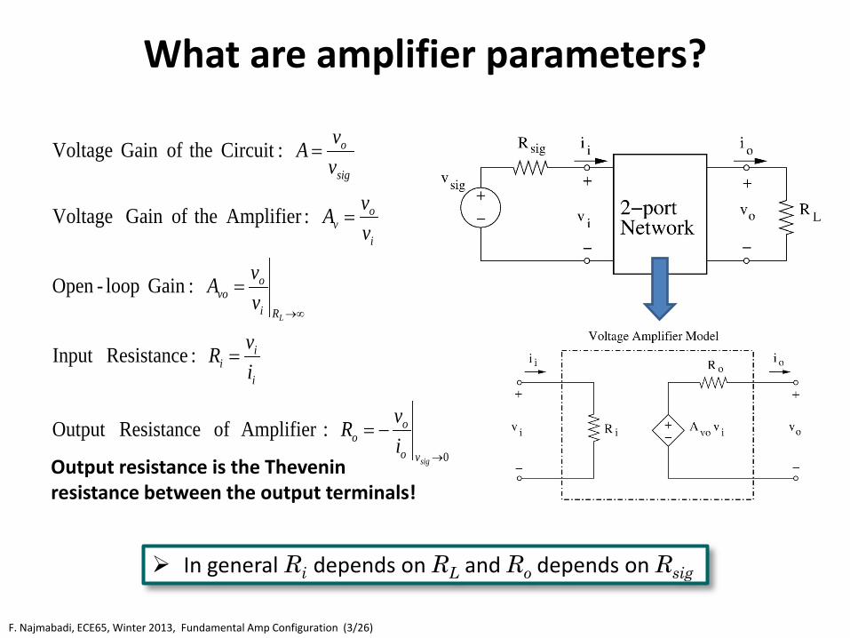
What are amplifier parameters?
F. Najmabadi, ECE65, Winter 2013, Fundamental Amp Configuration (3/26)
:Circuit theofGain Voltage sig
o
vvA =
∞→
=LRi
ovo v
vA :Gain loop-Open
:ResistanceInput i
ii i
vR =
0
: Amplifier of ResistanceOutput →
−=sigvo
oo i
vR
Output resistance is the Thevenin resistance between the output terminals!
:Amplifier theofGain Voltage i
ov v
vA =
In general Ri depends on RL and Ro depends on Rsig
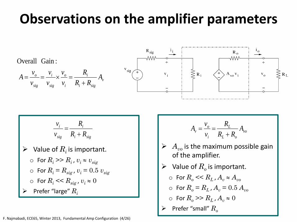
Observations on the amplifier parameters
F. Najmabadi, ECE65, Winter 2013, Fundamental Amp Configuration (4/26)
Avo is the maximum possible gain of the amplifier.
Value of Ro is important. o For Ro << RL , Av ≈ Avo
o For Ro = RL , Av = 0.5 Avo
o For Ro >> RL , Av ≈ 0 Prefer “small” Ro
vooL
L
i
ov A
RRR
vvA
+==
Value of Ri is important. o For Ri >> Ri , vi ≈ vsig
o For Ri = Rsig , vi = 0.5 vsig
o For Ri << Rsig , vi ≈ 0 Prefer “large” Ri
sigi
i
sig
i
RRR
vv
+=
vsigi
i
i
o
sig
i
sig
o ARR
Rvv
vv
vvA
+=×==
:Gain Overall
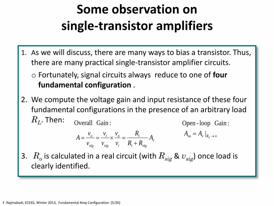
Some observation on single-transistor amplifiers
F. Najmabadi, ECE65, Winter 2013, Fundamental Amp Configuration (5/26)
1. As we will discuss, there are many ways to bias a transistor. Thus, there are many practical single-transistor amplifier circuits.
o Fortunately, signal circuits always reduce to one of four fundamental configuration .
2. We compute the voltage gain and input resistance of these four fundamental configurations in the presence of an arbitrary load RL. Then:
3. Ro is calculated in a real circuit (with Rsig & vsig) once load is clearly identified.
vsigi
i
i
o
sig
i
sig
o ARR
Rvv
vv
vvA
+=×==
:Gain Overall
∞→= | :Gain loop-Open
LRvvo AA
F. Najmabadi, ECE65, Winter 2013, Fundamental Amp Configuration (6/26)
Fundamental Transistor Amplifier Configurations
We are considering only signal circuit here!
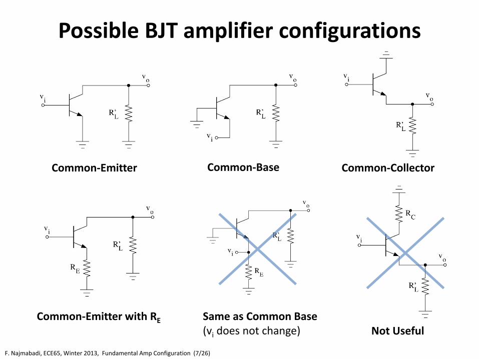
Possible BJT amplifier configurations
F. Najmabadi, ECE65, Winter 2013, Fundamental Amp Configuration (7/26)
Same as Common Base (vi does not change)
Common-Base Common-Collector
Common-Emitter with RE
Not Useful
Common-Emitter
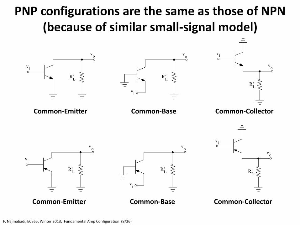
PNP configurations are the same as those of NPN (because of similar small-signal model)
F. Najmabadi, ECE65, Winter 2013, Fundamental Amp Configuration (8/26)
Common-Base Common-Collector Common-Emitter
Common-Emitter Common-Base Common-Collector
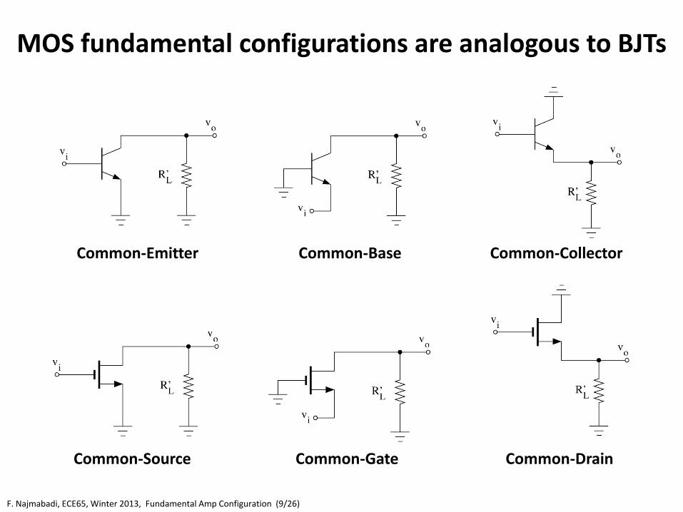
MOS fundamental configurations are analogous to BJTs
F. Najmabadi, ECE65, Winter 2013, Fundamental Amp Configuration (9/26)
Common-Base Common-Collector Common-Emitter
Common-Source Common-Gate Common-Drain
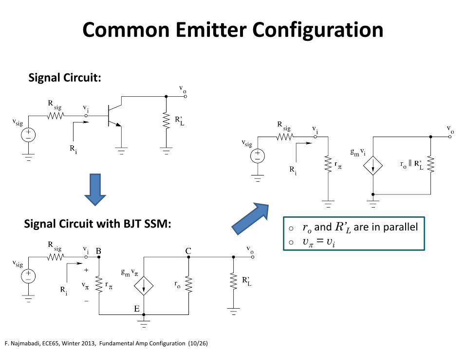
Common Emitter Configuration
F. Najmabadi, ECE65, Winter 2013, Fundamental Amp Configuration (10/26)
Signal Circuit:
Signal Circuit with BJT SSM: o ro and R’L are in parallel o vπ = vi
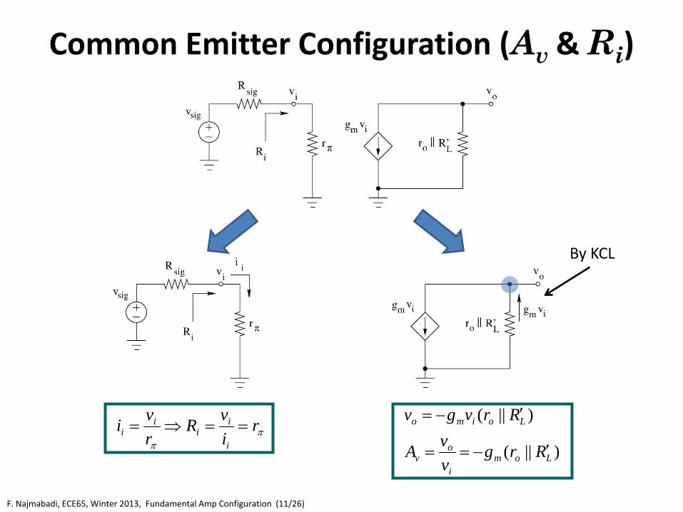
Common Emitter Configuration (Av & Ri)
F. Najmabadi, ECE65, Winter 2013, Fundamental Amp Configuration (11/26)
ππ
rivR
rvi
i
ii
ii ==⇒=
)||(
)||(
Lomi
ov
Loimo
RrgvvA
Rrvgv
′−==
′−=
By KCL
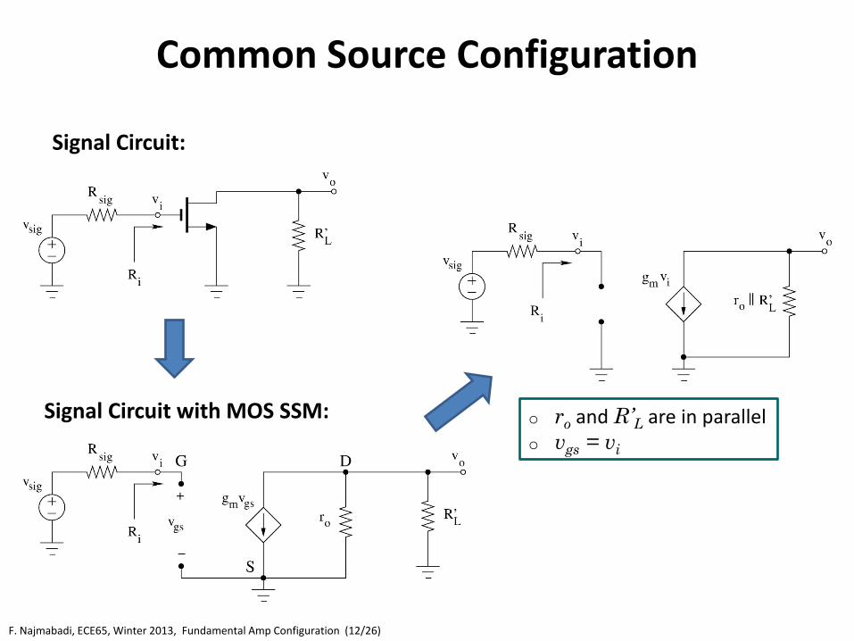
Common Source Configuration
F. Najmabadi, ECE65, Winter 2013, Fundamental Amp Configuration (12/26)
Signal Circuit:
Signal Circuit with MOS SSM: o ro and R’L are in parallel o vgs = vi
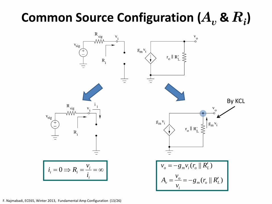
Common Source Configuration (Av & Ri)
F. Najmabadi, ECE65, Winter 2013, Fundamental Amp Configuration (13/26)
0 ∞==⇒=i
iii i
vRi )||(
)||(
Lomi
ov
Loimo
RrgvvA
Rrvgv
′−==
′−=
By KCL
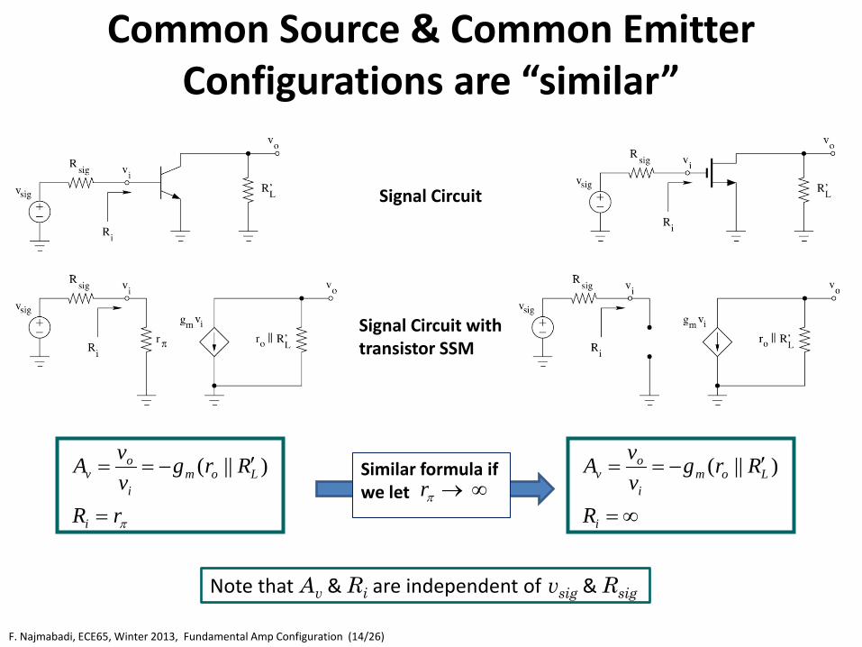
Common Source & Common Emitter Configurations are “similar”
F. Najmabadi, ECE65, Winter 2013, Fundamental Amp Configuration (14/26)
Signal Circuit
Signal Circuit with transistor SSM
)||(
πrR
RrgvvA
i
Lomi
ov
=
′−==
)||(
∞=
′−==
i
Lomi
ov
R
RrgvvASimilar formula if
we let ∞→ πr
Note that Av & Ri are independent of vsig & Rsig

Common Emitter Configuration with RE
F. Najmabadi, ECE65, Winter 2013, Fundamental Amp Configuration (15/26)
Signal Circuit:
Signal Circuit with BJT SSM:
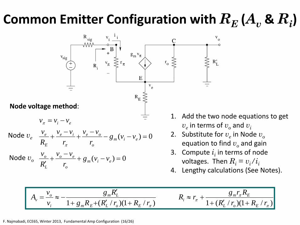
Common Emitter Configuration with RE (Av & Ri)
F. Najmabadi, ECE65, Winter 2013, Fundamental Amp Configuration (16/26)
)/1)(/(1
)/1)(/(1
π
ππ
π rRrRRrgrR
rRrRRgRg
vvA
EoL
Emi
EoLEm
Lm
i
ov +′+
+≈+′++
′−≈=
0)(
0)(
=−+−
+′
=−−−
+−
+
−=
eimo
eo
L
o
eimo
oeie
E
e
ei
vvgr
vvRv
vvgr
vvr
vvRv
vvv
π
π
Node voltage method:
Node ve
Node vo
1. Add the two node equations to get ve in terms of vo and vi
2. Substitute for ve in Node vo equation to find vo and gain
3. Compute ii in terms of node voltages. Then Ri = vi/ii
4. Lengthy calculations (See Notes).
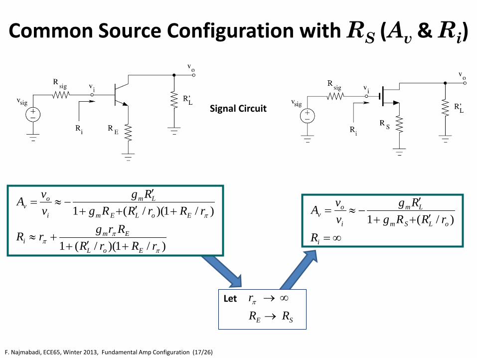
Common Source Configuration with RS (Av & Ri)
F. Najmabadi, ECE65, Winter 2013, Fundamental Amp Configuration (17/26)
Signal Circuit
Let
SE RRr
→∞→π
)/1)(/(1
)/1)(/(1
π
ππ
π
rRrRRrgrR
rRrRRgRg
vvA
EoL
Emi
EoLEm
Lm
i
ov
+′++≈
+′++′
−≈=
∞=
′++′
−≈=
i
oLSm
Lm
i
ov
RrRRg
RgvvA
)/(1
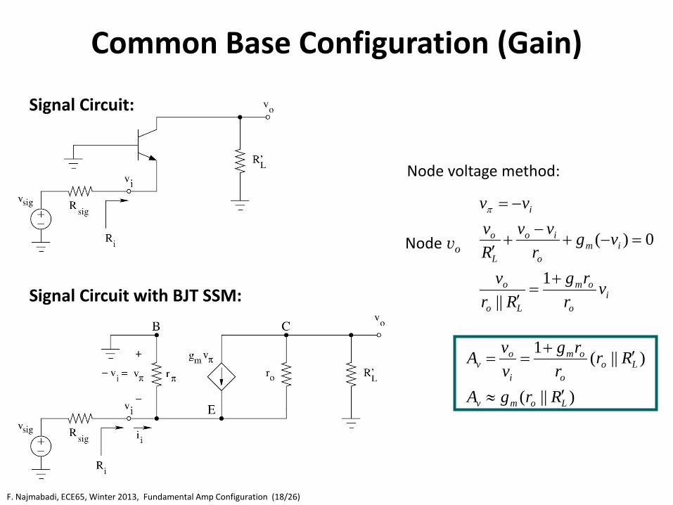
Common Base Configuration (Gain)
F. Najmabadi, ECE65, Winter 2013, Fundamental Amp Configuration (18/26)
Signal Circuit:
Signal Circuit with BJT SSM:
)||(
)||(1
Lomv
Loo
om
i
ov
RrgA
Rrr
rgvvA
′≈
′+==
io
om
Lo
o
imo
io
L
o
i
vr
rgRr
v
vgr
vvRv
vv
+=
′
=−+−
+′
−=
1||
0)(
π
Node voltage method:
Node vo
Common Base Configuration (Ri)
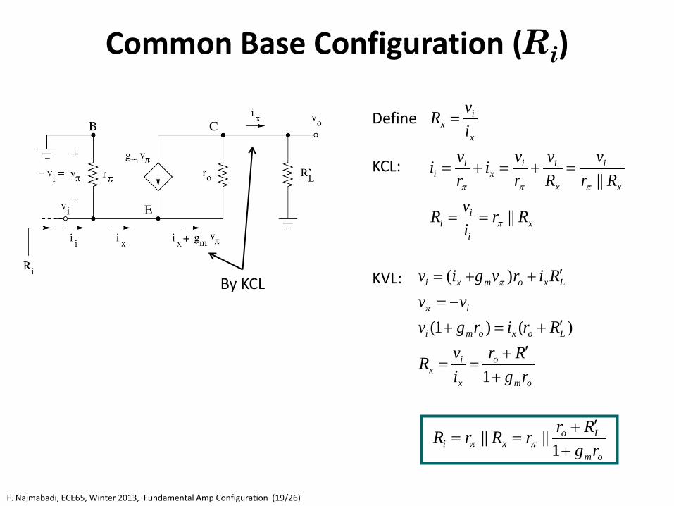
F. Najmabadi, ECE65, Winter 2013, Fundamental Amp Configuration (19/26)
1
|||| om
Loxi rg
RrrRrR+
′+== ππ
om
o
x
ix
Loxomi
i
Lxomxi
rgRr
ivR
Rrirgvvv
Rirvgiv
+′+
==
′+=+−=
′++=
1
)()1(
)(
π
πKVL:
xi
ii
x
i
x
iix
ii
x
ix
RrivR
Rrv
Rv
rvi
rvi
ivR
||
||
π
πππ
==
=+=+=
=Define
KCL:
By KCL
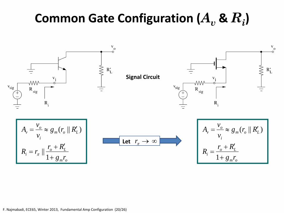
Common Gate Configuration (Av & Ri)
F. Najmabadi, ECE65, Winter 2013, Fundamental Amp Configuration (20/26)
Signal Circuit
1
||
)||(
om
Loi
Lomi
ov
rgRrrR
RrgvvA
+′+
=
′≈=
π
Let ∞→ πr
1
)||(
om
Loi
Lomi
ov
rgRrR
RrgvvA
+′+
=
′≈=
Common Collector Configuration (Emitter Follower)
F. Najmabadi, ECE65, Winter 2013, Fundamental Amp Configuration (21/26)
Signal Circuit:
Signal Circuit with BJT SSM:
)||(1
)||( Lom
Lom
i
ov Rrg
RrgvvA
′+′
==
imim
momLo
o
oimo
oio
L
o
oi
vgvrg
gvrgRr
v
vvgrv
rvv
Rv
vvv
≈
+=
++
′
=−−+−
+′
−=
ππ
π
π
1111||
0)(
Node voltage method:
Node vo
1>>= βπrgm
vi
ii
vioi
i
Ar
ivR
Arv
rvvi
−==
−×=−
=
1
)1(
π
ππ
)||()||( LoLomi RrrRrrgrR ′+=′+= βπππ
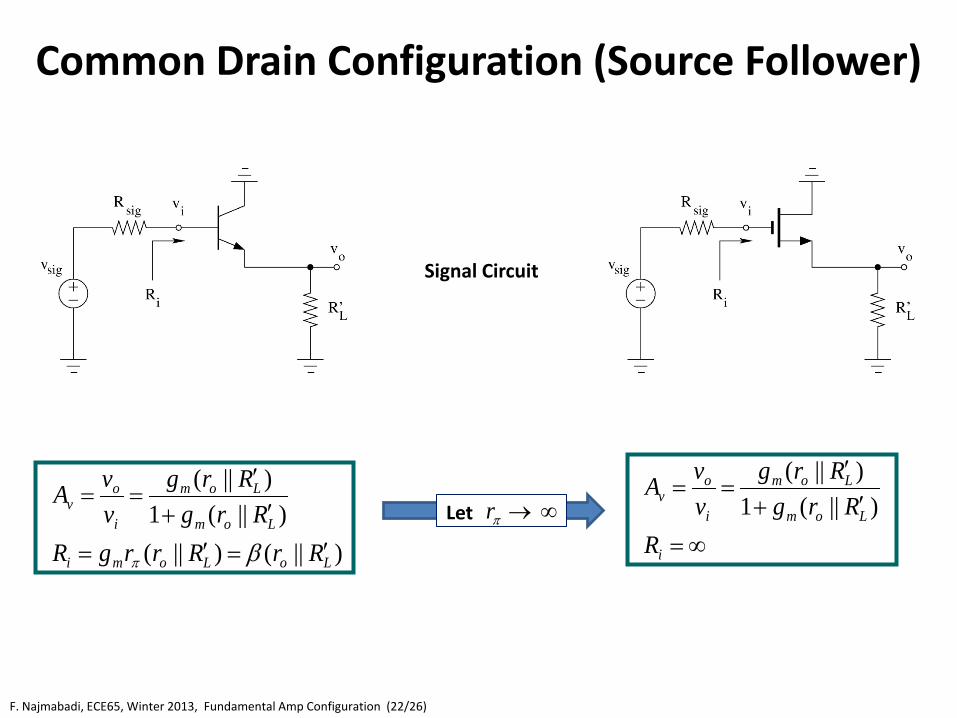
Common Drain Configuration (Source Follower)
F. Najmabadi, ECE65, Winter 2013, Fundamental Amp Configuration (22/26)
Signal Circuit
)||()||(
)||(1
)||(
LoLomi
Lom
Lom
i
ov
RrRrrgRRrg
RrgvvA
′=′=
′+′
==
βπ
Let ∞→ πr∞=
′+′
==
i
Lom
Lom
i
ov
RRrg
RrgvvA
)||(1
)||(
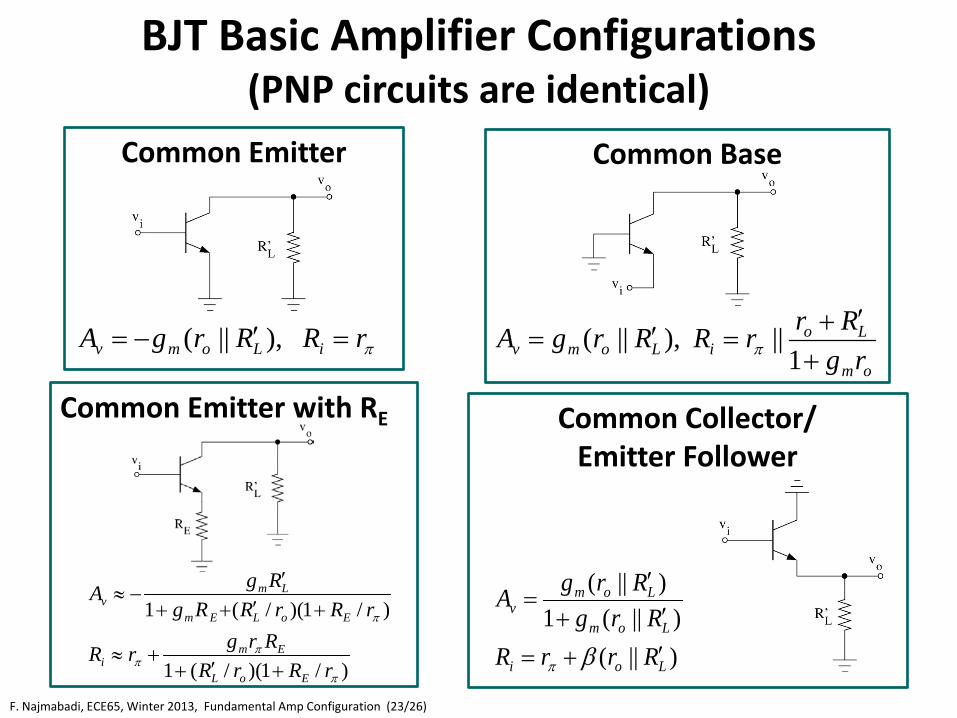
BJT Basic Amplifier Configurations (PNP circuits are identical)
F. Najmabadi, ECE65, Winter 2013, Fundamental Amp Configuration (23/26)
Common Emitter ),||( πrRRrgA iLomv =′−=
Common Base
om
LoiLomv rg
RrrRRrgA+
′+=′=
1|| ),||( π
Common Collector/ Emitter Follower
)||(
)||(1
)||(
Loi
Lom
Lomv
RrrRRrg
RrgA
′+=
′+′
=
βπ)/1)(/(1
)/1)(/(1
π
ππ
π
rRrRRrgrR
rRrRRgRgA
EoL
Emi
EoLEm
Lmv
+′++≈
+′++′
−≈
Common Emitter with RE

MOS Basic Amplifier Configurations (PMOS circuits are identical)
F. Najmabadi, ECE65, Winter 2013, Fundamental Amp Configuration (24/26)
Common Source with RS ,
/1∞=
′++′
−= ioLSm
Lmv R
rRRgRgA
Common Drain/Source Follower
,)||(1
)||(∞=
′+′
= iLom
Lomv R
RrgRrgA
),||( ∞=′−= iLomv RRrgA
Common Source
Common Gate
om
LoiLomv rg
RrRRrgA+
′+=′=
1 ),||(
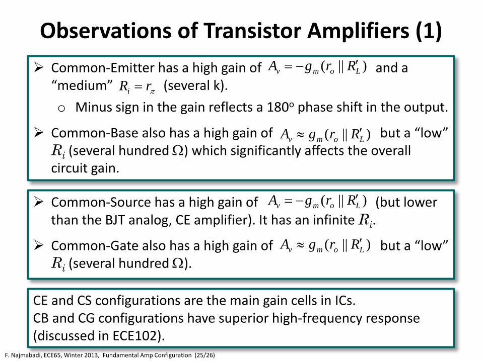
Observations of Transistor Amplifiers (1)
F. Najmabadi, ECE65, Winter 2013, Fundamental Amp Configuration (25/26)
Common-Emitter has a high gain of and a “medium” (several k).
o Minus sign in the gain reflects a 180o phase shift in the output.
Common-Base also has a high gain of but a “low” Ri (several hundred Ω) which significantly affects the overall circuit gain.
)||( Lomv RrgA ′−= πrRi =
)||( Lomv RrgA ′≈
Common-Source has a high gain of (but lower than the BJT analog, CE amplifier). It has an infinite Ri.
Common-Gate also has a high gain of but a “low” Ri (several hundred Ω).
)||( Lomv RrgA ′−=
)||( Lomv RrgA ′≈
CE and CS configurations are the main gain cells in ICs. CB and CG configurations have superior high-frequency response (discussed in ECE102).
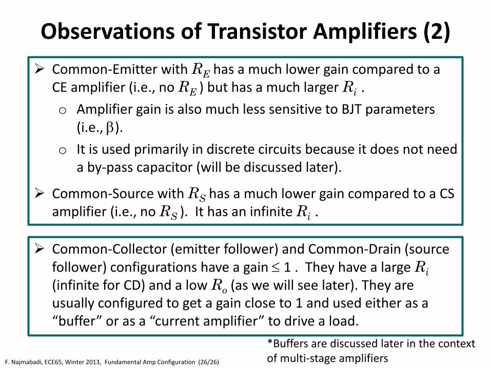
Observations of Transistor Amplifiers (2)
F. Najmabadi, ECE65, Winter 2013, Fundamental Amp Configuration (26/26)
Common-Emitter with RE has a much lower gain compared to a CE amplifier (i.e., no RE ) but has a much larger Ri . o Amplifier gain is also much less sensitive to BJT parameters
(i.e., β).
o It is used primarily in discrete circuits because it does not need a by-pass capacitor (will be discussed later).
Common-Source with RS has a much lower gain compared to a CS amplifier (i.e., no RS ). It has an infinite Ri .
Common-Collector (emitter follower) and Common-Drain (source follower) configurations have a gain ≤ 1 . They have a large Ri (infinite for CD) and a low Ro (as we will see later). They are usually configured to get a gain close to 1 and used either as a “buffer” or as a “current amplifier” to drive a load.
*Buffers are discussed later in the context of multi-stage amplifiers


![RF Circuit Design - [Ch4-1] Microwave Transistor Amplifier](https://img.pdfslide.net/doc/110x75/55cc6094bb61eb9d338b474f/rf-circuit-design-ch4-1-microwave-transistor-amplifier.jpg)