Embed Size (px)
Citation preview
DS180 (v1.0) June 21, 2010 www.xilinx.comAdvance Product Specification 1
© Copyright 2010 Xilinx, Inc. XILINX, the Xilinx logo, Virtex, Spartan, ISE, and other designated brands included herein are trademarks of Xilinx in the United States and other countries. PCI Express is a trademark of PCI-SIG and used under license. All other trademarks are the property of their respective owners.
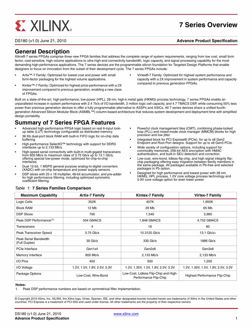
General DescriptionXilinx® 7 series FPGAs comprise three new FPGA families that address the complete range of system requirements, ranging from low cost, small form factor, cost-sensitive, high-volume applications to ultra high-end connectivity bandwidth, logic capacity, and signal processing capability for the most demanding high-performance applications. The 7 series devices are the programmable silicon foundation for Targeted Design Platforms that enable designers to focus on innovation from the outset of their development cycle. The 7 series FPGAs include:
• Artix™-7 Family: Optimized for lowest cost and power with small form-factor packaging for the highest volume applications.
• Kintex™-7 Family: Optimized for highest price-performance with a 2X improvement compared to previous generation, enabling a new class of FPGAs.
• Virtex®-7 Family: Optimized for highest system performance and capacity with a 2X improvement in system performance and capacity compared to previous generation FPGAs.
Built on a state-of-the-art, high-performance, low-power (HPL), 28 nm, high-k metal gate (HKMG) process technology, 7 series FPGAs enable an unparalleled increase in system performance with 2.4 Tb/s of I/O bandwidth, 2 million logic cell capacity, and 4.7 TMACS DSP, while consuming 50% less power than previous generation devices to offer a fully programmable alternative to ASSPs and ASICs. All 7 series devices share a unified fourth-generation Advanced Silicon Modular Block (ASMBL™) column-based architecture that reduces system development and deployment time with simplified design portability.
Summary of 7 Series FPGA Features• Advanced high-performance FPGA logic based on real 6-input look-
up table (LUT) technology configurable as distributed memory.• 36 Kb dual-port block RAM with built-in FIFO logic for on-chip data
buffering.• High-performance SelectIO™ technology with support for DDR3
interfaces up to 2,133 Mb/s.• High-speed serial connectivity with built-in multi-gigabit transceivers
from 600 Mb/s to maximum rates of 3.75 Gb/s up to 13.1 Gb/s, offering special low-power mode, optimized for chip-to-chip interfaces.
• Dual 12-bit, 1 MSPS general purpose analog-to-digital converters (XADC) with on-chip temperature and power supply sensors.
• DSP slices with 25 x 18 multiplier, 48-bit accumulator, and pre-adder for high performance filtering, including optimized symmetric coefficient filtering.
• Powerful clock management tiles (CMT), combining phase-locked loop (PLL) and mixed-mode clock manager (MMCM) blocks for high precision and low jitter.
• Integrated block for PCI Express® (PCIe), for up to x8 Gen2 Endpoint and Root Port designs. Support for up to x8 Gen3 PCIe.
• Wide variety of configuration options, including support for commodity memories, 256-bit AES encryption with HMAC authentication, and built-in SEU detection and correction.
• Low-cost, wire-bond, lidless flip-chip, and high signal integrity flip-chip packaging offering easy migration between family members in the same package. All packages available in Pb-free and selected packages in Pb option.
• Designed for high performance and lowest power with 28 nm, HKMG, HPL process, 1.0V core voltage process technology and 0.9V core voltage option for even lower power.
12
7 Series Overview
DS180 (v1.0) June 21, 2010 Advance Product Specification
Table 1: 7 Series Families Comparison
Maximum Capability Artix-7 Family Kintex-7 Family Virtex-7 Family
Logic Cells 352K 407K 1,955K
Block RAM 12 Mb 29 Mb 65 Mb
DSP Slices 700 1,540 3,960
Peak DSP Performance(1) 504 GMACS 1,848 GMACS 4,752 GMACS
Transceivers 4 16 80
Peak Transceiver Speed 3.75 Gb/s 10.3125 Gb/s 13.1 Gb/s+
Peak Serial Bandwidth (Full Duplex) 30 Gb/s 330 Gb/s 1886 Gb/s
PCIe Interface Gen1x4 Gen2x8 Gen3x8
Memory Interface 800 Mb/s 2,133 Mb/s 2,133 Mb/s
I/O Pins 450 500 1,200
I/O Voltage 1.2V, 1.5V, 1.8V, 2.5V, 3.3V 1.2V, 1.35V, 1.5V, 1.8V, 2.5V, 3.3V 1.2V, 1.35V, 1.5V, 1.8V, 2.5V, 3.3V
Package Options Low-Cost, Wire-BondLow-Cost, Lidless Flip-Chip and High-
Performance Flip-ChipHighest Performance Flip-Chip
Notes: 1. Peak DSP performance numbers are based on symmetrical filter implementation.
7 Series Overview
DS180 (v1.0) June 21, 2010 www.xilinx.comAdvance Product Specification 2
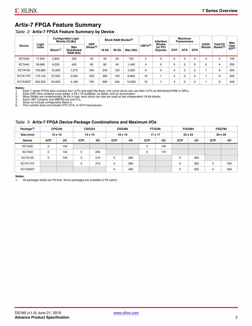
Artix-7 FPGA Feature SummaryTable 2: Artix-7 FPGA Feature Summary by Device
Device Logic Cells
Configurable Logic Blocks (CLBs)
DSP Slices(2)
Block RAM Blocks(3)
CMTs(4)
Interface Blocks for PCI
Express
Maximum Transceivers
XADC Blocks
Total I/O Banks(5)
Max User I/O(6)
Slices(1)Max
Distributed RAM (Kb)
18 Kb 36 Kb Max (Kb) GTP GTX GTH
XC7A20 17,920 2,800 225 40 40 20 720 2 0 0 0 0 0 2 100
XC7A40 39,680 6,200 450 80 80 40 1,440 4 0 0 0 0 0 4 200
XC7A105 103,680 16,200 1,275 240 240 120 4,320 6 0 0 0 0 1 6 300
XC7A175T 173,120 27,050 2,063 400 390 195 6,600 10 1 4 0 0 1 9 450
XC7A355T 352,320 55,050 4,188 700 690 345 12,060 10 1 4 0 0 1 9 450
Notes: 1. Each 7 series FPGA slice contains four LUTs and eight flip-flops; only some slices can use their LUTs as distributed RAM or SRLs.2. Each DSP slice contains a pre-adder, a 25 x 18 multiplier, an adder, and an accumulator.3. Block RAMs are fundamentally 36 Kb in size; each block can also be used as two independent 18 Kb blocks.4. Each CMT contains one MMCM and one PLL.5. Does not include configuration Bank 0.6. This number does not include GTP, GTX, or GTH transceivers.
Table 3: Artix-7 FPGA Device-Package Combinations and Maximum I/Os
Package(1) CPG236 CSG324 CSG484 FTG256 FGG484 FGG784
Size (mm) 10 x 10 15 x 15 19 x 19 17 x 17 23 x 23 29 x 29
Device GTP I/O GTP I/O GTP I/O GTP I/O GTP I/O GTP I/O
XC7A20 0 100 0 100
XC7A40 0 140 0 200 0 170
XC7A105 0 140 0 210 0 285 0 300
XC7A175T 0 210 4 285 0 325 4 450
XC7A355T 4 285 0 325 4 450
Notes: 1. All packages listed are Pb-free. Some packages are available in Pb option.
7 Series Overview
DS180 (v1.0) June 21, 2010 www.xilinx.comAdvance Product Specification 3
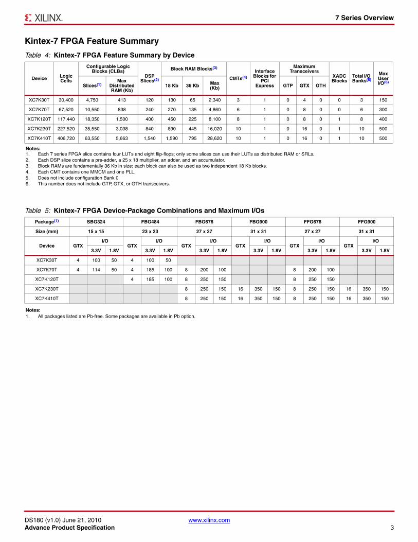
Kintex-7 FPGA Feature Summary
Table 4: Kintex-7 FPGA Feature Summary by Device
Device Logic Cells
Configurable Logic Blocks (CLBs)
DSP Slices(2)
Block RAM Blocks(3)
CMTs(4)
Interface Blocks for
PCI Express
Maximum Transceivers
XADC Blocks
Total I/O Banks(5)
Max User I/O(6)
Slices(1)Max
Distributed RAM (Kb)
18 Kb 36 Kb Max (Kb) GTP GTX GTH
XC7K30T 30,400 4,750 413 120 130 65 2,340 3 1 0 4 0 0 3 150
XC7K70T 67,520 10,550 838 240 270 135 4,860 6 1 0 8 0 0 6 300
XC7K120T 117,440 18,350 1,500 400 450 225 8,100 8 1 0 8 0 1 8 400
XC7K230T 227,520 35,550 3,038 840 890 445 16,020 10 1 0 16 0 1 10 500
XC7K410T 406,720 63,550 5,663 1,540 1,590 795 28,620 10 1 0 16 0 1 10 500
Notes: 1. Each 7 series FPGA slice contains four LUTs and eight flip-flops; only some slices can use their LUTs as distributed RAM or SRLs.2. Each DSP slice contains a pre-adder, a 25 x 18 multiplier, an adder, and an accumulator.3. Block RAMs are fundamentally 36 Kb in size; each block can also be used as two independent 18 Kb blocks.4. Each CMT contains one MMCM and one PLL.5. Does not include configuration Bank 0.6. This number does not include GTP, GTX, or GTH transceivers.
Table 5: Kintex-7 FPGA Device-Package Combinations and Maximum I/Os
Package(1) SBG324 FBG484 FBG676 FBG900 FFG676 FFG900
Size (mm) 15 x 15 23 x 23 27 x 27 31 x 31 27 x 27 31 x 31
Device GTXI/O
GTXI/O
GTXI/O
GTXI/O
GTXI/O
GTXI/O
3.3V 1.8V 3.3V 1.8V 3.3V 1.8V 3.3V 1.8V 3.3V 1.8V 3.3V 1.8V
XC7K30T 4 100 50 4 100 50
XC7K70T 4 114 50 4 185 100 8 200 100 8 200 100
XC7K120T 4 185 100 8 250 150 8 250 150
XC7K230T 8 250 150 16 350 150 8 250 150 16 350 150
XC7K410T 8 250 150 16 350 150 8 250 150 16 350 150
Notes: 1. All packages listed are Pb-free. Some packages are available in Pb option.
7 Series Overview
DS180 (v1.0) June 21, 2010 www.xilinx.comAdvance Product Specification 4
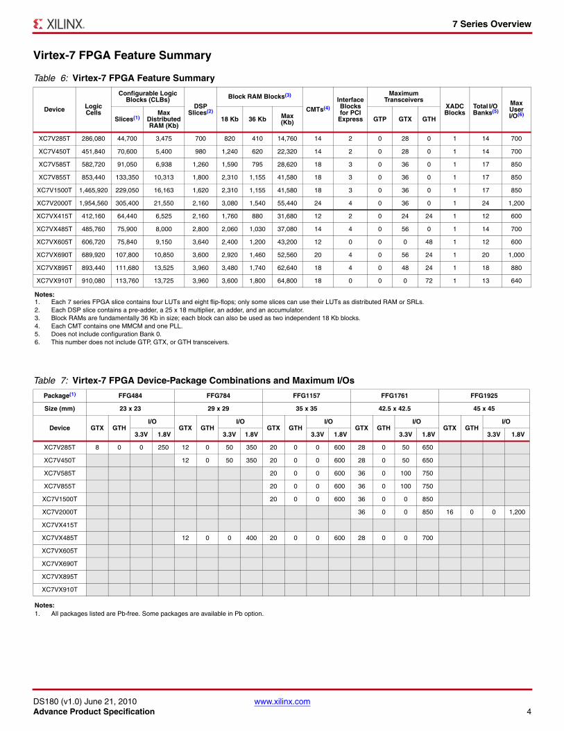
Virtex-7 FPGA Feature Summary
Table 6: Virtex-7 FPGA Feature Summary
Device Logic Cells
Configurable Logic Blocks (CLBs)
DSP Slices(2)
Block RAM Blocks(3)
CMTs(4)
Interface Blocks for PCI
Express
Maximum Transceivers
XADC Blocks
Total I/O Banks(5)
Max User I/O(6)
Slices(1)Max
Distributed RAM (Kb)
18 Kb 36 Kb Max (Kb) GTP GTX GTH
XC7V285T 286,080 44,700 3,475 700 820 410 14,760 14 2 0 28 0 1 14 700
XC7V450T 451,840 70,600 5,400 980 1,240 620 22,320 14 2 0 28 0 1 14 700
XC7V585T 582,720 91,050 6,938 1,260 1,590 795 28,620 18 3 0 36 0 1 17 850
XC7V855T 853,440 133,350 10,313 1,800 2,310 1,155 41,580 18 3 0 36 0 1 17 850
XC7V1500T 1,465,920 229,050 16,163 1,620 2,310 1,155 41,580 18 3 0 36 0 1 17 850
XC7V2000T 1,954,560 305,400 21,550 2,160 3,080 1,540 55,440 24 4 0 36 0 1 24 1,200
XC7VX415T 412,160 64,440 6,525 2,160 1,760 880 31,680 12 2 0 24 24 1 12 600
XC7VX485T 485,760 75,900 8,000 2,800 2,060 1,030 37,080 14 4 0 56 0 1 14 700
XC7VX605T 606,720 75,840 9,150 3,640 2,400 1,200 43,200 12 0 0 0 48 1 12 600
XC7VX690T 689,920 107,800 10,850 3,600 2,920 1,460 52,560 20 4 0 56 24 1 20 1,000
XC7VX895T 893,440 111,680 13,525 3,960 3,480 1,740 62,640 18 4 0 48 24 1 18 880
XC7VX910T 910,080 113,760 13,725 3,960 3,600 1,800 64,800 18 0 0 0 72 1 13 640
Notes: 1. Each 7 series FPGA slice contains four LUTs and eight flip-flops; only some slices can use their LUTs as distributed RAM or SRLs.2. Each DSP slice contains a pre-adder, a 25 x 18 multiplier, an adder, and an accumulator.3. Block RAMs are fundamentally 36 Kb in size; each block can also be used as two independent 18 Kb blocks.4. Each CMT contains one MMCM and one PLL.5. Does not include configuration Bank 0.6. This number does not include GTP, GTX, or GTH transceivers.
Table 7: Virtex-7 FPGA Device-Package Combinations and Maximum I/Os
Package(1) FFG484 FFG784 FFG1157 FFG1761 FFG1925
Size (mm) 23 x 23 29 x 29 35 x 35 42.5 x 42.5 45 x 45
Device GTX GTHI/O
GTX GTHI/O
GTX GTHI/O
GTX GTHI/O
GTX GTHI/O
3.3V 1.8V 3.3V 1.8V 3.3V 1.8V 3.3V 1.8V 3.3V 1.8V
XC7V285T 8 0 0 250 12 0 50 350 20 0 0 600 28 0 50 650
XC7V450T 12 0 50 350 20 0 0 600 28 0 50 650
XC7V585T 20 0 0 600 36 0 100 750
XC7V855T 20 0 0 600 36 0 100 750
XC7V1500T 20 0 0 600 36 0 0 850
XC7V2000T 36 0 0 850 16 0 0 1,200
XC7VX415T
XC7VX485T 12 0 0 400 20 0 0 600 28 0 0 700
XC7VX605T
XC7VX690T
XC7VX895T
XC7VX910T
Notes: 1. All packages listed are Pb-free. Some packages are available in Pb option.
7 Series Overview
DS180 (v1.0) June 21, 2010 www.xilinx.comAdvance Product Specification 5
Clock ManagementSome of the key highlights of the clock management architecture include:
• High-speed buffers and routing for low-skew clock distribution
• Frequency synthesis and phase shifting
• Low-jitter clock generation and jitter filtering
Each 7 series FPGA has up to 24 clock management tiles (CMTs), each consisting of one mixed-mode clock manager (MMCM) and one phase-locked loop (PLL).
Mixed-Mode Clock Manager and Phase-Locked Loop
The MMCM and PLL share many characteristics. Both can serve as a frequency synthesizer for a wide range of frequencies and as a jitter filter for incoming clocks. At the center of both components is a voltage-controlled oscillator (VCO), which speeds up and slows down depending on the input voltage it receives from the phase frequency detector (PFD).
There are three sets of programmable frequency dividers: D, M, and O. The pre-divider D (programmable by configuration and afterwards via DRP) reduces the input frequency and feeds one input of the traditional PLL phase/frequency comparator. The feedback divider M (programmable by configuration and afterwards via DRP) acts as a multiplier because it divides the VCO output frequency before feeding the other input of the phase comparator. D and M must be chosen appropriately to keep the VCO within its specified frequency range. The VCO has eight equally-spaced output phases (0°, 45°, 90°, 135°, 180°, 225°, 270°, and 315°). Each can be selected to drive one of the output dividers (six for the PLL, O0 to O5, and seven for the MMCM, O0 to O6), each programmable by configuration to divide by any integer from 1 to 128.
The MMCM and PLL have three input-jitter filter options: low bandwidth, high bandwidth, or optimized mode. Low-bandwidth mode has the best jitter attenuation but not the smallest phase offset. High-bandwidth mode has the best phase offset, but not the best jitter attenuation. Optimized mode allows the tools to find the best setting.
MMCM Additional Programmable Features
The MMCM can have a fractional counter in either the feedback path (acting as a multiplier) or in one output path. Fractional counters allow non-integer increments of 1/8 and can thus increase frequency synthesis capabilities by a factor of 8.
The MMCM can also provide fixed or dynamic phase shift in small increments that depend on the VCO frequency. At 1600 MHz, the phase-shift timing increment is 11.2 ps.
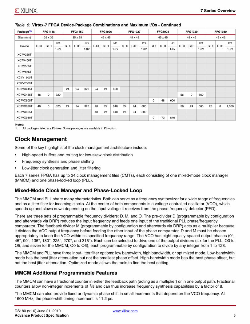
Table 8: Virtex-7 FPGA Device-Package Combinations and Maximum I/Os - Continued
Package(1) FFG1158 FFG1159 FFG1926 FFG1927 FFG1928 FFG1929 FFG1930
Size (mm) 35 x 35 35 x 35 45 x 45 45 x 45 45 x 45 45 x 45 45 x 45
Device GTX GTHI/O
GTX GTHI/O
GTX GTHI/O
GTX GTHI/O
GTX GTHI/O
GTX GTHI/O
GTX GTHI/O
1.8V 1.8V 1.8V 1.8V 1.8V 1.8V 1.8V
XC7V285T
XC7V450T
XC7V585T
XC7V855T
XC7V1500T
XC7V2000T
XC7VX415T 24 24 320 24 24 600
XC7VX485T 48 0 320 56 0 560
XC7VX605T 0 48 600
XC7VX690T 48 0 320 24 24 320 48 24 640 24 24 880 56 24 560 28 0 1,000
XC7VX895T 48 24 640 24 24 880
XC7VX910T 0 72 640
Notes: 1. All packages listed are Pb-free. Some packages are available in Pb option.
7 Series Overview
DS180 (v1.0) June 21, 2010 www.xilinx.comAdvance Product Specification 6
Clock Distribution
Each 7 series FPGA provides six different types of clock lines (BUFG, BUFR, BUFIO, BUFH, BUFMR, and the high-performance clock) to address the different clocking requirements of high fanout, short propagation delay, and extremely low skew.
Global Clock Lines
In each 7 series FPGA, 32 global clock lines have the highest fanout and can reach every flip-flop clock, clock enable, and set/reset, as well as many logic inputs. There are 12 global clock lines within any clock region driven by the horizontal clock buffers (BUFH). Each BUFH can be independently enabled/disabled, allowing for clocks to be turned off within a region, thereby offering fine-grain control over which clock regions consume power. Global clock lines can be driven by global clock buffers, which can also perform glitchless clock multiplexing and clock enable functions. Global clocks are often driven from the CMT, which can completely eliminate the basic clock distribution delay.
Regional Clocks
Regional clocks can drive all clock destinations in their region. A region is defined as any area that is 50 I/O and 50 CLB high and half the chip wide. 7 series FPGAs have between eight and twenty-four regions. There are four regional clock tracks in every region. Each regional clock buffer can be driven from either of four clock-capable input pins, and its frequency can optionally be divided by any integer from 1 to 8.
I/O Clocks
I/O clocks are especially fast and serve only I/O logic and serializer/deserializer (SerDes) circuits, as described in the I/O Logic section. The 7 series devices have a direct connection from the MMCM to the I/O for low-jitter, high-performance interfaces.
Block RAMSome of the key features of the block RAM include:
• Dual-port 36 Kb block RAM with port widths of up to 72
• Programmable FIFO logic
• Built-in optional error correction circuitry
Every 7 series FPGA has between 20 and 1,800 dual-port block RAMs, each storing 36 Kb. Each block RAM has two completely independent ports that share nothing but the stored data.
Synchronous Operation
Each memory access, read or write, is controlled by the clock. All inputs, data, address, clock enables, and write enables are registered. Nothing happens without a clock. The input address is always clocked, retaining data until the next operation. An optional output data pipeline register allows higher clock rates at the cost of an extra cycle of latency.
During a write operation, the data output can reflect either the previously stored data, the newly written data, or can remain unchanged.
7 Series Overview
DS180 (v1.0) June 21, 2010 www.xilinx.comAdvance Product Specification 7
Programmable Data Width
Each port can be configured as 32K × 1, 16K × 2, 8K × 4, 4K × 9 (or 8), 2K × 18 (or 16), 1K × 36 (or 32), or 512 × 72 (or 64). The two ports can have different aspect ratios without any constraints.
Each block RAM can be divided into two completely independent 18 Kb block RAMs that can each be configured to any aspect ratio from 16K × 1 to 512 × 36. Everything described previously for the full 36 Kb block RAM also applies to each of the smaller 18 Kb block RAMs.
Only in simple dual-port (SDP) mode can data widths of greater than 18 bits (18 Kb RAM) or 36 bits (36 Kb RAM) be accessed. In this mode, one port is dedicated to read operation, the other to write operation. In SDP mode, one side (read or write) can be variable, while the other is fixed to 32/36 or 64/72.
Both sides of the dual-port 36 Kb RAM can be of variable width.
Two adjacent 36 Kb block RAMs can be configured as one cascaded 64K × 1 dual-port RAM without any additional logic.
Error Detection and Correction
Each 64-bit-wide block RAM can generate, store, and utilize eight additional Hamming code bits and perform single-bit error correction and double-bit error detection (ECC) during the read process. The ECC logic can also be used when writing to or reading from external 64- to 72-bit-wide memories.
FIFO ControllerThe built-in FIFO controller for single-clock (synchronous) or dual-clock (asynchronous or multirate) operation increments the internal addresses and provides four handshaking flags: full, empty, almost full, and almost empty. The almost full and almost empty flags are freely programmable. Similar to the block RAM, the FIFO width and depth are programmable, but the write and read ports always have identical width.
First word fall-through mode presents the first-written word on the data output even before the first read operation. After the first word has been read, there is no difference between this mode and the standard mode.
Digital Signal Processing — DSP SliceSome highlights of the DSP functionality include:
• 25 × 18 two's complement multiplier/accumulator high-resolution (48 bit) signal processor
• Power saving pre-adder to optimize symmetrical filter applications
• Advanced features: optional pipelining, optional ALU, and dedicated buses for cascading
DSP applications use many binary multipliers and accumulators, best implemented in dedicated DSP slices. All 7 series FPGAs have many dedicated, full custom, low-power DSP slices, combining high speed with small size while retaining system design flexibility.
Each DSP slice fundamentally consists of a dedicated 25 × 18 bit two's complement multiplier and a 48-bit accumulator, both capable of operating at 600 MHz. The multiplier can be dynamically bypassed, and two 48-bit inputs can feed a single-instruction-multiple-data (SIMD) arithmetic unit (dual 24-bit add/subtract/accumulate or quad 12-bit add/subtract/accumulate), or a logic unit that can generate any one of ten different logic functions of the two operands.
The DSP includes an additional pre-adder, typically used in symmetrical filters. This new pre-adder improves performance in densely packed designs and reduces the DSP slice count by up to 50%.
The DSP slice provides extensive pipelining and extension capabilities that enhance the speed and efficiency of many applications beyond digital signal processing, such as wide dynamic bus shifters, memory address generators, wide bus multiplexers, and memory-mapped I/O register files. The accumulator can also be used as a synchronous up/down counter. The multiplier can perform logic functions (AND, OR) and barrel shifting.
7 Series Overview
DS180 (v1.0) June 21, 2010 www.xilinx.comAdvance Product Specification 8
Input/OutputSome highlights of the input/output functionality include:
• High-performance SelectIO technology with support for 2,133 Mb/s DDR3
• High-frequency decoupling capacitors within the package for enhanced signal integrity
• Digitally Controlled Impedance that can be 3-stated for lowest power, high-speed I/O operation
The number of I/O pins varies depending on device and package size. Each I/O is configurable and can comply with a large number of I/O standards. With the exception of the supply pins and a few dedicated configuration pins, all other package pins have the same I/O capabilities, constrained only by certain banking rules.
All I/O pins are organized in banks, with 50 pins per bank. Each bank has one common VCCO output supply, which also powers certain input buffers. Some single-ended input buffers require an internally generated or an externally applied reference voltage (VREF). There are two VREF pins per bank (except configuration bank 0). A single bank can have only one VREF voltage value.
Xilinx 7 series FPGAs use a variety of package types to suit the needs of the user, including small form factor wire-bond packages for lowest cost; conventional, high performance flip-chip packages; and lidless flip-chip packages that balance smaller form factor with high performance. In the flip-chip packages, the silicon device is attached to the package substrate using a high-performance flip-chip process. Controlled ESR discrete decoupling capacitors are mounted on the package substrate to optimize signal integrity under simultaneous switching of outputs (SSO) conditions.
I/O Electrical Characteristics
Single-ended outputs use a conventional CMOS push/pull output structure driving High towards VCCO or Low towards ground, and can be put into a high-Z state. The system designer can specify the slew rate and the output strength. The input is always active but is usually ignored while the output is active. Each pin can optionally have a weak pull-up or a weak pull-down resistor.
Any signal pin pair can be configured as a differential input pair or output pair. Differential input pin pairs can optionally be terminated with a 100Ω internal resistor. All 7 series devices support differential standards beyond LVDS: HT, RSDS, BLVDS, differential SSTL, and differential HSTL.
Each of the I/Os supports memory I/O standards, such as single-ended and differential HSTL as well as single-ended SSTL and differential SSTL. The SSTL I/O standard can support data rates of up to 2.133 Gb/s for DDR3 interfacing applications.
3-State Digitally Controlled Impedance and Low Power I/O Features
The 3-state Digitally Controlled Impedance (T_DCI) can control the output drive impedance (series termination) or can provide parallel termination of an input signal to VCCO or split (Thevenin) termination to VCCO/2. This allows users to eliminate off-chip termination for signals using T_DCI. In addition to board space savings, the termination will automatically turn off when in output mode or when 3-stated, saving considerable power compared to off-chip termination. The I/Os also have low power modes for IBUF and IDELAY to provide further power savings, especially when used to implement memory interfaces.
I/O Logic
Input and Output Delay
This section describes the available logic resources connected to the I/O interfaces. All inputs and outputs can be configured as either combinatorial or registered. Double data rate (DDR) is supported by all inputs and outputs. Any input and some outputs can be individually delayed by up to 32 increments of 78 ps or 52 ps each. Such delays are implemented as IDELAY and ODELAY. The number of delay steps can be set by configuration and can also be incremented or decremented while in use.
7 Series Overview
DS180 (v1.0) June 21, 2010 www.xilinx.comAdvance Product Specification 9
ISERDES and OSERDES
Many applications combine high-speed, bit-serial I/O with slower parallel operation inside the device. This requires a serializer and deserializer (SerDes) inside the I/O structure. Each I/O pin posseses an 8-bit IOSERDES (ISERDES and OSERDES) capable of performing serial-to-parallel or parallel-to-serial conversions with programmable widths of 2, 3, 4, 5, 6, 7, or 8 bits. By cascading two IOSERDES from two adjacent pins (default from differential I/O), wider width conversions of 10 and 14 bits can also be supported. The ISERDES has a special oversampling mode capable of asynchronous data recovery for applications like a 1.25 Gb/s LVDS I/O-based SGMII interface.
Low-Power Gigabit TransceiversSome highlights of the Low-Power Gigabit Transceivers include:
• High-performance GTX transceivers capable of up to 3.75 Gb/s, 10.3125 Gb/s or 13.1 Gb/s line rates depending on the family
• Low-power mode optimized for chip-to-chip interfaces
• Advanced Transmit pre and post emphasis, and receiver linear (CTLE) and decision feedback equalization (DFE), including adaptive equalization for additional margin.
Ultra-fast serial data transmission to optical modules, between ICs on the same PCB, over the backplane, or over longer distances is becoming increasingly popular and important to enable customer line cards to scale to 100 Gb/s and onwards to 400 Gb/s. It requires specialized dedicated on-chip circuitry and differential I/O capable of coping with the signal integrity issues at these high data rates.
All 7 series devices have from 4 to 72 gigabit transceiver circuits. Each serial transceiver is a combined transmitter and receiver. All 7 series serial transceivers share the same hybrid architecture, combining ring oscillators and LC tank oscillators to allow the ideal blend of flexibility and performance while enabling IP portability across the family members. The different 7 series family members offer different top-end data rates. The GTP operates up to 3.75 Gb/s, the GTX operates up to 10.3125 Gb/s, and the GTH operates up to 13.1 Gb/s. Lower data rates can be achieved using FPGA logic-based oversampling. The serial transmitter and receiver are independent circuits that use an advanced PLL architecture to multiply the reference frequency input by certain programmable numbers between 4 and 25 to become the bit-serial data clock. Each transceiver has a large number of user-definable features and parameters. All of these can be defined during device configuration, and many can also be modified during operation.
Transmitter
The transmitter is fundamentally a parallel-to-serial converter with a conversion ratio of 16, 20, 32, 40, 64, or 80 to allow the designer to trade-off datapath width for timing margin in high-performance designs. These transmitter outputs drive the PC board with a single-channel differential current-mode logic (CML) output signal. TXOUTCLK is the appropriately divided serial data clock and can be used directly to register the parallel data coming from the internal logic. The incoming parallel data is fed through an optional FIFO and has additional hardware support for the 8B/10B, 64B/66B, or 64B/67B encoding schemes to provide a sufficient number of transitions. The bit-serial output signal drives two package pins with complementary CML signals. This output signal pair has programmable signal swing as well as programmable pre- and post-emphasis to compensate for PC board losses and other interconnect characteristics. For shorter channels, the swing can be reduced to reduce power consumption.
Receiver
The receiver is fundamentally a serial-to-parallel converter, changing the incoming bit-serial differential signal into a parallel stream of words, each 16, 20, 32, 40, 64, or 80 bits wide to allow the FPGA designer to trade-off internal datapath width versus logic timing margin. The receiver takes the incoming differential data stream, feeds it through programmable linear and decision feedback equalizers (to compensate for PC board and other interconnect characteristics), and uses the reference clock input to initiate clock recognition. There is no need for a separate clock line. The data pattern uses non-return-to-zero (NRZ) encoding and optionally guarantees sufficient data transitions by using the selected encoding scheme. Parallel data is then transferred into the FPGA logic using the RXUSRCLK clock. The serial-to-parallel conversion ratio for serial transceivers can be 16, 20, 32, 40, 64, or 80. For short channels, the transceivers offers a special low power mode (LPM) to reduce power consumption by approximately 30%.
7 Series Overview
DS180 (v1.0) June 21, 2010 www.xilinx.comAdvance Product Specification 10
Out-of-Band Signaling
The GTX transceivers provide out-of-band (OOB) signaling, often used to send low-speed signals from the transmitter to the receiver while high-speed serial data transmission is not active. This is typically done when the link is in a powered-down state or has not yet been initialized. This benefits PCI Express and SATA/SAS applications.
Integrated Interface Blocks for PCI Express Designs Highlights of the integrated blocks for PCI Express include:
• Compliant to the PCI Express Base Specification 2.1 with Endpoint and Root Port capability
• Up to x8 Gen1 (2.5 Gb/s) and Gen2 (5 Gb/s) support with integrated transceivers
• Advanced error reporting and ECRC
• Multiple-function and single root I/O virtualization (SR-IOV) support enabled through soft-logic wrappers
All 7 series devices with transceivers include at least one integrated block for PCI Express technology that can be configured as an Endpoint or Root Port, compliant to the PCI Express Base Specification Revision 2.1. The Root Port can be used to build the basis for a compatible Root Complex, to allow custom FPGA-to-FPGA communication via the PCI Express protocol, and to attach ASSP Endpoint devices, such as Fibre Channel HBAs, to the FPGA.
This block is highly configurable to system design requirements and can operate 1, 2, 4, or 8 lanes at the 2.5 Gb/s and 5.0 Gb/s data rates. For high-performance applications, advanced buffering techniques of the block offer a flexible maximum payload size of up to 1,024 bytes. The integrated block interfaces to the integrated high-speed transceivers for serial connectivity and to block RAMs for data buffering. Combined, these elements implement the Physical Layer, Data Link Layer, and Transaction Layer of the PCI Express protocol.
Xilinx provides a light-weight, configurable, easy-to-use LogiCORE™ IP wrapper that ties the various building blocks (the integrated block for PCI Express, the transceivers, block RAM, and clocking resources) into an Endpoint or Root Port solution. The system designer has control over many configurable parameters: lane width, maximum payload size, FPGA logic interface speeds, reference clock frequency, and base address register decoding and filtering.
Xilinx offers three wrappers for the integrated block: 1) AXI-ST Basic, 2) AXI-ST Enhanced and 3) AXI-MM. Note that legacy TRN/Local Link is not available in 7 series devices for the integrated block for PCI Express. AXI-ST Basic is designed for existing customers of the integrated block and enables easy migration to AXI from TRN. AXI-ST Enhanced is targeted for new designs and new users and contains additional logic that enhances ease-of-use and provides faster time to market. AXI-MM is designed for Xilinx Platform Studio/EDK design flow and MicroBlaze™ processor based designs.
More information and documentation on solutions for PCI Express designs can be found at: http://www.xilinx.com/technology/protocols/pciexpress.htm.
ConfigurationThere are many advanced configuration features, including:
• High-speed SPI and BPI (parallel NOR) configuration
• Built-in MultiBoot and safe-update capability
• 256-bit AES encryption with HMAC authentication
• Built-in SEU detection and correction
• Partial reconfiguration
Xilinx 7 series FPGAs store their customized configuration in SRAM-type internal latches. The number of configuration bits is between 5 Mb and 431 Mb (0.6 MB to 54 MB), depending on device size but independent of the specific user-design implementation, unless compression mode is used. The configuration storage is volatile and must be reloaded whenever the FPGA is powered up. This storage can also be reloaded at any time by pulling the PROGRAM_B pin Low. Several methods and data formats for loading configuration are available, determined by the three mode pins.
The SPI interface (x1, x2, and x4 modes) and the BPI interface (parallel-NOR x8 and x16) are two common methods used for configuring the FPGA. Users can directly connect an SPI or BPI flash to the FPGA, and the FPGA's internal configuration
7 Series Overview
DS180 (v1.0) June 21, 2010 www.xilinx.comAdvance Product Specification 11
logic reads the bitstream out of the flash and configures itself. The FPGA automatically detects the bus width on the fly, eliminating the need for any external controls or switches. Bus widths supported are x1, x2, and x4 for SPI, and x8 and x16 for BPI. The larger bus widths increase configuration speed and reduce the amount of time it takes for the FPGA to start up after power-on.
In master mode, the FPGA can drive the configuration clock from an internally generated clock, or for higher speed configuration, the FPGA can use an external configuration clock source. This allows high-speed configuration with the ease of use characteristic of master mode. Slave modes up to 32 bits wide are also supported by the FPGA that are especially useful for processor-driven configuration.
The FPGA has the ability to reconfigure itself with a different image using SPI or BPI flash, eliminating the need for an external controller. The FPGA can reload its original design in case there are any errors in the data transmission, ensuring an operational FPGA at the end of the process. This is especially useful for updates to a design after the end product has been shipped. Customers can ship their products with an early version of the design, thus getting their products to market faster. This feature allows customers to keep their end users current with the most up-to-date designs while the product is already in the field.
The dynamic reconfiguration port (DRP) gives the system designer easy access to the configuration and status registers of the MMCM, PLL, XADC, transceivers, and integrated block for PCI Express. The DRP behaves like a set of memory-mapped registers, accessing and modifying block-specific configuration bits as well as status and control registers.
Encryption, Readback, and Partial Reconfiguration
In all Artix-7 devices over 100K logic cells, all Kintex-7 devices, and all Virtex-7 devices, the FPGA bitstream, which contains sensitive customer IP, can be protected with 256-bit AES encryption and HMAC authentication to prevent unauthorized copying of the design. The FPGA performs decryption on the fly during configuration using an internally stored 256-bit key. This key can reside in battery-backed RAM or in nonvolatile eFUSE bits.
Most configuration data can be read back without affecting the system's operation. Typically, configuration is an all-or-nothing operation, but Xilinx 7 series FPGAs support partial reconfiguration. This is an extremely powerful and flexible feature that allows the user to change portions of the FPGA while other portions remain static. Users can time-slice these portions to fit more IP into smaller devices, saving cost and power. Where applicable in certain designs, partial reconfiguration can greatly improve the versatility of the FPGA.
XADC (Analog-to-Digital Converter)Highlights of the XADC architecture include:
• Dual 12-bit 1 MSPS analog-to-digital converters (ADCs)
• On-chip temperature and power supply sensors
• Easy JTAG access to ADC measurements
• Full support for legacy SYSMON designs
Every 7 series FPGA family member with a logic density greater than 100,000 logic cells contains a general-purpose analog interface called the XADC, which contains two 12-bit 1 MSPS ADCs, on-chip sensors, and external analog input channels. The XADC offers enhanced functionality over the System Monitor found in previous generations of Virtex FPGAs.
These 12-bit ADCs support sample rates of up to one million samples per second and can simultaneously sample two external-input analog channels. (7 series FPGAs support up to 17 external analog input channels.) The ADCs support a diverse range of applications that need to process analog signals with bandwidths of less than 500 KHz.
The XADC optionally uses an on-chip reference circuit, thereby eliminating the need for any external active components for basic on-chip monitoring of temperature and power supply rails. To achieve the full 12-bit performance of the ADCs, an external 1.25V reference IC is recommended. The on-chip temperature and power supplies are monitored with a measurement accuracy of ±4°C and ±1%, respectively, using either reference source.
By default, the XADC continuously digitizes the output of all on-chip sensors. The most recent measurement results (together with maximum and minimum readings) are stored in dedicated registers for access at any time via on-chip or external JTAG interfaces. User-defined alarm thresholds can automatically indicate over-temperature events and
7 Series Overview
DS180 (v1.0) June 21, 2010 www.xilinx.comAdvance Product Specification 12
unacceptable power supply variation. A user-specified limit (for example, 100°C) can be used to initiate an automatic power-down.
7 Series FPGA Ordering InformationThis document is a pre-release document, provided ahead of silicon ordering availability. Therefore, Xilinx 7 series FPGA ordering information is not yet available. Please contact your Xilinx sales representative for more information on 7 series Early Access Programs.
Revision HistoryThe following table shows the revision history for this document:
Notice of DisclaimerTHE XILINX HARDWARE FPGA AND CPLD DEVICES REFERRED TO HEREIN (“PRODUCTS”) ARE SUBJECT TO THE TERMS ANDCONDITIONS OF THE XILINX LIMITED WARRANTY WHICH CAN BE VIEWED AT http://www.xilinx.com/warranty.htm. THIS LIMITEDWARRANTY DOES NOT EXTEND TO ANY USE OF PRODUCTS IN AN APPLICATION OR ENVIRONMENT THAT IS NOT WITHIN THESPECIFICATIONS STATED IN THE XILINX DATA SHEET. ALL SPECIFICATIONS ARE SUBJECT TO CHANGE WITHOUT NOTICE.PRODUCTS ARE NOT DESIGNED OR INTENDED TO BE FAIL-SAFE OR FOR USE IN ANY APPLICATION REQUIRING FAIL-SAFEPERFORMANCE, SUCH AS LIFE-SUPPORT OR SAFETY DEVICES OR SYSTEMS, OR ANY OTHER APPLICATION THAT INVOKESTHE POTENTIAL RISKS OF DEATH, PERSONAL INJURY, OR PROPERTY OR ENVIRONMENTAL DAMAGE (“CRITICALAPPLICATIONS”). USE OF PRODUCTS IN CRITICAL APPLICATIONS IS AT THE SOLE RISK OF CUSTOMER, SUBJECT TOAPPLICABLE LAWS AND REGULATIONS.
Date Version Description of Revisions
06/21/10 1.0 Initial Xilinx release.