Embed Size (px)
Citation preview

73M2901CE V.22bis Single Chip Modem
Simplifying System Integration™ DATA SHEET
DS_2901CE_031 January 2010
Rev. 3.4 © 2010 Teridian Semiconductor Corporation 1
DESCRIPTION
The 73M2901CE low speed modem integrates a data pump, controller, and analog front end in a 3.3 V device with a powerful "AT" command host interface. The modem reduces external component count/cost by incorporating many features like parallel phone detect, Line-In-Use and Ring detection in software without requiring additional components. The device is a "one chip fits all” solution for applications including set-top boxes, point-of-sale terminals, automatic teller machines, utility meters, vending machines and smart card readers. Another distinctive feature of this device is pin compatibility with Teridian’s flagship embedded hard modems, the 73M2901CL, and the 73M1903 soft modem AFE. This offers customers a cost effective method to design for both hard or soft modem solutions in the same system as a risk-free cost reduction path. Complete support, modem reference designs and error correction software are part of the solution offered by Teridian. Our in-house application engineering team is here to help meet your international certification needs.
FEATURES
• True one chip solution for embedded systems • As low as 9.5 mA operating with standby and
power down mode available • Power supply operation from 3.6 V to 2.7 V • Data modes and speeds:
V.22bis – 2400 bps V.22/Bell212 – 1200 bps V.21/Bell103 – 300 bps V.23 – 1200/75 bps (with PAVI turnaround) Bell202 – 1200 bps Bell202/V23 1200 bps FDX 4-wire operation
• V.22/Bell 212A/V.22bis synchronous modes • International Call Progress support:
FCC part 68, CTR21, JATE, etc. • DTMF generation and detection • Worldwide Caller ID capability
U.S. Type I and II support • EIA 777A compliant • SIA-2000 compliant • SMS messaging support • On chip hybrid driver • Blacklisting capability • Line-In-Use and Parallel Pick-Up (911) detection
with voltage or low cost energy detection method • Incoming ring energy detection through CID
path; no optocoupler circuitry required • Manufacturing Self Test capability • Backward compatible with 73M2901CL • Packaging: 32 lead QFN, 32-pin TQFP

73M2901CE Data Sheet DS_2901CE_031
2 Rev. 3.4
Table of Contents 1 Hardware Description .................................................................................................................... 4
1.1 Power Supply ....................................................................................................................... 4 1.2 Low Power Mode .................................................................................................................. 4 1.3 Analog Line / Hybrid Interface ............................................................................................... 4 1.4 Interrupt Pins ........................................................................................................................ 4 1.5 Crystal Oscillator................................................................................................................... 5
1.5.1 Specifying a Crystal ..................................................................................................... 5 1.6 Reset .................................................................................................................................... 5 1.7 Asynchronous and Synchronous Serial Data Interface .......................................................... 5
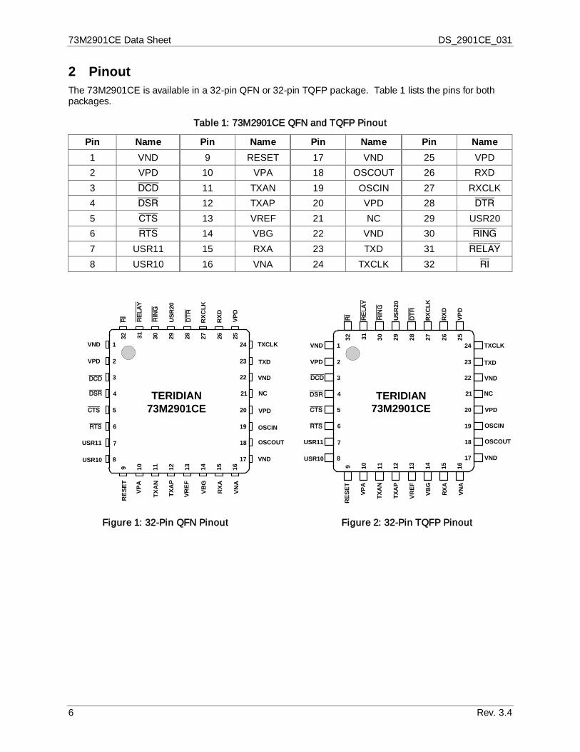
2 Pinout ............................................................................................................................................. 6 3 Pin Descriptions ............................................................................................................................ 7
3.1 Power Pins ........................................................................................................................... 7 3.2 Analog Interface Pins ............................................................................................................ 7 3.3 Digital Interface Pins ............................................................................................................. 7 3.4 External Interrupt Pins .......................................................................................................... 8 3.5 Oscillator Pins ....................................................................................................................... 8
4 Electrical Specifications ................................................................................................................ 9 4.1 Absolute Maximum Ratings................................................................................................... 9 4.2 Recommended Operating Conditions .................................................................................... 9 4.3 Receiver ............................................................................................................................... 9 4.4 Transmitter ......................................................................................................................... 10 4.5 Maximum Transmit Level .................................................................................................... 10 4.6 DC Characteristics, Vcc = 3.3 V .......................................................................................... 11
4.6.1 DC Supply Current, VDD = 2.7 V (Battery EOL) ......................................................... 11 4.6.2 DC Supply Current , VDD = 3.0 V .............................................................................. 11 4.6.3 DC Supply Current VDD = 3.3 V ................................................................................ 12 4.6.4 DC Supply Current VDD = 3.6 V ................................................................................ 12
5 Firmware Description .................................................................................................................. 13 5.1 Firmware Overview ............................................................................................................. 13 5.2 Firmware Features .............................................................................................................. 13
6 Design Considerations ................................................................................................................ 14 6.1 Layout Considerations ........................................................................................................ 14 6.2 73M2901CE Design Compatibility ....................................................................................... 15 6.3 Telephone Line Interface .................................................................................................... 15 6.4 Functional Considerations ................................................................................................... 16
6.4.1 SMS and V.23 Half Duplex ........................................................................................ 16 6.4.2 Leased Line Mode ..................................................................................................... 16 6.4.3 73M2901CE Energy Ring Detection .......................................................................... 17 6.4.4 Caller ID Mode Changes ........................................................................................... 18 6.4.5 Selectable Answer Tone Frequency Detection ........................................................... 18 6.4.6 73M2901CE S99 Country Code Support ................................................................... 18
7 Reference Designs ...................................................................................................................... 21 7.1 Low Cost Design Using DSP Ring and Status Monitoring .................................................... 21 7.2 Reference Design Using Traditional Hardware Line Monitoring ........................................... 22
8 Modem Performance Characteristics ......................................................................................... 23 8.1 BER versus SNR ................................................................................................................ 23 8.2 BER versus Receive Level .................................................................................................. 23
9 Package Mechanical Drawing ..................................................................................................... 24 9.1 32-Pin QFN ........................................................................................................................ 24 9.2 32-Pin TQFP....................................................................................................................... 25
10 Ordering Information ................................................................................................................... 26 11 Related Documentation ............................................................................................................... 26 12 Contact Information ..................................................................................................................... 26 Revision History .................................................................................................................................. 27

DS_2901CE_031 73M2901CE Data Sheet
Rev. 3.4 3
Figures Figure 1: 32-Pin QFN Pinout ................................................................................................................ 6Figure 2: 32-Pin TQFP Pinout .................................................................................................................. 6 Figure 3: Low Cost Design Using DSP Ring and Status Monitoring ........................................................ 21Figure 4: 73M2901CE Worldwide Demo Board: Daughter Board Schematic .......................................... 22Figure 5: BER versus SNR .................................................................................................................... 23Figure 6: BER versus Receive Level ...................................................................................................... 23 Figure 7: 32-Pin QFN Drawing ............................................................................................................... 24Figure 8: 32-Pin TQFP Drawing ............................................................................................................. 25 Tables Table 1: 73M2901CE QFN and TQFP Pinout ........................................................................................... 6Table 2: Leased Line Initialization Commands ....................................................................................... 16Table 3: Approximate Thresholds for Energy Ring Detection .................................................................. 17Table 4: 73M2901CE Order Numbers and Packaging Marks .................................................................. 26

73M2901CE Data Sheet DS_2901CE_031
4 Rev. 3.4
1 Hardware Description The 73M2901CE is designed to operate from a +3.6 to +2.7 volt supply with low power consumption (~30 mW @ 3.0 volts). The modem supports automatic standby idle mode. The modem will also accept a request to power down from the DTE via hardware control. No additional major components are required to complete the modem core logic. The modem provides direct firmware LED support via the port pins (pins 3, 4, 5, 6, 31, and 32). The 73M2901 CE includes the following hardware features:
• Fully self-contained. “AT” Command interpreter and data pump. • User pins available. • Synchronous serial data I/O available. • Asynchronous serial port. • On-chip hybrid and line driver. • Autobaud capability from 300 bps to 9600 bps. • Reduced external hardware support required with energy incoming ring detection. 1.1 Power Supply Power is supplied to the 73M2901CE by the VPD and VPA pins. The 73M2901CE is designed for a single +3.6 to +2.7 volt supply and for low power consumption (~30mW @ 3.0 volts). Ground is supplied to the 73M2901CE by the VND and VNA pins. The 73M2901CE has been designed with separated analog and digital supplies to insure the best performance of the part by using separately filtered power supplies. It is recommended that separate locally bypassed traces be used to apply power to the analog supply VPA and the digital supply VPD. 1.2 Low Power Mode The Teridian 73M2901CE supports a low power standby mode. If the low power standby option is enabled, the 73M2901CE will go into a power saving mode when idle. While in this mode, the oscillator will be running and clocks will be supplied to the UART, timers and interrupt blocks, but no clocks will be supplied to the CPU. Instruction processing and activity on the internal busses is halted. Normal operation is resumed when an interruption such as assertion of DTR or RING occurs, a character is sent to the 73M2901CE TXD input, or a reset occurs. 1.3 Analog Line / Hybrid Interface The 73M2901CE provides a differential analog output (TXAP and TXAN) and a single-ended analog input (RXA) with internal A/D and D/A converters. A driver is provided for an internal hybrid function. The internal hybrid driver is capable of driving an external load matching impedance and a line-coupling transformer. The internal hybrid/line driver senses the load and adapts itself to its requirements. The 73M2901CE provides firmware control for a hook relay driver (RELAY) as well as interrupt support for a ring detect opto-coupler (RING). 1.4 Interrupt Pins The external interrupt sources, DTR and RING, come from dedicated input pins of the same name. DTR informs the 73M2901CE that the host has requested the 73M2901CE to perform a specific function. The function of DTR can be changed by “AT” commands (described in the 73M2901CE AT Command User Guide).

DS_2901CE_031 73M2901CE Data Sheet
Rev. 3.4 5
RING is used to inform the 73M2901CE that the external DAA circuitry or ring energy detector has detected a ring signal. It will go active when each “RING” message is sent on RXD. In addition, sending any character on the TXD line also generates an internal interrupt. 1.5 Crystal Oscillator The Teridian 73M2901CE single chip modem can use an external 11.0592 MHz reference clock or can generate a clock using only a crystal and two capacitors. If an external clock is used, it should be applied to the OSCIN pin. 1.5.1 Specifying a Crystal The manufacturer of a crystal resonator verifies its frequency of oscillation in a test set-up, but to ensure that the same frequency is obtained in the application, the circuit conditions must be the same. The Teridian 73M2901CE modem requires a parallel mode (anti-resonant) crystal, the important specifications of which are as follows: Mode: Parallel (anti-resonant) Frequency: 11.0592 MHz Frequency tolerance: ±50 ppm at initial temperature Temperature drift: An additional ±50 ppm over full range Load capacitance: 18 pF to 22 pF ESR: 75 Ω max Drive level: Less than 1 mW The peak voltage level of the oscillator should be checked to assure it will not violate the maximum voltage levels allowed on the oscillator pins. A resistor in series with the crystal can be used, if necessary, to reduce the oscillator’s peak voltage levels. Crystals with low ESRs may oscillate at higher than specified voltage levels. 1.6 Reset A reset is accomplished by holding the RESET pin high. To ensure a proper power-on reset, the reset pin must be held high for a minimum of 3 µs. At power on, the voltage at VPD, VPA, and RESET must come up at the same time for a proper reset. The signals DCD, CTS and DSR will be held inactive for 25 ms, acknowledging the reset operation, within a 250 ms time window after the reset-triggering event. The 73M2901CE is ready for operation after the 250 ms window and/or after the signals DCD, CTS and DSR become active. 1.7 Asynchronous and Synchronous Serial Data Interface The serial data interface consists of the TXD and RXD data paths (LSB shifted in and out first) and the TXCLK and RXCLK serial synchronous clock outputs associated with the data pins; CTS/RTS flow control; DCD, DSR and DTR. In asynchronous mode, the data is passed at the bit rate (tolerance is +1%, -2.5%).
73M2901CE Data Sheet DS_2901CE_031
6 Rev. 3.4
2 Pinout The 73M2901CE is available in a 32-pin QFN or 32-pin TQFP package. Table 1 lists the pins for both packages.
Table 1: 73M2901CE QFN and TQFP Pinout
Pin Name Pin Name Pin Name Pin Name 1 VND 9 RESET 17 VND 25 VPD 2 VPD 10 VPA 18 OSCOUT 26 RXD 3 DCD 11 TXAN 19 OSCIN 27 RXCLK 4 DSR 12 TXAP 20 VPD 28 DTR
5 CTS 13 VREF 21 NC 29 USR20 6 RTS 14 VBG 22 VND 30 RING
7 USR11 15 RXA 23 TXD 31 RELAY
8 USR10 16 VNA 24 TXCLK 32 RI
6
7
8
9
5
4
3
2
1
17
18
19
20
24
23
22
21
10 11 12 13 14 15 16
32 31 30 29 28 27 26 25
VND
VPD
DCD
DSR
CTS
RTS
USR11
USR10
TXCLK
TXD
VND
NC
VPD
OSCIN
OSCOUT
VND
RES
ET
VPA
TXA
N
TXA
P
VREF
VBG
RXA
VNA
TERIDIAN 73M2901CE
VPD
RI
RE
LAY
RIN
G
USR
20
DT
R
RXC
LK
RXD
Figure 1: 32-Pin QFN Pinout Figure 2: 32-Pin TQFP Pinout
6
7
8
9
5
4
3
2
1
17
18
19
20
24
23
22
21
10 11 12 13 14 15 16
32 31 30 29 28 27 26 25
VND
VPD
DCD
DSR
CTS
RTS
USR11
USR10
TXCLK
TXD
VND
NC
VPD
OSCIN
OSCOUT
VND
RES
ET
VPA
TXA
N
TXA
P
VREF
VBG
RXA
VNA
TERIDIAN73M2901CE
VPD
RI
RE
LAY
RIN
G
USR
20
DT
R
RXC
LK
RXD

DS_2901CE_031 73M2901CE Data Sheet
Rev. 3.4 7
3 Pin Descriptions 3.1 Power Pins Pin Name Pin Number Type Description VPA 10 I Positive analog voltage (analog supply) VNA 16 I Negative analog voltage (analog ground) VPD 2, 20, 25 I Positive digital voltage (digital supply) VND 1, 17, 22 I Negative digital voltage (digital ground)
3.2 Analog Interface Pins Pin Name Pin Number Type Description RXA 15 I Receive analog input TXAN 11 O Transmit analog - output TXAP 12 O Transmit analog + output VBG 14 O Analog Band Gap voltage reference (0.1 µF to VNA). This pin
must not be connected to external circuitry other than the decoupling capacitor.
VREF 13 O Analog reference voltage (0.1 µF to VNA) 3.3 Digital Interface Pins Pin Name Pin Number Type Description RESET 9 I Reset RXCLK 27 O Receive data synchronous clock, valid on rising edge TXCLK 24 O Transmit data synchronous clock, valid on rising edge TXD 23 I Serial data input from DTE RXD 26 O Serial output to DTE USR10 8 I/O Programmable I/O port. This pin can optionally be used to
control an external switch for external Line In Use circuitry. USR11 7 I/O Programmable I/O port. This pin can optionally be used to
control an external switch for caller ID operation. RTS 6 I Request to send CTS 5 O Clear to send DSR 4 O Data set ready DCD 3 O Data carrier detect RI 32 O Ring indicator RELAY 31 O Relay driver output USR20 29 I/O Programmable I/O port

73M2901CE Data Sheet DS_2901CE_031
8 Rev. 3.4
3.4 External Interrupt Pins Pin Name Pin Number Type Description RING 30 I External interrupt – Line interface ring detection circuitry input DTR 28 I External interrupt – DTE DTR signal input
3.5 Oscillator Pins Pin Name Pin Number Type Description OSCIN 19 I Crystal input for internal oscillator, also input for external source OSCOUT 18 O Crystal oscillator output

DS_2901CE_031 73M2901CE Data Sheet
Rev. 3.4 9
4 Electrical Specifications 4.1 Absolute Maximum Ratings Parameter Rating Supply Voltage -0.5 V to +4.0 V Pin Input Voltage (except OSCIN) -0.5 V to + 6.0 V Pin Input Voltage (OSCIN) -0.5 V to VPD + 0.5 V Storage Temperature -55 ºC to 150 ºC
Absolute maximum ratings are stress ratings ONLY, functional operation of the device at these or any other conditions above those indicated in the recommended operation sections of this specification is not implied. Exposure to absolute maximum conditions for extended periods of time may affect reliability.
4.2 Recommended Operating Conditions Parameter Rating Supply Voltage 2.7 V to 3.6 V Oscillator Frequency 11.0592 MHz +/- 50 ppm Operating Temperature -40 ºC to 85 ºC
4.3 Receiver Parameter Conditions Min Nominal Max Units Carrier Detect On Tip and Ring -43 dBm01
Carrier Detect Off
Tip and Ring -48 dBm01 Carrier Detect Hysteresis Tip and Ring 2 dB Receive Level Tip and Ring -43 -9 dBm01 Idle Channel Noise 0.2 kHz to 4.0 kHz -70 -65 dB Input Impedance RXA 150 kΩ Receive Gain Boost S110 bit 5=1, CID mode 18.8 19.3 19.8 dB Max Input Level at RXA VREF=1.25 V 0.587 0.622 0.658 Vpk Total Harmonic Distortion (THD)
1kHz 450 mVpk on RXA THD=2nd and 3rd harmonic
-70 -50 dB
1 dBm0 refers to the Teridian recommended line interface (8 dB loss from transmit pins to the line and 5 dB loss from the line to the receiver pin). Results may vary depending on the selected DAA components. 0dBm=0.775 mVrms; dBm=10log(Vrms
2/(1mW)(600Ω))

73M2901CE Data Sheet DS_2901CE_031
10 Rev. 3.4
4.4 Transmitter Parameter Conditions Min Nominal Max Units ITU Guard tone power 550 Hz (relative to carrier) -5 -3.5 -2 dB
1800 Hz (relative to carrier) -8 -6.5 -5 dB Calling Tone 1300 Hz -11 -10 -9 dBm01
Answer Tone power
2225 Hz / 2100 Hz -11 -10 -9 dBm01 DTMF Transmit power High band tones -12 -11.5 -11 dBm01
Low band tones -13.7 -13.2 -12.7 dBm01 Gain adjust tolerance By step -0.3 0 0.3 dBm01 Total Harmonic Distortion (THD)
1 kHz sine wave at output (TXAP-TXAN) 1.5 Vpk (2.7 dBm) for VREF=1.25 V THD=2nd and 3rd harmonic
-50 dB
Intermod Distortion At output (TXAP-TXAN) 1 kHz, 1.2 kHz sine waves summed 2 Vpk for VREF=1.25 V
Each unwanted frequency component
-33 dBm
Sum of unwanted frequency components in pass band
-20 dB below
low tone Power supply rejection ratio
-30 dBm signal at VPA 300 Hz to 30 kHz measured TXAP to TXAN
30 dB
4.5 Maximum Transmit Level Parameter Conditions Min Nominal Max Units QAM VREF=1.25 V
VPA=3.3 V -9.6 dBm01
DPSK VREF=1.25 V VPA=3.3 V
-7.4 dBm01
FSK VREF=1.25 V VPA=3.3 V
-5.3 dBm01
DTMF (High Tone) VREF=1.25 V S13=$20, VPA=3.3 V S85=80
-8 -7 dBm01
DTMF (Low Tone) VREF=1.25V S13=$20, VPA=3.3V S85=80
-9.7 -8.7 dBm01
1 dBm0 refers to the Teridian recommended line interface (8 dB loss from transmit pins to the line and 5 dB loss from the line to the receiver pin). Results may vary depending on the selected DAA components. 0dBm=0.775 mVrms; dBm=10log(Vrms
2/(1mW)(600Ω)).

DS_2901CE_031 73M2901CE Data Sheet
Rev. 3.4 11
4.6 DC Characteristics, Vcc = 3.3 V (Vdd stands for VPD and VPA) Parameter Symbol Conditions Min Nom Max Unit Input low voltage (except OSCIN) VIL -0.5 0.8 V Input low voltage OSCIN VIL -0.5 0.2 Vdd V Input high voltage (except OSCIN) VIH 0.7 Vdd +5.5 V Input high voltage OSCIN VIH 0.7 Vdd Vdd+0.5 V Output low voltage (except OSCOUT) VOL IOL=4 mA 0.45 V Output low voltage OSCOUT VOLOSC IOL=3 mA 0.7 V Output high voltage (except OSCOUT) VOH IOH=-4 mA Vdd-0.45 V Output high voltage OSCOUT VOHOSC IOH=-3 mA Vdd-0.9 V Input leakage current (except OSCIN) IIH Vss<Vin<Vdd 1 µA
Input leakage current OSCIN IIH Vss<Vin<Vdd 1 30 µA Parameter Conditions Min Nom Max Unit VBG Vdd=3.3 V 1.19 1.25 1.31 V VREF Vdd=3.3 V 1.19 1.25 1.31 V TXAP to TXAN offset Vdd=3.3 V, steady state 50 mV
4.6.1 DC Supply Current, VDD = 2.7 V (Battery EOL)
Parameter Symbol Conditions Min Nom Max Unit Maximum power supply, normal operation
IDD1 30 pF/pin 9.5 10.5 mA
Maximum power supply, Idle mode
IDD2 30 pF/pin 900 1500 µA
Maximum power supply, Power Down mode
IDD3 30 pF/pin 10 µA
4.6.2 DC Supply Current , VDD = 3.0 V
Parameter Symbol Conditions Min Nom Max Unit Maximum power supply, normal operation
IDD1 30 pF/pin 10.6 11.9 mA
Maximum power supply, Idle mode
IDD2 30 pF/pin 1.1 1.7 mA
Maximum power supply, Power Down mode
IDD3 30 pF/pin 10 µA

73M2901CE Data Sheet DS_2901CE_031
12 Rev. 3.4
4.6.3 DC Supply Current VDD = 3.3 V
Parameter Symbol Conditions Min Nom Max Unit Maximum power supply, normal operation
IDD1 30 pF/pin 11.8 13.6 mA
Maximum power supply, Idle mode
IDD2 30 pF/pin 1.25 1.85 mA
Maximum power supply, Power Down mode
IDD3 30 pF/pin 10 µA
4.6.4 DC Supply Current VDD = 3.6 V
Parameter Symbol Conditions Min Nom Max Unit Maximum power supply, normal operation
IDD1 30 pF/pin 13.4 15.5 mA
Maximum power supply, Idle mode IDD2 30 pF/pin 1.4 2.0 mA Maximum power supply, Power Down mode
IDD3 30 pF/pin 10 µA

DS_2901CE_031 73M2901CE Data Sheet
Rev. 3.4 13
5 Firmware Description An “AT” command interpreter provides command and configuration of the 73M2901CE. This provides the user a uniform interface to control the modem in embedded applications. The signal processing is performed to provide data to the DAC and process data from the A/D converter. A MAC hardware coprocessor is provided for computation. To provide maximum flexibility, the system host processor can access the internal RAM and Control Register space in the modem. This will allow the OEM user to modify parameters such as filter response and transmit levels through the AT command set using proprietary commands. The host processor can also access the modem I/O port pins, providing extended I/O capability. Refer to the 73M2901CE AT Command User Guide for a complete description of the software. 5.1 Firmware Overview The modem always powers up in the idle (on hook) mode. “AT” commands are issued via the serial interface from the host. All modem configuration commands are received in this manner. The data modem firmware is contained in an internal ROM. The firmware will automatically enter a power saving idle mode if the modem is on hook and there are no incoming host commands. The modem automatically powers up upon receiving the next command. This power up sequence occurs without delay to the host. This function, while saving power, is transparent to the host processor and can be disabled by the host via an “AT” command. The host can also program the modem to power down via an external pin (DTR) or via a firmware command. 5.2 Firmware Features • “AT” command set • Supports data standards through V.22bis • Provides DAA control firmware (e.g. ring detect, hook control) • Multinational Call Progress support (FCC part 68, ITU CTR21, Japan JATE, etc.) • Caller ID capability • FSK demodulation (V.23, V.21, Bell 202 and Bell 103) • DTMF detection and decoding • Selectable number of rings and line reversal for CID data operation • On hook CID data operation • On hook Line-In-Use detection support (No line seizure will occur when a Line-In-Use condition is
detected) • Off hook Parallel Pick-Up detection support (Line seizure will be aborted as soon as a Parallel Pick-Up
condition is detected) • Off hook voltage change detection (requires external circuitry) • Receive energy change detection • Directly interfaces with standard V.24/EIA-232 bus drivers (3.3 V inverted level) serial interface using
the built in serial port and firmware control of port pins • Provides tone generation and detection including four imprecise and four precise call progress detect
filters with programmable frequency and detection threshold • Blacklisting capability • Long Space disconnect support • Inactivity timeout • Host access to program RAM provided • User programmable general purpose I/O

73M2901CE Data Sheet DS_2901CE_031
14 Rev. 3.4
6 Design Considerations The 73M2901CE single chip modem includes all the basic modem functions. Programmable configuration options make this device highly adaptable to a wide variety of applications. Unlike digital logic circuitry, modem designs must contend with precise frequency tolerances and verify low-level analog signals to ensure acceptable performance. Using good analog circuit design practices will generally result in a sound design. The crystal oscillator should be held to a 50 ppm tolerance. The recommendations in this section should be taken into consideration when starting new designs. 6.1 Layout Considerations Good analog/digital design rules must be used to control system noise in order to obtain high performance in modem designs. The more digital circuitry present in the application, the more attention to noise control is needed. High speed, digital devices should be locally bypassed, and the telephone line interface and the modem should be located next to each other near where the telephone line connection is accessed. It is recommended that power supplies and ground traces be routed separately to the analog and digital portions on the board. Digital signals should not be routed near low-level or high impedance analog traces. The 73M2901CE should be considered a high performance analog device. A 3.3 µF electrolytic capacitor in parallel with a 0.1 µF Ceramic capacitor should be placed between each VPD and VND pin and a 10 µF and 0.1 µF between VPA and VNA. A 0.1 µF ceramic capacitor should be placed between VREF and VNA as well as between VBG and VNA. Use of ground planes and large traces on power is recommended. Keep OSCIN and OSCOUT signals as short as possible and locate the crystal near the pins. Use an 11.0592 MHz parallel mode crystal only. Do not use ground planes under the oscillator circuit since this will increase the parasitic capacitance on the pins. The values of C2 and C3 depend on the load capacitance rating of the crystal that is used, not the 73M2901CE. This load capacitance will typically be between 15 pF and 27 pF, but usually 18 or 22 pF. Parallel resonant crystals are tuned with a specific capacitive load and will be within their specifications when this load is used. This rating is the capacitance measured between the crystal pins including all parasitic capacitances. It is not the values of the capacitors used. The selection of these capacitors can vary with the layout of the PCB, so do not assume the values used with the 73M2901CE demo board are correct for all designs. System noise is the most likely cause of poor Caller ID and low-level receive performance. The lowest amplitude signals that the modem will need to receive are on the order of 5 mV rms. The Caller ID receive levels are also very low due to the requirement to have a high (60 kΩ) AC input impedance while on hook. Having a 20 dB gain boost during Caller ID reception compensates for this, but if there is excessive noise, it will also be amplified. Keeping the analog and digital grounds separate helps control the amount of noise that gets to the receiver input. Dramatic improvements in low-level performance can be gained by proper layout. Keep the VCC trace as short as possible. Make the power trace a minimum of 0.5 mm thick. The analog and digital power and ground should be kept separate for best low receive level performance. Route the power to the digital pins and bypass capacitors on one net and the analog power and VBG bypass pins on another net with inductors separating the two. If power planes are used, separate the power and ground planes so there are separate analog and digital planes for the 73M2901CE. Keep all analog signaling away from any high-speed digital circuitry and traces that may be on the board. Observe the separation of the network and modem side circuitry. Maintain at least ¼ inch (6 mm) separation between the two. Do not run power planes under the network side circuitry and maintain the same spacing for the planes from the network. Use only UL, CSA, or TUV approved components that cross the isolation barrier or for network protection to assure compliant performance for the DAA.

DS_2901CE_031 73M2901CE Data Sheet
Rev. 3.4 15
The transformer used for coupling will have an influence on the values of the components in the DAA circuitry. The winding resistance, inductances and other characteristics of the transformer affect the values of the impedance matching components. Make sure you have the transformer manufacturer’s recommended circuit values when using other transformers. The values can be determined through simulations, but may still require some adjustment to optimize the design. 6.2 73M2901CE Design Compatibility The Teridian 73M2901CE is an enhanced version of the Teridian 73M2901CL and has a number of additional features. These parts are highly compatible with the earlier 73M2901, however, users should pay special attention when changing an existing 73M2901 design to use the 73M2901CE or 73M2901CL. From a hardware standpoint, the key differences involve the User I/O pins USR10 and USR11, the ASRCH pin and the HBDEN pin. An additional user I/O pin, USR20, replaces the ASRCH pin on the 73M2901CE. This pin may remain safely connected to TXD as long as the host software does not reconfigure USR20 as an output (S104 bit0=0). The 73M2901CE contains a high-efficiency, low-power hybrid driver. Due to this enhancement, HBDEN is no longer required. This pin is an internal no-connect and can safely remain connected to its previous VPD or GND. The functions of USR10 and USR11 are related to Caller ID and Line In Use/Parallel Pickup support. Software enhancements to the 73M2901CE are typically achieved by the addition of new AT commands. The device can be considered a superset of the 73M2901CL and 73M2901C. When converting a design to the 73M2901CE, it is recommended that the user check the commands and register settings for backward compatibility to the earlier parts (refer to the 73M2901CE AT Command User Guide for complete details). 6.3 Telephone Line Interface Transmit levels at the line are dependent on the interface used between the pins and the line. The internal hybrid line drivers eliminate the need for additional active circuitry to drive the line-coupling transformer. The analog outputs TXAP and TXAN can be connected directly to the transformer (with the required impedance matching series resistor or network). Depending upon transformer design (specifically dry transformers), operation may be affected by the limited amount of DC current generated by the analog outputs (DC offset). For this reason, Teridian recommends using a coupling capacitor with those transformers to insure maximum performance. The line interface circuits shown in Section 7 Reference Designs represent the basic components and values for interfacing the Teridian 73M2901CE analog pins to the telephone line. The values of these components have been calculated to minimize the transmission and reception path hybrid losses and are linked by the following equation: R3 and R6 in Figure 3 and R15=0.242 x R13 in Figure 4.

73M2901CE Data Sheet DS_2901CE_031
16 Rev. 3.4
6.4 Functional Considerations 6.4.1 SMS and V.23 Half Duplex SMS (Short messaging Services) is the communications mode used to transmit text messages for cell phones and eventually wire line phones as well (see the 73M2901CE SMS and Half Duplex V.23 Operation application note). The V.23 half duplex mode has been included with the addition of the B10 command (ATB10). The B10 command allows the used to turn the transmitter on and off using the serial interface RTS signal. In this way the modems can easily communicate in half duplex mode using RTS to enable transmission and CTS to indicate the modem is ready to send data. The V.23 receiver response time has also been improved to allow for fast line turnaround (reversal of the data flow). The pattern generator has also been modified to send the proper alternating pattern used in the SMS handshake. SMS messaging is very similar to the format used for Caller ID, so the 2901CE can also be used to send Caller ID messages to equipment designed to use and display Caller ID information. A typical command line for a dial up connection would be: ATY0B10S73-32C2R2S10=255<CR>. These commands are broken out as follows: Y0 Clear channel mode (1200 bps) B10 V.23 HDX gated by RTS S73-32 No 125mS wait between commands C2 DCD follows the raw received carrier R2 Toggle DTR to hang up S10=255 Disable loss of carrier timeout Note that RTS/CTS flow control cannot be used when using V.23 half duplex since RTS is used to turn the carrier on and off. XON/XOFF flow control should be used instead if flow control is needed. The transmitter RTS to carrier on delay time is 10mS and the off delay is 5mS. 6.4.2 Leased Line Mode One of the drawbacks to the earlier 73M2901 modems is that they are designed primarily for dial-up modem applications. This made it difficult to use them in some non-dial-up designs. The 73M2901CE adds a leased line mode that allows a modem to go into the data mode without having to go through a normal handshake or the need for a connection to another modem. The leased line mode is enabled using the @L1 command in the initialization string. The 73M2901CE leased line mode should not be thought of as limited to only leased line. It is also suited to radio links and any applications where the modem needs to be ready to go when it is first connected. Leased line mode can be used with all modulation modes that are supported by the 73M2901CE. Table 1 shows typical command initialization strings that can be used.
Table 2: Leased Line Initialization Commands
V22bis LL ATFS99=1Y6K3C1R2S30=4S70=12S26+4O2@L1 V22 LL ATFS99=1Y6K3C1R2S30=8@L1 B212 LL ATFS99=1Y6K3C1R2S30=16@L1 B103 LL ATFS99=1Y6K3C1R2S30=32@L1 B202 RX LL ATFS99=1Y6K3C1R2B4@L1 B202 TX LL ATFS99=1Y6K3C1R2B5@L1 V23 HDX LL ATFS99=1Y0C2R2B10@L1 V23 TX1200 LL ATFS99=1Y6K3C1R2B3@L1 V23 TX75 LL ATFS99=1Y6K3C1R2B2@L1 V21 LL ATFS99=1Y6K3C1R2S30=64@L1

DS_2901CE_031 73M2901CE Data Sheet
Rev. 3.4 17
These commands are broken out as follows: F Set to factor defaults S99=1 Set to U.S configuration (default) Y0 Used clear channel mode (no speed buffering) Y6 Use DTE/DCE speed buffering K3 Use RTS/CTS flow control C1 Use qualified carrier detection C2 Use raw carrier detection R2 Disconnect on DTR toggle S30=n Set S30 to a modulation mode Bn Set to modulation mode O2 Respond to retrain requests S26+4 Enable auto retrain requests S70=12 Lower retrain request threshold to 12 @L1 Leased line mode Once the initialization string is given, the modems are started by sending ATD to one modem and ATA to the other. The modems will then begin sending carriers and look for carrier from the other modem. When the modems disconnect using R2 and DTR, an “OK” result code is sent on RXD. The modem will stop sending carrier at the end of the OK message, the delay time determined by the DTE speed and the time it takes to output the message. It is important to note the auto retrain feature (O2) should be enabled when using V.22bis. V.22bis requires training when it connects and auto retrain is off by default. Make sure “S26+4” is also sent so it can also initiate a retrain as well. 6.4.3 73M2901CE Energy Ring Detection The 73M2901CE has a feature that was added with the intention of lowering the total modem cost by eliminating some of the more expensive external components. The threshold for the ring detector depends on the setting of the S123 register and the components in the Caller ID path, especially the transformer. The number that S123 is set to represents the amplitude threshold of the ring signal (see Table 2). In a conventional ring detect circuit the threshold is set by the hardware, usually the values of the Zener diodes used in the ring detect circuit.
Table 3: Approximate Thresholds for Energy Ring Detection Typical US Wet Transformer
S123 Register Setting with Frequency Checking 20 15 10 5 3 Vrms min off to on 45 34 24 12 7 Vrms min on to off 42 32 22 10 5
Typical ETSI TS 203 Dry Transformer Design S123 Register Setting with Frequency Checking 20 15 10 5 3 Vrms min off to on 5 5 5 5 5 Vrms min on to off 5 5 5 5 5
Having the ability to set the threshold over a wide range through the S123 register eliminates the need to change components to adjust the ring detection sensitivity. Energy ring detection uses the Caller ID path and coupling transformer to path to pass the incoming ring signal to the modem so it can detect the ring signal using the internal DSP. In an average design this can save at least $0.35 in the total parts cost or even more in lower volume products. The 73M2901CE is still compatible with the earlier 2901 products and still supports the opto-coupled ring detection method, although not on our current demo boards. Wet transformers generally have poorer frequency response in the ring frequency range than dry transformers. This means that the threshold must be sent to a lower number for wet transformers than with some V.90-rated dry transformers. This also means that lower frequency ring signal detection will also require a lower setting. The range of values for S123 can be from 1 to 127 when checking frequency

73M2901CE Data Sheet DS_2901CE_031
18 Rev. 3.4
or 129 to 255 when not checking frequency. The practical range is from 3 to 30 when checking frequency, depending on the transformer, Caller ID series resistor, capacitor, and the ring frequency. The other ring parameters such as ring frequency (S17 and S18) and cadence (S51-S58) still need to be programmed when using energy ring detection. The typical initialization string for ring detection and auto answer for the U.S. would be: ATS123=7S0=1<CR><LF> For other countries, the other ring parameters should also be individually programmed, or the S99 register can be used to program all the country parameters. 6.4.4 Caller ID Mode Changes The Caller ID modes have also had some enhancements. There is now two different types of TYPE II caller ID; normal TYPE II and snoop mode TYPE II. Normal TYPE II Caller ID is on when S110 bit 3 is turned on. The modem must be off hook (in use) for this mode to be active. When the modem detects an alerting tone telling it that a call is waiting and that a Caller ID message is about to be sent, the modem then sends a DTMF digit “D” to notify the CO that A TYPE II Caller ID device is present. The CO then sends the Caller ID message, and after receiving the message the 73M2901CE will go on-hook (hang up). TYPE II snoop mode is enabled when S95=$99 (99 hex). In this mode the modem will report either a TYPE I or TYPE II Caller ID message when the modem is on hook. If another Caller ID device is off hook the modem will detect the Caller ID handshake and output the Caller ID data, but the 73M2901CE will not actively participate otherwise. TYPE II Caller ID performance has been improved and, using proper coupling circuitry to monitor the CID signal, the 73M2901CE can pass all EIA-777A tests. 6.4.5 Selectable Answer Tone Frequency Detection It is now possible to select which frequencies will be detected as an answer tone during the handshake. A new S register, S120, has been added for this purpose. This adds some flexibility to the handshake in dial-up applications. The register bit definitions are as follows:
Bit 0 1650Hz – V21 Marks (default) Bit 1 1300Hz – V23 Marks Bit 2 2100Hz – ITU Answer Tone (default) Bit 3 Reserved Bit 4 2225Hz – Bell Answer Tone (default) Bit 5 2250Hz – S0 (default) Bit 6 Reserved Bit 7 Reserved
6.4.6 73M2901CE S99 Country Code Support A feature of the 73M2901 family of modem ICs is the country configuration register S99. This register can be used to program a variety of country parameters with a single register setting. See the 73M2901CE AT Command User Guide if the countries you are interested are not listed for S99; the individual parameters can still be programmed through the S-registers. Tables with all the register settings controlled by S99 are provided. By finding the country with the settings closest to what are required, you can minimize the number of registers that need to be programmed. The following information can be used to tailor the behavior of the 73M2901CE for specific support for countries not listed for S99.

DS_2901CE_031 73M2901CE Data Sheet
Rev. 3.4 19
6.4.6.1 Ring Detection Parameters The ring detector is programmable in a number of ways. S-registers S17 and S18 control the frequency range of the ring frequencies that are valid. Ringing tones outside these settings will not be detected. S-registers S51-S58 determine the cadences (on and off timing of the tones) that are allowed. Either one of two different cadences can be accepted or a dual cadence can be defined, depending on the setting of bit 6 in register S29. S123 enables the energy ring detection feature. With S123 set to 0, energy ring detection is disabled and the optocoupler input is used as in the 73M2901CL. With S123 set to a non-zero number, the amplitude threshold and whether the ring frequency is checked can be controlled. 6.4.6.2 Dial Tone Parameters The dial tone parameters can also be controlled over a wide range. S29 controls whether a continuous dial tone (bit 7=1, the default), one of two different single cadences (bit 4=0, default) or a dual cadence (bit 4=1) dial tone will be detected. Registers S35 – S42, control the two cadences’ on and off times. There is also control for the tones that are detected as valid. Register S20 controls whether precise frequencies will be detected or a band of frequencies selected as a valid. S20 also selects whether an individual tone or all tones selected by S19 must be detected. The low nibble of register S19 selects which tones will be used for dial tone detection. Register S88 selects the imprecise frequency range for imprecise detection mode. In addition register S66 determines the maximum time to wait for dial tone, S67 the tone qualification duration, and S75 and S77 select the minimum level for detection for imprecise and precise tones, respectively. 6.4.6.3 Busy Tone Parameters The busy tone parameters can also be controlled over a wide range. S29 controls whether one of two different single cadences (bit 5=0, default) or a dual cadence (bit 5=1) dial tone will be detected. Registers S43 – S50, control the two cadences’ on and off times. There is also control for the tones that are detected as valid. Register S20 controls whether precise frequencies will be detected or a band of frequencies selected as a valid tone. S20 also selects whether an individual tone or all tones selected by S19 must be detected. The high nibble of register S19 selects which tones will be used for busy tone detection. Register S88 selects the imprecise frequency range for imprecise detection mode. In addition, registers S76 and S78 select the minimum level for detection for imprecise and precise tones, respectively. 6.4.6.4 Pulse Dialing Registers S32 through S34 control the timing of pulse dialing. S32 sets the duration of off hook switch closure (make time). S33 controls the off hook open time (break time). S34 controls the time between digits. S32 and S33 times are in ms, while S34 is in 10 ms increments. Some countries use different pulse patterns to represent the digits, so S72 can be used to set the pulse pattern so digits are correctly sent. The default is the most common, where the digit equals the number of pulses, except for 0, which is 10 pulses. 6.4.6.5 DTMF Dialing DTMF on and off timing can be adjusted by S11. The requirements for the timing can vary with different countries. The DTMF transmit levels can be adjusted using the upper nibble of register S13 and the twist (level of the lower frequency relative to the higher frequency) can be changed using S12 bits 4-6. Additional adjustment of the transmit level is provided by S85, but setting S85 at too high of a level can also increase the THD, so restraint is advised. DTMF should be transmitted at the highest level allowed by country specific limitations, but do not exceed this limit.

73M2901CE Data Sheet DS_2901CE_031
20 Rev. 3.4
6.4.6.6 Calling Tone Calling tone is enabled by setting S28 bit 7 to one. S15 sets the calling tone off time in 100 ms increments and S16 sets the calling tone on time in 10 ms increments. 6.4.6.7 Call Progress and Data Carrier Transmit Levels The levels for the carrier and call progress tones (calling tone, answer tone) can be adjusted using the lower nibble of S13. This can be used to compensate for transmit path losses and to adjust for the highest transmit levels allowable with a particular hardware configuration and country limitation. The call progress and data levels can only be changed in 2 dB increments, therefore S13 bit 3 is ignored. 6.4.6.8 Caller ID – Type I and Type II The 73M2901CE supports worldwide Caller ID (CID) standards. Most of the CID controls are in register S95, but some are also found in other registers. Looking for the Japanese CID and Type II snoop mode Marking preamble are controlled by S72 bit 5. S72 bit4 controls Japanese on-hook CID mode. CID wetting pulse control is controlled by S72 bit 3. Type II CID is enabled with S110 bit 3. When a Type II CID message is detected, the modem will go back on hook after the message is retrieved. Register S95 controls all other aspects of the CID mode, such as FSK or DTMF CID, alerting tone detection, the number of line reversals or rings before CID is expected, and enabling CID. There is also a continuous CID mode and a DTMF receive mode without a preceding “CID:” so DTMF digits can be detected. When S95 is set to 99 Hex (ATS95=$99) both US Type I and Type II snoop mode are enabled. 6.4.6.9 ITU Answer Tone Phase Reversals The 73M2901CE supports ITU answer tone 180º phase reversals during the handshake. Setting S92 bit 6 enables phase reversals and is set to zero by default (no phase reversals). 6.4.6.10 1200 BPS Fast Connect Mode The 73M2901CE supports the fast connect handshake used in POS terminal applications. Both Bell 212A and V.22 fast connect are supported for the calling side. It does not support the answering fast connect as exactly defined, but the Ln commands can be used to shorten the handshake time. To use the calling fast connect handshake, Set register S89 bit 5 (ATS89+64) and set register S30 to Bell 212A only (ATS30=16). This applies to both Bell 212A and V.22 since the originating side handshake is the same for both modes. Setting S30 to any other value will override the originate fast connect mode. The originating fast connect mode will send flags instead of marks if the modem is set for synchronous mode (Y1 or Y4). For the answering side, the L1 command will bypass the billing delay and answer tone to significantly speed up the handshake. This will work with the originating Bell 212A or V.22 fast connect or normal connect, as well as the standard V.22 bis connection. Of course the fastest connections will be with Bell 212A and V.22 operating in the fast connect mode. L2 will still use the 2-second billing delay, but the 2-second answer tone will not be sent. L3 will use the normal billing delay, and send a short 400 ms answer tone. L1 will give the fastest handshake with the 1200 bps originate fast connect mode enabled.

DS_2901CE_031 73M2901CE Data Sheet
Rev. 3.4 21
7 Reference Designs 7.1 Low Cost Design Using DSP Ring and Status Monitoring
Figure 3: Low Cost Design Using DSP Ring and Status Monitoring

73M2901CE Data Sheet DS_2901CE_031
22 Rev. 3.4
L3NLV32T-4R7J-PF
L4NLV32T-4R7J-PF
C29220pF, 3kV
R2020K
C2682nF
VCC3_3A
Q1MMBTA06 B
EC
R17100
-EMIT4033 is required for Austalia only;the non-encapsulated MIT4033 can be used for designs not requiring Austalian operation.
VCC3_3DQ2
MMBTA06B
EC
Q3BCP-56
1
23
4
U2A 74LVC4066D
1 2
13
AUST
U2B 74LVC4066D
11 10
12
-This version supports only:---Ring-E---PPU-E---LIU-E
D1RS1G
CTR-21US600
CTR-21
AUST
US600
U2C 74LVC4066D
SOIC14
4 3
5
-To use the programmable termination: For all: S102-3, S104-1, S95-128, S110-64 600 Ohm termination: S101+1, S101-2, S103-1 CTR-21 termination: S101-1, S101+2, S103-1 Australian termination: S101-1, S101-2,S103+1
VCC3_3
-All resistors 0603 footprint except R25 which is1206
D2MMSZ5248BT
21
VCC3_3
-Keep Vref and Vbg traces away from digitaltraces, especially clocks. Keep traces short andconnect Vref and Vbg caps to analog ground.
-Keep analog and digital power andground separate up to J1 connector.
Note: A termination MUST be programmedor no termination will be activated.
18V
C27.047uF
D3MMSZ52C2V4S
21
C180.22uF250V
R2847K
C19
0.22uF250V
RIN
G/C
ID d
etec
tion
R830K
R9
30K
HOOK
RING/CIDdetection
C20 150nF
TXAN
R27 420
R26 820
C25 115nF
F1
MF-R015/600BournsPTC f use
E1TISP4350T3BJR
BournsThy ristor
R15
5.1K
R2518 1/2W
+
C213.3uF, 25V
R1262K
R2333K
+C223.3uF, 16V
L2NLV32T-4R7J-PF
L1NLV32T-4R7J-PF
U4TLP627
12
43
- +
BR1HD04
4
1
3
2
J2
RJ-111234VCC3_3D
RXAVBG
C3
33pF
C11
0.1uF
VCC3_3A
DTRB
J1
123456789
10
DCDBC40.002uF(NC)
C7
0.1uF
OS
CIN
R2
2K(NC)
+C123.3uF
RESET
C8
0.1uF
C24
3.3uF
C14
0.1uF
DSRB
DC
DB
RXDBR1321K
Y1
11.0592 MHz
TXAP
C10
0.1uF
TXDB
R16100
OS
CO
UT
VCC3_3D
VCC3_3
RIB
+ C1
10uF
C2
27pF
CTSB
U1A 2901CE_QFN/TQFP32
USR2029
RING30
RELAY31
RI32
DTR28 RXCLK27 RXD26
VN
D1
VP
D2
DC
D3
DS
R4
CT
S5
RT
S6
US
R11
7
US
R10
8
RESET9VPA10TXAN11TXAP12VREF13VBG14RXA15VNA16
VN
D17
OS
CO
UT
18O
SC
IN19
VP
D20
N/C
21T
XD
23T
XC
LK24
VPD25
VN
D22
+C53.3uF
+C13
3.3uF
C60.1uF
R110K
+C9
10uF
RTSB
VREF
RELAYB
VCC3_3D
R24 750
VCC3_3D
T1
EMIT4033Sumida
14
23
C28220pF, 3kV
7.2 Reference Design Using Traditional Hardware Line Monitoring
Figure 4: 73M2901CE Worldwide Demo Board: Daughter Board Schematic

DS_2901CE_031 73M2901CE Data Sheet
Rev. 3.4 23
8 Modem Performance Characteristics The curves presented in this data sheet define modem IC performance under a variety of line conditions typical of those encountered over the Public Switched Telephone Network. 8.1 BER versus SNR This test represents the ability of the modem to operate over noisy lines with a minimum amount of data transfer errors. Since some noise is generated in the best dial up lines, the modem must operate with the lowest signal to noise ratio (SNR) possible. Better modem performance is indicated by test curves that are closest to the BER axis. A narrow spread between curves representing the four line parameters indicates minimal variation in performance while operating over a range of typical operating conditions. A DPSK or QAM modem will exhibit better BER performance test curves receiving in the low band (answer mode) than in the high band (originate mode). 8.2 BER versus Receive Level This test measures the dynamic range of the modem. Because signal levels vary widely over dial up lines, the widest possible dynamic range is desirable. The SNR is held constant at the indicated values as the receive level is lowered from a very high to a very low signal level. The width of the bowl of these curves, taken at the BER break points is the measure of the dynamic range.
Figure 5: BER versus SNR Figure 6: BER versus Receive Level

73M2901CE Data Sheet DS_2901CE_031
24 Rev. 3.4
9 Package Mechanical Drawing 9.1 32-Pin QFN
2.5
5
2.5
5
TOP VIEW
1
2
3
Figure 7: 32-Pin QFN Drawing
0.85 NOM./ 0.9MAX.0.00 / 0.005
0.20 REF.
SEATINGPLANE
SIDE VIEW
0.2 MIN.
0.35 / 0.45
1.5 / 1.875
3.0 / 3.75
0.18 / 0.3
BOTTOM VIEW
1
2
3
0.250.5
0.50.25
3.0 / 3.75
1.5 / 1.875
0.35 / 0.45 CHAMFERED0.30

DS_2901CE_031 73M2901CE Data Sheet
Rev. 3.4 25
9.2 32-Pin TQFP
Figure 8: 32-Pin TQFP Drawing

73M2901CE Data Sheet DS_2901CE_031
26 Rev. 3.4
10 Ordering Information Table 4 lists the order numbers and packaging marks used to identify 73M2901CE products.
Table 4: 73M2901CE Order Numbers and Packaging Marks
Part Description Order Number Packaging Mark 73M2901CE 32-Pin QFN Lead Free 73M2901CE-IM/F M2901CEM 73M2901CE 32-Pin QFN Lead Free Tape & Reel 73M2901CE-IMR/F M2901CEM 73M2901CE 32-Pin Thin Quad Flat Pack Lead Free 73M2901CE-IGV/F 73M2901CEIGV 73M2901CE 32-Pin Thin Quad Flat Pack Lead Free Tape & Reel
73M2901CE-IGVR/F 73M2901CEIGV
11 Related Documentation The following 73M2901CE documents are available from Teridian Semiconductor Corporation: 73M2901CE AT Command User Guide 73M2901CE Demo Board User Guide 12 Contact Information For more information about Teridian Semiconductor products or to check the availability of the 73M2901CE, contact us at: 6440 Oak Canyon Road Suite 100 Irvine, CA 92618-5201 Telephone: (714) 508-8800 FAX: (714) 508-8878 Email: [email protected] For a complete list of worldwide sales offices, go to http://www.teridian.com.

DS_2901CE_031 73M2901CE Data Sheet
Rev. 3.4 27
Revision History Revision Date Description
2.2.1 4/20/2004 First publication. 3.1 12/14/2007 Replaced 32QFN punched with SAWN package, removed leaded package
option, updated schematic and minor clean up. 3.2 1/21/2008 Changed dimension of bottom exposed pad on 32QFN mechanical package
figure. 3.3 4/3/2009 Formatted to new Teridian style.
Assigned new document number. Made minor corrections to Section 5.3 and Section 6.3.
3.4 1/15/2010 In Section 6.1, duplicated the hardware design considerations from the 73M2901CE Demo Board User Manual. Moved the 73M2901CE/CL differences from the 73M2901CE Demo Board User Manual to Section 6.4. Replaced the schematics in Figure 3 and Figure 4 with new schematics. Improved the charts in Figure 5 and Figure 6. Miscellaneous editorial changes.
Teridian Semiconductor Corporation is a registered trademark of Teridian Semiconductor Corporation. Simplifying System Integration is a trademark of Teridian Semiconductor Corporation. All other trademarks are the property of their respective owners. Teridian Semiconductor Corporation makes no warranty for the use of its products, other than expressly contained in the Company’s warranty detailed in the Teridian Semiconductor Corporation standard Terms and Conditions. The company assumes no responsibility for any errors which may appear in this document, reserves the right to change devices or specifications detailed herein at any time without notice and does not make any commitment to update the information contained herein. Accordingly, the reader is cautioned to verify that this document is current by comparing it to the latest version on http://www.teridian.com or by checking with your sales representative.
Teridian Semiconductor Corp., 6440 Oak Canyon, Suite 100, Irvine, CA 92618 TEL (714) 508-8800, FAX (714) 508-8877, http://www.teridian.com


![3.1.2 internet inicio.ppt [Modo de compatibilidad]curso.unach.mx/preu/archivos/3_1_2_internet_inicio.pdf · Modem externoModem externo Modem internoModem interno Modem usb Modem Pc](https://img.pdfslide.net/doc/110x75/5e998aa7f5b663212a3953fd/312-internet-modo-de-compatibilidadcursounachmxpreuarchivos312internetiniciopdf.jpg)