Embed Size (px)
Citation preview
73K222BLV.22, V.21, Bell 212A, 103
Single-Chip Modem
DATA SHEET
Page: 1 of 26 © 2005 TERIDIAN Semiconductor Corporation Rev 7.1
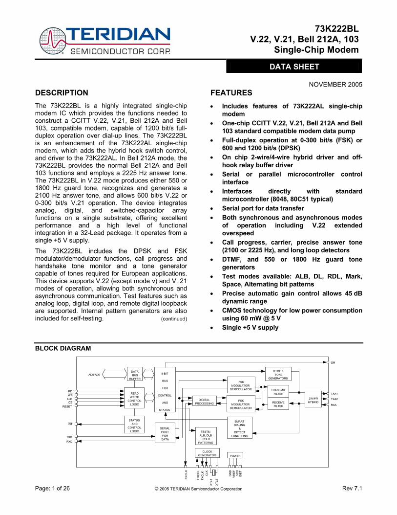
NOVEMBER 2005DESCRIPTION The 73K222BL is a highly integrated single-chip modem IC which provides the functions needed to construct a CCITT V.22, V.21, Bell 212A and Bell 103, compatible modem, capable of 1200 bit/s full-duplex operation over dial-up lines. The 73K222BL is an enhancement of the 73K222AL single-chip modem, which adds the hybrid hook switch control, and driver to the 73K222AL. In Bell 212A mode, the 73K222BL provides the normal Bell 212A and Bell 103 functions and employs a 2225 Hz answer tone. The 73K222BL in V.22 mode produces either 550 or 1800 Hz guard tone, recognizes and generates a 2100 Hz answer tone, and allows 600 bit/s V.22 or 0-300 bit/s V.21 operation. The device integrates analog, digital, and switched-capacitor array functions on a single substrate, offering excellent performance and a high level of functional integration in a 32-Lead package. It operates from a single +5 V supply. The 73K222BL includes the DPSK and FSK modulator/demodulator functions, call progress and handshake tone monitor and a tone generator capable of tones required for European applications. This device supports V.22 (except mode v) and V. 21 modes of operation, allowing both synchronous and asynchronous communication. Test features such as analog loop, digital loop, and remote digital loopback are supported. Internal pattern generators are also included for self-testing. (continued)
FEATURES • Includes features of 73K222AL single-chip
modem • One-chip CCITT V.22, V.21, Bell 212A and Bell
103 standard compatible modem data pump • Full-duplex operation at 0-300 bit/s (FSK) or
600 and 1200 bit/s (DPSK) • On chip 2-wire/4-wire hybrid driver and off-
hook relay buffer driver • Serial or parallel microcontroller control
interface • Interfaces directly with standard
microcontroller (8048, 80C51 typical) • Serial port for data transfer • Both synchronous and asynchronous modes
of operation including V.22 extended overspeed
• Call progress, carrier, precise answer tone (2100 or 2225 Hz), and long loop detectors
• DTMF, and 550 or 1800 Hz guard tone generators
• Test modes available: ALB, DL, RDL, Mark, Space, Alternating bit patterns
• Precise automatic gain control allows 45 dB dynamic range
• CMOS technology for low power consumption using 60 mW @ 5 V
• Single +5 V supply
BLOCK DIAGRAM
DIGITALPROCESSING
DTMF & TONE
GENERATORSFSK
MODULATOR/DEMODULATOR
PSKMODULATOR/
DEMODULATOR
SMARTDIALING
& DETECT
FUNCTIONS
POWER
TESTS:ALB, DLB
RDLBPATTERNS
TRANSMITFILTER
DATABUS
BUFFER
READWRITE
CONTROLLOGIC
STATUSAND
CONTROLLOGIC
8-BIT
BUS
FOR
CONTROL
AND
STATUS
SERIALPORTFOR
DATA
TXA1
RXA
ISE
TV
DD
VR
EF
GN
D
RX
CLK
CLOCKGENERATOR
XTL
2
XTL
1C
LKTX
CLK
EX
CLK
RDWR
ALECS
RESET
INT
TXDRXD
AD0-AD7
RECEIVEFILTER
2W/4WHYBRID
TXA2
OH
73K222BL
V.22, V.21, Bell 212A, 103 Single-Chip Modem with Integrated Hybrid
DATA SHEET
Page: 2 of 26 © 2005 TERIDIAN Semiconductor Corporation Rev 7.1
DESCRIPTION (continued) The 73K222BL is designed to appear to the systems designer as a microprocessor peripheral, and will easily interface with popular one-chip microprocessors (80C51 typical) for control of modem functions through its 8-bit multiplexed address/data bus. An ALE control line simplifies address demultiplexing. Data communications occurs through a separate serial port only. The 73K222BL is ideal for use in either free standing or integral system modem products where full-duplex 1200 bit/s data communications over the 2-wire switched telephone network is desired. Its high functionality, low power consumption and efficient packaging simplify design requirements and increase system reliability. A complete modem requires only the addition of the phone line interface, a control microprocessor, and RS-232 level converter for a typical system.
The 73K222BL is part of TERIDIAN Semiconductor’s K-Series family of single-chip modem products. These devices allow systems to be configured for higher speeds and Bell or CCITT operation with only a single component change.
FUNCTIONAL DESCRIPTION HYBRID AND RELAY DRIVER To make designs more cost effective and space efficient, the 73K222BL includes the 2-wire to 4-wire hybrid with sufficient drive to interface directly to the telecom coupling transformers. In addition, an off hook relay driver with 40 mA drive capability is also included to allow use of commonly available mechanical telecom relays.
ASYNCHRONOUS MODE Data transmission for the DPSK mode requires that data ultimately be transmitted in a synchronous fashion. The 73K222BL includes ASYNC/SYNC and SYNC/ASYNC converters, which delete or insert stop bits in order to transmit data within a ±0.01% rate. In asynchronous mode the serial data comes from the TXD pin into the ASYNC/SYNC converter. The ASYNC/SYNC converter accepts the data provided on the TXD pin which normally must be 1200 or 600 bit/s +1.0%, -2.5%. The converter will then insert or delete stop bits in order to output a signal that is 1200 or 600 bit/s ± 0.01% (± 0.01% is required synchronous data rate accuracy). The serial data stream from the ASYNC/SYNC converter is passed through the data scrambler and onto the analog modulator. The data scrambler can be bypassed under processor control when unscrambled data must be transmitted. The ASYNC/SYNC converter and the data scrambler are bypassed in all FSK modes. If serial input data contains a break signal through one character (including start and stop bits) the break will be extended to at least 2 • N + 3 bits long (where N is the number of transmitted bits/character).
73K222BL
V.22, V.21, Bell 212A, 103 Single-Chip Modem with Integrated Hybrid
DATA SHEET
Page: 3 of 26 © 2005 TERIDIAN Semiconductor Corporation Rev 7.1
Serial data from the demodulator is passed first through the data descrambler and then through the SYNC/ASYNC converter. The SYNC/ASYNC converter will re-insert any deleted stop bits and transmit output data at an intra-character rate (bit-to-bit timing) of no greater than 1219 bit/s. An incoming break signal (low through two characters) will be passed through without incorrectly inserting a stop bit. The SYNC/ASYNC converter also has an extended overspeed mode, which allows selection of an overspeed range of either +1% or +2.3%. In the extended overspeed mode, stop bits are output at 7/8 the normal width.
SYNCHRONOUS MODE The CCITT V.22 standard defines synchronous operation at 600 and 1200 bit/s. The Bell 212A standard defines synchronous operation only at 1200 bit/s. Operation is similar to that of the asynchronous mode except that data must be synchronized to a provided clock and no variation in data transfer rate is allowable. Serial input data appearing at TXD must be valid on the rising edge of TXCLK. TXCLK is an internally derived signal in internal mode and is connected internally to the RXCLK pin in slave mode. Receive data at the RXD pin is clocked out on the falling edge of RXCLK. The ASYNCH/SYNCH converter is bypassed when synchronous mode is selected and data is transmitted out at the same rate as it is input.
DPSK MODULATOR/DEMODULATOR
The 73K222BL modulates a serial bit stream into di-bit pairs that are represented by four possible phase shifts as prescribed by the Bell 212A or V.22 standards. The baseband signal is then filtered to reduce intersymbol interference on the bandlimited 2-wire telephone line. Transmission occurs using either a 1200 Hz (originate mode) or 2400 Hz carrier (answer mode). Demodulation is the reverse of the modulation process, with the incoming analog signal
eventually decoded into di-bits and converted back to a serial bit stream. The demodulator also recovers the clock, which was encoded into the analog signal during modulation. Demodulation occurs using either a 1200 Hz carrier (answer mode or ALB originate mode) or a 2400 Hz carrier (originate mode or ALB answer mode). The device uses a phase locked loop coherent demodulation technique for optimum receiver performance.
FSK MODULATOR/DEMODULATOR The FSK modulator produces a frequency modulated analog output signal using two discrete frequencies to represent the binary data. In Bell 103, the standard frequencies of 1270 and 1070 Hz (originate, mark and space) or 2225 and 2025 Hz (answer, mark and space) are used. V.21 mode uses 980 and 1180 Hz (originate, mark and space), or 1650 and 1850Hz (answer, mark and space). Demodulation involves detecting the received frequencies and decoding them into the appropriate binary value. The rate converter and scrambler/descrambler are bypassed in the Bell 103 or V.21 modes.
PASSBAND FILTERS AND EQUALIZERS High and low band filters are included to shape the amplitude and phase response of the transmit and receive signals and provide compromise delay equalization and rejection of out-of-band signals in the receive channel. Amplitude and phase equalization are necessary to compensate for distortion of the transmission line and to reduce intersymbol interference in the bandlimited receive signal. The transmit signal filtering approximates a 75% square root of raised Cosine frequency response characteristic.
AGC The automatic gain control maintains a signal level at the input to the demodulators, which is constant to within 1 dB. It corrects quickly for increases in signal which would cause clipping and provides a total receiver dynamic range of > 45 dB.
(continued)
73K222BL
V.22, V.21, Bell 212A, 103 Single-Chip Modem with Integrated Hybrid
DATA SHEET
Page: 4 of 26 © 2005 TERIDIAN Semiconductor Corporation Rev 7.1
FUNCTIONAL DESCRIPTION (continued) PARALLEL BUS INTERFACE Four 8-bit registers are provided for control, option select and status monitoring. These registers are addressed with the AD0, AD1, and AD2 multiplexed address lines (latched by ALE) and appear to a control microprocessor as four consecutive memory locations. Two control registers and the tone register are read/write memory. The detect register is read only and cannot be modified except by modem response to monitored parameters.
SPECIAL DETECT CIRCUITRY
The special detect circuitry monitors the received analog signal to determine status or presence of carrier, call-progress tones, answer tone and weak received signal (long loop condition). An unscrambled mark request signal is also detected when the received data out of the DPSK demodulator before the descrambler has been high for 165.5 ms ± 6.5 ms minimum. The appropriate detect register bit is set when one of these conditions changes and an interrupt is generated for all purposes except long loop. The interrupts are disabled (masked) when the enable interrupt bit is set to 0.
DTMF GENERATOR The DTMF generator will output one of 16 standard tone pairs determined by a 4-bit binary value and TX DTMF mode bit previously loaded into the tone register. Tone generation is initiated when the DTMF mode is selected using the tone register and the transmit enable (CR0 bit D1) is changed from 0 to 1.
73K222BL
V.22, V.21, Bell 212A, 103 Single-Chip Modem with Integrated Hybrid
DATA SHEET
Page: 5 of 26 © 2005 TERIDIAN Semiconductor Corporation Rev 7.1
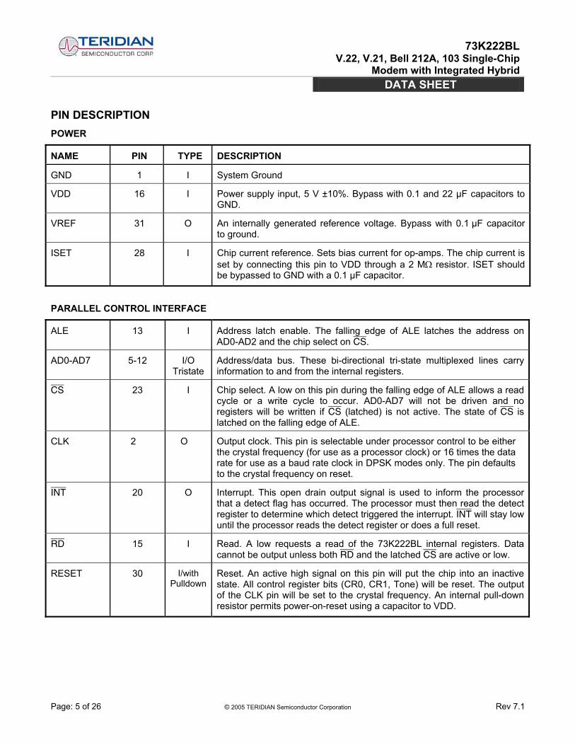
PIN DESCRIPTION POWER
NAME PIN TYPE DESCRIPTION
GND 1 I System Ground
VDD 16 I Power supply input, 5 V ±10%. Bypass with 0.1 and 22 µF capacitors to GND.
VREF 31 O An internally generated reference voltage. Bypass with 0.1 µF capacitor to ground.
ISET 28 I Chip current reference. Sets bias current for op-amps. The chip current is set by connecting this pin to VDD through a 2 MΩ resistor. ISET should be bypassed to GND with a 0.1 µF capacitor.
PARALLEL CONTROL INTERFACE
ALE 13 I Address latch enable. The falling edge of ALE latches the address on AD0-AD2 and the chip select on CS.
AD0-AD7 5-12 I/O Tristate
Address/data bus. These bi-directional tri-state multiplexed lines carry information to and from the internal registers.
CS 23 I Chip select. A low on this pin during the falling edge of ALE allows a read cycle or a write cycle to occur. AD0-AD7 will not be driven and no registers will be written if CS (latched) is not active. The state of CS is latched on the falling edge of ALE.
CLK 2 O Output clock. This pin is selectable under processor control to be either the crystal frequency (for use as a processor clock) or 16 times the data rate for use as a baud rate clock in DPSK modes only. The pin defaults to the crystal frequency on reset.
INT 20 O Interrupt. This open drain output signal is used to inform the processor that a detect flag has occurred. The processor must then read the detect register to determine which detect triggered the interrupt. INT will stay low until the processor reads the detect register or does a full reset.
RD 15 I Read. A low requests a read of the 73K222BL internal registers. Data cannot be output unless both RD and the latched CS are active or low.
RESET 30 I/with Pulldown
Reset. An active high signal on this pin will put the chip into an inactive state. All control register bits (CR0, CR1, Tone) will be reset. The output of the CLK pin will be set to the crystal frequency. An internal pull-down resistor permits power-on-reset using a capacitor to VDD.
73K222BL
V.22, V.21, Bell 212A, 103 Single-Chip Modem with Integrated Hybrid
DATA SHEET
Page: 6 of 26 © 2005 TERIDIAN Semiconductor Corporation Rev 7.1
PARALLEL CONTROL INTERFACE (continued)
NAME PIN TYPE DESCRIPTION
WR 14 I Write. A low on this pin informs the 73K222BL that data is available on AD0-AD7 for writing into an internal register. Data is latched on the rising edge of WR. No data is written unless both WR and the latched CS are low.
SERIAL CONTROL INTERFACE
NAME PIN TYPE DESCRIPTION
AD0-AD2 5-7 I Register Address Selection. These lines carry register addresses and should be valid during any read or write operation.
DATA (AD7) 12 I/O Serial Control Data. Data for a read/write operation is clocked in or out on the falling edge of the EXCLK pin. The direction of data flow is controlled by the RD pin. RD low outputs data. RD high inputs data.
RD 15 I Read. A low on this input informs the 73K222BL that data or status information is being read by the processor. The falling edge of the RD signal will initiate a read from the addressed register. The RD signal must continue fort eight falling edges of EXCLK in order to read all eight bits of the referenced register. Read data is provided LSB first. Data will not be output unless the RD signal is active.
WR 14 I Write. A low on this input informs the 73K222BL that data or status information has been shifted in through the DATA pin and is available for writing to an internal register. The normal procedure for a write is to shift in data LSB first on the DATA pin for eight consecutive falling edges of EXCLK and then to pulse WR low. Data is written on the rising edge of WR.
NOTE: The serial control mode is provided by tying ALE high and CS low. In this configuration AD7 becomes DATA and AD0, AD1 and AD2 become the address only.
73K222BL
V.22, V.21, Bell 212A, 103 Single-Chip Modem with Integrated Hybrid
DATA SHEET
Page: 7 of 26 © 2005 TERIDIAN Semiconductor Corporation Rev 7.1
DTE USER
NAME PIN TYPE DESCRIPTION
EXCLK 22 I External Clock. This signal is used in synchronous transmission when the external timing option has been selected. In the external timing mode the rising edge of EXCLK is used to strobe synchronous DPSK transmit data applied to on the TXD pin. Also used for serial control interface.
RXCLK 26 O Receive Clock. The falling edge of this clock output is coincident with the transitions in the serial received data output. The rising edge of RXCLK can be used to latch the valid output data. RXCLK will be valid as long as a carrier is present.
RXD 25 O/ Weak
Pull-up
Received Data Output. Serial receive data is available on this pin. The data is always valid on the rising edge of RXCLK when in synchronous mode. RXD will output constant marks if no carrier is detected.
TXCLK 21 O Transmit Clock. This signal is used in synchronous transmission to latch serial input data on the TXD pin. Data must be provided so that valid data is available on the rising edge of the TXCLK. The transmit clock is derived from different sources depending upon the synchronization mode selection. In internal mode the clock is generated internally. In external mode TXCLK is phase locked to the EXCLK pin. In slave mode TXCLK is phase locked to the RXCLK pin. TXCLK is always active.
TXD 24 I Transmit Data Input. Serial data for transmission is applied on this pin. In synchronous modes, the data must be valid on the rising edge of the TXCLK clock. In asynchronous modes (1200/600 bit/s or 300 baud) no clocking is necessary. DPSK data must be 1200/600 bit/s +1%, -2.5% or +2.3%, -2.5 % in extended over speed mode.
ANALOG INTERFACE AND OSCILLATOR
NAME PIN TYPE DESCRIPTION
RXA 32 I Received modulated analog signal input from the telephone line interface.
TXA1 TXA2
18 17
O Transmit analog output to the telephone line interface.
XTL1 XTL2
3 4
I I
These pins are for the internal crystal oscillator requiring an 11.0592 MHz parallel mode crystal. Load capacitors should be connected from XTL1 and XTL2 to ground. XTL2 can also be driven from an external clock.
OH 27 O Off-hook relay driver. This signal is an open drain output capable of sinking 40 mA and is used for controlling a relay. The output is the complement of the OH register bit in the ID Register.
73K222BL
V.22, V.21, Bell 212A, 103 Single-Chip Modem with Integrated Hybrid
DATA SHEET
Page: 8 of 26 © 2005 TERIDIAN Semiconductor Corporation Rev 7.1
REGISTER DESCRIPTIONS Four 8-bit internal registers are accessible for control and status monitoring. The registers are accessed in read or write operations by addressing AD0, AD1 and AD2 lines. The address lines are latched by ALE. Register CR0 controls the method by which data is transferred over the phone line. CR1 controls the interface between the microprocessor and the 73K222BL internal state.
DR is the Detect Register, which provides an indication of monitored modem status conditions. TR, the Tone Control Register, controls the DTMF generator, answer and guard tones and RXD output gate used in the modem initial connect sequence. All registers are read/write except for DR, which is read only. Register control and status bits are identified below:
REGISTER BIT SUMMARY
NOTE: When a register containing reserved control bits is written into, the reserved bits must be programmed as 0's.
X = Undefined, mask in software
MODULATION OPTION
00 = NORMAL01 = ANALOG LOOPBACK10 = REMOTE DIGITAL LOOPBACK11 = LOCAL DIGITAL LOOPBACK
CONTROLREGISTER 000
TRANSMITMODE
3
TRANSMITMODE
2
TRANSMITMODE
1
TRANSMITENABLE
ORIGINATE/ANSWER
DATA BIT NUMBER
AD2 - AD0REGISTER
ADDRESS
D7 D6 D5 D4 D3 D2 D1 D0
TESTMODE
0
TESTMODE
1RESETCLK
CONTROLBYPASS
SCRAMBLER
ENABLEDETECT
INTERRUPT
TRANSMITPATTERN
0
TRANSMITPATTERN
1001
CONTROLREGISTER CR1
LONGLOOP
CALLPROGRESS
ANSWERTONE
CARRIERDETECT
RECEIVEDATA010
DETECTREGISTER DR
DTMF0/GUARD/
ANSWER/TONE
DTMF1/OVERSPEEDDTMF2DTMF3TRANSMIT
DTMF
TRANSMITANSWER
TONE
RXDOUTPUT
CONTROL011
TONECONTROLREGISTER
TR
TRANSMITMODE
0
0000 = PWR DOWN0001 = INT SYNCH0010 = EXT SYNCH0011 = SLAVE SYNCH0100 = ASYNCH 8 BITS/CHAR0101 = ASYNCH 9 BITS/CHAR0110 = ASYNCH 10 BITS/CHAR0111 = ASYNCH 11 BITS/CHAR1100 = FSK
0 = DISABLE TXA OUTPUT1 = ENABLE TXA OUTPUT
0 = ANSWER1 = ORIGINATE
00 = TX DATA01 = TX ALTERNATE10 = TX MARK11 = TX SPACE
0 = DISABLE1 = ENABLE
0 = NORMAL1 = BYPASS SCRAMBLER
0 = XTAL1 = 16 X DATARATE OUTPUT AT CLK PIN INDPSK MODEONLY
0 = NORMAL1 = RESET
OUTPUTSRECEIVEDDATA STREAM
0 = CONDITION NOT DETECTED1 = CONDITION DETECTED
RXD PIN0 = NORMAL1 = WEAK PULL-UP
0 = OFF1 = ON
0 = Disable DTMF1 = TX DTMF
4 BIT CODE FOR 1 OF 16DUAL TONE COMBINATIONS
CR0
0 = 1200 BIT/S DPSK1 = 600 BIT/S DPSK0 = BELL 103 FSK1 = V.21 FSK
TRANSMITGUARD/TONE
0 = 2225 Hz A.T. 1800 Hz G.T.1 = 2100 Hz A.T. 500 Hz G.T.
0 = OFF1 = ON
UNSCR.MARKS
IDREGISTER 10 110 1 0 X OH
0
XX
X X X X
X = Undefined, mask in software 0 = OH Relay driver open1 = OH Open drain driver pulling low
1
0
00XX = 73K212AL, 322L, 321L01XX = 73K221AL, 302L10XX = 73K222AL, 222BL1100 = 73K224L, 224BL1110 = 73K324L, 324BL
73K222BL
V.22, V.21, Bell 212A, 103 Single-Chip Modem with Integrated Hybrid
DATA SHEET
Page: 9 of 26 © 2005 TERIDIAN Semiconductor Corporation Rev 7.1
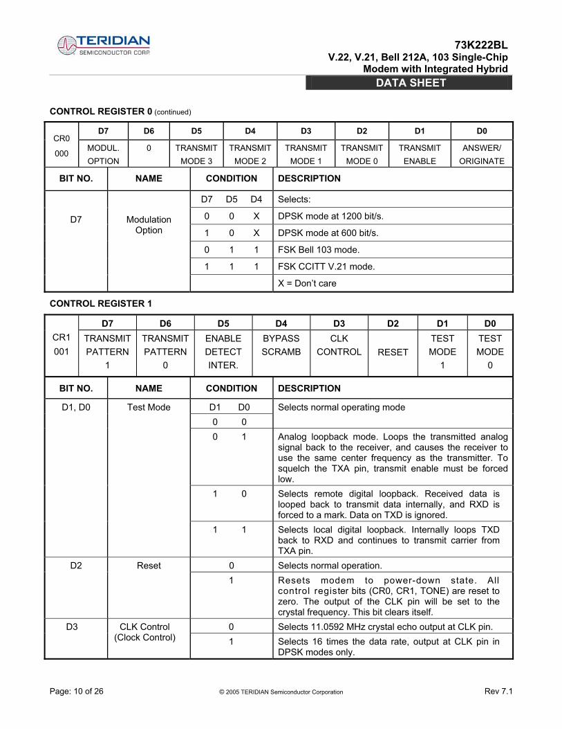
CONTROL REGISTER 0
D7 D6 D5 D4 D3 D2 D1 D0 CR0
000 MODUL. OPTION
0
TRANSMIT MODE 3
TRANSMIT MODE 2
TRANSMIT MODE 1
TRANSMIT MODE 0
TRANSMIT ENABLE
ANSWER/ ORIGINATE
BIT NO. NAME CONDITION DESCRIPTION
0 Selects answer mode (transmit in high band, receivein low band).
D0 Answer/ Originate
1 Selects originate mode (transmit in low band, receive in high band).
0 Disables transmit output at TXA. D1 Transmit Enable
1 Enables transmit output at TXA. Note: TX Enable must be set to 1 to allow Answer Tone and DTMF Transmission as well as data carriers.
D5 D4 D3 D2
0 0 0 0
Selects power-down mode. All functions disabled except digital interface.
0 0 0 1 Internal synchronous mode. In this mode TXCLK is an internally derived 1200 Hz signal. Serial input data appearing at TXD must be valid on the rising edge of TXCLK. Receive data is clocked out of RXD on the falling edge of RXCLK.
0 0 1 0 External synchronous mode. Operation is identical to internal synchronous, but TXCLK is connected internally to EXCLK pin, and a 1200 Hz ± 0.01% clock must be supplied externally.
0 0 1 1 Slave synchronous mode. Same operation as other synchronous modes. TXCLK is connected internally to the RXCLK pin in this mode.
0 1 0 0 Selects PSK asynchronous mode - 8 bits/character (1 start bit, 6 data bits, 1 stop bit).
0 1 0 1 Selects PSK asynchronous mode - 9 bits/character (1 start bit, 7 data bits, 1 stop bit).
0 1 1 0 Selects PSK asynchronous mode - 10 bits/character (1 start bit, 8 data bits, 1 stop bit).
0 1 1 1 Selects PSK asynchronous mode - 11 bits/character (1 start bit, 8 data bits, Parity and 1 or 2 stop bits).
D5, D4, D3, D2 Transmit Mode
1 1 0 0 Selects FSK operation.
D6 0 Not used; must be written as a “0.”
73K222BL
V.22, V.21, Bell 212A, 103 Single-Chip Modem with Integrated Hybrid
DATA SHEET
Page: 10 of 26 © 2005 TERIDIAN Semiconductor Corporation Rev 7.1
CONTROL REGISTER 0 (continued)
D7 D6 D5 D4 D3 D2 D1 D0 CR0
000 MODUL. OPTION
0 TRANSMIT MODE 3
TRANSMIT MODE 2
TRANSMIT MODE 1
TRANSMIT MODE 0
TRANSMIT ENABLE
ANSWER/ ORIGINATE
BIT NO. NAME CONDITION DESCRIPTION
D7 D5 D4 Selects:
0 0 X DPSK mode at 1200 bit/s.
1 0 X DPSK mode at 600 bit/s.
0 1 1 FSK Bell 103 mode.
1 1 1 FSK CCITT V.21 mode.
D7 Modulation Option
X = Don’t care
CONTROL REGISTER 1
D7 D6 D5 D4 D3 D2 D1 D0 CR1 001
TRANSMIT PATTERN
1
TRANSMIT PATTERN
0
ENABLE DETECT INTER.
BYPASS SCRAMB
CLK CONTROL RESET
TEST MODE
1
TEST MODE
0
BIT NO. NAME CONDITION DESCRIPTION
D1 D0 0 0
Selects normal operating mode
0 1 Analog loopback mode. Loops the transmitted analog signal back to the receiver, and causes the receiver to use the same center frequency as the transmitter. To squelch the TXA pin, transmit enable must be forced low.
1 0 Selects remote digital loopback. Received data is looped back to transmit data internally, and RXD is forced to a mark. Data on TXD is ignored.
D1, D0 Test Mode
1 1 Selects local digital loopback. Internally loops TXD back to RXD and continues to transmit carrier from TXA pin.
0 Selects normal operation. D2 Reset 1 Resets modem to power-down state. All
control register bits (CR0, CR1, TONE) are reset to zero. The output of the CLK pin will be set to the crystal frequency. This bit clears itself.
0 Selects 11.0592 MHz crystal echo output at CLK pin. D3 CLK Control (Clock Control) 1 Selects 16 times the data rate, output at CLK pin in
DPSK modes only.
73K222BL
V.22, V.21, Bell 212A, 103 Single-Chip Modem with Integrated Hybrid
DATA SHEET
Page: 11 of 26 © 2005 TERIDIAN Semiconductor Corporation Rev 7.1
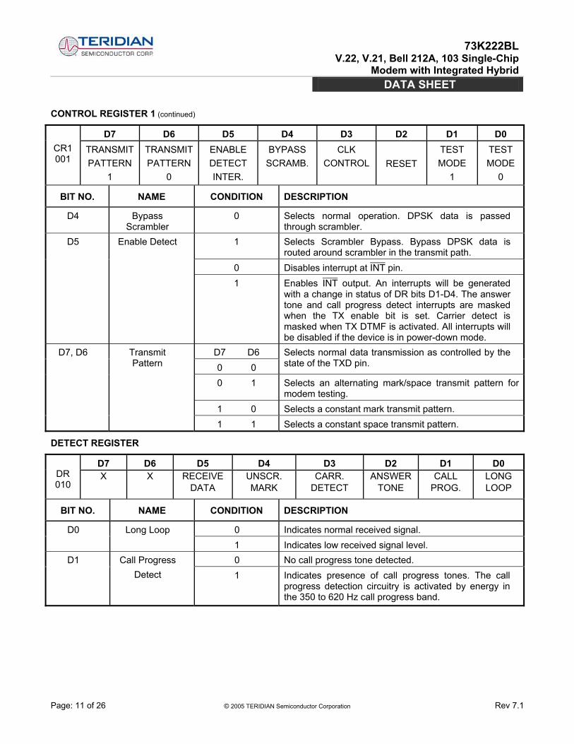
CONTROL REGISTER 1 (continued)
D7 D6 D5 D4 D3 D2 D1 D0 CR1 001
TRANSMIT PATTERN
1
TRANSMIT PATTERN
0
ENABLE DETECT INTER.
BYPASS SCRAMB.
CLK CONTROL RESET
TEST MODE
1
TEST MODE
0
BIT NO. NAME CONDITION DESCRIPTION
D4 Bypass Scrambler
0 Selects normal operation. DPSK data is passed through scrambler.
1 Selects Scrambler Bypass. Bypass DPSK data is routed around scrambler in the transmit path.
0 Disables interrupt at INT pin.
D5 Enable Detect
1 Enables INT output. An interrupts will be generated with a change in status of DR bits D1-D4. The answer tone and call progress detect interrupts are masked when the TX enable bit is set. Carrier detect is masked when TX DTMF is activated. All interrupts will be disabled if the device is in power-down mode.
D7 D6 0 0
Selects normal data transmission as controlled by the state of the TXD pin.
0 1 Selects an alternating mark/space transmit pattern for modem testing.
1 0 Selects a constant mark transmit pattern.
D7, D6 Transmit Pattern
1 1 Selects a constant space transmit pattern.
DETECT REGISTER
D7 D6 D5 D4 D3 D2 D1 D0 DR 010
X X RECEIVE DATA
UNSCR. MARK
CARR. DETECT
ANSWER TONE
CALL PROG.
LONG LOOP
BIT NO. NAME CONDITION DESCRIPTION
0 Indicates normal received signal. D0 Long Loop 1 Indicates low received signal level. 0 No call progress tone detected. D1 Call Progress
Detect 1 Indicates presence of call progress tones. The call progress detection circuitry is activated by energy in the 350 to 620 Hz call progress band.
73K222BL
V.22, V.21, Bell 212A, 103 Single-Chip Modem with Integrated Hybrid
DATA SHEET
Page: 12 of 26 © 2005 TERIDIAN Semiconductor Corporation Rev 7.1
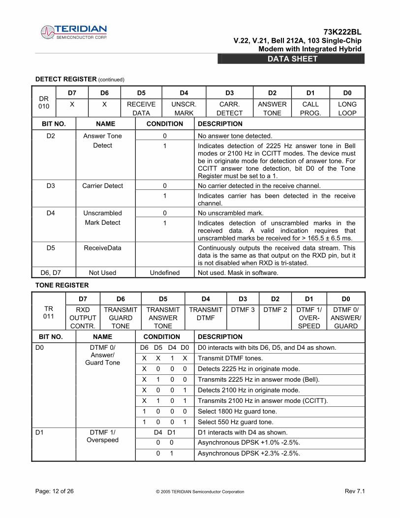
DETECT REGISTER (continued)
D7 D6 D5 D4 D3 D2 D1 D0 DR 010 X X RECEIVE
DATA UNSCR. MARK
CARR. DETECT
ANSWER TONE
CALL PROG.
LONG LOOP
BIT NO. NAME CONDITION DESCRIPTION
0 No answer tone detected. D2 Answer Tone Detect 1 Indicates detection of 2225 Hz answer tone in Bell
modes or 2100 Hz in CCITT modes. The device must be in originate mode for detection of answer tone. For CCITT answer tone detection, bit D0 of the Tone Register must be set to a 1.
0 No carrier detected in the receive channel. D3 Carrier Detect 1 Indicates carrier has been detected in the receive
channel. 0 No unscrambled mark. D4 Unscrambled
Mark Detect 1 Indicates detection of unscrambled marks in the received data. A valid indication requires that unscrambled marks be received for > 165.5 ± 6.5 ms.
D5 ReceiveData Continuously outputs the received data stream. This data is the same as that output on the RXD pin, but it is not disabled when RXD is tri-stated.
D6, D7 Not Used Undefined Not used. Mask in software.
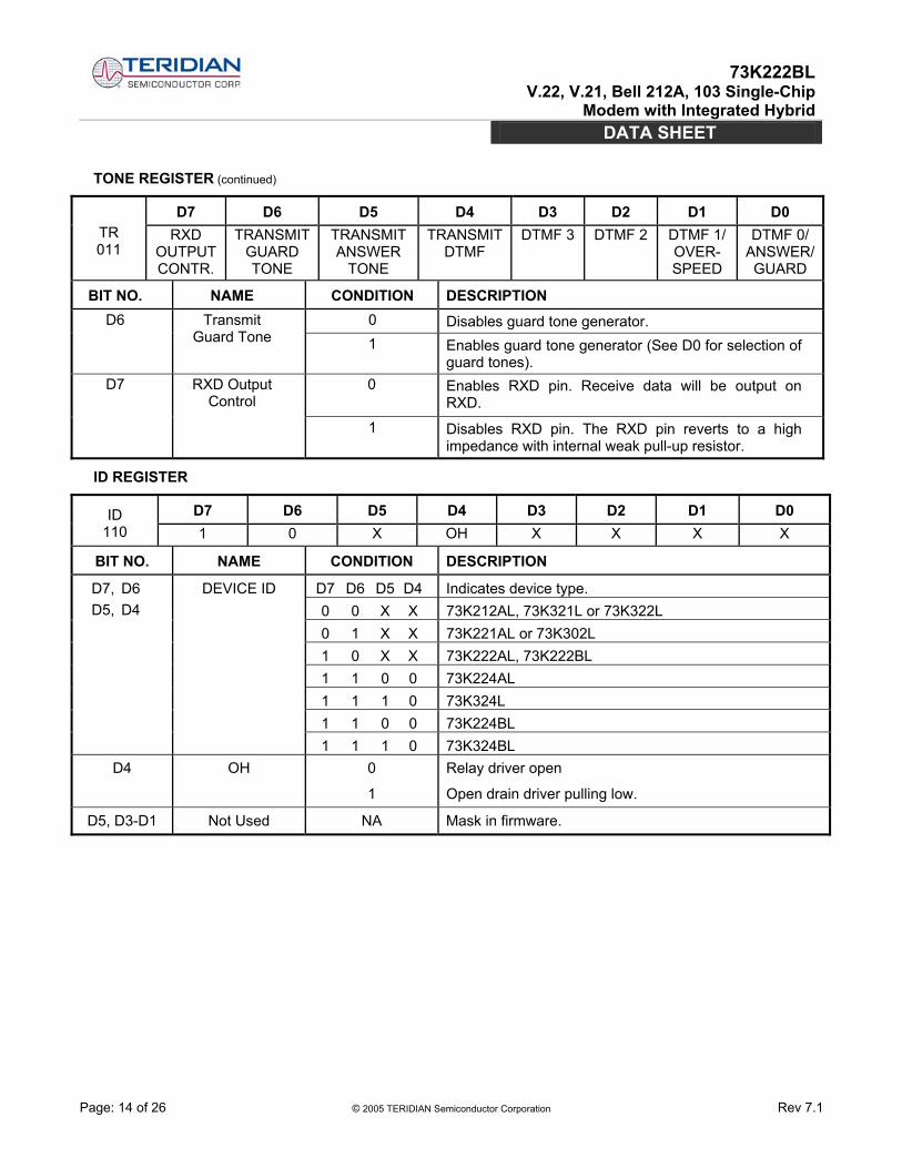
TONE REGISTER
D7 D6 D5 D4 D3 D2 D1 D0 TR 011
RXD OUTPUT CONTR.
TRANSMIT GUARD TONE
TRANSMIT ANSWER
TONE
TRANSMIT DTMF
DTMF 3 DTMF 2 DTMF 1/ OVER- SPEED
DTMF 0/ ANSWER/GUARD
BIT NO. NAME CONDITION DESCRIPTION D6 D5 D4 D0 D0 interacts with bits D6, D5, and D4 as shown. X X 1 X Transmit DTMF tones. X 0 0 0 Detects 2225 Hz in originate mode. X 1 0 0 Transmits 2225 Hz in answer mode (Bell). X 0 0 1 Detects 2100 Hz in originate mode. X 1 0 1 Transmits 2100 Hz in answer mode (CCITT). 1 0 0 0 Select 1800 Hz guard tone.
D0 DTMF 0/ Answer/
Guard Tone
1 0 0 1 Select 550 Hz guard tone. D4 D1 D1 interacts with D4 as shown. 0 0 Asynchronous DPSK +1.0% -2.5%.
D1 DTMF 1/ Overspeed
0 1 Asynchronous DPSK +2.3% -2.5%.
73K222BL
V.22, V.21, Bell 212A, 103 Single-Chip Modem with Integrated Hybrid
DATA SHEET
Page: 13 of 26 © 2005 TERIDIAN Semiconductor Corporation Rev 7.1
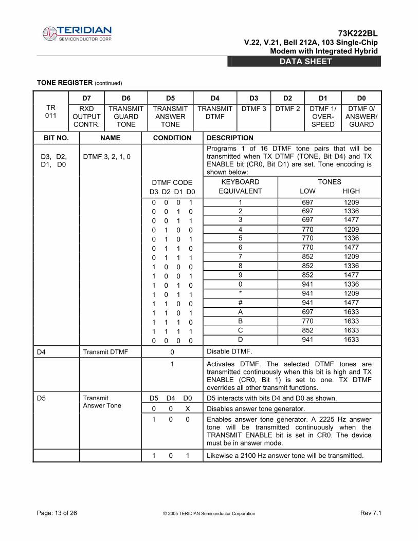
TONE REGISTER (continued)
D7 D6 D5 D4 D3 D2 D1 D0 TR 011
RXD OUTPUT CONTR.
TRANSMIT GUARD TONE
TRANSMIT ANSWER
TONE
TRANSMIT DTMF
DTMF 3 DTMF 2 DTMF 1/ OVER- SPEED
DTMF 0/ ANSWER/GUARD
BIT NO. NAME CONDITION DESCRIPTION Programs 1 of 16 DTMF tone pairs that will be transmitted when TX DTMF (TONE, Bit D4) and TX ENABLE bit (CR0, Bit D1) are set. Tone encoding is shown below:
DTMF CODE D3 D2 D1 D0
KEYBOARD EQUIVALENT
TONES LOW HIGH
1 697 1209 2 697 1336 3 697 1477 4 770 1209 5 770 1336 6 770 1477 7 852 1209 8 852 1336 9 852 1477 0 941 1336 * 941 1209 # 941 1477 A 697 1633 B 770 1633 C 852 1633
D3, D2, D1, D0
DTMF 3, 2, 1, 0
0 0 0 1 0 0 1 0 0 0 1 1 0 1 0 0 0 1 0 1 0 1 1 0 0 1 1 1 1 0 0 0 1 0 0 1 1 0 1 0 1 0 1 1 1 1 0 0 1 1 0 1 1 1 1 0 1 1 1 1 0 0 0 0 D 941 1633
D4 Transmit DTMF 0 Disable DTMF.
1 Activates DTMF. The selected DTMF tones are transmitted continuously when this bit is high and TX ENABLE (CR0, Bit 1) is set to one. TX DTMF overrides all other transmit functions.
D5 D4 D0 D5 interacts with bits D4 and D0 as shown. 0 0 X Disables answer tone generator.
D5 Transmit Answer Tone
1 0 0 Enables answer tone generator. A 2225 Hz answer tone will be transmitted continuously when the TRANSMIT ENABLE bit is set in CR0. The device must be in answer mode.
1 0 1 Likewise a 2100 Hz answer tone will be transmitted.
73K222BL
V.22, V.21, Bell 212A, 103 Single-Chip Modem with Integrated Hybrid
DATA SHEET
Page: 14 of 26 © 2005 TERIDIAN Semiconductor Corporation Rev 7.1
TONE REGISTER (continued)
D7 D6 D5 D4 D3 D2 D1 D0 TR 011
RXD OUTPUT CONTR.
TRANSMIT GUARD TONE
TRANSMIT ANSWER
TONE
TRANSMIT DTMF
DTMF 3 DTMF 2 DTMF 1/ OVER- SPEED
DTMF 0/ ANSWER/GUARD
BIT NO. NAME CONDITION DESCRIPTION 0 Disables guard tone generator. D6 Transmit
Guard Tone 1 Enables guard tone generator (See D0 for selection of guard tones).
0 Enables RXD pin. Receive data will be output on RXD.
D7 RXD Output Control
1 Disables RXD pin. The RXD pin reverts to a high impedance with internal weak pull-up resistor.
ID REGISTER
D7 D6 D5 D4 D3 D2 D1 D0 ID 110 1 0 X OH X X X X
BIT NO. NAME CONDITION DESCRIPTION
D7 D6 D5 D4 Indicates device type. 0 0 X X 73K212AL, 73K321L or 73K322L 0 1 X X 73K221AL or 73K302L 1 0 X X 73K222AL, 73K222BL 1 1 0 0 73K224AL 1 1 1 0 73K324L 1 1 0 0 73K224BL
D7, D6 D5, D4
DEVICE ID
1 1 1 0 73K324BL D4 OH 0
1
Relay driver open
Open drain driver pulling low.
D5, D3-D1 Not Used NA Mask in firmware.
73K222BL
V.22, V.21, Bell 212A, 103 Single-Chip Modem with Integrated Hybrid
DATA SHEET
Page: 15 of 26 © 2005 TERIDIAN Semiconductor Corporation Rev 7.1
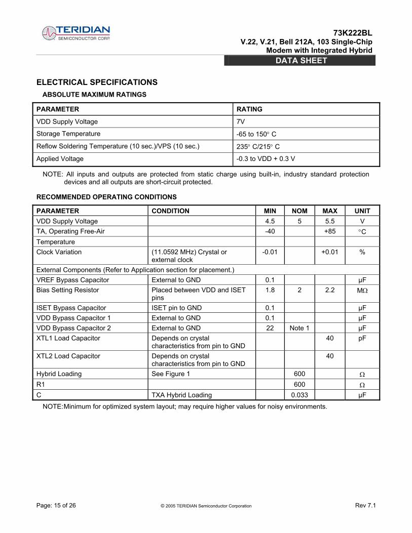
ELECTRICAL SPECIFICATIONS ABSOLUTE MAXIMUM RATINGS
PARAMETER RATING
VDD Supply Voltage 7V
Storage Temperature -65 to 150° C
Reflow Soldering Temperature (10 sec.)/VPS (10 sec.) 235° C/215° C
Applied Voltage -0.3 to VDD + 0.3 V
NOTE: All inputs and outputs are protected from static charge using built-in, industry standard protection devices and all outputs are short-circuit protected.
RECOMMENDED OPERATING CONDITIONS
PARAMETER CONDITION MIN NOM MAX UNIT VDD Supply Voltage 4.5 5 5.5 V TA, Operating Free-Air -40 +85 °C Temperature Clock Variation (11.0592 MHz) Crystal or
external clock -0.01 +0.01 %
External Components (Refer to Application section for placement.) VREF Bypass Capacitor External to GND 0.1 µF Bias Setting Resistor Placed between VDD and ISET
pins 1.8 2 2.2 MΩ
ISET Bypass Capacitor ISET pin to GND 0.1 µF VDD Bypass Capacitor 1 External to GND 0.1 µF VDD Bypass Capacitor 2 External to GND 22 Note 1 µF XTL1 Load Capacitor Depends on crystal
characteristics from pin to GND 40 pF
XTL2 Load Capacitor Depends on crystal characteristics from pin to GND
40
Hybrid Loading See Figure 1 600 Ω R1 600 Ω C TXA Hybrid Loading 0.033 µF
NOTE: Minimum for optimized system layout; may require higher values for noisy environments.
73K222BL
V.22, V.21, Bell 212A, 103 Single-Chip Modem with Integrated Hybrid
DATA SHEET
Page: 16 of 26 © 2005 TERIDIAN Semiconductor Corporation Rev 7.1
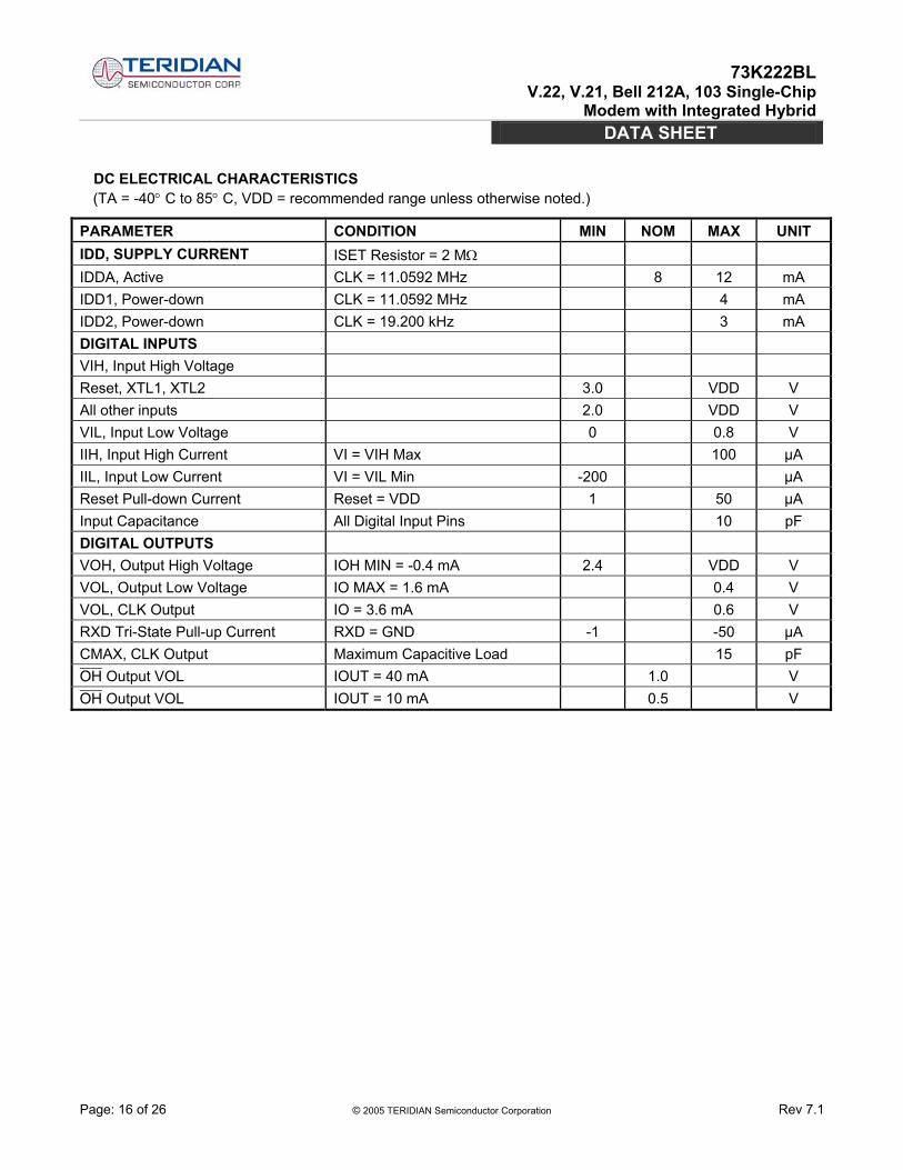
DC ELECTRICAL CHARACTERISTICS (TA = -40° C to 85° C, VDD = recommended range unless otherwise noted.)
PARAMETER CONDITION MIN NOM MAX UNIT IDD, SUPPLY CURRENT ISET Resistor = 2 MΩ IDDA, Active CLK = 11.0592 MHz 8 12 mA IDD1, Power-down CLK = 11.0592 MHz 4 mA IDD2, Power-down CLK = 19.200 kHz 3 mA DIGITAL INPUTS VIH, Input High Voltage Reset, XTL1, XTL2 3.0 VDD V All other inputs 2.0 VDD V VIL, Input Low Voltage 0 0.8 V IIH, Input High Current VI = VIH Max 100 µA IIL, Input Low Current VI = VIL Min -200 µA Reset Pull-down Current Reset = VDD 1 50 µA Input Capacitance All Digital Input Pins 10 pF DIGITAL OUTPUTS VOH, Output High Voltage IOH MIN = -0.4 mA 2.4 VDD V VOL, Output Low Voltage IO MAX = 1.6 mA 0.4 V VOL, CLK Output IO = 3.6 mA 0.6 V RXD Tri-State Pull-up Current RXD = GND -1 -50 µA CMAX, CLK Output Maximum Capacitive Load 15 pF OH Output VOL IOUT = 40 mA 1.0 V OH Output VOL IOUT = 10 mA 0.5 V
73K222BL
V.22, V.21, Bell 212A, 103 Single-Chip Modem with Integrated Hybrid
DATA SHEET
Page: 17 of 26 © 2005 TERIDIAN Semiconductor Corporation Rev 7.1
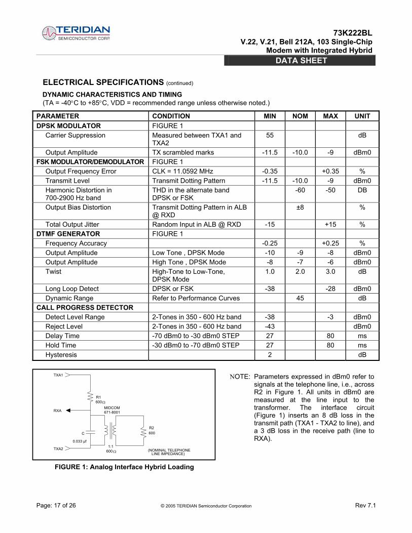
ELECTRICAL SPECIFICATIONS (continued) DYNAMIC CHARACTERISTICS AND TIMING (TA = -40°C to +85°C, VDD = recommended range unless otherwise noted.)
PARAMETER CONDITION MIN NOM MAX UNIT DPSK MODULATOR FIGURE 1 Carrier Suppression Measured between TXA1 and
TXA2 55 dB
Output Amplitude TX scrambled marks -11.5 -10.0 -9 dBm0 FSK MODULATOR/DEMODULATOR FIGURE 1 Output Frequency Error CLK = 11.0592 MHz -0.35 +0.35 % Transmit Level Transmit Dotting Pattern -11.5 -10.0 -9 dBm0 Harmonic Distortion in 700-2900 Hz band
THD in the alternate band DPSK or FSK
-60 -50 DB
Output Bias Distortion Transmit Dotting Pattern in ALB @ RXD
±8 %
Total Output Jitter Random Input in ALB @ RXD -15 +15 % DTMF GENERATOR FIGURE 1 Frequency Accuracy -0.25 +0.25 % Output Amplitude Low Tone , DPSK Mode -10 -9 -8 dBm0 Output Amplitude High Tone , DPSK Mode -8 -7 -6 dBm0 Twist High-Tone to Low-Tone,
DPSK Mode 1.0 2.0 3.0 dB
Long Loop Detect DPSK or FSK -38 -28 dBm0 Dynamic Range Refer to Performance Curves 45 dB CALL PROGRESS DETECTOR Detect Level Range 2-Tones in 350 - 600 Hz band -38 -3 dBm0 Reject Level 2-Tones in 350 - 600 Hz band -43 dBm0 Delay Time -70 dBm0 to -30 dBm0 STEP 27 80 ms Hold Time -30 dBm0 to -70 dBm0 STEP 27 80 ms Hysteresis 2 dB
FIGURE 1: Analog Interface Hybrid Loading
TXA1
R1
RXA
TXA2 1:1
600R2
(NOMINAL TELEPHONELINE IMPEDANCE)
C
600 Ω
600 Ω
MIDCOM671-8001
0.033 µf
NOTE: Parameters expressed in dBm0 refer tosignals at the telephone line, i.e., acrossR2 in Figure 1. All units in dBm0 aremeasured at the line input to thetransformer. The interface circuit(Figure 1) inserts an 8 dB loss in thetransmit path (TXA1 - TXA2 to line), anda 3 dB loss in the receive path (line toRXA).
73K222BL
V.22, V.21, Bell 212A, 103 Single-Chip Modem with Integrated Hybrid
DATA SHEET
Page: 18 of 26 © 2005 TERIDIAN Semiconductor Corporation Rev 7.1
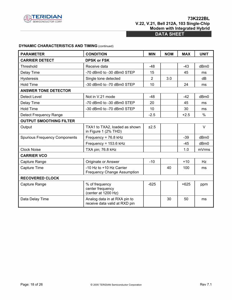
DYNAMIC CHARACTERISTICS AND TIMING (continued)
PARAMETER CONDITION MIN NOM MAX UNIT CARRIER DETECT DPSK or FSK Threshold Receive data -48 -43 dBm0 Delay Time -70 dBm0 to -30 dBm0 STEP 15 45 ms Hysteresis Single tone detected 2 3.0 dB Hold Time -30 dBm0 to -70 dBm0 STEP 10 24 ms ANSWER TONE DETECTOR Detect Level Not in V.21 mode -48 -42 dBm0 Delay Time -70 dBm0 to -30 dBm0 STEP 20 45 ms Hold Time -30 dBm0 to -70 dBm0 STEP 10 30 ms Detect Frequency Range -2.5 +2.5 % OUTPUT SMOOTHING FILTER Output TXA1 to TXA2, loaded as shown
in Figure 1 (2% THD) ±2.5 V
Frequency = 76.8 kHz -39 dBm0 Spurious Frequency Components Frequency = 153.6 kHz -45 dBm0
Clock Noise TXA pin; 76.8 kHz 1.0 mVrms CARRIER VCO Capture Range Originate or Answer -10 +10 Hz Capture Time -10 Hz to +10 Hz Carrier
Frequency Change Assumption 40 100 ms
RECOVERED CLOCK Capture Range % of frequency
center frequency (center at 1200 Hz)
-625 +625 ppm
Data Delay Time Analog data in at RXA pin to receive data valid at RXD pin
30 50 ms
73K222BL
V.22, V.21, Bell 212A, 103 Single-Chip Modem with Integrated Hybrid
DATA SHEET
Page: 19 of 26 © 2005 TERIDIAN Semiconductor Corporation Rev 7.1
DYNAMIC CHARACTERISTICS AND TIMING (continued)
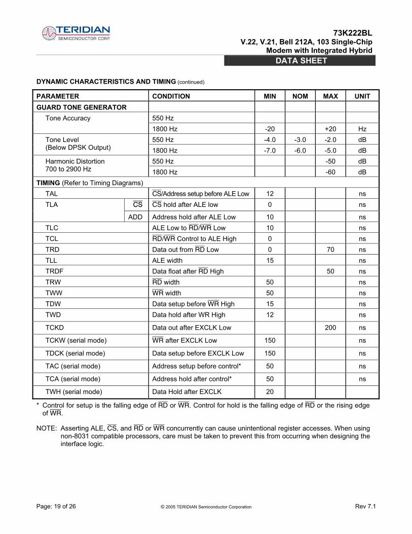
PARAMETER CONDITION MIN NOM MAX UNIT GUARD TONE GENERATOR
550 Hz Tone Accuracy 1800 Hz -20 +20 Hz 550 Hz -4.0 -3.0 -2.0 dB Tone Level
(Below DPSK Output) 1800 Hz -7.0 -6.0 -5.0 dB 550 Hz -50 dB Harmonic Distortion
700 to 2900 Hz 1800 Hz -60 dB TIMING (Refer to Timing Diagrams) TAL CS/Address setup before ALE Low 12 ns
CS CS hold after ALE low 0 ns TLA
ADD Address hold after ALE Low 10 ns TLC ALE Low to RD/WR Low 10 ns TCL RD/WR Control to ALE High 0 ns TRD Data out from RD Low 0 70 ns TLL ALE width 15 ns TRDF Data float after RD High 50 ns TRW RD width 50 ns TWW WR width 50 ns TDW Data setup before WR High 15 ns TWD Data hold after WR High 12 ns
TCKD Data out after EXCLK Low 200 ns
TCKW (serial mode) WR after EXCLK Low 150 ns
TDCK (serial mode) Data setup before EXCLK Low 150 ns
TAC (serial mode) Address setup before control* 50 ns
TCA (serial mode) Address hold after control* 50 ns
TWH (serial mode) Data Hold after EXCLK 20
* Control for setup is the falling edge of RD or WR. Control for hold is the falling edge of RD or the rising edge of WR.
NOTE: Asserting ALE, CS, and RD or WR concurrently can cause unintentional register accesses. When using non-8031 compatible processors, care must be taken to prevent this from occurring when designing the interface logic.
73K222BL
V.22, V.21, Bell 212A, 103 Single-Chip Modem with Integrated Hybrid
DATA SHEET
Page: 20 of 26 © 2005 TERIDIAN Semiconductor Corporation Rev 7.1
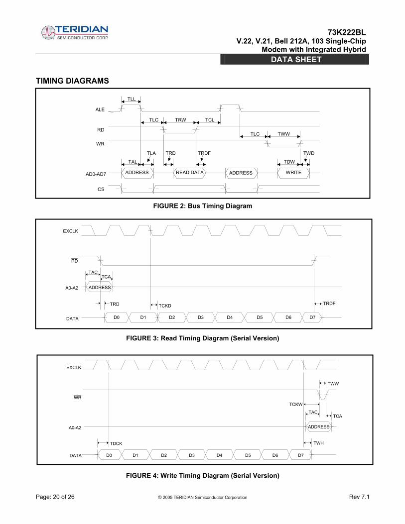
TIMING DIAGRAMS
FIGURE 2: Bus Timing Diagram
FIGURE 3: Read Timing Diagram (Serial Version)
FIGURE 4: Write Timing Diagram (Serial Version)
ALE
RD
WR
AD0-AD7
CS
ADDRESS READ DATA ADDRESS WRITE
TLL
TLC TRW TCL
TAL
TLA TRD TRDF
TLC TWW
TDW
TWD
TCA
ADDRESS
EXCLK
DATA
RD
A0-A2
D7D6D5D4D3D2D1D0
TAC
TRD TRDFTCKD
TWH
ADDRESS
TDCK
TCA
TWW
TCKW
A0-A2
DATA
EXCLK
WR
D7D6D5D4D3D2D1D0
TAC
73K222BL
V.22, V.21, Bell 212A, 103 Single-Chip Modem with Integrated Hybrid
DATA SHEET
Page: 21 of 26 © 2005 TERIDIAN Semiconductor Corporation Rev 7.1
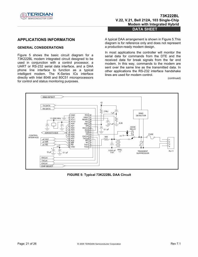
APPLICATIONS INFORMATION
GENERAL CONSIDERATIONS
Figure 5 shows the basic circuit diagram for a 73K222BL modem integrated circuit designed to be used in conjunction with a control processor, a UART or RS-232 serial data interface, and a DAA phone line interface to function as a typical intelligent modem. The K-Series ICs interface directly with Intel 8048 and 80C51 microprocessors for control and status monitoring purposes.
A typical DAA arrangement is shown in Figure 5.This diagram is for reference only and does not represent a production-ready modem design.
In most applications the controller will monitor the serial data for commands from the DTE and the received data for break signals from the far end modem. In this way, commands to the modem are sent over the same line as the transmitted data. In other applications the RS-232 interface handshake lines are used for modem control.
(continued)
FIGURE 5: Typical 73K222BL DAA Circuit
RXAVREF
RESETN/C
ISETOH
RXCLKRXD
TXCLKEXCLK
CSTXD
NCINT
TXA1TXA2
GNDCLKXTL1XTL2AD0AD1AD2AD3AD4AD5AD6AD7ALEWRRDVDD
123456789
10111213141516
ADR/DATA BUS
µC ALEµC WR
11.0592 MHz
323130
2625
2324
22
292827
2120191817
0.1 µF10 µF
++5
RXCLKTXCLKEXCLK
0.033 µFTYP.
600Ω1:1 TRANSIENT
SUPPRESSOR
FUSE+5600
0.1 µF
0.1 µF 8.2K
HOOKRELAY
1234
RJ-11
2 MΩ1 µF
+5
RING DETECT
TX DATA
RX DATA
CONTROLINTERFACE
CHIP SELECT
µC RD
RINGDETECTOR
73K222BL
V.22, V.21, Bell 212A, 103 Single-Chip Modem with Integrated Hybrid
DATA SHEET
Page: 22 of 26 © 2005 TERIDIAN Semiconductor Corporation Rev 7.1
APPLICATIONS INFORMATION (continued) DIRECT ACCESS ARRANGEMENT (DAA) The DAA (Direct Access Arrangement) required for the 73K222BL consists of an impedance matching resistor, telecom coupling transformer, and ring detection and fault protection circuitry.
The transformer specifications must comply with the impedance of the country in which the modem is being operated. Transformers designed specifically for use with the telephone network should be used. These may present a DC load to the network themselves (a “wet” transformer) or they may require AC coupling with a DC load provided by additional devices (a “dry” transformer). A dry transformer will generally provide higher performance and smaller size than a wet transformer. A wet transformer allows a simpler design, but must not saturate with the worst case DC current passing through it or distortion and poor performance will result.
The protection circuitry typically consists of a transient suppression device and current limiter to protect the user and the telephone network from hazardous voltages that can be present under fault conditions. The transient suppressor may be a MOV (metal oxide varistor), Sidactor (Teccor Electronics Inc.), spark gap device , or avalanche diode. Some devices clamp the transient to their specified break down voltage and others go into low impedance crowbar state. The latter require that the fault current to cease before they can return to their inactive state.
Current limiting devices can consist of a resistor, Raychem PolySwitch resettable fuse, or slow blow fuse that can withstand the transient tests without permanent damage or replacement.
Ring detection circuitry is not required by the FCC, but may be required by the application. The ring detector usually consists of an optoisolator, capacitor, and resistor to present the proper AC load to the network to meet the REN (Ring Equivalency Number) regulations of FCC Part 68. The K-Series Design Manual contains detailed information on the design of a ring detect circuits as well as the other topics concerning the DAA.
DESIGN CONSIDERATIONS
TERIDIAN Semiconductor's 1-chip modem products include all basic modem functions. This makes these devices adaptable for use in a variety of applications, and as easy to control as conventional digital bus peripherals.
Unlike digital logic circuitry, modem designs must properly contend with precise frequency tolerances and very low level analog signals, to ensure acceptable performance. Using good analog circuit design practices will generally result in a sound design. Following are additional recommendations, which should be taken into consideration when starting new designs.
CRYSTAL OSCILLATOR The K-Series crystal oscillator requires a parallel mode (antiresonant) crystal, which operates at 11.0592 MHz. It is important that this frequency be maintained to within ±0.01% accuracy.
In order for a parallel mode crystal to operate correctly and to specification, it must have a capacitor connected to the junction of each of the crystal and internal inverter connections, terminated to ground. The values of these capacitors depend primarily on the crystal’s characteristics, and to a lesser degree on the internal inverter circuit. The values used affect the accuracy and start up characteristics of the oscillator.
LAYOUT CONSIDERATIONS Good analog/digital design rules must be used to control system noise in order to obtain highest performance in modem designs. The more digital circuitry present on the PC board, the more this attention to noise control is needed. The modem should be treated as a high performance analog device. A 22 µF electrolytic capacitor in parallel with a 0.1 µF ceramic capacitor between VDD and GND is recommended. Liberal use of ground planes and larger traces on power and ground are also highly favored. High speed digital circuits tend to generate a significant amount of EMI (Electro-Magnetic Interference), which must be minimized in order to meet regulatory agency limitations. To accomplish this, high speed digital devices should be locally bypassed, and the telephone line interface and K-Series device should be located close to each other near the area of the board where the phone line connection is accessed.
73K222BL
V.22, V.21, Bell 212A, 103 Single-Chip Modem with Integrated Hybrid
DATA SHEET
Page: 23 of 26 © 2005 TERIDIAN Semiconductor Corporation Rev 7.1
To avoid problems, power supply and ground traces should be routed separately to the analog and digital functions on the board, and digital signals should not be routed near low level or high impedance analog traces. The analog and digital grounds should only connect at one point near the K-Series device ground pin to avoid ground loops. The K-Series modem ICs should have both high frequency and low frequency bypassing as close to the package as possible.
USING THE SERIAL MODE ON THE 73K2XXAL AND 73K222BL
A sensitivity to specific patterns being written to the control registers in the 73K212/221/222AL and 73K222BL modem data pumps has been seen on some parts when used in the serial control interface mode. An alternating pattern followed by its complement can cause the registers to not have the intended data correctly written to the registers. Specifically, if an alternating ..1010.. pattern is followed by its compliment, ..0101.., the register may instead be programmed with a ..0001.. pattern. After analysis, it has been found that any normal programming sequence should not include these steps with one exception, and that is in DTMF dialing. Since any random DTMF sequence could be dialed, there is the potential for these patterns to appear. For example, if a DTMF digit “5” , 0101 bin is followed by a DTMF digit “0” , 1010 bin, some parts will instead transmit a DTMF digit “8”, 1000 bin, in its place. The solution to this problem is to always clear the DTMF bits, D3-D0, between dialed digits. This will not add additional time to dialing since there is ample time between digits when the DTMF bits can be cleared. Previously during the DTMF off time the next digit would be loaded into the TONE register. It is now recommended to first clear bits D3-D0, then the next digit to be dialed is loaded into the DTMF bits.
As mentioned earlier, under normal circumstances these patterns would not be programmed for other registers. If for some reason other registers are programmed in such a way that an alternating pattern is followed by its compliment, those bits should be cleared before the complimentary pattern is sent.
This method has been tested over the entire voltage and temperature operating ranges. It has been found to be a reliable procedure to ensure the correct patterns are always programmed.
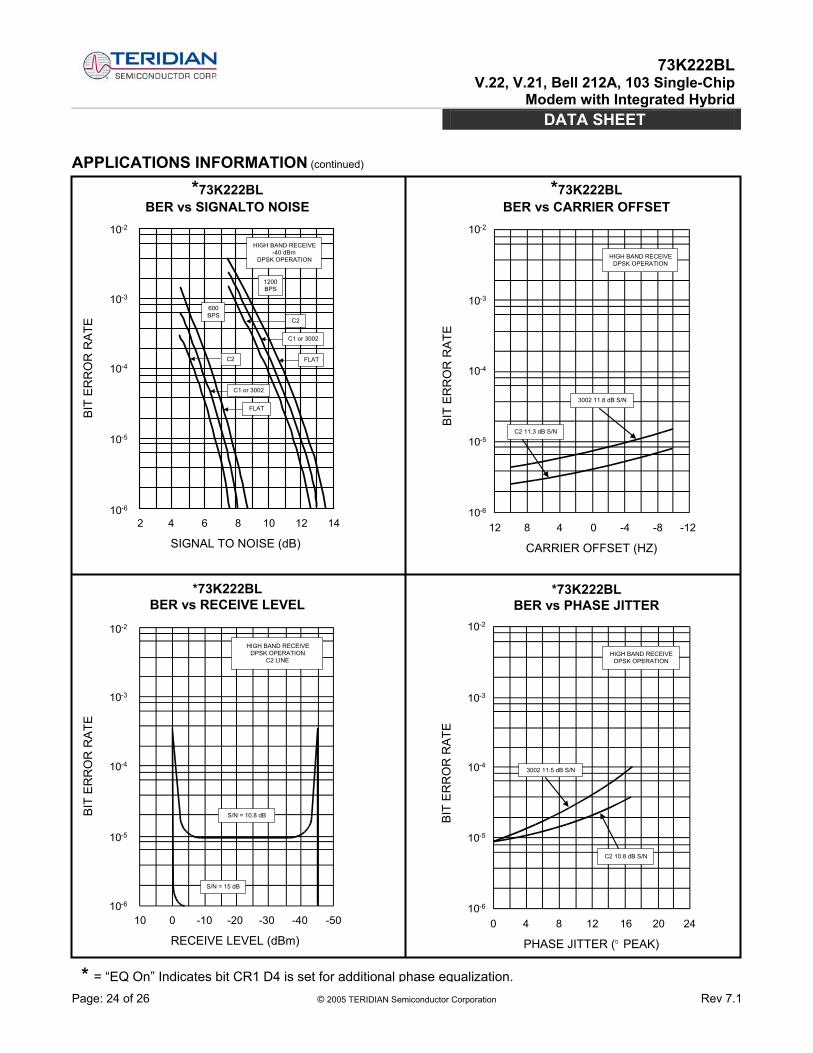
MODEM PERFORMANCE CHARACTERISTICS The curves presented here define modem IC performance under a variety of line conditions while inducing disturbances that are typical of those encountered during data transmission on public service telephone lines. Test data was taken using an AEA Electronics’ “Autotest I” modem test set and line simulator, operating under computer control. All tests were run full-duplex, using a Concord Data Systems 224 as the reference modem. A 511 pseudo-random-bit pattern was used for each data point. Noise was C-message weighted and all signal-to-noise (S/N) ratios reflect total power measurements similar to the CCITT V.56 measurement specification. The individual tests are defined as follows.
BER VS. S/N This test measures the ability of the modem to operate over noisy lines with a minimum of data-transfer errors. Since some noise is generated in the best of dial-up lines, the modem must operate with the lowest S/N ratio possible. Better modem performance is indicated by test curves that are closest to the BER axis. A narrow spread between curves representing the four line parameters indicates minimal variation in performance while operating over a range of operating conditions. Typically, a DPSK modem will exhibit better BER performance test curves receiving in the low band than in the high band.
BER VS. RECEIVE LEVEL This test measures the dynamic range of the modem. Because signal levels vary widely over dial-up lines, the widest possible dynamic range is desirable. The minimum Bell specification calls for 36 dB of dynamic range. S/N ratios are held constant at the indicated values while the receive level is lowered from a very high to very low signal levels. The width of the “bowl” of these curves, taken at the BER point, is the measure of dynamic range.
73K222BL
V.22, V.21, Bell 212A, 103 Single-Chip Modem with Integrated Hybrid
DATA SHEET
Page: 24 of 26 © 2005 TERIDIAN Semiconductor Corporation Rev 7.1
APPLICATIONS INFORMATION (continued)
*73K222BL BER vs SIGNALTO NOISE
*73K222BL
BER vs RECEIVE LEVEL
*73K222BL BER vs CARRIER OFFSET
*73K222BL
BER vs PHASE JITTER
HIGH BAND RECEIVE-40 dBm
DPSK OPERATION
1200BPS
C2
C1 or 3002
FLAT
600BPS
C2
C1 or 3002
FLAT
10-2
10-3
10-4
10-5
10-6
2 4 6 8 10 12 14
BIT
ERR
OR
RAT
E
SIGNAL TO NOISE (dB)
HIGH BAND RECEIVEDPSK OPERATION
C2 LINE
S/N = 10.8 dB
S/N = 15 dB
10-2
10-3
10-4
10-5
10-6
BIT
ERR
OR
RAT
E
10 0 -10 -20 -30 -40 -50
RECEIVE LEVEL (dBm)
HIGH BAND RECEIVEDPSK OPERATION
3002 11.8 dB S/N
C2 11.3 dB S/N
10-2
10-3
10-4
10-5
10-6
12 8 4 0 -4 -8 -12
BIT
ERR
OR
RAT
E
CARRIER OFFSET (HZ)
HIGH BAND RECEIVEDPSK OPERATION
3002 11.5 dB S/N
C2 10.8 dB S/N
10-2
10-3
10-4
10-5
10-6
BIT
ERR
OR
RAT
E
0 4 8 12 16 20 24
PHASE JITTER (° PEAK)
* = “EQ On” Indicates bit CR1 D4 is set for additional phase equalization.
73K222BL
V.22, V.21, Bell 212A, 103 Single-Chip Modem with Integrated Hybrid
DATA SHEET
Page: 25 of 26 © 2005 TERIDIAN Semiconductor Corporation Rev 7.1
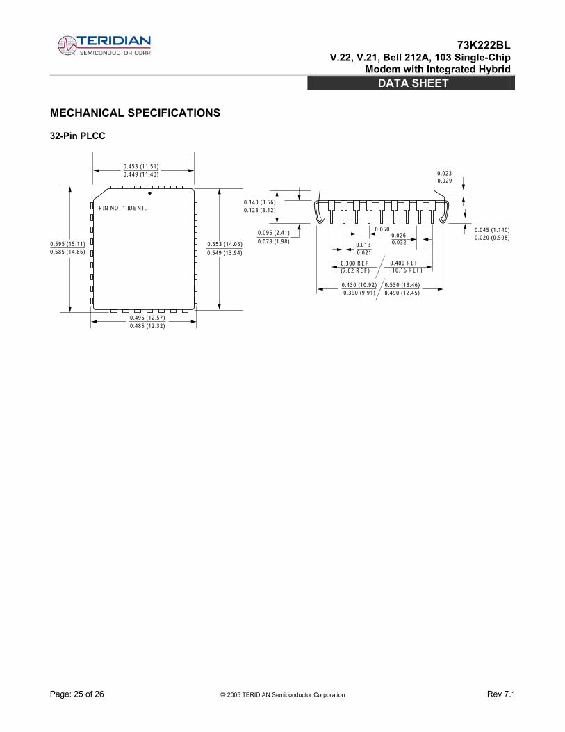
MECHANICAL SPECIFICATIONS
32-Pin PLCC
PIN NO. 1 IDENT.
0.595 (15.11)0.585 (14.86)
0.453 (11.51)0.449 (11.40)
0.553 (14.05)
0.549 (13.94)
0.0230.029
0.045 (1.140)0.020 (0.508)
0.050
0.013 0.021
0.026 0.032
0.495 (12.57)0.485 (12.32)
0.430 (10.92)0.390 (9.91)
0.530 (13.46)0.490 (12.45)
0.300 REF(7.62 REF)
0.400 REF(10.16 REF)
0.095 (2.41)
0.078 (1.98)
0.140 (3.56)0.123 (3.12)
73K222BL
V.22, V.21, Bell 212A, 103 Single-Chip Modem with Integrated Hybrid
DATA SHEET
Page: 26 of 26 © 2005 TERIDIAN Semiconductor Corporation Rev 7.1
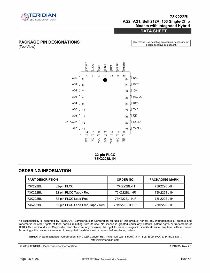
PACKAGE PIN DESIGNATIONS (Top View)
32-pin PLCC 73K222BL-IH
ORDERING INFORMATION
PART DESCRIPTION ORDER NO. PACKAGING MARK
73K222BL 32-pin PLCC 73K222BL-IH 73K222BL-IH
73K222BL 32-pin PLCC Tape / Reel 73K222BL-IHR 73K222BL-IH
73K222BL 32-pin PLCC Lead-Free 73K222BL-IH/F 73K222BL-IH
73K222BL 32-pin PLCC Lead-Free Tape / Reel 73K222BL-IHR/F 73K222BL-IH
No responsibility is assumed by TERIDIAN Semiconductor Corporation for use of this product nor for any infringements of patents and trademarks or other rights of third parties resulting from its use. No license is granted under any patents, patent rights or trademarks of TERIDIAN Semiconductor Corporation and the company reserves the right to make changes in specifications at any time without notice. Accordingly, the reader is cautioned to verify that the data sheet is current before placing orders.
TERIDIAN Semiconductor Corporation, 6440 Oak Canyon Rd., Irvine, CA 92618-5201, (714) 508-8800, FAX: (714) 508-8877, http://www.teridian.com
2005 TERIDIAN Semiconductor Corporation 11/10/05- Rev 7.1
AD0
AD1
AD2
AD3
AD4
AD5
AD6
DATA/AD7
ALE
XTA
L2
XTA
L1
CLK
GN
D
RX
A
VR
EF
RE
SE
T
N/C
ISET
OH
RXCLK
RXD
TXD
CS
EXCLK
TXCLK
WR
RD
VD
D
TXA
2
TXA
1
N/C
INT
4 3 2 1 32 31 305
6
7
8
9
10
11
12
13
29
28
27
26
25
24
23
22
2114 15 16 17 18 19 20
CAUTION: Use handling procedures necessary for a static sensitive component.