Embed Size (px)
Citation preview
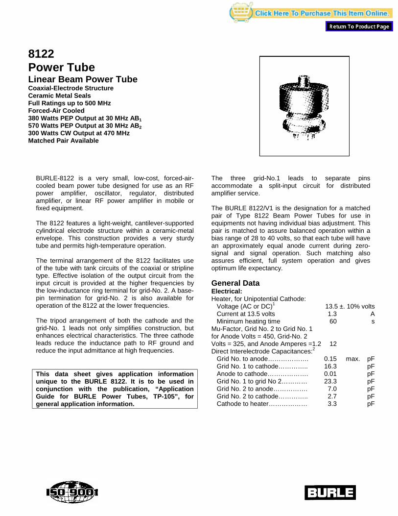
8122Power TubeLinear Beam Power TubeCoaxial-Electrode StructureCeramic Metal SealsFull Ratings up to 500 MHzForced-Air Cooled380 Watts PEP Output at 30 MHz AB1
570 Watts PEP Output at 30 MHz AB2
300 Watts CW Output at 470 MHzMatched Pair Available
BURLE-8122 is a very small, low-cost, forced-air-cooled beam power tube designed for use as an RFpower amplifier, oscillator, regulator, distributedamplifier, or linear RF power amplifier in mobile orfixed equipment.
The 8122 features a light-weight, cantilever-supportedcylindrical electrode structure within a ceramic-metalenvelope. This construction provides a very sturdytube and permits high-temperature operation.
The terminal arrangement of the 8122 facilitates useof the tube with tank circuits of the coaxial or striplinetype. Effective isolation of the output circuit from theinput circuit is provided at the higher frequencies bythe low-inductance ring terminal for grid-No. 2. A base-pin termination for grid-No. 2 is also available foroperation of the 8122 at the lower frequencies.
The tripod arrangement of both the cathode and thegrid-No. 1 leads not only simplifies construction, butenhances electrical characteristics. The three cathodeleads reduce the inductance path to RF ground andreduce the input admittance at high frequencies.
This data sheet gives application informationunique to the BURLE 8122. It is to be used inconjunction with the publication, “ApplicationGuide for BURLE Power Tubes, TP-105”, forgeneral application information.
The three grid-No.1 leads to separate pinsaccommodate a split-input circuit for distributedamplifier service.
The BURLE 8122/V1 is the designation for a matchedpair of Type 8122 Beam Power Tubes for use inequipments not having individual bias adjustment. Thispair is matched to assure balanced operation within abias range of 28 to 40 volts, so that each tube will havean approximately equal anode current during zero-signal and signal operation. Such matching alsoassures efficient, full system operation and givesoptimum life expectancy.
General DataElectrical:Heater, for Unipotential Cathode:
Voltage (AC or DC)1 13.5 ±. 10% voltsCurrent at 13.5 volts 1.3 AMinimum heating time 60 s
Mu-Factor, Grid No. 2 to Grid No. 1for Anode Volts = 450, Grid-No. 2Volts = 325, and Anode Amperes =1.2 12Direct Interelectrode Capacitances:2
Grid No. to anode………………. 0.15 max. pFGrid No. 1 to cathode………….. 16.3 pFAnode to cathode………………. 0.01 pFGrid No. 1 to grid No 2………… 23.3 pFGrid No. 2 to anode……………. 7.0 pFGrid No. 2 to cathode………….. 2.7 pFCathode to heater……………… 3.3 pF

Mechanical:Operating Position……………………………………….. AnyMaximum Overall Length………………………………. 2.26”Seated Length……………………………... 1.920” ± 0.065”Greatest Diameter………………………… 1.625” ± 0.015"Base…………….. Large-Wafer Elevenar 11-Pin with Ring
(JEDEC No. E11-81)Socket…………………. Jettronc No. CD77-030,
Johnsona No. 124-311-100,Erieb No. 9813-000, or equivalent
Grid No.2 BypassCapacitor………………
Johnsona No. 124-0113-001,Erieb No. 9812-000, or equivalent
Weight (Approx.)………………………………………. 3.5 oz
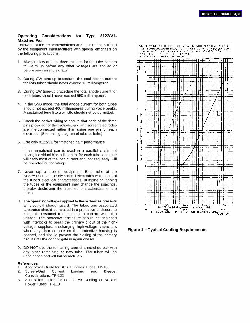
Thermal:Terminal Temperature (All terminals)….. 250 max ºCRadiator Core Temperature(See Dimensional Outline)……………… 250 max ºCAir Flow:
See Figure 1 - Typical Cooling Requirements
Linear RF Power AmplifierSingle-Sideband Suppressed-Carrier ServicePeak envelope conditions for a signal having a minimumpeak-to-average power ratio of 2Maximum CCS Ratings, Absolute-Maximum Values:DC Anode Voltage
Up to 30 MHz………………………... 30004 voltsUp to 500 MHz……………………… 2200 volts
Up to 500 MHzDC Grid-No. 2 Voltage………………... 400 voltsDC Grid-No. 1 Voltage……………….. -100 voltsDC Anode Current at PeakOf Envelope……………………………. 4505 mADC Grid-No. 1 Current……………….. 100 mAAnode Dissipation……………………. 400 wattsGrid-No. 2 Dissipation……………….. 8 wattsPeak Heater-Cathode Voltage
Heater negative with respectto cathode…………………………….. 150 voltsHeater positive with respect
to cathode…………………………….. 150 volts
Maximum Circuit Values:Grid No. 1 Circuit Resistance Under Any Condition:9
With fixed bias………………………….. 25,000 ohmsWith fixed bias (In Class AB1 operation 100,000 ohmsWith cathode bias…………………… Not recommended
Grid-No. 2 Circuit Impedance8………… 10,000 ohmsAnode Circuit Impedance……………… See Notes 4 and 6
Typical CCS Operation at 30 MHz with “Two-ToneModulation”:
AB1 AB2
DC Anode Voltage…………….. 2000 2500 voltsDC Grid-No. 2 Voltage………... 400 400 voltsDC Grid-No. 1 Voltage……….. -35 -35 voltsZero-Signal DC Anode Current 100 115 mAEffective RE Load Resistance.. 3050 3500 ohms
a. E. F. Johnson Co., 299 Johnson Ave., Waseca, MN 56093.b. Erie Specialty Products, 645W. 11th St., Erie, PA 16512.c. Jettron Products, Inc., 56 Route 10, Hanover, NJ 07936
DC Anode Current at Peakof Envelope…………………………
335 400 mA
Average DC Anode Current………. 250 275 mADC Grid-No. 2 Current atPeak of Envelope………………….. 10 6 mAAverage DC Grid-No 2 Current…… 7 4 mADC Grid-No. 1 Current atPeak of Envelope………………….. 0.057 3 mAPeak-Envelope Driver PowerOutput (Approx.)……………………. 0.3 0.5 wattOutput-Circuit Efficiency (Approx.).. 90 90 %Distortion Products Level:
Third order………………………... 2910 28 dbFifth order………………………… 32 32 db
Useful Power Output (Approx.)Average…………………………… 190 285 wattsPeak envelope…………………… 380 570 watts
RF Power Amplifier & Oscillator - Class CTelegraphy and RF Power Amplifier -Class C FM TelephonyMaximum CCS Ratings, Absolute-Maximum Values:
Up to 500 MHzDC Anode Voltage…………………………… 2200 voltsDC Grid-No. 2 Voltage………………………. 400 voltsDC Grid-No. 1 Voltage………………………. -100 voltsDC Anode Current…………………………… 300 mADC Grid-No. 1 Current………………………. 100 mAGrid-No. 2 Dissipation………………………. 8 wattsAnode Dissipation…………………………… 400 wattsPeak Heater-Cathode Voltage:
Heater negative with respectto cathode………………………………….. 150 volts
Heater positive with respectto cathode………………………………….. 150 volts
Maximum Circuit Values:Grid-No. 1 Circuit Resistance Under Any Condition:
With fixed bias………………………… 25,000 ohmsGrid-No. 2 Circuit Impedance………….. 10,000 ohmsAnode Circuit Impedance……………….. See Note 6
Typical CCS Operation:In Grid-Drive Circuit at 50 MHzDC Anode Voltage 700 1000 1500 1200 voltsDC Grid-No. 2 Voltage 175 200 200 200 voltsDC Grid-No. 1 Voltage -10 -30 -30 -30 voltsDC Anode Current 300 300 300 300 mADC Grid-No. 2 Current 25 20 20 20 mADC Grid-No. 1 Current 50 40 40 30 mADriver Power Output(Approx) 1.2 2 2 2 wattsUseful Power Output 120 175 275 375 watts
In Grid-Drive Circuit at 470 MHz
DC Anode Voltage 700 1000 1500 2000 voltsDC Grid-No. 2 Voltage 200 200 200 200 voltsDC Grid-No. 1 Voltage -30 -30 -30 -30 mADC Anode Current 300 300 300 300 mADC Grid-No. 2 Current 10 10 5 5 mADC Grid No. 1 Current 30 30 30 30 mADriver Power OutputApprox.) 5 5 5 5 wattsUseful Power Output 100 165 235 300 watts
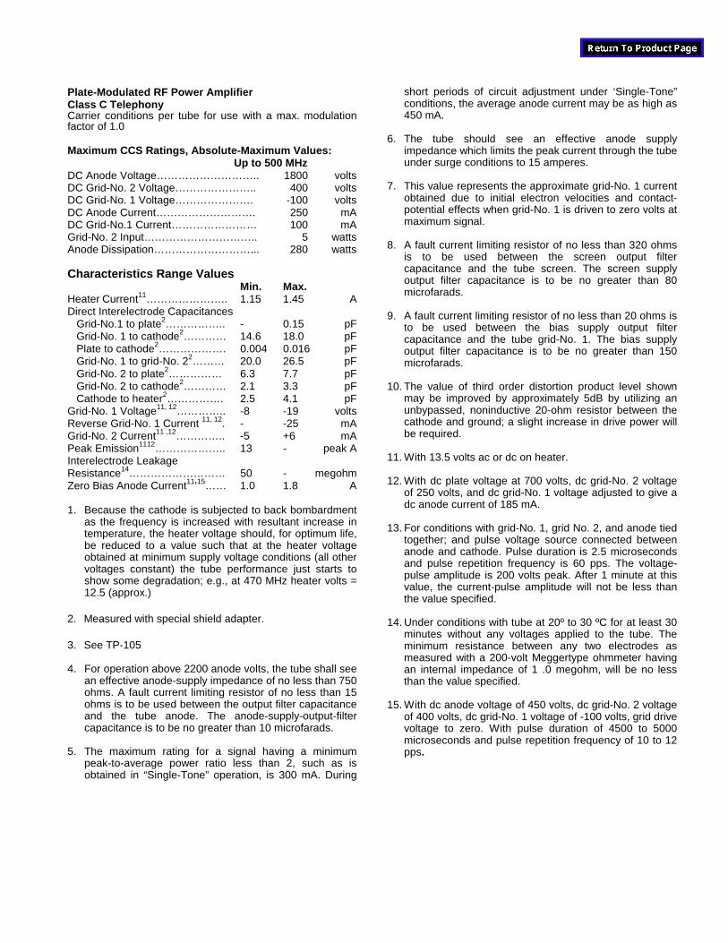
Plate-Modulated RF Power AmplifierClass C TelephonyCarrier conditions per tube for use with a max. modulationfactor of 1.0
Maximum CCS Ratings, Absolute-Maximum Values:Up to 500 MHz
DC Anode Voltage……………………….. 1800 voltsDC Grid-No. 2 Voltage………………….. 400 voltsDC Grid-No. 1 Voltage…………………. -100 voltsDC Anode Current………………………. 250 mADC Grid-No.1 Current…………………… 100 mAGrid-No. 2 Input………………………….. 5 wattsAnode Dissipation………………………... 280 watts
Characteristics Range ValuesMin. Max.
Heater Current11………………….. 1.15 1.45 ADirect Interelectrode Capacitances
Grid-No.1 to plate2…………….. - 0.15 pFGrid-No. 1 to cathode2………… 14.6 18.0 pFPlate to cathode2………………. 0.004 0.016 pFGrid-No. 1 to grid-No. 22……… 20.0 26.5 pFGrid-No. 2 to plate2…………… 6.3 7.7 pFGrid-No. 2 to cathode2………… 2.1 3.3 pFCathode to heater2……………. 2.5 4.1 pF
Grid-No. 1 Voltage11, 12………….. -8 -19 voltsReverse Grid-No. 1 Current 11, 12. - -25 mAGrid-No. 2 Current11 ,12………….. -5 +6 mAPeak Emission1112……………….. 13 - peak AInterelectrode LeakageResistance14……………………… 50 - megohmZero Bias Anode Current11’15…… 1.0 1.8 A
1. Because the cathode is subjected to back bombardmentas the frequency is increased with resultant increase intemperature, the heater voltage should, for optimum life,be reduced to a value such that at the heater voltageobtained at minimum supply voltage conditions (all othervoltages constant) the tube performance just starts toshow some degradation; e.g., at 470 MHz heater volts =12.5 (approx.)
2. Measured with special shield adapter.
3. See TP-105
4. For operation above 2200 anode volts, the tube shall seean effective anode-supply impedance of no less than 750ohms. A fault current limiting resistor of no less than 15ohms is to be used between the output filter capacitanceand the tube anode. The anode-supply-output-filtercapacitance is to be no greater than 10 microfarads.
5. The maximum rating for a signal having a minimumpeak-to-average power ratio less than 2, such as isobtained in “Single-Tone” operation, is 300 mA. During
short periods of circuit adjustment under ‘Single-Tone”conditions, the average anode current may be as high as450 mA.
6. The tube should see an effective anode supplyimpedance which limits the peak current through the tubeunder surge conditions to 15 amperes.
7. This value represents the approximate grid-No. 1 currentobtained due to initial electron velocities and contact-potential effects when grid-No. 1 is driven to zero volts atmaximum signal.
8. A fault current limiting resistor of no less than 320 ohmsis to be used between the screen output filtercapacitance and the tube screen. The screen supplyoutput filter capacitance is to be no greater than 80microfarads.
9. A fault current limiting resistor of no less than 20 ohms isto be used between the bias supply output filtercapacitance and the tube grid-No. 1. The bias supplyoutput filter capacitance is to be no greater than 150microfarads.
10. The value of third order distortion product level shownmay be improved by approximately 5dB by utilizing anunbypassed, noninductive 20-ohm resistor between thecathode and ground; a slight increase in drive power willbe required.
11. With 13.5 volts ac or dc on heater.
12. With dc plate voltage at 700 volts, dc grid-No. 2 voltageof 250 volts, and dc grid-No. 1 voltage adjusted to give adc anode current of 185 mA.
13. For conditions with grid-No. 1, grid No. 2, and anode tiedtogether; and pulse voltage source connected betweenanode and cathode. Pulse duration is 2.5 microsecondsand pulse repetition frequency is 60 pps. The voltage-pulse amplitude is 200 volts peak. After 1 minute at thisvalue, the current-pulse amplitude will not be less thanthe value specified.
14. Under conditions with tube at 20º to 30 ºC for at least 30minutes without any voltages applied to the tube. Theminimum resistance between any two electrodes asmeasured with a 200-volt Meggertype ohmmeter havingan internal impedance of 1 .0 megohm, will be no lessthan the value specified.
15. With dc anode voltage of 450 volts, dc grid-No. 2 voltageof 400 volts, dc grid-No. 1 voltage of -100 volts, grid drivevoltage to zero. With pulse duration of 4500 to 5000microseconds and pulse repetition frequency of 10 to 12pps.
Operating Considerations for Type 8122/V1-Matched PairFollow all of the recommendations and instructions outlinedby the equipment manufacturers with special emphasis onthe following precautions:
1. Always allow at least three minutes for the tube heatersto warm up before any other voltages are applied orbefore any current is drawn.
2. During CW tune-up procedure, the total screen currentfor both tubes should never exceed 15 milliamperes.
3. During CW tune-up procedure the total anode current forboth tubes should never exceed 550 milliamperes.
4. In the SSB mode, the total anode current for both tubesshould not exceed 400 milliamperes during voice peaks.A sustained tone like a whistle should not be permitted.
5. Check the socket wiring to assure that each of the threepins provided for the cathode, grid and screen electrodesare interconnected rather than using one pin for eachelectrode. (See basing diagram of tube bulletin.)
6. Use only 8122/V1 for “matched pair” performance.
If an unmatched pair is used in a parallel circuit nothaving individual bias adjustment for each tube, one tubewill carry most of the load current and, consequently, willbe operated out of ratings.
7. Never rap a tube or equipment. Each tube of the8122/V1 set has closely spaced electrodes which controlthe tube’s electrical characteristics. Bumping or rappingthe tubes or the equipment may change the spacings,thereby destroying the matched characteristics of thetubes.
8. The operating voltages applied to these devices presentsan electrical shock hazard. The tubes and associatedapparatus should be housed in a protective enclosure tokeep all personnel from coming in contact with highvoltage. The protective enclosure should be designedwith interlocks to break the primary circuit of the high-voltage supplies, discharging high-voltage capacitorswhen any door or gate on the protective housing isopened, and should prevent the closing of the primarycircuit until the door or gate is again closed.
9. DO NOT use the remaining tube of a matched pair withany other remaining or new tube. The tubes will beunbalanced and will fail prematurely.
References1. Application Guide for BURLE Power Tubes, TP-105.2. Screen-Grid Current Loading and Bleeder
Considerations, TP-1223. Application Guide for Forced Air Cooling of BURLE
Power Tubes TP-118
Figure 1 – Typical Cooling Requirements

Figure 2 - Typical Constant-Current Characteristics For Grid-No. 2 Voltage = 400 Volts
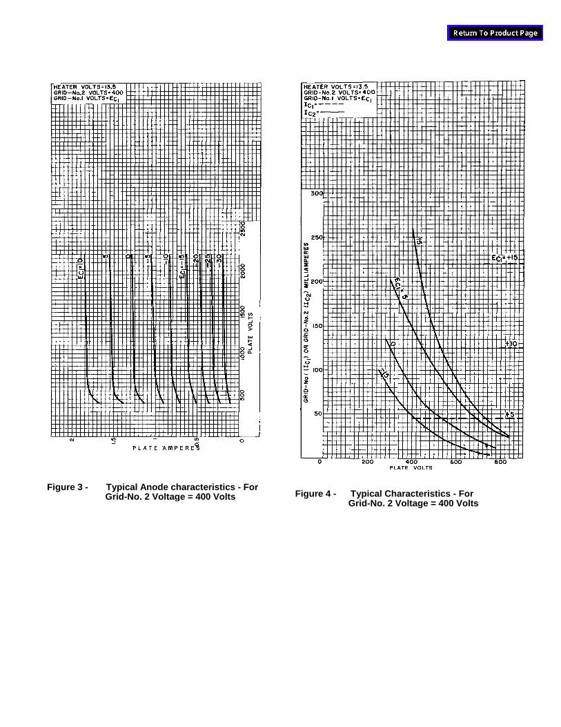
Figure 4 - Typical Characteristics - ForGrid-No. 2 Voltage = 400 Volts
Figure 3 - Typical Anode characteristics - ForGrid-No. 2 Voltage = 400 Volts
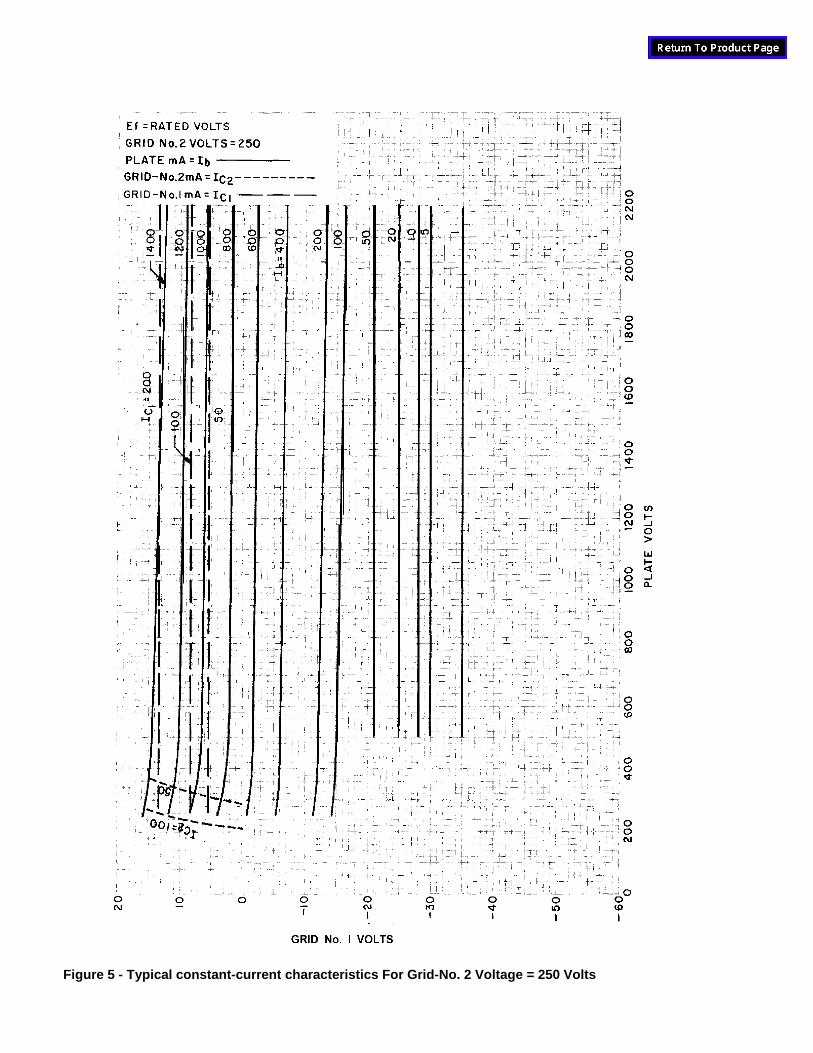
Figure 5 - Typical constant-current characteristics For Grid-No. 2 Voltage = 250 Volts

Note 1: Keep all stippled regions clear. Do not allow contacts or circuitcomponents to protrude into these annular volumes.
Note 2: The diameters of the radiator, grid-No. 2 terminal contactsurface, and pin circle to be concentric within the followingvalues of maximum full indicator reading:
Radiator to Grid-No. 2Terminal Contact Surface……………………… 0.030” max.Radiator to Pin Circle……………………………0.040” max.Grid-No. 2 Terminal ContactSurface to Pin Circle…………………………… 0.030” max.
Note 3: The full indicator reading is the maximum deviation in radial
position of a surface when the tube is completely rotated aboutthe center of the reference surface. It is a measure of the totaleffect of run-out and ellipticity.
Figure 6 - Dimensional Outline
Pin1: Cathode Pin 9: CathodePin2: Grid-No.2 Pin 10: Grid-No.2Pin3: Grid-No.1 Pin 11: Grid-No.1Pin4: Cathode Cap: Anode TerminalPin5: Heater Radiator: Anode TerminalPin6: Heater Ring: Grid-No. 2 Terminal ContactPin7: Grid-No.2 Surface (For use at higher frequen-Pin8: Grid-No.1 cies)
Figure 8 - Basing Diagram - Bottom View
Figure 9 - Gauge Drawing JEDEC No. GE11-1
* This dimension around the periphery of any individual pinmay vary within the limits shown.Figure 7 - Base Drawing Large-WaferElevenar 11-Pin With Ring JEDEC No. E11-81