Embed Size (px)
Citation preview
March 1994 Order Number: 290253-006
82357INTEGRATED SYSTEM PERIPHERAL (ISP)
Y Provides Enhanced DMA FunctionsÐ ISA/EISA DMA Compatible CyclesÐ All Transfers are Fly-By TransfersÐ 32-Bit AddressabilityÐ Seven Independently Programmable
ChannelsÐ Provides Timing Control for 8-, 16-,
and 32-Bit DMA Data TransfersÐ Provides Timing Control for
Compatible, Type ‘‘A’’, Type ‘‘B’’, andType ‘‘C’’ (Burst) Cycle Types
Ð 33 Mbytes/sec Maximum DataTransfer Rate
Ð Provides Refresh AddressGeneration
Ð Supports Data CommunicationDevices and Other Devices ThatWork from a Ring Buffer in Memory
Ð Incorporates the Functionality ofTwo 82C37A DMA Controllers
Y Provides High Performance ArbitrationÐ For CPU, EISA/ISA Bus Masters,
DMA Channels, and Refresh
Y Incorporates the Functionality of Two82C59A Interrupt ControllersÐ 14 Independently Programmable
Channels for Level-or-EdgeTriggered Interrupts
Y Five Programmable 16-Bit Counter/TimersÐ Generates Refresh Request SignalÐ System Timer InterruptÐ Speaker Tone OutputÐ Fail-Safe TimerÐ Periodic CPU Speed ControlÐ 82C54 Programmable Interval Timer
Compatible
Y Provides Logic for Generation/Controlof Non-Maskable InterruptsÐ Parity Errors for System and
Expansion Board MemoryÐ 8 ms and 32 ms Bus TimeoutÐ Immediate NMI Interrupt via
Software ControlÐ Fail-Safe Timer
Y 132-Pin PQFP Package(See Packaging Specifications: Order Number 240800,Package Type NG)
82357 Internal Block Diagram
290253–78Intel486 is a trademark of Intel Corporation.
82357 Integrated System Peripheral (ISP)
CONTENTS PAGE
82357 INTEGRATED SYSTEM PERIPHERAL ÀÀÀÀÀÀÀÀÀÀÀÀÀÀÀÀÀÀÀÀÀÀÀÀÀÀÀÀÀÀÀÀÀÀÀÀÀÀÀÀÀÀÀÀÀÀÀ 1FUNCTIONAL HIGHLIGHTS ÀÀÀÀÀÀÀÀÀÀÀÀÀÀÀÀÀÀÀÀÀÀÀÀÀÀÀÀÀÀÀÀÀÀÀÀÀÀÀÀÀÀÀÀÀÀÀÀÀÀÀÀÀÀÀÀÀ 1
1.0 ISP SYSTEM INTERFACE ILLUSTRATION ÀÀÀÀÀÀÀÀÀÀÀÀÀÀÀÀÀÀÀÀÀÀÀÀÀÀÀÀÀÀÀÀÀÀÀÀÀÀÀÀÀÀÀÀÀÀÀ 7
2.0 FUNCTIONAL OVERVIEW ÀÀÀÀÀÀÀÀÀÀÀÀÀÀÀÀÀÀÀÀÀÀÀÀÀÀÀÀÀÀÀÀÀÀÀÀÀÀÀÀÀÀÀÀÀÀÀÀÀÀÀÀÀÀÀÀÀÀÀÀÀÀÀÀ 7
2.1 Master and Slave Modes ÀÀÀÀÀÀÀÀÀÀÀÀÀÀÀÀÀÀÀÀÀÀÀÀÀÀÀÀÀÀÀÀÀÀÀÀÀÀÀÀÀÀÀÀÀÀÀÀÀÀÀÀÀÀÀÀÀÀÀÀÀÀÀ 7
2.2 DMA Controller ÀÀÀÀÀÀÀÀÀÀÀÀÀÀÀÀÀÀÀÀÀÀÀÀÀÀÀÀÀÀÀÀÀÀÀÀÀÀÀÀÀÀÀÀÀÀÀÀÀÀÀÀÀÀÀÀÀÀÀÀÀÀÀÀÀÀÀÀÀÀÀÀÀ 7
2.3 System Arbiter ÀÀÀÀÀÀÀÀÀÀÀÀÀÀÀÀÀÀÀÀÀÀÀÀÀÀÀÀÀÀÀÀÀÀÀÀÀÀÀÀÀÀÀÀÀÀÀÀÀÀÀÀÀÀÀÀÀÀÀÀÀÀÀÀÀÀÀÀÀÀÀÀÀ 8
2.3.1 Priorities of Requesters ÀÀÀÀÀÀÀÀÀÀÀÀÀÀÀÀÀÀÀÀÀÀÀÀÀÀÀÀÀÀÀÀÀÀÀÀÀÀÀÀÀÀÀÀÀÀÀÀÀÀÀÀÀÀÀÀÀÀÀÀ 9
2.3.2 Preemption of EISA Masters and DMA Devices ÀÀÀÀÀÀÀÀÀÀÀÀÀÀÀÀÀÀÀÀÀÀÀÀÀÀÀÀÀÀÀÀÀÀÀÀÀ 9
2.3.3 Arbitration During Non-Maskable Interrupts ÀÀÀÀÀÀÀÀÀÀÀÀÀÀÀÀÀÀÀÀÀÀÀÀÀÀÀÀÀÀÀÀÀÀÀÀÀÀÀÀ 10
2.3.4 DREQ and DACK Latency Control ÀÀÀÀÀÀÀÀÀÀÀÀÀÀÀÀÀÀÀÀÀÀÀÀÀÀÀÀÀÀÀÀÀÀÀÀÀÀÀÀÀÀÀÀÀÀÀÀ 10
2.4 Refresh Generation ÀÀÀÀÀÀÀÀÀÀÀÀÀÀÀÀÀÀÀÀÀÀÀÀÀÀÀÀÀÀÀÀÀÀÀÀÀÀÀÀÀÀÀÀÀÀÀÀÀÀÀÀÀÀÀÀÀÀÀÀÀÀÀÀÀÀÀ 10
2.5 Interrupt Controller ÀÀÀÀÀÀÀÀÀÀÀÀÀÀÀÀÀÀÀÀÀÀÀÀÀÀÀÀÀÀÀÀÀÀÀÀÀÀÀÀÀÀÀÀÀÀÀÀÀÀÀÀÀÀÀÀÀÀÀÀÀÀÀÀÀÀÀÀ 11
2.6 Non-Maskable Interrupt (NMI) ÀÀÀÀÀÀÀÀÀÀÀÀÀÀÀÀÀÀÀÀÀÀÀÀÀÀÀÀÀÀÀÀÀÀÀÀÀÀÀÀÀÀÀÀÀÀÀÀÀÀÀÀÀÀÀÀÀ 12
2.7 Interval Timers ÀÀÀÀÀÀÀÀÀÀÀÀÀÀÀÀÀÀÀÀÀÀÀÀÀÀÀÀÀÀÀÀÀÀÀÀÀÀÀÀÀÀÀÀÀÀÀÀÀÀÀÀÀÀÀÀÀÀÀÀÀÀÀÀÀÀÀÀÀÀÀÀ 13
2.8 Register Access ÀÀÀÀÀÀÀÀÀÀÀÀÀÀÀÀÀÀÀÀÀÀÀÀÀÀÀÀÀÀÀÀÀÀÀÀÀÀÀÀÀÀÀÀÀÀÀÀÀÀÀÀÀÀÀÀÀÀÀÀÀÀÀÀÀÀÀÀÀÀÀ 14
3.0 DMA CONTROLLER ÀÀÀÀÀÀÀÀÀÀÀÀÀÀÀÀÀÀÀÀÀÀÀÀÀÀÀÀÀÀÀÀÀÀÀÀÀÀÀÀÀÀÀÀÀÀÀÀÀÀÀÀÀÀÀÀÀÀÀÀÀÀÀÀÀÀÀÀÀ 14
3.1 DMA Transfer Modes ÀÀÀÀÀÀÀÀÀÀÀÀÀÀÀÀÀÀÀÀÀÀÀÀÀÀÀÀÀÀÀÀÀÀÀÀÀÀÀÀÀÀÀÀÀÀÀÀÀÀÀÀÀÀÀÀÀÀÀÀÀÀÀÀÀÀ 14
3.1.1 Single Transfer Mode ÀÀÀÀÀÀÀÀÀÀÀÀÀÀÀÀÀÀÀÀÀÀÀÀÀÀÀÀÀÀÀÀÀÀÀÀÀÀÀÀÀÀÀÀÀÀÀÀÀÀÀÀÀÀÀÀÀÀÀÀÀ 14
3.1.2 Block Transfer Mode ÀÀÀÀÀÀÀÀÀÀÀÀÀÀÀÀÀÀÀÀÀÀÀÀÀÀÀÀÀÀÀÀÀÀÀÀÀÀÀÀÀÀÀÀÀÀÀÀÀÀÀÀÀÀÀÀÀÀÀÀÀ 15
3.1.3 Demand Transfer Mode ÀÀÀÀÀÀÀÀÀÀÀÀÀÀÀÀÀÀÀÀÀÀÀÀÀÀÀÀÀÀÀÀÀÀÀÀÀÀÀÀÀÀÀÀÀÀÀÀÀÀÀÀÀÀÀÀÀÀ 15
3.1.4 Cascade Mode ÀÀÀÀÀÀÀÀÀÀÀÀÀÀÀÀÀÀÀÀÀÀÀÀÀÀÀÀÀÀÀÀÀÀÀÀÀÀÀÀÀÀÀÀÀÀÀÀÀÀÀÀÀÀÀÀÀÀÀÀÀÀÀÀÀÀÀ 15
3.2 Transfer Types ÀÀÀÀÀÀÀÀÀÀÀÀÀÀÀÀÀÀÀÀÀÀÀÀÀÀÀÀÀÀÀÀÀÀÀÀÀÀÀÀÀÀÀÀÀÀÀÀÀÀÀÀÀÀÀÀÀÀÀÀÀÀÀÀÀÀÀÀÀÀÀÀ 15
3.2.1 Write Transfer ÀÀÀÀÀÀÀÀÀÀÀÀÀÀÀÀÀÀÀÀÀÀÀÀÀÀÀÀÀÀÀÀÀÀÀÀÀÀÀÀÀÀÀÀÀÀÀÀÀÀÀÀÀÀÀÀÀÀÀÀÀÀÀÀÀÀÀÀ 15
3.2.2 Read Transfer ÀÀÀÀÀÀÀÀÀÀÀÀÀÀÀÀÀÀÀÀÀÀÀÀÀÀÀÀÀÀÀÀÀÀÀÀÀÀÀÀÀÀÀÀÀÀÀÀÀÀÀÀÀÀÀÀÀÀÀÀÀÀÀÀÀÀÀÀ 15
3.2.3 Verify Transfer ÀÀÀÀÀÀÀÀÀÀÀÀÀÀÀÀÀÀÀÀÀÀÀÀÀÀÀÀÀÀÀÀÀÀÀÀÀÀÀÀÀÀÀÀÀÀÀÀÀÀÀÀÀÀÀÀÀÀÀÀÀÀÀÀÀÀÀÀ 15
3.3 Autoinitialize ÀÀÀÀÀÀÀÀÀÀÀÀÀÀÀÀÀÀÀÀÀÀÀÀÀÀÀÀÀÀÀÀÀÀÀÀÀÀÀÀÀÀÀÀÀÀÀÀÀÀÀÀÀÀÀÀÀÀÀÀÀÀÀÀÀÀÀÀÀÀÀÀÀÀ 15
3.4 Channel Priority ÀÀÀÀÀÀÀÀÀÀÀÀÀÀÀÀÀÀÀÀÀÀÀÀÀÀÀÀÀÀÀÀÀÀÀÀÀÀÀÀÀÀÀÀÀÀÀÀÀÀÀÀÀÀÀÀÀÀÀÀÀÀÀÀÀÀÀÀÀÀÀ 16
3.4.1 Fixed Priority ÀÀÀÀÀÀÀÀÀÀÀÀÀÀÀÀÀÀÀÀÀÀÀÀÀÀÀÀÀÀÀÀÀÀÀÀÀÀÀÀÀÀÀÀÀÀÀÀÀÀÀÀÀÀÀÀÀÀÀÀÀÀÀÀÀÀÀÀÀ 16
3.4.2 Rotating Priority ÀÀÀÀÀÀÀÀÀÀÀÀÀÀÀÀÀÀÀÀÀÀÀÀÀÀÀÀÀÀÀÀÀÀÀÀÀÀÀÀÀÀÀÀÀÀÀÀÀÀÀÀÀÀÀÀÀÀÀÀÀÀÀÀÀÀ 16
3.5 Buffer Chaining ÀÀÀÀÀÀÀÀÀÀÀÀÀÀÀÀÀÀÀÀÀÀÀÀÀÀÀÀÀÀÀÀÀÀÀÀÀÀÀÀÀÀÀÀÀÀÀÀÀÀÀÀÀÀÀÀÀÀÀÀÀÀÀÀÀÀÀÀÀÀÀÀ 16
3.6 DMA Enhanced Timing ÀÀÀÀÀÀÀÀÀÀÀÀÀÀÀÀÀÀÀÀÀÀÀÀÀÀÀÀÀÀÀÀÀÀÀÀÀÀÀÀÀÀÀÀÀÀÀÀÀÀÀÀÀÀÀÀÀÀÀÀÀÀÀÀ 18
3.6.1 Compatible Timing ÀÀÀÀÀÀÀÀÀÀÀÀÀÀÀÀÀÀÀÀÀÀÀÀÀÀÀÀÀÀÀÀÀÀÀÀÀÀÀÀÀÀÀÀÀÀÀÀÀÀÀÀÀÀÀÀÀÀÀÀÀÀÀÀ 18
3.6.2 Type ‘‘A’’ Timing ÀÀÀÀÀÀÀÀÀÀÀÀÀÀÀÀÀÀÀÀÀÀÀÀÀÀÀÀÀÀÀÀÀÀÀÀÀÀÀÀÀÀÀÀÀÀÀÀÀÀÀÀÀÀÀÀÀÀÀÀÀÀÀÀÀÀ 18
3.6.3 Type ‘‘B’’ Timing ÀÀÀÀÀÀÀÀÀÀÀÀÀÀÀÀÀÀÀÀÀÀÀÀÀÀÀÀÀÀÀÀÀÀÀÀÀÀÀÀÀÀÀÀÀÀÀÀÀÀÀÀÀÀÀÀÀÀÀÀÀÀÀÀÀÀ 18
3.6.4 Type ‘‘C’’ (Burst Timing) ÀÀÀÀÀÀÀÀÀÀÀÀÀÀÀÀÀÀÀÀÀÀÀÀÀÀÀÀÀÀÀÀÀÀÀÀÀÀÀÀÀÀÀÀÀÀÀÀÀÀÀÀÀÀÀÀÀÀ 18
2
82357
CONTENTS PAGE
3.7 Register Description ÀÀÀÀÀÀÀÀÀÀÀÀÀÀÀÀÀÀÀÀÀÀÀÀÀÀÀÀÀÀÀÀÀÀÀÀÀÀÀÀÀÀÀÀÀÀÀÀÀÀÀÀÀÀÀÀÀÀÀÀÀÀÀÀÀÀÀ 18
3.7.1 Stop Registers (Ring Buffer Data Structure) ÀÀÀÀÀÀÀÀÀÀÀÀÀÀÀÀÀÀÀÀÀÀÀÀÀÀÀÀÀÀÀÀÀÀÀÀÀÀÀ 18
3.7.2 DMA Memory Low Page Register ÀÀÀÀÀÀÀÀÀÀÀÀÀÀÀÀÀÀÀÀÀÀÀÀÀÀÀÀÀÀÀÀÀÀÀÀÀÀÀÀÀÀÀÀÀÀÀÀÀ 20
3.7.3 DMA Memory High Page Register ÀÀÀÀÀÀÀÀÀÀÀÀÀÀÀÀÀÀÀÀÀÀÀÀÀÀÀÀÀÀÀÀÀÀÀÀÀÀÀÀÀÀÀÀÀÀÀÀÀ 20
3.7.3.1 Address Compatibility Mode ÀÀÀÀÀÀÀÀÀÀÀÀÀÀÀÀÀÀÀÀÀÀÀÀÀÀÀÀÀÀÀÀÀÀÀÀÀÀÀÀÀÀÀÀÀÀÀÀÀ 21
3.7.4 Current Address Register (READ/WRITE) ÀÀÀÀÀÀÀÀÀÀÀÀÀÀÀÀÀÀÀÀÀÀÀÀÀÀÀÀÀÀÀÀÀÀÀÀÀÀÀÀ 21
3.7.4.1 Address Shifting when Programmed for
16-Bit I/O Count By Words ÀÀÀÀÀÀÀÀÀÀÀÀÀÀÀÀÀÀÀÀÀÀÀÀÀÀÀÀÀÀÀÀÀÀÀÀÀÀÀÀÀÀÀÀÀÀÀÀÀÀÀ 21
3.7.5 Current Word Register (READ/WRITE) ÀÀÀÀÀÀÀÀÀÀÀÀÀÀÀÀÀÀÀÀÀÀÀÀÀÀÀÀÀÀÀÀÀÀÀÀÀÀÀÀÀÀÀ 22
3.7.6 Base Page, Base Address and Base Word Count Registers ÀÀÀÀÀÀÀÀÀÀÀÀÀÀÀÀÀÀÀÀÀÀÀÀ 22
3.7.7 Command Register ÀÀÀÀÀÀÀÀÀÀÀÀÀÀÀÀÀÀÀÀÀÀÀÀÀÀÀÀÀÀÀÀÀÀÀÀÀÀÀÀÀÀÀÀÀÀÀÀÀÀÀÀÀÀÀÀÀÀÀÀÀÀÀ 22
3.7.8 Mode Register ÀÀÀÀÀÀÀÀÀÀÀÀÀÀÀÀÀÀÀÀÀÀÀÀÀÀÀÀÀÀÀÀÀÀÀÀÀÀÀÀÀÀÀÀÀÀÀÀÀÀÀÀÀÀÀÀÀÀÀÀÀÀÀÀÀÀÀÀ 23
3.7.9 Extended Mode Registers (WRITE ONLY) ÀÀÀÀÀÀÀÀÀÀÀÀÀÀÀÀÀÀÀÀÀÀÀÀÀÀÀÀÀÀÀÀÀÀÀÀÀÀÀÀ 23
3.7.9.1 8-Bit I/O, ‘‘Count By Bytes’’ Mode ÀÀÀÀÀÀÀÀÀÀÀÀÀÀÀÀÀÀÀÀÀÀÀÀÀÀÀÀÀÀÀÀÀÀÀÀÀÀÀÀÀÀÀÀ 24
3.7.9.2 16-Bit I/O, ‘‘Count By Words’’
(Address Shifted) Mode ÀÀÀÀÀÀÀÀÀÀÀÀÀÀÀÀÀÀÀÀÀÀÀÀÀÀÀÀÀÀÀÀÀÀÀÀÀÀÀÀÀÀÀÀÀÀÀÀÀÀÀÀÀÀ 24
3.7.9.3 16-Bit I/O, ‘‘Count By Bytes’’ Mode ÀÀÀÀÀÀÀÀÀÀÀÀÀÀÀÀÀÀÀÀÀÀÀÀÀÀÀÀÀÀÀÀÀÀÀÀÀÀÀÀÀÀ 24
3.7.9.4 32-Bit I/O ‘‘Count By Bytes’’ Mode ÀÀÀÀÀÀÀÀÀÀÀÀÀÀÀÀÀÀÀÀÀÀÀÀÀÀÀÀÀÀÀÀÀÀÀÀÀÀÀÀÀÀÀ 24
3.7.9.5 EOP Input/Output Selection ÀÀÀÀÀÀÀÀÀÀÀÀÀÀÀÀÀÀÀÀÀÀÀÀÀÀÀÀÀÀÀÀÀÀÀÀÀÀÀÀÀÀÀÀÀÀÀÀÀ 24
3.7.9.6 Stop Register Selection ÀÀÀÀÀÀÀÀÀÀÀÀÀÀÀÀÀÀÀÀÀÀÀÀÀÀÀÀÀÀÀÀÀÀÀÀÀÀÀÀÀÀÀÀÀÀÀÀÀÀÀÀÀÀ 24
3.7.9.7 Summary of the DMA Transfer Sizes ÀÀÀÀÀÀÀÀÀÀÀÀÀÀÀÀÀÀÀÀÀÀÀÀÀÀÀÀÀÀÀÀÀÀÀÀÀÀÀÀÀ 24
3.7.10 Request Register (Write Only) ÀÀÀÀÀÀÀÀÀÀÀÀÀÀÀÀÀÀÀÀÀÀÀÀÀÀÀÀÀÀÀÀÀÀÀÀÀÀÀÀÀÀÀÀÀÀÀÀÀÀÀ 25
3.7.11 Mask Register ÀÀÀÀÀÀÀÀÀÀÀÀÀÀÀÀÀÀÀÀÀÀÀÀÀÀÀÀÀÀÀÀÀÀÀÀÀÀÀÀÀÀÀÀÀÀÀÀÀÀÀÀÀÀÀÀÀÀÀÀÀÀÀÀÀÀÀ 25
3.7.12 Status Register ÀÀÀÀÀÀÀÀÀÀÀÀÀÀÀÀÀÀÀÀÀÀÀÀÀÀÀÀÀÀÀÀÀÀÀÀÀÀÀÀÀÀÀÀÀÀÀÀÀÀÀÀÀÀÀÀÀÀÀÀÀÀÀÀÀÀ 26
3.7.13 Set Chaining Mode Register ÀÀÀÀÀÀÀÀÀÀÀÀÀÀÀÀÀÀÀÀÀÀÀÀÀÀÀÀÀÀÀÀÀÀÀÀÀÀÀÀÀÀÀÀÀÀÀÀÀÀÀÀÀ 27
3.7.14 Set Chaining Mode Status Register ÀÀÀÀÀÀÀÀÀÀÀÀÀÀÀÀÀÀÀÀÀÀÀÀÀÀÀÀÀÀÀÀÀÀÀÀÀÀÀÀÀÀÀÀÀÀ 28
3.7.15 Channel Interrupt Status Register ÀÀÀÀÀÀÀÀÀÀÀÀÀÀÀÀÀÀÀÀÀÀÀÀÀÀÀÀÀÀÀÀÀÀÀÀÀÀÀÀÀÀÀÀÀÀÀÀ 28
3.7.16 Chain Buffer Expiration Control Register ÀÀÀÀÀÀÀÀÀÀÀÀÀÀÀÀÀÀÀÀÀÀÀÀÀÀÀÀÀÀÀÀÀÀÀÀÀÀÀÀÀ 29
3.8 Software Commands ÀÀÀÀÀÀÀÀÀÀÀÀÀÀÀÀÀÀÀÀÀÀÀÀÀÀÀÀÀÀÀÀÀÀÀÀÀÀÀÀÀÀÀÀÀÀÀÀÀÀÀÀÀÀÀÀÀÀÀÀÀÀÀÀÀÀ 29
3.8.1 Clear Byte Pointer Flip-Flop ÀÀÀÀÀÀÀÀÀÀÀÀÀÀÀÀÀÀÀÀÀÀÀÀÀÀÀÀÀÀÀÀÀÀÀÀÀÀÀÀÀÀÀÀÀÀÀÀÀÀÀÀÀÀÀ 29
3.8.2 Master Clear ÀÀÀÀÀÀÀÀÀÀÀÀÀÀÀÀÀÀÀÀÀÀÀÀÀÀÀÀÀÀÀÀÀÀÀÀÀÀÀÀÀÀÀÀÀÀÀÀÀÀÀÀÀÀÀÀÀÀÀÀÀÀÀÀÀÀÀÀÀ 30
3.8.3 Clear Mask Register ÀÀÀÀÀÀÀÀÀÀÀÀÀÀÀÀÀÀÀÀÀÀÀÀÀÀÀÀÀÀÀÀÀÀÀÀÀÀÀÀÀÀÀÀÀÀÀÀÀÀÀÀÀÀÀÀÀÀÀÀÀÀ 30
3.9 Terminal Count/EOP Summary ÀÀÀÀÀÀÀÀÀÀÀÀÀÀÀÀÀÀÀÀÀÀÀÀÀÀÀÀÀÀÀÀÀÀÀÀÀÀÀÀÀÀÀÀÀÀÀÀÀÀÀÀÀÀÀÀ 30
4.0 BUS ARBITRATION ÀÀÀÀÀÀÀÀÀÀÀÀÀÀÀÀÀÀÀÀÀÀÀÀÀÀÀÀÀÀÀÀÀÀÀÀÀÀÀÀÀÀÀÀÀÀÀÀÀÀÀÀÀÀÀÀÀÀÀÀÀÀÀÀÀÀÀÀÀ 31
4.1 Bus Timeout ÀÀÀÀÀÀÀÀÀÀÀÀÀÀÀÀÀÀÀÀÀÀÀÀÀÀÀÀÀÀÀÀÀÀÀÀÀÀÀÀÀÀÀÀÀÀÀÀÀÀÀÀÀÀÀÀÀÀÀÀÀÀÀÀÀÀÀÀÀÀÀÀÀÀÀ 31
4.1.1 8 ms Bus Timeout ÀÀÀÀÀÀÀÀÀÀÀÀÀÀÀÀÀÀÀÀÀÀÀÀÀÀÀÀÀÀÀÀÀÀÀÀÀÀÀÀÀÀÀÀÀÀÀÀÀÀÀÀÀÀÀÀÀÀÀÀÀÀÀÀÀ 31
4.1.2 32 ms Bus Timeout ÀÀÀÀÀÀÀÀÀÀÀÀÀÀÀÀÀÀÀÀÀÀÀÀÀÀÀÀÀÀÀÀÀÀÀÀÀÀÀÀÀÀÀÀÀÀÀÀÀÀÀÀÀÀÀÀÀÀÀÀÀÀÀ 31
4.2 4 ms Limit on DMA Transfers ÀÀÀÀÀÀÀÀÀÀÀÀÀÀÀÀÀÀÀÀÀÀÀÀÀÀÀÀÀÀÀÀÀÀÀÀÀÀÀÀÀÀÀÀÀÀÀÀÀÀÀÀÀÀÀÀÀÀ 31
4.3 EISA Bus Master Status Latch ÀÀÀÀÀÀÀÀÀÀÀÀÀÀÀÀÀÀÀÀÀÀÀÀÀÀÀÀÀÀÀÀÀÀÀÀÀÀÀÀÀÀÀÀÀÀÀÀÀÀÀÀÀÀÀÀÀ 32
3

82357
CONTENTS PAGE
5.0 INTERRUPT CONTROLLER ÀÀÀÀÀÀÀÀÀÀÀÀÀÀÀÀÀÀÀÀÀÀÀÀÀÀÀÀÀÀÀÀÀÀÀÀÀÀÀÀÀÀÀÀÀÀÀÀÀÀÀÀÀÀÀÀÀÀÀÀÀ 33
5.1 Interrupt Controller I/O Address Map ÀÀÀÀÀÀÀÀÀÀÀÀÀÀÀÀÀÀÀÀÀÀÀÀÀÀÀÀÀÀÀÀÀÀÀÀÀÀÀÀÀÀÀÀÀÀÀÀÀÀ 33
5.2 Interrupt Definition Table ÀÀÀÀÀÀÀÀÀÀÀÀÀÀÀÀÀÀÀÀÀÀÀÀÀÀÀÀÀÀÀÀÀÀÀÀÀÀÀÀÀÀÀÀÀÀÀÀÀÀÀÀÀÀÀÀÀÀÀÀÀÀ 34
5.3 Interrupt Request Register (IRR) and In-Service Register (ISR) ÀÀÀÀÀÀÀÀÀÀÀÀÀÀÀÀÀÀÀÀÀÀÀÀÀ 34
5.4 Priority Resolver ÀÀÀÀÀÀÀÀÀÀÀÀÀÀÀÀÀÀÀÀÀÀÀÀÀÀÀÀÀÀÀÀÀÀÀÀÀÀÀÀÀÀÀÀÀÀÀÀÀÀÀÀÀÀÀÀÀÀÀÀÀÀÀÀÀÀÀÀÀÀÀ 34
5.5 Interrupt Mask Register (IMR) ÀÀÀÀÀÀÀÀÀÀÀÀÀÀÀÀÀÀÀÀÀÀÀÀÀÀÀÀÀÀÀÀÀÀÀÀÀÀÀÀÀÀÀÀÀÀÀÀÀÀÀÀÀÀÀÀÀÀ 34
5.6 INT (Interrupt) ÀÀÀÀÀÀÀÀÀÀÀÀÀÀÀÀÀÀÀÀÀÀÀÀÀÀÀÀÀÀÀÀÀÀÀÀÀÀÀÀÀÀÀÀÀÀÀÀÀÀÀÀÀÀÀÀÀÀÀÀÀÀÀÀÀÀÀÀÀÀÀÀÀ 34
5.7 INTAÝ/(ST2Ý) (Interrupt Acknowledge) ÀÀÀÀÀÀÀÀÀÀÀÀÀÀÀÀÀÀÀÀÀÀÀÀÀÀÀÀÀÀÀÀÀÀÀÀÀÀÀÀÀÀÀÀÀÀÀ 34
5.8 Interrupt Sequence ÀÀÀÀÀÀÀÀÀÀÀÀÀÀÀÀÀÀÀÀÀÀÀÀÀÀÀÀÀÀÀÀÀÀÀÀÀÀÀÀÀÀÀÀÀÀÀÀÀÀÀÀÀÀÀÀÀÀÀÀÀÀÀÀÀÀÀÀ 35
5.9 80 x 86 Mode ÀÀÀÀÀÀÀÀÀÀÀÀÀÀÀÀÀÀÀÀÀÀÀÀÀÀÀÀÀÀÀÀÀÀÀÀÀÀÀÀÀÀÀÀÀÀÀÀÀÀÀÀÀÀÀÀÀÀÀÀÀÀÀÀÀÀÀÀÀÀÀÀÀÀ 35
5.10 Programming the Interrupt Controller ÀÀÀÀÀÀÀÀÀÀÀÀÀÀÀÀÀÀÀÀÀÀÀÀÀÀÀÀÀÀÀÀÀÀÀÀÀÀÀÀÀÀÀÀÀÀÀÀÀ 36
5.11 Initialization Command Words ÀÀÀÀÀÀÀÀÀÀÀÀÀÀÀÀÀÀÀÀÀÀÀÀÀÀÀÀÀÀÀÀÀÀÀÀÀÀÀÀÀÀÀÀÀÀÀÀÀÀÀÀÀÀÀÀ 37
5.11.1 Initialization Command Words 1 and 2 (ICW1, ICW2) ÀÀÀÀÀÀÀÀÀÀÀÀÀÀÀÀÀÀÀÀÀÀÀÀÀÀÀÀÀ 37
5.11.2 Initialization Command Word 3 (ICW3) ÀÀÀÀÀÀÀÀÀÀÀÀÀÀÀÀÀÀÀÀÀÀÀÀÀÀÀÀÀÀÀÀÀÀÀÀÀÀÀÀÀÀÀ 38
5.11.3 Initialization Command Word 4 (ICW4) ÀÀÀÀÀÀÀÀÀÀÀÀÀÀÀÀÀÀÀÀÀÀÀÀÀÀÀÀÀÀÀÀÀÀÀÀÀÀÀÀÀÀÀ 39
5.12 Operation Control Words (OCWS) ÀÀÀÀÀÀÀÀÀÀÀÀÀÀÀÀÀÀÀÀÀÀÀÀÀÀÀÀÀÀÀÀÀÀÀÀÀÀÀÀÀÀÀÀÀÀÀÀÀÀÀÀ 40
5.12.1 Operation Control Word 1 (OCW1)ÐRead/Write ÀÀÀÀÀÀÀÀÀÀÀÀÀÀÀÀÀÀÀÀÀÀÀÀÀÀÀÀÀÀÀÀÀ 40
5.12.2 Operation Control Word 2 (OCW2) ÀÀÀÀÀÀÀÀÀÀÀÀÀÀÀÀÀÀÀÀÀÀÀÀÀÀÀÀÀÀÀÀÀÀÀÀÀÀÀÀÀÀÀÀÀÀÀ 40
5.12.3 Operation Control Word 3 (OCW3) ÀÀÀÀÀÀÀÀÀÀÀÀÀÀÀÀÀÀÀÀÀÀÀÀÀÀÀÀÀÀÀÀÀÀÀÀÀÀÀÀÀÀÀÀÀÀÀ 41
5.13 End-Of-Interrupt Operation ÀÀÀÀÀÀÀÀÀÀÀÀÀÀÀÀÀÀÀÀÀÀÀÀÀÀÀÀÀÀÀÀÀÀÀÀÀÀÀÀÀÀÀÀÀÀÀÀÀÀÀÀÀÀÀÀÀÀÀ 42
5.13.1 End Of Interrupt (EOI) ÀÀÀÀÀÀÀÀÀÀÀÀÀÀÀÀÀÀÀÀÀÀÀÀÀÀÀÀÀÀÀÀÀÀÀÀÀÀÀÀÀÀÀÀÀÀÀÀÀÀÀÀÀÀÀÀÀÀÀ 42
5.13.2 Automatic End Of Interrupt (AEOI) Mode ÀÀÀÀÀÀÀÀÀÀÀÀÀÀÀÀÀÀÀÀÀÀÀÀÀÀÀÀÀÀÀÀÀÀÀÀÀÀÀÀÀ 42
5.14 Modes of Operation ÀÀÀÀÀÀÀÀÀÀÀÀÀÀÀÀÀÀÀÀÀÀÀÀÀÀÀÀÀÀÀÀÀÀÀÀÀÀÀÀÀÀÀÀÀÀÀÀÀÀÀÀÀÀÀÀÀÀÀÀÀÀÀÀÀÀ 42
5.14.1 Fully Nested Mode ÀÀÀÀÀÀÀÀÀÀÀÀÀÀÀÀÀÀÀÀÀÀÀÀÀÀÀÀÀÀÀÀÀÀÀÀÀÀÀÀÀÀÀÀÀÀÀÀÀÀÀÀÀÀÀÀÀÀÀÀÀÀ 42
5.14.2 The Special Fully Nested Mode ÀÀÀÀÀÀÀÀÀÀÀÀÀÀÀÀÀÀÀÀÀÀÀÀÀÀÀÀÀÀÀÀÀÀÀÀÀÀÀÀÀÀÀÀÀÀÀÀÀÀ 42
5.14.3 Automatic Rotation (Equal Priority Devices) ÀÀÀÀÀÀÀÀÀÀÀÀÀÀÀÀÀÀÀÀÀÀÀÀÀÀÀÀÀÀÀÀÀÀÀÀÀÀ 43
5.14.4 Specific Rotation (Specific Priority) ÀÀÀÀÀÀÀÀÀÀÀÀÀÀÀÀÀÀÀÀÀÀÀÀÀÀÀÀÀÀÀÀÀÀÀÀÀÀÀÀÀÀÀÀÀÀÀ 43
5.14.5 Poll Command ÀÀÀÀÀÀÀÀÀÀÀÀÀÀÀÀÀÀÀÀÀÀÀÀÀÀÀÀÀÀÀÀÀÀÀÀÀÀÀÀÀÀÀÀÀÀÀÀÀÀÀÀÀÀÀÀÀÀÀÀÀÀÀÀÀÀ 43
5.14.6 Cascade Mode ÀÀÀÀÀÀÀÀÀÀÀÀÀÀÀÀÀÀÀÀÀÀÀÀÀÀÀÀÀÀÀÀÀÀÀÀÀÀÀÀÀÀÀÀÀÀÀÀÀÀÀÀÀÀÀÀÀÀÀÀÀÀÀÀÀÀ 44
5.14.7 Edge and Level Triggered Modes ÀÀÀÀÀÀÀÀÀÀÀÀÀÀÀÀÀÀÀÀÀÀÀÀÀÀÀÀÀÀÀÀÀÀÀÀÀÀÀÀÀÀÀÀÀÀÀÀ 44
5.14.7.1 Edge/Level Triggered Control Register (ELCR) ÀÀÀÀÀÀÀÀÀÀÀÀÀÀÀÀÀÀÀÀÀÀÀÀÀÀÀÀÀ 44
5.15 Interrupt Masks ÀÀÀÀÀÀÀÀÀÀÀÀÀÀÀÀÀÀÀÀÀÀÀÀÀÀÀÀÀÀÀÀÀÀÀÀÀÀÀÀÀÀÀÀÀÀÀÀÀÀÀÀÀÀÀÀÀÀÀÀÀÀÀÀÀÀÀÀÀÀ 45
5.15.1 Masking on an Individual Interrupt Request Basis ÀÀÀÀÀÀÀÀÀÀÀÀÀÀÀÀÀÀÀÀÀÀÀÀÀÀÀÀÀÀÀÀ 45
5.15.2 Special Mask Mode ÀÀÀÀÀÀÀÀÀÀÀÀÀÀÀÀÀÀÀÀÀÀÀÀÀÀÀÀÀÀÀÀÀÀÀÀÀÀÀÀÀÀÀÀÀÀÀÀÀÀÀÀÀÀÀÀÀÀÀÀÀ 45
5.16 Reading the Interrupt Controller Status ÀÀÀÀÀÀÀÀÀÀÀÀÀÀÀÀÀÀÀÀÀÀÀÀÀÀÀÀÀÀÀÀÀÀÀÀÀÀÀÀÀÀÀÀÀÀÀ 45
4
82357
CONTENTS PAGE
6.0 NON-MASKABLE INTERRUPT PORTS ÀÀÀÀÀÀÀÀÀÀÀÀÀÀÀÀÀÀÀÀÀÀÀÀÀÀÀÀÀÀÀÀÀÀÀÀÀÀÀÀÀÀÀÀÀÀÀÀÀÀ 46
6.1 NMI Status and Control (Port 061h) ÀÀÀÀÀÀÀÀÀÀÀÀÀÀÀÀÀÀÀÀÀÀÀÀÀÀÀÀÀÀÀÀÀÀÀÀÀÀÀÀÀÀÀÀÀÀÀÀÀÀÀÀ 46
6.2 NMI Extended Status and Control (Port 0461h) ÀÀÀÀÀÀÀÀÀÀÀÀÀÀÀÀÀÀÀÀÀÀÀÀÀÀÀÀÀÀÀÀÀÀÀÀÀÀÀÀÀ 47
6.3 Software NMI Generation (Port 0462h) ÀÀÀÀÀÀÀÀÀÀÀÀÀÀÀÀÀÀÀÀÀÀÀÀÀÀÀÀÀÀÀÀÀÀÀÀÀÀÀÀÀÀÀÀÀÀÀÀÀ 48
6.4 NMI Enable/Disable and Real-Time Clock Address (Port 070h) ÀÀÀÀÀÀÀÀÀÀÀÀÀÀÀÀÀÀÀÀÀÀÀÀÀ 48
7.0 INTERVAL TIMER ÀÀÀÀÀÀÀÀÀÀÀÀÀÀÀÀÀÀÀÀÀÀÀÀÀÀÀÀÀÀÀÀÀÀÀÀÀÀÀÀÀÀÀÀÀÀÀÀÀÀÀÀÀÀÀÀÀÀÀÀÀÀÀÀÀÀÀÀÀÀÀ 48
7.1 Programming the Interval Timer ÀÀÀÀÀÀÀÀÀÀÀÀÀÀÀÀÀÀÀÀÀÀÀÀÀÀÀÀÀÀÀÀÀÀÀÀÀÀÀÀÀÀÀÀÀÀÀÀÀÀÀÀÀÀÀÀ 48
7.1.1 Interval Timer Control Word Format ÀÀÀÀÀÀÀÀÀÀÀÀÀÀÀÀÀÀÀÀÀÀÀÀÀÀÀÀÀÀÀÀÀÀÀÀÀÀÀÀÀÀÀÀÀÀÀ 49
7.1.2 Interval Timer Control Latch Command ÀÀÀÀÀÀÀÀÀÀÀÀÀÀÀÀÀÀÀÀÀÀÀÀÀÀÀÀÀÀÀÀÀÀÀÀÀÀÀÀÀÀÀÀ 49
7.1.3 Interval Timer Read Back Command ÀÀÀÀÀÀÀÀÀÀÀÀÀÀÀÀÀÀÀÀÀÀÀÀÀÀÀÀÀÀÀÀÀÀÀÀÀÀÀÀÀÀÀÀÀÀ 50
8.0 DETAILED SIGNAL DESCRIPTION ÀÀÀÀÀÀÀÀÀÀÀÀÀÀÀÀÀÀÀÀÀÀÀÀÀÀÀÀÀÀÀÀÀÀÀÀÀÀÀÀÀÀÀÀÀÀÀÀÀÀÀÀÀÀ 51
8.1 Signals Used during Arbitration ÀÀÀÀÀÀÀÀÀÀÀÀÀÀÀÀÀÀÀÀÀÀÀÀÀÀÀÀÀÀÀÀÀÀÀÀÀÀÀÀÀÀÀÀÀÀÀÀÀÀÀÀÀÀÀÀ 51
8.2 Signals Used during DMA and Register Access ÀÀÀÀÀÀÀÀÀÀÀÀÀÀÀÀÀÀÀÀÀÀÀÀÀÀÀÀÀÀÀÀÀÀÀÀÀÀÀÀ 53
8.3 Signals Used during an Interrupt Sequence ÀÀÀÀÀÀÀÀÀÀÀÀÀÀÀÀÀÀÀÀÀÀÀÀÀÀÀÀÀÀÀÀÀÀÀÀÀÀÀÀÀÀÀÀ 57
8.4 Counter/Timer, NMI and Miscellaneous Utility Signals ÀÀÀÀÀÀÀÀÀÀÀÀÀÀÀÀÀÀÀÀÀÀÀÀÀÀÀÀÀÀÀÀÀÀ 57
9.0 BASIC FUNCTION TIMING DIAGRAMS ÀÀÀÀÀÀÀÀÀÀÀÀÀÀÀÀÀÀÀÀÀÀÀÀÀÀÀÀÀÀÀÀÀÀÀÀÀÀÀÀÀÀÀÀÀÀÀÀÀ 59
9.1 Slave Mode ÀÀÀÀÀÀÀÀÀÀÀÀÀÀÀÀÀÀÀÀÀÀÀÀÀÀÀÀÀÀÀÀÀÀÀÀÀÀÀÀÀÀÀÀÀÀÀÀÀÀÀÀÀÀÀÀÀÀÀÀÀÀÀÀÀÀÀÀÀÀÀÀÀÀÀ 59
9.1.1 EISA Master or Host CPU Cycle to/from ISP ÀÀÀÀÀÀÀÀÀÀÀÀÀÀÀÀÀÀÀÀÀÀÀÀÀÀÀÀÀÀÀÀÀÀÀÀÀÀ 59
9.1.2 ISA Master Slave Cycle to/from the ISPÐShort Cycle ÀÀÀÀÀÀÀÀÀÀÀÀÀÀÀÀÀÀÀÀÀÀÀÀÀÀÀÀÀ 60
9.1.3 ISA Master Slave Cycle to/from the ISPÐLong Cycle ÀÀÀÀÀÀÀÀÀÀÀÀÀÀÀÀÀÀÀÀÀÀÀÀÀÀÀÀÀ 61
9.2 DMA Master Mode ÀÀÀÀÀÀÀÀÀÀÀÀÀÀÀÀÀÀÀÀÀÀÀÀÀÀÀÀÀÀÀÀÀÀÀÀÀÀÀÀÀÀÀÀÀÀÀÀÀÀÀÀÀÀÀÀÀÀÀÀÀÀÀÀÀÀÀÀ 62
9.2.1 Non-Burst DMA Cycles ÀÀÀÀÀÀÀÀÀÀÀÀÀÀÀÀÀÀÀÀÀÀÀÀÀÀÀÀÀÀÀÀÀÀÀÀÀÀÀÀÀÀÀÀÀÀÀÀÀÀÀÀÀÀÀÀÀÀÀ 62
9.2.2 Burst DMA Cycle Diagram 1 ÀÀÀÀÀÀÀÀÀÀÀÀÀÀÀÀÀÀÀÀÀÀÀÀÀÀÀÀÀÀÀÀÀÀÀÀÀÀÀÀÀÀÀÀÀÀÀÀÀÀÀÀÀÀ 63
9.2.3 Burst DMA Cycle Diagram 2 ÀÀÀÀÀÀÀÀÀÀÀÀÀÀÀÀÀÀÀÀÀÀÀÀÀÀÀÀÀÀÀÀÀÀÀÀÀÀÀÀÀÀÀÀÀÀÀÀÀÀÀÀÀÀ 64
9.2.4 Burst DMA Cycle Diagram 3 ÀÀÀÀÀÀÀÀÀÀÀÀÀÀÀÀÀÀÀÀÀÀÀÀÀÀÀÀÀÀÀÀÀÀÀÀÀÀÀÀÀÀÀÀÀÀÀÀÀÀÀÀÀÀ 65
9.2.5 EISA Refresh Cycle ÀÀÀÀÀÀÀÀÀÀÀÀÀÀÀÀÀÀÀÀÀÀÀÀÀÀÀÀÀÀÀÀÀÀÀÀÀÀÀÀÀÀÀÀÀÀÀÀÀÀÀÀÀÀÀÀÀÀÀÀÀÀÀ 65
9.3 Arbiter Timing Diagrams ÀÀÀÀÀÀÀÀÀÀÀÀÀÀÀÀÀÀÀÀÀÀÀÀÀÀÀÀÀÀÀÀÀÀÀÀÀÀÀÀÀÀÀÀÀÀÀÀÀÀÀÀÀÀÀÀÀÀÀÀÀÀÀ 66
9.3.1 Arbiter Timing Diagram 1 ÀÀÀÀÀÀÀÀÀÀÀÀÀÀÀÀÀÀÀÀÀÀÀÀÀÀÀÀÀÀÀÀÀÀÀÀÀÀÀÀÀÀÀÀÀÀÀÀÀÀÀÀÀÀÀÀÀÀ 66
9.3.2 Arbiter Timing Diagram 2 ÀÀÀÀÀÀÀÀÀÀÀÀÀÀÀÀÀÀÀÀÀÀÀÀÀÀÀÀÀÀÀÀÀÀÀÀÀÀÀÀÀÀÀÀÀÀÀÀÀÀÀÀÀÀÀÀÀÀ 67
9.3.3 Arbiter Timing Diagram 3 ÀÀÀÀÀÀÀÀÀÀÀÀÀÀÀÀÀÀÀÀÀÀÀÀÀÀÀÀÀÀÀÀÀÀÀÀÀÀÀÀÀÀÀÀÀÀÀÀÀÀÀÀÀÀÀÀÀÀ 68
9.3.4 Arbiter Timing Diagram 4 ÀÀÀÀÀÀÀÀÀÀÀÀÀÀÀÀÀÀÀÀÀÀÀÀÀÀÀÀÀÀÀÀÀÀÀÀÀÀÀÀÀÀÀÀÀÀÀÀÀÀÀÀÀÀÀÀÀÀ 69
9.3.5 Arbiter Timing Diagram 5 ÀÀÀÀÀÀÀÀÀÀÀÀÀÀÀÀÀÀÀÀÀÀÀÀÀÀÀÀÀÀÀÀÀÀÀÀÀÀÀÀÀÀÀÀÀÀÀÀÀÀÀÀÀÀÀÀÀÀ 70
9.3.6 Arbiter Timing Diagram 6ÐCIPÝ (ST3Ý) Timing ÀÀÀÀÀÀÀÀÀÀÀÀÀÀÀÀÀÀÀÀÀÀÀÀÀÀÀÀÀÀÀÀÀÀ 71
10.0 D.C. SPECIFICATIONS ÀÀÀÀÀÀÀÀÀÀÀÀÀÀÀÀÀÀÀÀÀÀÀÀÀÀÀÀÀÀÀÀÀÀÀÀÀÀÀÀÀÀÀÀÀÀÀÀÀÀÀÀÀÀÀÀÀÀÀÀÀÀÀÀÀ 72
10.1 Maximum Ratings ÀÀÀÀÀÀÀÀÀÀÀÀÀÀÀÀÀÀÀÀÀÀÀÀÀÀÀÀÀÀÀÀÀÀÀÀÀÀÀÀÀÀÀÀÀÀÀÀÀÀÀÀÀÀÀÀÀÀÀÀÀÀÀÀÀÀÀÀ 72
10.2 D.C. Specification Tables ÀÀÀÀÀÀÀÀÀÀÀÀÀÀÀÀÀÀÀÀÀÀÀÀÀÀÀÀÀÀÀÀÀÀÀÀÀÀÀÀÀÀÀÀÀÀÀÀÀÀÀÀÀÀÀÀÀÀÀÀÀ 72
5
82357
CONTENTS PAGE
11.0 A.C. SPECIFICATIONS ÀÀÀÀÀÀÀÀÀÀÀÀÀÀÀÀÀÀÀÀÀÀÀÀÀÀÀÀÀÀÀÀÀÀÀÀÀÀÀÀÀÀÀÀÀÀÀÀÀÀÀÀÀÀÀÀÀÀÀÀÀÀÀÀÀ 73
11.1 A.C. Characterization Tables ÀÀÀÀÀÀÀÀÀÀÀÀÀÀÀÀÀÀÀÀÀÀÀÀÀÀÀÀÀÀÀÀÀÀÀÀÀÀÀÀÀÀÀÀÀÀÀÀÀÀÀÀÀÀÀÀÀ 73
11.2 A.C. Characteristic Waveforms ÀÀÀÀÀÀÀÀÀÀÀÀÀÀÀÀÀÀÀÀÀÀÀÀÀÀÀÀÀÀÀÀÀÀÀÀÀÀÀÀÀÀÀÀÀÀÀÀÀÀÀÀÀÀÀ 77
11.2.1 BCLK, OSC Timing ÀÀÀÀÀÀÀÀÀÀÀÀÀÀÀÀÀÀÀÀÀÀÀÀÀÀÀÀÀÀÀÀÀÀÀÀÀÀÀÀÀÀÀÀÀÀÀÀÀÀÀÀÀÀÀÀÀÀÀÀÀÀ 77
11.2.2 Slave Mode Timing ÀÀÀÀÀÀÀÀÀÀÀÀÀÀÀÀÀÀÀÀÀÀÀÀÀÀÀÀÀÀÀÀÀÀÀÀÀÀÀÀÀÀÀÀÀÀÀÀÀÀÀÀÀÀÀÀÀÀÀÀÀÀ 78
11.2.3 DMA Master Timing ÀÀÀÀÀÀÀÀÀÀÀÀÀÀÀÀÀÀÀÀÀÀÀÀÀÀÀÀÀÀÀÀÀÀÀÀÀÀÀÀÀÀÀÀÀÀÀÀÀÀÀÀÀÀÀÀÀÀÀÀÀ 79
11.2.4 Arbiter Timing ÀÀÀÀÀÀÀÀÀÀÀÀÀÀÀÀÀÀÀÀÀÀÀÀÀÀÀÀÀÀÀÀÀÀÀÀÀÀÀÀÀÀÀÀÀÀÀÀÀÀÀÀÀÀÀÀÀÀÀÀÀÀÀÀÀÀÀ 80
11.2.5 Refresh Timing ÀÀÀÀÀÀÀÀÀÀÀÀÀÀÀÀÀÀÀÀÀÀÀÀÀÀÀÀÀÀÀÀÀÀÀÀÀÀÀÀÀÀÀÀÀÀÀÀÀÀÀÀÀÀÀÀÀÀÀÀÀÀÀÀÀÀ 81
11.2.6 Reset Timing ÀÀÀÀÀÀÀÀÀÀÀÀÀÀÀÀÀÀÀÀÀÀÀÀÀÀÀÀÀÀÀÀÀÀÀÀÀÀÀÀÀÀÀÀÀÀÀÀÀÀÀÀÀÀÀÀÀÀÀÀÀÀÀÀÀÀÀÀ 81
11.2.7 NMI Timing ÀÀÀÀÀÀÀÀÀÀÀÀÀÀÀÀÀÀÀÀÀÀÀÀÀÀÀÀÀÀÀÀÀÀÀÀÀÀÀÀÀÀÀÀÀÀÀÀÀÀÀÀÀÀÀÀÀÀÀÀÀÀÀÀÀÀÀÀÀÀ 81
11.2.8 Interrupt Timing ÀÀÀÀÀÀÀÀÀÀÀÀÀÀÀÀÀÀÀÀÀÀÀÀÀÀÀÀÀÀÀÀÀÀÀÀÀÀÀÀÀÀÀÀÀÀÀÀÀÀÀÀÀÀÀÀÀÀÀÀÀÀÀÀÀ 82
11.2.9 Counter/Timer Timing ÀÀÀÀÀÀÀÀÀÀÀÀÀÀÀÀÀÀÀÀÀÀÀÀÀÀÀÀÀÀÀÀÀÀÀÀÀÀÀÀÀÀÀÀÀÀÀÀÀÀÀÀÀÀÀÀÀÀÀ 82
11.2.10 RTCALE, GT1MÝ Timing ÀÀÀÀÀÀÀÀÀÀÀÀÀÀÀÀÀÀÀÀÀÀÀÀÀÀÀÀÀÀÀÀÀÀÀÀÀÀÀÀÀÀÀÀÀÀÀÀÀÀÀÀÀÀ 82
12.0 ISP PIN AND PACKAGE INFORMATION ÀÀÀÀÀÀÀÀÀÀÀÀÀÀÀÀÀÀÀÀÀÀÀÀÀÀÀÀÀÀÀÀÀÀÀÀÀÀÀÀÀÀÀÀÀÀÀ 83
12.1 Signal Overview ÀÀÀÀÀÀÀÀÀÀÀÀÀÀÀÀÀÀÀÀÀÀÀÀÀÀÀÀÀÀÀÀÀÀÀÀÀÀÀÀÀÀÀÀÀÀÀÀÀÀÀÀÀÀÀÀÀÀÀÀÀÀÀÀÀÀÀÀÀÀ 83
12.2 132 Package ÀÀÀÀÀÀÀÀÀÀÀÀÀÀÀÀÀÀÀÀÀÀÀÀÀÀÀÀÀÀÀÀÀÀÀÀÀÀÀÀÀÀÀÀÀÀÀÀÀÀÀÀÀÀÀÀÀÀÀÀÀÀÀÀÀÀÀÀÀÀÀÀÀ 84
12.3 Device Pinout ÀÀÀÀÀÀÀÀÀÀÀÀÀÀÀÀÀÀÀÀÀÀÀÀÀÀÀÀÀÀÀÀÀÀÀÀÀÀÀÀÀÀÀÀÀÀÀÀÀÀÀÀÀÀÀÀÀÀÀÀÀÀÀÀÀÀÀÀÀÀÀÀ 85
13.0 ISP PORT ADDRESS / I/O DECODING ÀÀÀÀÀÀÀÀÀÀÀÀÀÀÀÀÀÀÀÀÀÀÀÀÀÀÀÀÀÀÀÀÀÀÀÀÀÀÀÀÀÀÀÀÀÀÀÀ 86
14.0 THERMAL SPECIFICATION ÀÀÀÀÀÀÀÀÀÀÀÀÀÀÀÀÀÀÀÀÀÀÀÀÀÀÀÀÀÀÀÀÀÀÀÀÀÀÀÀÀÀÀÀÀÀÀÀÀÀÀÀÀÀÀÀÀÀÀÀ 90
15.0 REVISION SUMMARY ÀÀÀÀÀÀÀÀÀÀÀÀÀÀÀÀÀÀÀÀÀÀÀÀÀÀÀÀÀÀÀÀÀÀÀÀÀÀÀÀÀÀÀÀÀÀÀÀÀÀÀÀÀÀÀÀÀÀÀÀÀÀÀÀÀÀ 91
6
82357
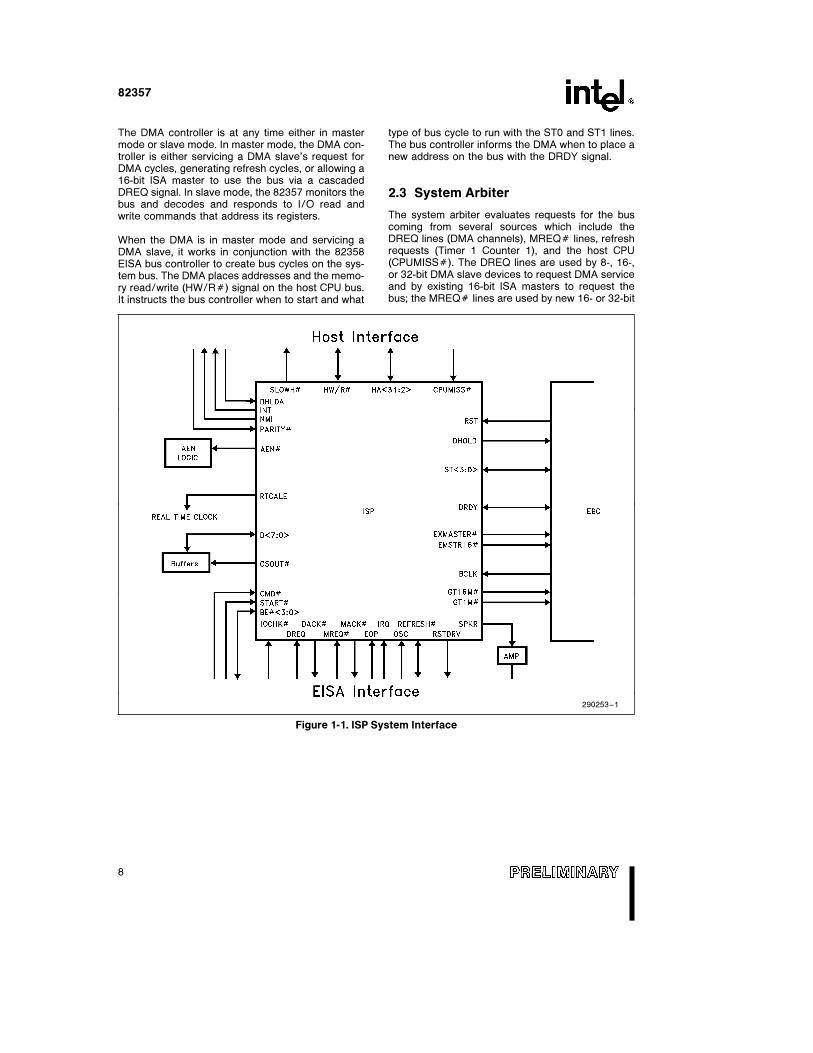
The 82357 is a multi-function support peripheral thatis designed to work in conjunction with the 82358 or82358DT EISA Bus Controller to provide most of thesystem functions necessary in EISA specific applica-tions.
The 82357 is comprised of several computer systemfunctions that are typically found in separate LSI andVLSI components. These include: a high perform-ance seven-channel programmable DMA Controller;an arbitration scheme that allows efficient bus shar-ing among multiple EISA masters, the host CPU, andDMA devices; a 16 level programmable interruptcontroller which provides level-or-edge triggered in-terrupt capability on a channel-by-channel basis;non-maskable interrupt logic for multiple NMI controland generation; refresh address generation andcontrol; and five counter/timers which provide a sys-tem timer interrupt, diskette time-out, DRAM refreshrequests, and other system timing operations.
The DMA controller on the 82357 provides the tim-ing control signals necessary to support a DMA datatransfer rate of 33 Mbytes/sec. The DMA controllerincludes full function 32-bit addressability with con-trol signal support for the transfer of data betweendevices of different data path widths using a singlechannel. Each channel functions independently inseveral modes.
1.0 ISP SYSTEM INTERFACEILLUSTRATION
The ISP connects to the Host bus, EISA bus, X busand EBC (Bus Controller). These connections areillustrated in Figure 1-1.
2.0 FUNCTIONAL OVERVIEW
The following is a brief discussion of the functionalityand features of the 82357. The DMA Controller, Ar-biter, Interrupt controller, NMI’s, and Timer/Coun-ters each have a corresponding detailed section lat-er in this data sheet.
2.1 Master and Slave Modes
The 82357 is either a slave device or a master de-vice.
In slave mode, the ISP monitors the address linesand decodes all bus cycles attempting to read orwrite any of its internal registers. In slave mode, ei-ther an EISA master or the host CPU can read orwrite to any of the ISP’s internal registers. 16-bit ISA
masters can read or write to any of the ISP’s 82C37PCAT compatible registers. The registers that can-not be accessed by an ISA master are located in theI/O space of 00H–0FH and 0C0H–ODFH. The ISPwill disable these registers upon granting the ISAmaster the bus. In slave mode, the ISP also detectsand responds to interrupt acknowledge cycles.
In master mode, the 82357 becomes the master ofthe bus system. It may peform either DMA cycles orrefresh cycles at this time.
The arbiter on the ISP determines which mode thedevice is in.
2.2 DMA Controller
The DMA circuitry incorporates the functionality oftwo 82C37 DMA controllers with seven indepen-dently programmable channels, (Channels 0–3 andChannels 5–7). DMA Channel 4 is used to cascadethe two controllers together and will default to cas-cade mode in the Mode register. In addition to ac-cepting requests from DMA slaves, the DMA alsoresponds to requests that are initiated by software.Software may initiate a DMA service request by set-ting any DMA channel Request register bit to a 1.
Any DMA channel may be programmed for 8-, 16-,or 32-bit DMA device size and ISA compatible, Type‘‘A’’, Type ‘‘B’’, or burst DMA Type ‘‘C’’ modes. The82357 provides the timing controls and the 82358EISA Bus Controller performs the data size transla-tions necessary for the DMA transfer. The DMAmemory addressing circuitry supports full 32-bit ad-dresses for DMA devices. Each channel includes a16-bit ISA compatible Current register which holdsthe 16 least-significant bits of the 32-bit address, aLow Page register which contains the eight secondmost significant bits, and a High Page register whichcontains the eight most significant bits of the 32-bitaddress.
The channels can also be programmed for any offour transfer modes. The transfer modes include sin-gle, block, demand, or cascade. Each of the threeactive transfer modes, (single, block, and demand),can perform three different types of transfers, (read,write, or verify). The DMA Controller also featuresrefresh address generation, buffer chaining, auto-ini-tialization, and support for a Ring Buffer Data Struc-ture in memory. Stop registers are used to help sup-port Data Communication or devices that work froma Ring Buffer in memory (refer to Section 3.7.1‘‘USE OF STOP REGISTERS’’).
7
82357
The DMA controller is at any time either in mastermode or slave mode. In master mode, the DMA con-troller is either servicing a DMA slave’s request forDMA cycles, generating refresh cycles, or allowing a16-bit ISA master to use the bus via a cascadedDREQ signal. In slave mode, the 82357 monitors thebus and decodes and responds to I/O read andwrite commands that address its registers.
When the DMA is in master mode and servicing aDMA slave, it works in conjunction with the 82358EISA bus controller to create bus cycles on the sys-tem bus. The DMA places addresses and the memo-ry read/write (HW/RÝ) signal on the host CPU bus.It instructs the bus controller when to start and what
type of bus cycle to run with the ST0 and ST1 lines.The bus controller informs the DMA when to place anew address on the bus with the DRDY signal.
2.3 System Arbiter
The system arbiter evaluates requests for the buscoming from several sources which include theDREQ lines (DMA channels), MREQÝ lines, refreshrequests (Timer 1 Counter 1), and the host CPU(CPUMISSÝ). The DREQ lines are used by 8-, 16-,or 32-bit DMA slave devices to request DMA serviceand by existing 16-bit ISA masters to request thebus; the MREQÝ lines are used by new 16- or 32-bit
290253–1
Figure 1-1. ISP System Interface
8
82357
EISA masters for general bus request; the CPUM-ISSÝ line is used by the host CPU when requestingbus access; and Timer 1 Counter 1 specifically isused to generate internal requests for refresh. Thedefault master of the bus is the CPU. It is grantedthe bus if there are no requesters.
The DMA channels, when used by 16-bit ISA mas-ters for direct access to the bus, must be placed inCascade mode. In Cascade mode, the DMA control-ler will respond to DREQ with DACKÝ andEMSTR16Ý, but HW/RÝ, ST0, ST1, Ak31:2l, andBEk3:0lÝ outputs will be disabled.
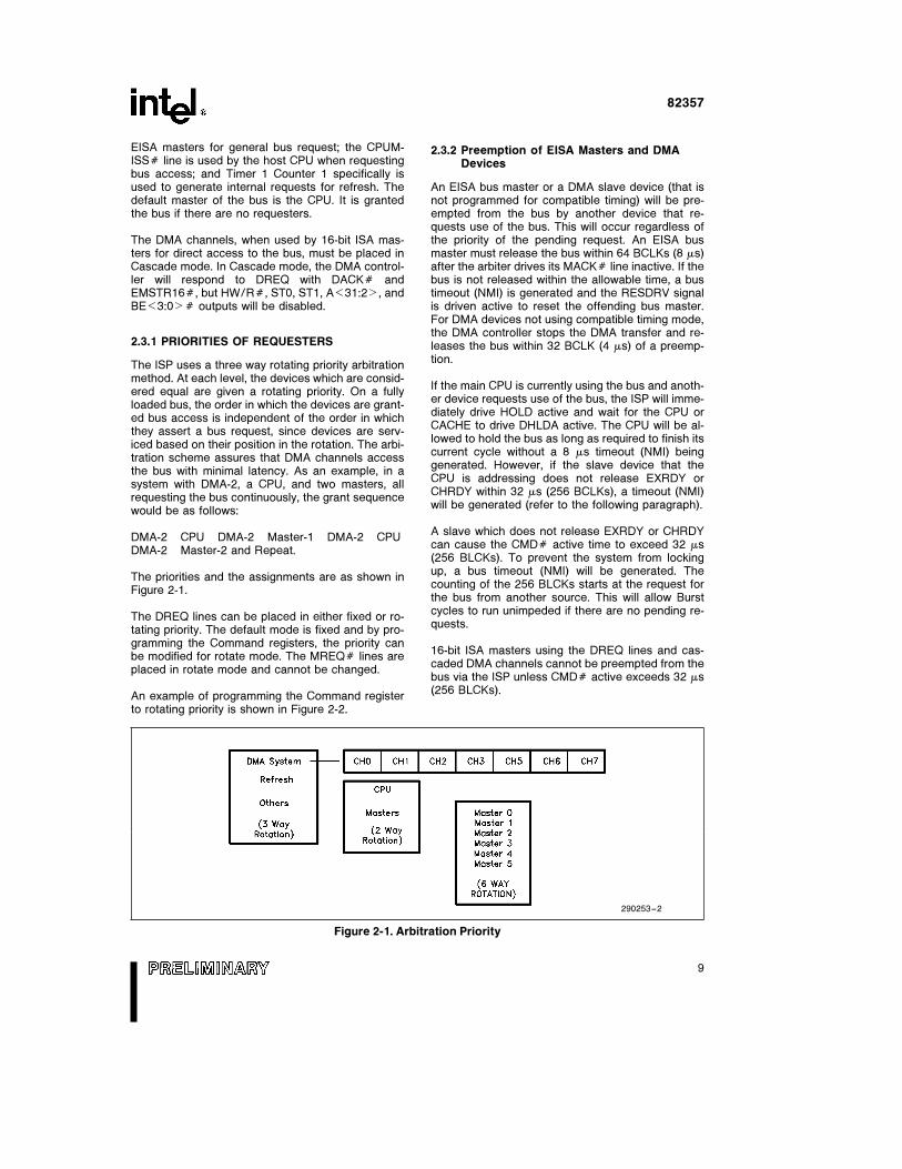
2.3.1 PRIORITIES OF REQUESTERS
The ISP uses a three way rotating priority arbitrationmethod. At each level, the devices which are consid-ered equal are given a rotating priority. On a fullyloaded bus, the order in which the devices are grant-ed bus access is independent of the order in whichthey assert a bus request, since devices are serv-iced based on their position in the rotation. The arbi-tration scheme assures that DMA channels accessthe bus with minimal latency. As an example, in asystem with DMA-2, a CPU, and two masters, allrequesting the bus continuously, the grant sequencewould be as follows:
DMA-2 CPU DMA-2 Master-1 DMA-2 CPUDMA-2 Master-2 and Repeat.
The priorities and the assignments are as shown inFigure 2-1.
The DREQ lines can be placed in either fixed or ro-tating priority. The default mode is fixed and by pro-gramming the Command registers, the priority canbe modified for rotate mode. The MREQÝ lines areplaced in rotate mode and cannot be changed.
An example of programming the Command registerto rotating priority is shown in Figure 2-2.
2.3.2 Preemption of EISA Masters and DMADevices
An EISA bus master or a DMA slave device (that isnot programmed for compatible timing) will be pre-empted from the bus by another device that re-quests use of the bus. This will occur regardless ofthe priority of the pending request. An EISA busmaster must release the bus within 64 BCLKs (8 ms)after the arbiter drives its MACKÝ line inactive. If thebus is not released within the allowable time, a bustimeout (NMI) is generated and the RESDRV signalis driven active to reset the offending bus master.For DMA devices not using compatible timing mode,the DMA controller stops the DMA transfer and re-leases the bus within 32 BCLK (4 ms) of a preemp-tion.
If the main CPU is currently using the bus and anoth-er device requests use of the bus, the ISP will imme-diately drive HOLD active and wait for the CPU orCACHE to drive DHLDA active. The CPU will be al-lowed to hold the bus as long as required to finish itscurrent cycle without a 8 ms timeout (NMI) beinggenerated. However, if the slave device that theCPU is addressing does not release EXRDY orCHRDY within 32 ms (256 BCLKs), a timeout (NMI)will be generated (refer to the following paragraph).
A slave which does not release EXRDY or CHRDYcan cause the CMDÝ active time to exceed 32 ms(256 BLCKs). To prevent the system from lockingup, a bus timeout (NMI) will be generated. Thecounting of the 256 BLCKs starts at the request forthe bus from another source. This will allow Burstcycles to run unimpeded if there are no pending re-quests.
16-bit ISA masters using the DREQ lines and cas-caded DMA channels cannot be preempted from thebus via the ISP unless CMDÝ active exceeds 32 ms(256 BLCKs).
290253–2
Figure 2-1. Arbitration Priority
9

82357
290253–3
Figure 2-2. DMA Channels in Rotating Priority
2.3.3 ARBITRATION DURING NON-MASKABLEINTERRUPTS
If a non-maskable interrupt (NMI) is pending at theCPU, and the CPU is requesting the bus, then theexternal bus masters and the DMA controller will beby-passed each time they come up for rotation. Thiswill give the CPU the bus bandwidth it requires toprocess the interrupt as fast as possible. The busmasters will still execute if the CPU is able to exe-cute out of a local cache and does not require thebus.
2.3.4 DREQ AND DACK LATENCY CONTROL
The ISP arbiter maintains a minimum DREQ toDACK latency on DMA channels programmed to op-erate in compatible timing mode. This is to supportolder devices such as the 8272A. This is implement-ed as an eight BCLK delay for DREQs coming intothe Priority resolution logic. The DREQs are effec-tively delayed by eight BCLKs prior to being seen bythe arbiter logic. Software requests will not have thisminimum request to DACK latency.
2.4 Refresh Generation
The refresh system uses the combined functions ofthe Interval Counter/Timers, Arbiter, and DMA. In-terval Counter 1/Timer 1 generates an internal re-
fresh request, the Arbiter detects a Refresh signalfrom either the Counter/Timer or the REFRESHÝinput and determines when the refresh will be done,and the DMA drives the refresh address out onto thehost bus. Counter 1 Timer 1 should be programmedto provide a request for refresh about every 15 ms.
Requests for refresh cycles are generated by twosources: Timer 1 Counter 1 and 16-bit ISA mastersthat activate REFRESHÝ when they have bus own-ership. EISA bus masters need not supply refreshcycles since the refresh controller can preempt thebus master and perform the necessary refresh cy-cles. 16-bit ISA bus masters that hold the bus longerthan 15 ms must supply memory refresh cycles.
Each time an internal refresh request is not servicedwithin the normal 15 ms interval, a counter is incre-mented. The counter counts up to four incompleterefresh requests. When a request cycle occurs, thepending refresh counter is decremented. Only onerefresh cycle will be run and the bus will be releasedto the requester with the highest priority. If more re-freshes are queued up, the bus will immediately bearbitrated for again, without waiting for the normal15 ms interval. If a refresh request is sensed whilefour refresh requests are pending, the incoming re-fresh request will be dropped. The bus is requestedwhenever one or more pending refreshes are re-corded.
10
82357
The DMA controller drives the refresh address outonto the LAk15:2l address bus (14 bits of refreshaddress) and also enables the BEk3:0lÝ lines sothat they can be translated to SAk1:0l lines. TheHigh and Low Page register contents will also beplaced on the LAk31:16l bus during refresh. Therefresh cycle lasts from the leading edge ofSTARTÝ through the rising edge of CMDÝ (twoBCLKs) unless wait states are added by the memoryslave negating EXRDY (EISA slaves) or CHRDY(ISA slaves). The 82358 bus controller, upon seeingREFRESHÝ, knows to run refresh cycles instead ofDMA cycles.
The refresh address bit order on the LAk15:2l andSAk15:0l bus is as follows:
13 12 11 10 9 8 1 0 7 6 5 4 3 2 1 0 Refresh
Counter Bits
15 14 13 12 11 10 9 8 7 6 5 4 3 2 1 0 LAk l,
SAk l
Addresses
The 14-bit refresh counter will be reset to 0 uponRST. The Page register is located at I/O address08FH and can be either read or written. The refreshHigh Page register is located at I/O address 048FHand can also be either read or written. When writingto the Low Page register, the upper Page register isnot cleared to zero.
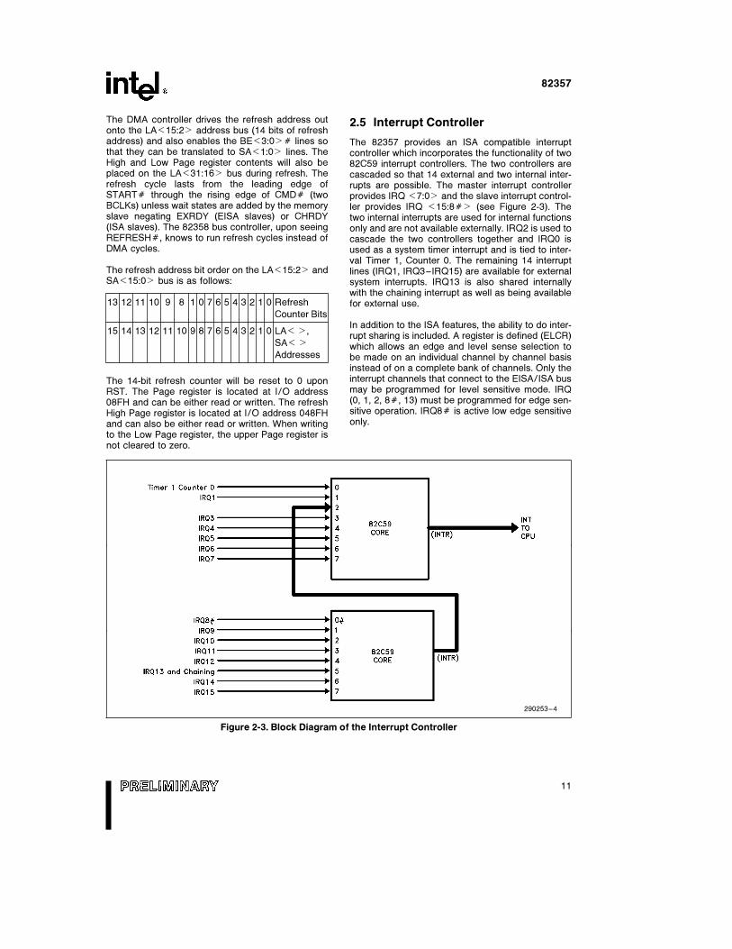
2.5 Interrupt Controller
The 82357 provides an ISA compatible interruptcontroller which incorporates the functionality of two82C59 interrupt controllers. The two controllers arecascaded so that 14 external and two internal inter-rupts are possible. The master interrupt controllerprovides IRQ k7:0l and the slave interrupt control-ler provides IRQ k15:8Ýl (see Figure 2-3). Thetwo internal interrupts are used for internal functionsonly and are not available externally. IRQ2 is used tocascade the two controllers together and IRQ0 isused as a system timer interrupt and is tied to inter-val Timer 1, Counter 0. The remaining 14 interruptlines (IRQ1, IRQ3–IRQ15) are available for externalsystem interrupts. IRQ13 is also shared internallywith the chaining interrupt as well as being availablefor external use.
In addition to the ISA features, the ability to do inter-rupt sharing is included. A register is defined (ELCR)which allows an edge and level sense selection tobe made on an individual channel by channel basisinstead of on a complete bank of channels. Only theinterrupt channels that connect to the EISA/ISA busmay be programmed for level sensitive mode. IRQ(0, 1, 2, 8Ý, 13) must be programmed for edge sen-sitive operation. IRQ8Ý is active low edge sensitiveonly.
290253–4
Figure 2-3. Block Diagram of the Interrupt Controller
11

82357
2.6 Non-Maskable Interrupt (NMI)
An NMI is an interrupt requiring immediate attentionand has priority over the normal interrupt lines(IRQX). The 82357 indicates error conditions bygenerating a non-maskable interrupt. An NMI can becaused by either a hardware or software mecha-nism.
NMI interrupts are caused by the following condi-tions:
1. Parity errors on the mother board memory. Thesystem board reports any parity errors from itsmemory system on the PARITYÝ line.
2. Parity errors on the add-in memory boards on theISA expansion bus. IOCHKÝ is driven low whenthis error occurs.
3. Timeout of the fail-safe timer Counter 0 on theinterval Timer 2 used to prevent the system fromlocking up. This NMI is sensed with a rising edgedetect latch.
4. Timeout of an 8 ms 32-bit ‘‘bus’’ master timeout. Ifa 32-bit bus master retains the bus more than 8ms after MACKÝ goes inactive, the 82357 willdrive the NMI and RESDRV signals active togeth-er. The RESDRV signal will remain active until theNMI has been reset.
NOTE:An NMI will not be generated in the case of theCPU holding onto the bus longer than the 8 mstimeout.
5. Timeout of the 32 ms CMDÝ active timer.
6. Software writing to the NMI I/O interrupt port(0462H). This is a special port which, when writ-ten, causes an immediate NMI interrupt, providedport 070h is enabled.
The NMI logic incorporates four different 8-bit regis-ters. These registers are addressed as Port(061h),Port(070h), Port(0461h), and Port(0462h). Thestatus of Ports (0461h) and (061h) are read by theCPU to determine which source caused the NMI.Bits set to 1 in these ports show which device re-quested an NMI interrupt. After the NMI interruptroutine processes the interrupt, the NMI status bitsare cleared by the software. This is done by set-ting the corresponding enable/disable bit high.Port(070h) is the mask register for the NMI inter-rupts. This register can mask the NMI signal andalso disable or enable all NMI sources. Writing toPort(0462h) with any data will cause an immediateNMI interrupt if enabled.
If it is desired to reset the system bus without reset-ting other devices in the system (standard systemboard devices are not reset), the Port(0461h) Bitk0l can be written with a (1). This bit should beheld in this state for the desired RSTDRV active timeand then returned to its normal state (0).
If a 32-bit bus master tries to hold the bus beyondthe 8 ms limit, or if CMDÝ is active for more than32 ms, the ISP will drive the NMI and RSTDRV sig-nals active together. The RSTDRV signal will remainactive until the NMI has been reset by resetting bitk3l to 0 in I/O Port 0461h.
NMI Source Enable/Disable and Status Port Bits
NMI SourceIO Port Bit IO Port Bit
for Status Reads for Enable/Disable
PARITYÝ Port 061h, Bit 7 Port 061h, Bit 2
Fail Safe Timer Port 0461h, Bit 7 Port 0461h, Bit 2
IOCHKÝ Port 061h, Bit 6 Port 061h, Bit 3
Bus Timeout Port 0461h, bit 6 Port 0461h, Bit 3
Write to Port 0462h Port 0461h, Bit 5 Port 0461h, Bit 1
12
82357
To ensure that all NMI requests are serviced, theNMI service routine software needs to incorporate afew very specific requirements. These requirementsare due to the edge detect circuitry of the host mi-croprocessor, 80386 or 80486. The software flowwould need to be the following:
1. NMI is detected by the processor on the risingedge of the NMI input.
2. The processor will read the status stored in Ports061h, and 0461h to determine what sourcescaused the NMI. The processor may then resetthe register bits controlling the sources that it hasdetermined to be active. Between the time theprocessor reads the NMI sources and resetsthem, an NMI may have been generated by an-other source. The level of the NMI will then re-main active. This new NMI source will not be rec-ognized by the processor because there was noedge on NMI.
3. The processor must then disable all NMI’s by writ-ing Bit k7l of Port 070h high and then enable allNMI’s by writing Bit k7l of Port 070h low. Thiswill cause the NMI output to transition low thenhigh if there are any pending NMI sources. TheCPU’s NMI input logic will then register a newNMI.
2.7 Interval Timers
The 82357 contains five counter/timers that areequivalent to those found in the 82C54 programma-ble interval timer. The counter timers are addressedas though they are contained in two separate 82C54timers. Timer 1 contains three counters and Timer 2contains two counters. Counter 1 of Timer 2 is notimplemented in EISA systems. Each timer providesthree frequencies or counters for the system. The8 MHz counters use BCLK for a clock source; theothers use a division of the 14.31818 MHz OSC in-put. The 14.31818 MHz OSC input is either dividedby 12 or 48 to provide the necessary frequencies.
The outputs of the timers are directed to key systemfunctions. Interval Timer 1, Counter 0 is connectedto the interrupt controller IRQ0 and provides a sys-tem timer interrupt for a time-of-day, diskette time-out, or other system timing functions. Counter 1generates a refresh-request signal and Counter 2generates the tone for the speaker.
Interval Timer 2, Counter 0 is the fail-safe timer thatcan generate NMI interrupts on the NMI line at regu-lar intervals as a means of preventing the systemfrom locking up. Counter 1 is not implemented.Counter 2 is used to slow down the CPU by meansof pulse-width modulation and is tied to theSLOWHÝ output. To use the slow function, thecounter must be programmed. If the counter is notprogrammed, SLOWHÝ will not go active. Counter 2is placed in the one-shot mode and is triggered bythe refresh request signal generated by Timer 1/Counter 1 only. If the counter has been pro-grammed, the Counter 2 output (SLOWHÝ) will stopthe CPU for the programmed period of the one-shotevery time a refresh request occurs. To enable theone-shot, select Mode 1 (one-shot) operation bywriting to I/O address 4Bh a value of 92h.
NOTE:Refresh cycles will not necessarily be generatedduring the time the SLOWHÝ signal is active, theArbiter will determine when the refresh cycle will beplaced on the bus.
Because the slow function depends upon the re-fresh-request frequency of another counter, chainingthe refresh-request frequency will affect the periodof Counter 2 output (SLOWHÝ) signal. Timer 2Counter 2 is not configured for the one-shot modeand is not programmed for a counter value until aspeed reduction in the system is required. At suchtime, the value programmed depends on the systemspeed desired.
13
82357
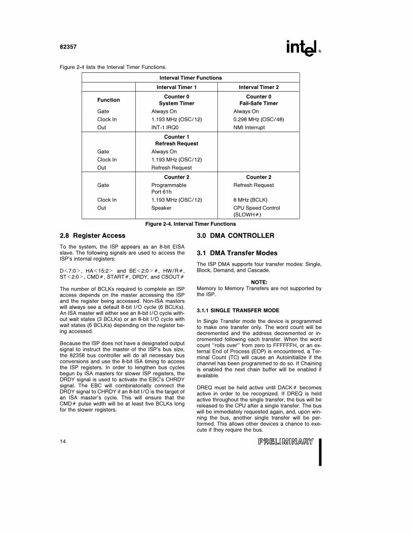
Figure 2-4 lists the Interval Timer Functions.
Interval Timer Functions
Interval Timer 1 Interval Timer 2
FunctionCounter 0 Counter 0
System Timer Fail-Safe Timer
Gate Always On Always On
Clock In 1.193 MHz (OSC/12) 0.298 MHz (OSC/48)
Out INT-1 IRQ0 NMI Interrupt
Counter 1
Refresh Request
Gate Always On
Clock In 1.193 MHz (OSC/12)
Out Refresh Request
Counter 2 Counter 2
Gate Programmable Refresh Request
Port 61h
Clock In 1.193 MHz (OSC/12) 8 MHz (BCLK)
Out Speaker CPU Speed Control
(SLOWHÝ)
Figure 2-4. Interval Timer Functions
2.8 Register Access
To the system, the ISP appears as an 8-bit EISAslave. The following signals are used to access theISP’s internal registers:
Dk7:0l, HAk15:2l and BEk2:0lÝ, HW/RÝ,STk2:0l, CMDÝ, STARTÝ, DRDY, and CSOUTÝ
The number of BCLKs required to complete an ISPaccess depends on the master accessing the ISPand the register being accessed. Non-ISA masterswill always see a default 8-bit I/O cycle (6 BCLKs).An ISA master will either see an 8-bit I/O cycle with-out wait states (3 BCLKs) or an 8-bit I/O cycle withwait states (6 BCLKs) depending on the register be-ing accessed.
Because the ISP does not have a designated outputsignal to instruct the master of the ISP’s bus size,the 82358 bus controller will do all necessary busconversions and use the 8-bit ISA timing to accessthe ISP registers. In order to lengthen bus cyclesbegun by ISA masters for slower ISP registers, theDRDY signal is used to activate the EBC’s CHRDYsignal. The EBC will combinatorially connect theDRDY signal to CHRDY if an 8-bit I/O is the target ofan ISA master’s cycle. This will ensure that theCMDÝ pulse width will be at least five BCLKs longfor the slower registers.
3.0 DMA CONTROLLER
3.1 DMA Transfer Modes
The ISP DMA supports four transfer modes: Single,Block, Demand, and Cascade.
NOTE:Memory to Memory Transfers are not supported bythe ISP.
3.1.1 SINGLE TRANSFER MODE
In Single Transfer mode the device is programmedto make one transfer only. The word count will bedecremented and the address decremented or in-cremented following each transfer. When the wordcount ‘‘rolls over’’ from zero to FFFFFFH, or an ex-ternal End of Process (EOP) is encountered, a Ter-minal Count (TC) will cause an Autoinitialize if thechannel has been programmed to do so. If Chainingis enabled the next chain buffer will be enabled ifavailable.
DREQ must be held active until DACKÝ becomesactive in order to be recognized. If DREQ is heldactive throughout the single transfer, the bus will bereleased to the CPU after a single transfer. The buswill be immediately requested again, and, upon win-ning the bus, another single transfer will be per-formed. This allows other devices a chance to exe-cute if they require the bus.
14

82357
3.1.2 BLOCK TRANSFER MODE
In Block Transfer mode the device is activated byDREQ to continue making transfers during the serv-ice until a TC, caused by word count going toFFFFFFH, or an external EOP, is encountered.DREQ need only be held active until DACK be-comes active. An Autoinitialization will occur at theend of the service if the channel has been pro-grammed for it. In this mode, it is possible to lock outother devices for a period of time (including refresh)if the transfer count is programmed to a large num-ber.
3.1.3 DEMAND TRANSFER MODE
In Demand Transfer mode the device is pro-grammed to continue making transfers until a TC isencountered or an external EOP is encountered, oruntil DREQ goes inactive. Thus transfers may con-tinue until the I/O device has exhausted its data ca-pacity. After the I/O device has had a chance tocatch up, the DMA service is reestablished bymeans of a DREQ. During the time between serviceswhen the system is allowed to operate, the interme-diate values of address and word count are stored inthe DMA controller Current Address and CurrentWord Count registers. A TC can cause an Autoinitial-ize at the end of the service if the channel has beenprogrammed for it.
3.1.4 CASCADE MODE
This mode is used to cascade more than one DMAcontroller together for simple system expansion.This allows the DMA requests of the additional de-vice to propagate through the priority network cir-cuitry of the preceding device. The priority chain ispreserved and the new device must wait for its turnto acknowledge requests. In this architecture, Chan-nel 0 of the second controller (ch4) is used to cas-cade the first controller to provide a total of sevenchannels.
Cascade mode is also used to allow direct access ofthe system by 16-bit ISA bus masters. These devic-es use the DREQ and DACK signals to arbitrate forthe system bus and then they drive the address andcommand lines to control the bus.
In Cascade Mode, the DMA controller will respondto DREQ with DACKÝ but the HW/RÝ, address,and ST0–ST3 outputs will be disabled.
Channel 4 is used to connect the second half of theDMA system, this channel is not available for anyother purpose.
3.2 Transfer Types
Each of the three active transfer modes can performthree different types of transfers. These are Read,Write and Verify.
3.2.1 WRITE TRANSFER
Write transfers move data from an I/O device tomemory starting with the DMA activating HW/RÝand the STk3:0l lines, the Bus Controller will thenactivate IORCÝ and the appropriate EISA or ISAcontrol signals to indicate a memory write dependingon which bus the memory is determined to be.
3.2.2 READ TRANSFER
Read transfers move data from memory to an I/Odevice starting with the DMA deactivating HW/RÝand activating the STk3:0l lines, the Bus Control-ler will then activate IOWCÝ and the appropriateEISA or ISA control signals to indicate a memoryread, depending on which bus the memory is deter-mined to be.
3.2.3 VERIFY TRANSFER
Verify transfers are pseudo transfers. The DMA con-troller operates as in Read or Write transfers gener-ating addresses, and producing TC, etc. However,no STk3:0l signals are activated so the Bus Con-troller does not activate the memory and I/O controllines. Only the DACK lines will go active. Since noEISA cycles are broadcasted in this mode, the LAbus is not copied to the SA bus. Internally the DMAcontroller will count BCLKs so that the DACK lineshave a defined pulse width. This pulse width is nineBCLKs long. If Verify transfers are repeated duringBlock or Demand DMA requests, each additionalpseudo transfer will add eight BCLKs. The DACKlines will not be toggled for repeated transfers.
3.3 Autoinitialize
By programming a bit in the Mode register, a chan-nel may be set up as an Autoinitialize channel. Dur-ing Autoinitialize initialization, the original values ofthe Current page, Current address and Current WordCount registers are automatically restored from theBase Page, Address, and Word count registers ofthat channel following TC. The Base registers areloaded simultaneously with the Current registers bythe microprocessor and remain unchanged through-out the DMA service. The mask bit is not set whenthe channel is in Autoinitialize. Following Autoinitial-ize the channel is ready to perform another DMAservice, without CPU intervention, as soon as a validDREQ is detected.
15
82357
3.4 Channel Priority
For priority resolution the DMA consists of two logi-cal channel groupsÐchannels 0–3 and channels4–7. Each group may be in either Fixed or Rotatemode, as determined by the Command register.
3.4.1 FIXED PRIORITY
The initial fixed priority structure is as follows:
High priority Low priority
(0, 1, 2, 3) 5, 6, 7
Channel 0 has the highest priority, then 1, 2, 3, 5, 6,and channel 7 has the lowest priority.
3.4.2 ROTATING PRIORITY
Rotation allows for ‘‘fairness’’ in priority resolution.The priority chain rotates so that the last channelserviced is assigned the lowest priority in the chan-nel group (0–3, 5–7).
Channels 0–3 rotate as a group 4, and are alwaysplaced between Channel 5 and Channel 7 in the pri-ority list.
Channels 5–7 rotate as a group of 4Ðthis is, thethree channels (5–7) plus the channel 0–3 group.
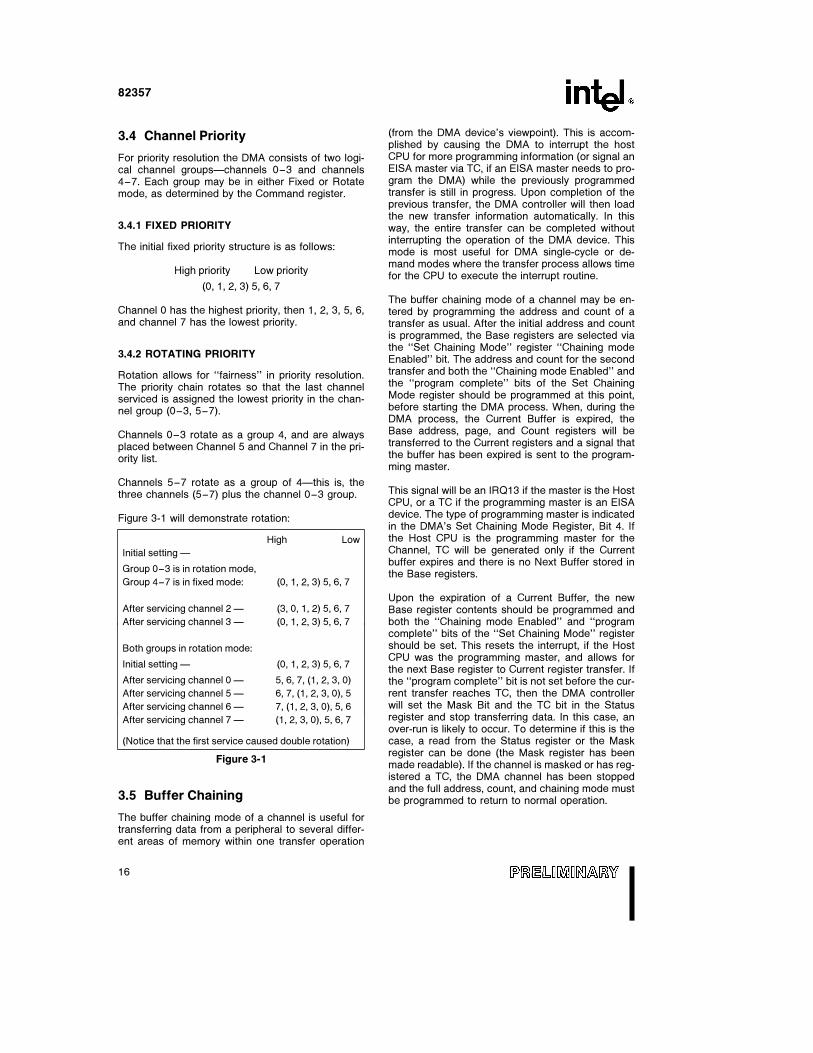
Figure 3-1 will demonstrate rotation:
High Low
Initial setting Ð
Group 0–3 is in rotation mode,
Group 4–7 is in fixed mode: (0, 1, 2, 3) 5, 6, 7
After servicing channel 2 Ð (3, 0, 1, 2) 5, 6, 7
After servicing channel 3 Ð (0, 1, 2, 3) 5, 6, 7
Both groups in rotation mode:
Initial setting Ð (0, 1, 2, 3) 5, 6, 7
After servicing channel 0 Ð 5, 6, 7, (1, 2, 3, 0)
After servicing channel 5 Ð 6, 7, (1, 2, 3, 0), 5
After servicing channel 6 Ð 7, (1, 2, 3, 0), 5, 6
After servicing channel 7 Ð (1, 2, 3, 0), 5, 6, 7
(Notice that the first service caused double rotation)
Figure 3-1
3.5 Buffer Chaining
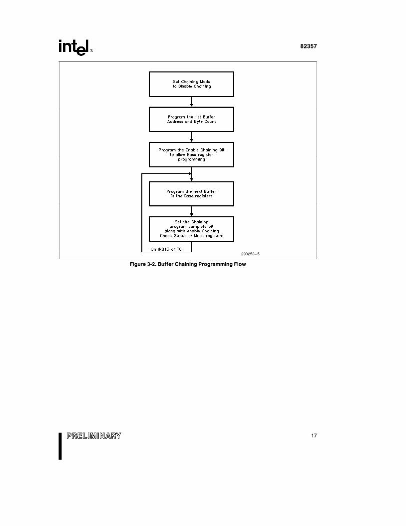
The buffer chaining mode of a channel is useful fortransferring data from a peripheral to several differ-ent areas of memory within one transfer operation
(from the DMA device’s viewpoint). This is accom-plished by causing the DMA to interrupt the hostCPU for more programming information (or signal anEISA master via TC, if an EISA master needs to pro-gram the DMA) while the previously programmedtransfer is still in progress. Upon completion of theprevious transfer, the DMA controller will then loadthe new transfer information automatically. In thisway, the entire transfer can be completed withoutinterrupting the operation of the DMA device. Thismode is most useful for DMA single-cycle or de-mand modes where the transfer process allows timefor the CPU to execute the interrupt routine.
The buffer chaining mode of a channel may be en-tered by programming the address and count of atransfer as usual. After the initial address and countis programmed, the Base registers are selected viathe ‘‘Set Chaining Mode’’ register ‘‘Chaining modeEnabled’’ bit. The address and count for the secondtransfer and both the ‘‘Chaining mode Enabled’’ andthe ‘‘program complete’’ bits of the Set ChainingMode register should be programmed at this point,before starting the DMA process. When, during theDMA process, the Current Buffer is expired, theBase address, page, and Count registers will betransferred to the Current registers and a signal thatthe buffer has been expired is sent to the program-ming master.
This signal will be an IRQ13 if the master is the HostCPU, or a TC if the programming master is an EISAdevice. The type of programming master is indicatedin the DMA’s Set Chaining Mode Register, Bit 4. Ifthe Host CPU is the programming master for theChannel, TC will be generated only if the Currentbuffer expires and there is no Next Buffer stored inthe Base registers.
Upon the expiration of a Current Buffer, the newBase register contents should be programmed andboth the ‘‘Chaining mode Enabled’’ and ‘‘programcomplete’’ bits of the ‘‘Set Chaining Mode’’ registershould be set. This resets the interrupt, if the HostCPU was the programming master, and allows forthe next Base register to Current register transfer. Ifthe ‘‘program complete’’ bit is not set before the cur-rent transfer reaches TC, then the DMA controllerwill set the Mask Bit and the TC bit in the Statusregister and stop transferring data. In this case, anover-run is likely to occur. To determine if this is thecase, a read from the Status register or the Maskregister can be done (the Mask register has beenmade readable). If the channel is masked or has reg-istered a TC, the DMA channel has been stoppedand the full address, count, and chaining mode mustbe programmed to return to normal operation.
16
82357
290253–5
Figure 3-2. Buffer Chaining Programming Flow
17
82357
Note that if the Host CPU is the programming mas-ter, an interrupt will only be generated if a CurrentBuffer expires and chaining mode is enabled, it willnot occur during initial programming. The ‘‘ChannelInterrupt Status’’ register will indicate pending inter-rupts only. That is, it will indicate an empty Baseregister with ‘‘Chaining Mode’’ enabled. WhenChaining mode is enabled, only the Base registersare written by the processor, and only the Currentregisters can be read. The Current registers are onlyupdated on a TC.
3.6 DMA Enhanced Timing
3.6.1 COMPATIBLE TIMING
Compatible timing is provided for DMA slave devic-es, which, due to some design limitation, cannotsupport one of the faster timings. Compatible timingruns at 1125 ns/single cycle and 1000 ns/cycle dur-ing the repeated portion of a BLOCK or DEMANDmode transfer.
3.6.2 TYPE ‘‘A’’ TIMING
Type ‘‘A’’ timing is provided to allow shorter cycleswhen used with EISA memory. If 8/16-bit ISA mem-ory is decoded, the system automatically reverts toISA DMA type compatible timing on a cycle-by-cyclebasis. Type ‘‘A’’ timing runs at 875 ns/single cycleand 750 ns/cycle during the repeated portion of aBLOCK or DEMAND mode transfer. Type ‘‘A’’ timingvaries from compatible timing primarily in shorteningthe memory operation to the minimum allowed byEISA memory. The I/O portion of the cycle (datasetup or write, I/O read access time) is the same aswith compatible cycles. The actual active commandtime is shorter, but it is expected that the DMA de-vices which provide the data access time or writedata setup time should not require excess IORCÝ orIOWCÝ command active time. Because of this,most ISA DMA devices should be able to use type‘‘A’’ timing.
3.6.3 TYPE ‘‘B’’ TIMING
Type ‘‘B’’ timing is provided for 8/16-bit ISA or EISADMA I/O devices which can accept faster I/O tim-ing. Type ‘‘B’’ only works with EISA memory. If 8/16-bit ISA memory is decoded, the system automatical-ly reverts to ISA DMA type compatible timing on acycle by cycle basis. Type ‘‘B’’ timing runs at 750ns/single cycle and 500 ns/cycle during the repeat-ed portion of a BLOCK or DEMAND mode transfer.Type ‘‘B’’ timing requires faster DMA slave devicesthan compatible timing in that the cycles are short-ened so that the data setup time on I/O write cycles
is shortened and the I/O read access time is re-quired to be faster. Some of the current ISA devicesshould be able to support type ‘‘B’’ timing, but thesewill probably be more recent designs using relativelyfast technology.
3.6.4 TYPE ‘‘C’’ (BURST TIMING)
Burst timing is provided for newly designed EISADMA devices. The DMA slave device needs to moni-tor the EXRDY and IORCÝ or IOWCÝ signals todetermine when to change the data (on writes) orsample the data (on reads). This timing will allow upto 33 Mbytes per second transfer rate with a 32-bitDMA device and 32-bit memory. Note that 8- or 16-bit DMA devices are supported (through the pro-grammable DMA address increment) and that theyuse the ‘‘byte lanes’’ natural to their size for the datatransfer. As with all bursts, the system will revert totwo BCLK cycles if the memory does not supportburst. When a DMA burst cycle accesses non-burstmemory and the DMA cycle crosses a page bounda-ry into burstable memory, the EBC will continue per-forming non-burst cycles. This will not cause a prob-lem since the data is transferred correctly.
3.7 Register Description
DMA Channel 4 is used to cascade the two DMAcontrollers together and should not be programmedfor any mode other than cascade. The Mode registerwill default to cascade mode. Special attentionshould also be taken when programming the Com-mand and Mask registers as related to channel 4(refer to the Command and Mask register descrip-tions, Sections 3.7.7 and 3.7.11).
3.7.1. STOP REGISTERS (RING BUFFERDATA STRUCTURE)
To support a common data communication datastructure (the ring buffer), a set of new DMA regis-ters have been provided. These registers are calledStop registers. Each channel has 22-bits of registerlocation associated with it. The 22-bits is distributedbetween three different registers (one 6-bit and two8-bit). The Stop registers can be enabled or disabledby writing to the channel’s corresponding ExtendedMode register.
The ring buffer data structure reserves a fixed por-tion of memory, on doubleword boundaries, to beused for a DMA channel. Consecutively receivedframes or other data structures are stored sequen-tially within the boundaries of the ring buffer memo-ry.
18
82357
The beginning and end of the ring buffer area is de-fined in the Base Address register and the Base Ad-dress register a the Base Byte/Transfer Count. Theincoming frames (data) are deposited in sequentiallocations of the ring buffer. When the DMA reachesthe end of the ring buffer, indicating the byte counthas expired, the DMA controller (if so programmed)will Autoinitialize. Upon autoinitialization, the CurrentAddress register will be restored from the Base Ad-dress register, taking the process back to the start ofthe ring buffer. The DMA will then be available tobegin depositing the incoming bytes in the ring buff-ers sequential locationsÐproviding that the hostCPU has read the data that was previously placed inthose locations. The DMA determines that the CPUhas read certain data by the value that the CPUwrites into the Stop register.
Once the data of a frame is read by the CPU, thememory location it occupies becomes available forother incoming frames. The Stop register prevents
the DMA from over writing data that has not yetbeen read by the CPU. After the CPU has read aframe from memory it will update the Stop register topoint to the location that was last read. The DMA willnot deposit data into any location beyond that point-ed to by the Stop register. The last address trans-ferred before the channel is masked is the first ad-dress that matches the Stop register. (See Table3-1). The Stop registers store values to compareagainst Ak23:2l only, so the size of the ring bufferis limited to 16 Mbytes.
The Bus Controller provides I/O recovery for back-to-back CPU to 8-bit I/O cycles. For EISA masteraccesses, I/O recovery of at least one BCLK mustbe provided by software.
NOTE:I/O writes must match the I/O slave size (i.e., 8-bitwrites must be used to program the ISP registers).When writing to the DMA registers, the DMA chan-nels also must be masked.
For example:
If the stop register e 00001Ch, the last three transfers will be:
Table 3-1
By Bytes By Words By Dwords
Increment XX00001Ah XX000018h XX000014h
XX00001Bh XX00001Ah XX000018h
XX00001Ch XX00001Ch XX00001Ch
Decrement XX000021h XX000023h XX000027h
XX000020h XX000021h XX000023h
XX00001Fh XX00001Fh XX00001Fh
19
82357
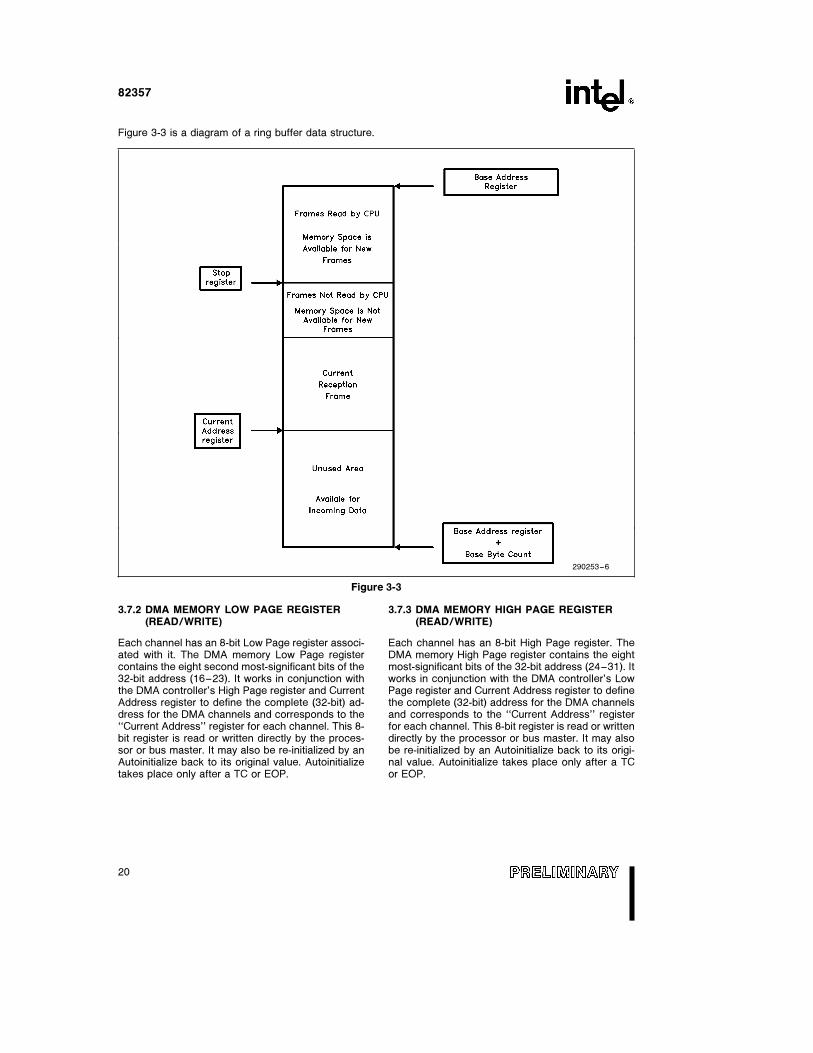
Figure 3-3 is a diagram of a ring buffer data structure.
290253–6
Figure 3-3
3.7.2 DMA MEMORY LOW PAGE REGISTER(READ/WRITE)
Each channel has an 8-bit Low Page register associ-ated with it. The DMA memory Low Page registercontains the eight second most-significant bits of the32-bit address (16–23). It works in conjunction withthe DMA controller’s High Page register and CurrentAddress register to define the complete (32-bit) ad-dress for the DMA channels and corresponds to the‘‘Current Address’’ register for each channel. This 8-bit register is read or written directly by the proces-sor or bus master. It may also be re-initialized by anAutoinitialize back to its original value. Autoinitializetakes place only after a TC or EOP.
3.7.3 DMA MEMORY HIGH PAGE REGISTER(READ/WRITE)
Each channel has an 8-bit High Page register. TheDMA memory High Page register contains the eightmost-significant bits of the 32-bit address (24–31). Itworks in conjunction with the DMA controller’s LowPage register and Current Address register to definethe complete (32-bit) address for the DMA channelsand corresponds to the ‘‘Current Address’’ registerfor each channel. This 8-bit register is read or writtendirectly by the processor or bus master. It may alsobe re-initialized by an Autoinitialize back to its origi-nal value. Autoinitialize takes place only after a TCor EOP.
20
82357
This register is reset to 00h during the programmingof both the low page register and the Current Ad-dress register. Thus, if this register is not pro-grammed after the other address and Low Page reg-isters are programmed, then its value will be zero. Inthis case, the DMA channel will operate the same asan 82C37 (from an addressing standpoint). This isthe address compatibility mode.
If the high 8-bits of the address are programmedafter the other addresses, then the channel willmodify its operation to increment (or decrement) theentire 32-bit address. This is unlike the 82C37‘‘Page’’ register in the original PCs which could onlyincrement to a 64K boundary (for 8-bit channels) or128K (for 16-bit channels). This is extended addressmode. In this mode, the EISA bus controller shouldgenerate the signals MRDCÝ and MWTCÝ only foraddresses below 16 Mbytes.
3.7.3.1 Address Compatibility Mode
Whenever the DMA is operating in Address Compat-ibility mode, the addresses do not increment or dec-rement through the HIGH and LOW Page registers,and the high page register is set to 00h. This is com-patible with the 82C37 and Page register implemen-tation used in the PC AT*. This mode is set whenany of the lower three address bytes of a channelare programmed. If the upper byte of a channel’saddress is programmed last, the channel will go intoExtended Address Mode. In this mode the high bytemay be any value and the address will increment ordecrement through the entire 32-bits. When pro-gramming the page register in compatible mode, thecurrent address must also be programmed.
After RST all channels will be set to CompatibilityMode. The Master Clear command will also resetthe proper channels to Compatibility Mode. Themode bits are stored in individual flip-flops on a per-channel basis.
3.7.4 CURRENT ADDRESS REGISTER(READ/WRITE)
Each channel has a 16-bit Current Address register.This register holds the value of the 16 least signifi-cant bits (0–15) of the full 32-bit address used dur-ing DMA transfers. The address is automatically in-cremented or decremented after each transfer andthe intermediate values of the address are stored inthe Current Address register during the transfer. Thisregister is written to or read from by the microproc-essor or bus master in successive 8-bit bytes. It mayalso be re-initialized by an Autoinitialize back to itsoriginal value. Autoinitialize takes place only after aTC or EOP.
3.7.4.1 Address Shifting when Programmedfor 16-bit I/O Count by Words
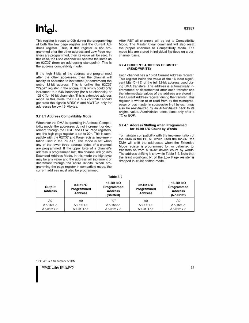
To maintain compatibility with the implementation ofthe DMA in the PC AT which used the 82C37, theDMA will shift the addresses when the ExtendedMode register is programmed for, or defaulted to,transfers to/from a 16-bit device count by words.The address shifting is shown in Table 3-2. Note thatthe least significant bit of the Low Page resister isdropped in 16-bit shifted mode.
Table 3-2
8-Bit I/O16-Bit I/O
32-Bit I/O16-Bit I/O
OutputProgrammed
ProgrammedProgrammed
Programmed
AddressAddress
AddressAddress
Address
(Shifted) (No Shift)
A0 A0 ‘‘0’’ A0 A0
Ak16:1l Ak16:1l Ak15:0l Ak16:1l Ak16:1l
Ak31:17l Ak31:17l Ak31:17l Ak31:17l Ak31:17l
* PC AT is a trademark of IBM.
21
82357
3.7.5 CURRENT WORD REGISTER(READ/WRITE)
Each channel has a 24-bit Current Word Count reg-ister. This register determines the number of trans-fers to be performed. The actual number of transferswill be one more than the number programmed inthe Current Word Count register (i.e., programming acount of 100 will result in 101 transfers). The wordcount is decremented after each transfer. The inter-mediate value of the word count is stored in theregister during the transfer. When the value in theregister goes from zero to 0FFFFFFH, a TC will begenerated.
Following the end of a DMA service it may also bere-initialized by an Autoinitialization back to its origi-nal value. Autoinitialize can occur only when a TCoccurs. If it is not Autoinitialized, this register willhave a count of FFFFFFH after TC.
To maintain compatibility with the 82C37, program-ming either the low byte, bitsk7:0l, or the middlebyte, bitsk15:8l, will clear the high bytebitsk23:16l. This provides compatibility with theprevious software that does not know of the exis-tence of the upper byte of the word count.
When the Extended Mode register is programmedfor, or defaulted to, transfers to/from an 8-bit I/O,the Word count will indicate the number of bytes tobe transferred.
When the Extended Mode register is programmedfor, or defaulted to, transfers to/from a 16-bit I/O,with shifted address, the Word count will indicate thenumber of 16-bit words to be transferred.
When the Extended Mode register is programmedfor transfers to/from a 16- or 32-bit I/O, the WordCount will indicate the number of bytes to be trans-ferred. The number of bytes does not need to be amultiple of two or four in this case.
3.7.6 BASE PAGE, BASE ADDRESS AND BASEWORD COUNT REGISTERS (WRITE ONLY)
Each channel has a set of Base Page, Base Addressand Base Word Count registers. These registersstore the original value of their associated Currentregisters. During Autoinitialize these values are usedto restore the Current registers to their original val-ues. The Base registers are written simultaneouslywith their corresponding Current register in 8-bitbytes in the Program Condition by the microproces-sor. These registers cannot be read by the micro-processor.
During Chaining Mode, these registers will store theinformation about the next buffer in the Chain, if pro-grammed.
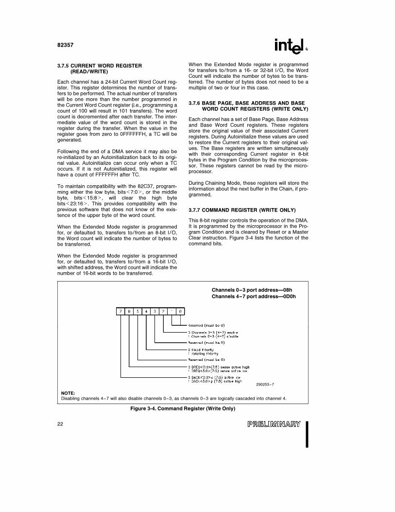
3.7.7 COMMAND REGISTER (WRITE ONLY)
This 8-bit register controls the operation of the DMA.It is programmed by the microprocessor in the Pro-gram Condition and is cleared by Reset or a MasterClear instruction. Figure 3-4 lists the function of thecommand bits.
Channels 0–3 port addressÐ08h
Channels 4–7 port addressÐ0D0h
290253–7
NOTE:Disabling channels 4–7 will also disable channels 0–3, as channels 0–3 are logically cascaded into channel 4.
Figure 3-4. Command Register (Write Only)
22
82357
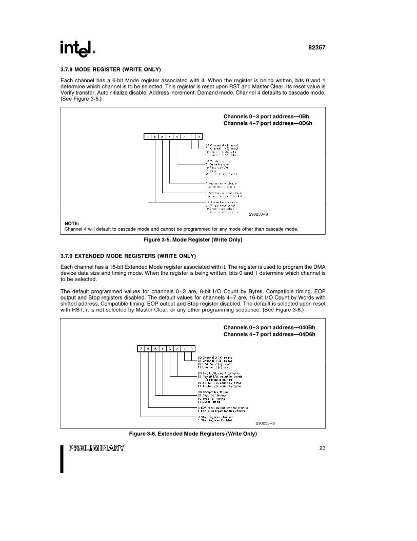
3.7.8 MODE REGISTER (WRITE ONLY)
Each channel has a 6-bit Mode register associated with it. When the register is being written, bits 0 and 1determine which channel is to be selected. This register is reset upon RST and Master Clear. Its reset value isVerify transfer, Autoinitialize disable, Address increment, Demand mode. Channel 4 defaults to cascade mode.(See Figure 3-5.)
Channels 0–3 port addressÐ0Bh
Channels 4–7 port addressÐ0D6h
290253–8
NOTE:Channel 4 will default to cascade mode and cannot be programmed for any mode other than cascade mode.
Figure 3-5. Mode Register (Write Only)
3.7.9 EXTENDED MODE REGISTERS (WRITE ONLY)
Each channel has a 16-bit Extended Mode register associated with it. The register is used to program the DMAdevice data size and timing mode. When the register is being written, bits 0 and 1 determine which channel isto be selected.
The default programmed values for channels 0–3 are, 8-bit I/O Count by Bytes, Compatible timing, EOPoutput and Stop registers disabled. The default values for channels 4–7 are, 16-bit I/O Count by Words withshifted address, Compatible timing, EOP output and Stop register disabled. The default is selected upon resetwith RST, it is not selected by Master Clear, or any other programming sequence. (See Figure 3-6.)
Channels 0–3 port addressÐ040Bh
Channels 4–7 port addressÐ04D6h
290253–9
Figure 3-6. Extended Mode Registers (Write Only)
23
82357
3.7.9.1 8-Bit I/O, ‘‘Count By Bytes’’ Mode
In 8-bit I/O, ‘‘count by bytes’’ mode, the addresscounter can be programmed to any address. Thecount register is programmed with the number ofbytes minus 1 to transfer. In this mode, byte assem-bly/disassembly is not available (or necessary) sothe timing used when 8- or 16-bit memory is sensedis compatible with the original ISA products.
3.7.9.2 16-Bit I/O, ‘‘Count By Words’’(Address Shifted) Mode
In ‘‘count by words’’ mode (address shifted), the ad-dress counter can be programmed to any even ad-dress, but must be programmed with the addressvalue shifted right by one bit. The Page registers arenot shifted, this results in the least significant bit ofthe Low Page register being ignored. In this mode,burst timing and byte assembly/disassembly is notavailable so the timing used when 8- or 16-bit mem-ory is sensed is compatible with the original ISAproducts. The Count register is programmed with thenumber of words minus 1 to be transferred.
3.7.9.3 16-Bit I/O, ‘‘Count By Bytes’’ Mode
In 16-bit ‘‘count by bytes’’ mode, the address coun-ter can be programmed to any byte address. Formost DMA devices, however, it should be pro-grammed only to even addresses. If the address isprogrammed to an odd address, the DMA controllerwill do a partial word transfer during the first and lasttransfer if necessary. The bus controller logic will dothe byte/word assembly necessary to read or writeany size memory device and both the DMA and buscontrollers support burst for this mode. In this mode,the Address register is incremented or decrementedby two and the byte count is decremented by thenumber of bytes transferred during each bus cycle.The Count register is programmed with the numberof bytes b1 to be transferred.
3.7.9.4 32-Bit I/O, ‘‘Count By Bytes’’ Mode
In 32-bit I/O ‘‘count by bytes’’ mode, the addresscounter can be programmed to any byte address.For most DMA devices, however, it should be pro-grammed only to addresses evenly divisible by four.
If the address is programmed to a value that is notdivisible by four, then the DMA controller will do par-tial transfers for the first and last transfers if neces-sary. The bus controller logic will do the byte/wordassembly necessary to read or write any size memo-ry device and both the DMA and bus controllers sup-port burst for this mode. In this mode, the Addressregister is incremented or decremented by four andthe byte count is decremented by the number ofbytes transferred during each bus cycle. The Countregister is programmed with the number of bytes mi-nus 1 to be transferred.
3.7.9.5 EOP Input/Output Selection
Bit 6 of the Extended Mode register selects whetherthe EOP signal is to be used as an input or an outputduring DMA transfers. The EOP I/O selection is pro-grammable on a channel by channel basis. EOP willgenerally be used as an output, as was available onthe PCAT. The input function was added to supportData Communication and other devices that wouldlike to trigger an autoinitialize when a collision orsome other event occurs. The direction of EOP isswitched when DACKÝ is changed. There may besome overlap of the ISP driving the EOP signalalong with the DMA slave, however, during this over-lap both devices will be driving the signal to a lowlevel (inactive).
3.7.9.6 Stop Register Selection
Bit 7 of this register selects whether the Stop regis-ters associated with this channel are to be used ornot. Normally the Stop Registers will not be used.This function was also added to help support DataCommunication or other devices that work from aRing Buffer in memory (refer to Section 3.7.1).
3.7.9.7 Summary of the DMA Transfer Sizes
Table 3-3 lists each of the DMA device transfersizes. The column labeled ‘‘Word Count register’’ in-dicates that the register contents represents eitherthe number of bytes to transfer or the number of16-bit words to transfer. The column labeled ‘‘Cur-rent Address Register Increment/Decrement’’ indi-cates the number added to or taken from the Cur-rent Address register after each DMA transfer cycle.The Mode Register determines if the Current Ad-dress register will be incremented or decremented.
Table 3-3
DMA Device Data Size Word Count Current Address
and Word Count Register Increment/Decrement
8-Bit I/O, Count by Bytes Bytes 116-Bit I/O, Count by Words Words 1(Address Shifted)16-Bit I/O, Count by Bytes Bytes 232-Bit I/O, Count by Bytes Bytes 4
24
82357
3.7.10 REQUEST REGISTER (WRITE ONLY)
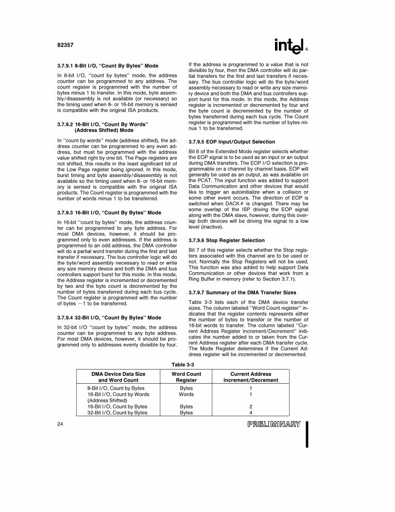
Each channel has a Request bit associated with it in one of the two 4-bit Request registers. The Requestregister is used by software to initiate a DMA request. The DMA responds to the software request as thoughDREQkxl is active. These requests are non-maskable and subject to prioritization by the Priority Encodernetwork (refer to Section 3.4). Each register bit is set or reset separately under software control or is clearedupon generation of a TC. The entire register is cleared upon RST, it is not cleared upon a RSTDRV output. Toset or reset a bit, the software loads the proper form of the data word. When the register is being written, bits 0and 1 determine which channel is to be selected. In order to make a software request, the channel must be inBlock Mode. (See Figure 3-7.)
Channels 0–3 port addressÐ09h
Channels 4–7 port addressÐ0D2h
290253–10
Figure 3-7. Request Register (Write Only)
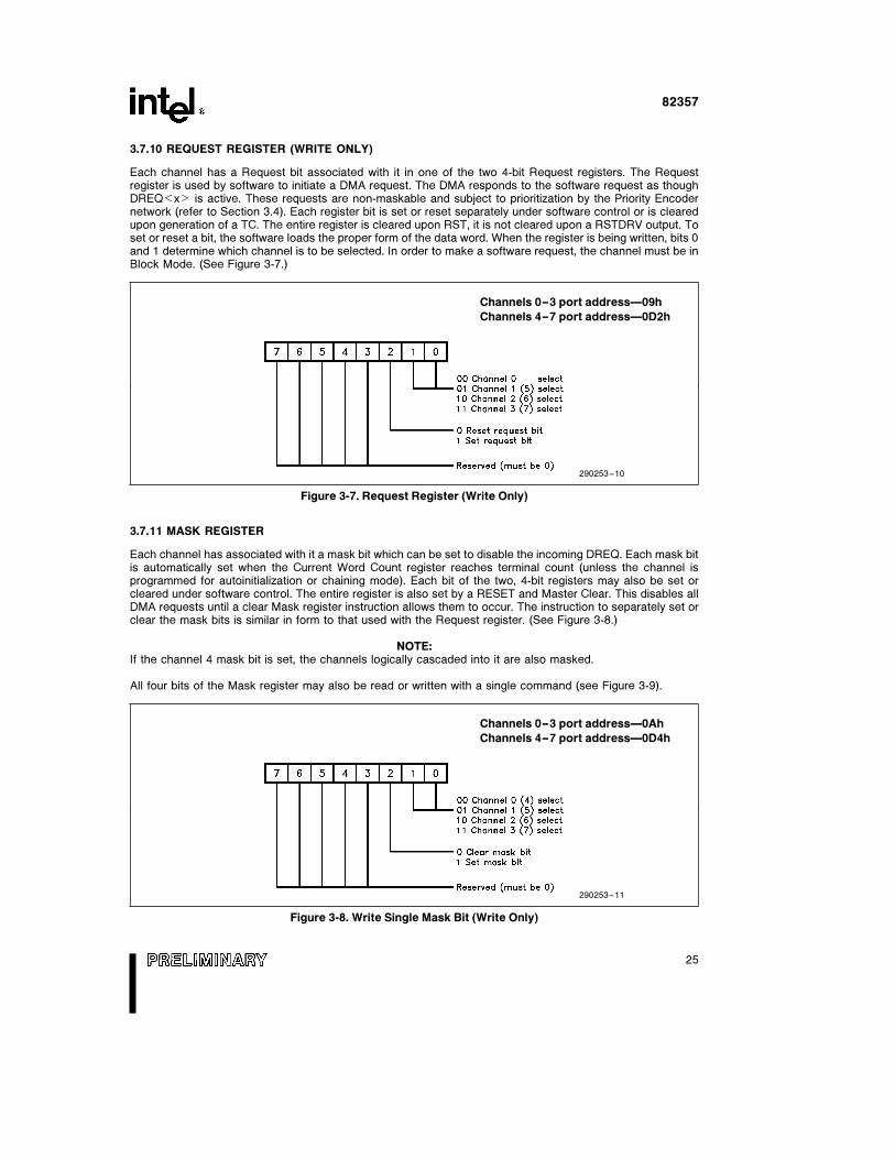
3.7.11 MASK REGISTER
Each channel has associated with it a mask bit which can be set to disable the incoming DREQ. Each mask bitis automatically set when the Current Word Count register reaches terminal count (unless the channel isprogrammed for autoinitialization or chaining mode). Each bit of the two, 4-bit registers may also be set orcleared under software control. The entire register is also set by a RESET and Master Clear. This disables allDMA requests until a clear Mask register instruction allows them to occur. The instruction to separately set orclear the mask bits is similar in form to that used with the Request register. (See Figure 3-8.)
NOTE:If the channel 4 mask bit is set, the channels logically cascaded into it are also masked.
All four bits of the Mask register may also be read or written with a single command (see Figure 3-9).
Channels 0–3 port addressÐ0Ah
Channels 4–7 port addressÐ0D4h
290253–11
Figure 3-8. Write Single Mask Bit (Write Only)
25
82357
Channels 0–3 port addressÐ0Fh
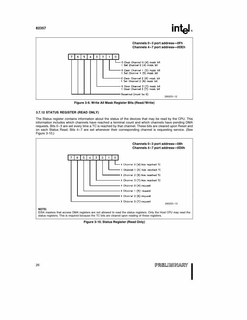
Channels 4–7 port addressÐ0DEh
290253–12
Figure 3-9. Write All Mask Register Bits (Read/Write)
3.7.12 STATUS REGISTER (READ ONLY)
The Status register contains information about the status of the devices that may be read by the CPU. Thisinformation includes which channels have reached a terminal count and which channels have pending DMArequests. Bits 0–3 are set every time a TC is reached by that channel. These bits are cleared upon Reset andon each Status Read. Bits 4–7 are set whenever their corresponding channel is requesting service. (SeeFigure 3-10.)
Channels 0–3 port addressÐ08h
Channels 4–7 port addressÐ0D0h
290253–13
NOTE:EISA masters that access DMA registers are not allowed to read the status registers. Only the Host CPU may read thestatus registers. This is required because the TC bits are cleared upon reading of these registers.
Figure 3-10. Status Register (Read Only)
26
82357
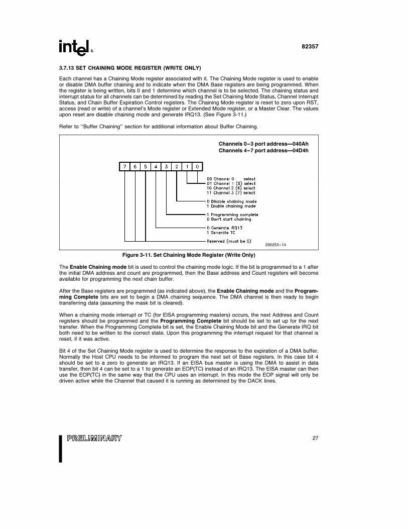
3.7.13 SET CHAINING MODE REGISTER (WRITE ONLY)
Each channel has a Chaining Mode register associated with it. The Chaining Mode register is used to enableor disable DMA buffer chaining and to indicate when the DMA Base registers are being programmed. Whenthe register is being written, bits 0 and 1 determine which channel is to be selected. The chaining status andinterrupt status for all channels can be determined by reading the Set Chaining Mode Status, Channel InterruptStatus, and Chain Buffer Expiration Control registers. The Chaining Mode register is reset to zero upon RST,access (read or write) of a channel’s Mode register or Extended Mode register, or a Master Clear. The valuesupon reset are disable chaining mode and generate IRQ13. (See Figure 3-11.)
Refer to ‘‘Buffer Chaining’’ section for additional information about Buffer Chaining.
Channels 0–3 port addressÐ040Ah
Channels 4–7 port addressÐ04D4h
290253–14
Figure 3-11. Set Chaining Mode Register (Write Only)
The Enable Chaining mode bit is used to control the chaining mode logic. If the bit is programmed to a 1 afterthe initial DMA address and count are programmed, then the Base address and Count registers will becomeavailable for programming the next chain buffer.
After the Base registers are programmed (as indicated above), the Enable Chaining mode and the Program-ming Complete bits are set to begin a DMA chaining sequence. The DMA channel is then ready to begintransferring data (assuming the mask bit is cleared).
When a chaining mode interrupt or TC (for EISA programming masters) occurs, the next Address and Countregisters should be programmed and the Programming Complete bit should be set to set up for the nexttransfer. When the Programming Complete bit is set, the Enable Chaining Mode bit and the Generate IRQ bitboth need to be written to the correct state. Upon this programming the interrupt request for that channel isreset, if it was active.
Bit 4 of the Set Chaining Mode register is used to determine the response to the expiration of a DMA buffer.Normally the Host CPU needs to be informed to program the next set of Base registers. In this case bit 4should be set to a zero to generate an IRQ13. If an EISA bus master is using the DMA to assist in datatransfer, then bit 4 can be set to a 1 to generate an EOP(TC) instead of an IRQ13. The EISA master can thenuse the EOP(TC) in the same way that the CPU uses an interrupt. In this mode the EOP signal will only bedriven active while the Channel that caused it is running as determined by the DACK lines.
27
82357
3.7.14 SET CHAINING MODE STATUS REGISTER (READ ONLY)
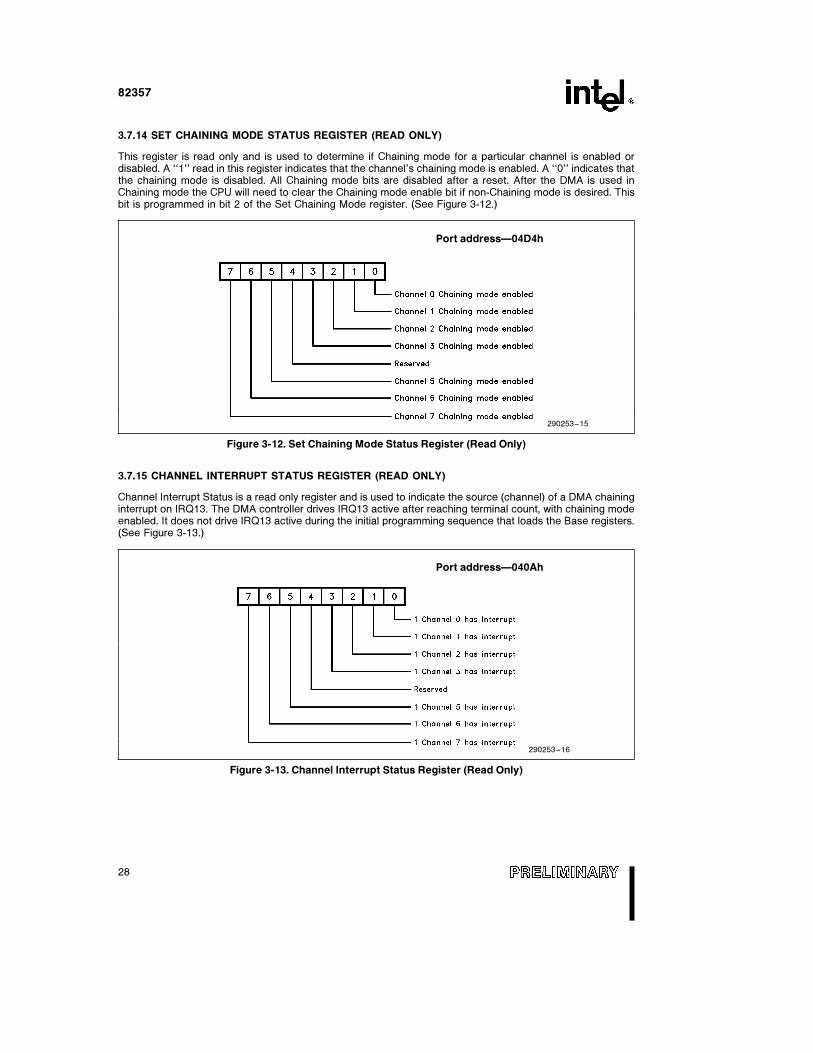
This register is read only and is used to determine if Chaining mode for a particular channel is enabled ordisabled. A ‘‘1’’ read in this register indicates that the channel’s chaining mode is enabled. A ‘‘0’’ indicates thatthe chaining mode is disabled. All Chaining mode bits are disabled after a reset. After the DMA is used inChaining mode the CPU will need to clear the Chaining mode enable bit if non-Chaining mode is desired. Thisbit is programmed in bit 2 of the Set Chaining Mode register. (See Figure 3-12.)
Port addressÐ04D4h
290253–15
Figure 3-12. Set Chaining Mode Status Register (Read Only)
3.7.15 CHANNEL INTERRUPT STATUS REGISTER (READ ONLY)
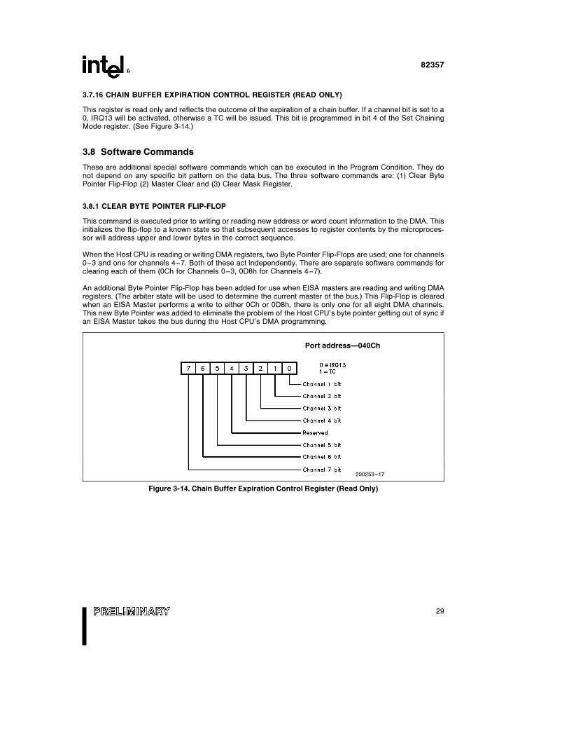
Channel Interrupt Status is a read only register and is used to indicate the source (channel) of a DMA chaininginterrupt on IRQ13. The DMA controller drives IRQ13 active after reaching terminal count, with chaining modeenabled. It does not drive IRQ13 active during the initial programming sequence that loads the Base registers.(See Figure 3-13.)
Port addressÐ040Ah
290253–16
Figure 3-13. Channel Interrupt Status Register (Read Only)
28
82357
3.7.16 CHAIN BUFFER EXPIRATION CONTROL REGISTER (READ ONLY)
This register is read only and reflects the outcome of the expiration of a chain buffer. If a channel bit is set to a0, IRQ13 will be activated, otherwise a TC will be issued. This bit is programmed in bit 4 of the Set ChainingMode register. (See Figure 3-14.)
3.8 Software Commands
These are additional special software commands which can be executed in the Program Condition. They donot depend on any specific bit pattern on the data bus. The three software commands are: (1) Clear BytePointer Flip-Flop (2) Master Clear and (3) Clear Mask Register.
3.8.1 CLEAR BYTE POINTER FLIP-FLOP
This command is executed prior to writing or reading new address or word count information to the DMA. Thisinitializes the flip-flop to a known state so that subsequent accesses to register contents by the microproces-sor will address upper and lower bytes in the correct sequence.
When the Host CPU is reading or writing DMA registers, two Byte Pointer Flip-Flops are used; one for channels0–3 and one for channels 4–7. Both of these act independently. There are separate software commands forclearing each of them (0Ch for Channels 0–3, 0D8h for Channels 4–7).
An additional Byte Pointer Flip-Flop has been added for use when EISA masters are reading and writing DMAregisters. (The arbiter state will be used to determine the current master of the bus.) This Flip-Flop is clearedwhen an EISA Master performs a write to either 0Ch or 0D8h, there is only one for all eight DMA channels.This new Byte Pointer was added to eliminate the problem of the Host CPU’s byte pointer getting out of sync ifan EISA Master takes the bus during the Host CPU’s DMA programming.
Port addressÐ040Ch
290253–17
Figure 3-14. Chain Buffer Expiration Control Register (Read Only)
29
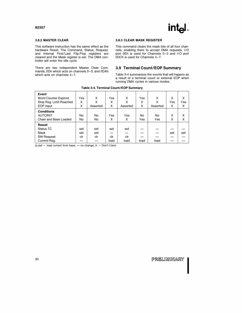
82357
3.8.2 MASTER CLEAR
This software instruction has the same effect as thehardware Reset. The Command, Status, Request,and Internal First/Last Flip-Flop registers arecleared and the Mask register is set. The DMA con-troller will enter the idle cycle.
There are two independent Master Clear Com-mands, 0Dh which acts on channels 0–3, and 0DAhwhich acts on channels 4–7.
3.8.3 CLEAR MASK REGISTER
This command clears the mask bits of all four chan-nels, enabling them to accept DMA requests. I/Oport 0Eh is used for Channels 0–3 and I/O port0DCh is used for Channels 4–7.
3.9 Terminal Count/EOP Summary
Table 3-4 summarizes the events that will happen asa result of a terminal count or external EOP whenrunning DMA cycles in various modes.
Table 3-4. Terminal Count/EOP Summary
Event
Word Counter Expired Yes X Yes X Yes X X X
Stop Reg. Limit Reached X X X X X X Yes Yes
EOP Input X Asserted X Asserted X Asserted X X
Conditions
AUTOINIT No No Yes Yes No No X X
Chain and Base Loaded No No X X Yes Yes X X
Result
Status TC set set set set Ð Ð Ð Ð
Mask set set Ð Ð Ð Ð set set
SW Request clr clr clr clr Ð Ð Ð Ð
Current Reg. Ð Ð load load load load Ð Ð
(Load e load current from base, Ð no change, X e Don’t Care)
30
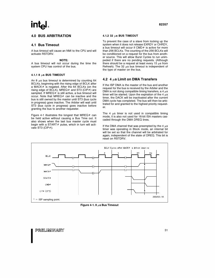
82357
4.0 BUS ARBITRATION
4.1 Bus Timeout
A bus timeout will cause an NMI to the CPU and willactivate RSTDRV.
NOTE:A bus timeout will not occur during the time thesystem CPU has control of the bus.
4.1.1 8 ms BUS TIMEOUT
An 8 ms bus timeout is determined by counting 64BCLKs, beginning with the rising edge of BCLK aftera MACKÝ is negated. After the 64 BCLKs (on therising edge of BCLK), MREQÝ and ST3 (CIPÝ) aresampled. If MREQÝ is still active, a bus timeout willoccur. Note that MREQÝ can be inactive and thebus is still owned by the master until ST3 (bus cyclein progress) goes inactive. The Arbiter will wait untilST3 (bus cycle in progress) goes inactive beforegranting the bus to another requester.
Figure 4-1 illustrates the longest that MREQÝ canbe held active without causing a Bus Time out. Italso shows when the last bus master cycle mustbegin with a STARTÝ pulse, which in turn will acti-vate ST3 (CIPÝ).
4.1.2 32 ms BUS TIMEOUT
To prevent the case of a slave from locking up thesystem when it does not release EXRDY or CHRDY,a bus timeout will occur if CMDÝ is active for morethan 256 BCLKs. The counting of the 256 BCLKs willbe conditioned on a request for the bus from anoth-er source. This will allow Burst Cycles to run unim-peded if there are no pending requests. (Althoughthere should be a request at least every 15 ms fromRefresh). The 32 ms bus timeout is independent ofthe type of master on the bus.
4.2 4 ms Limit on DMA Transfers
If the ISP DMA is the master of the bus and anotherrequest for the bus is received by the Arbiter and theDMA is not doing compatible timing transfers, a 4 mstimer will be started. Upon the expiration of the 4 mstimer, the DACK will be inactivated after the currentDMA cycle has completed. The bus will then be arbi-trated for and granted to the highest priority request-er.
The 4 ms timer is not used in compatible timingmode, it is also not used for 16-bit ISA masters cas-caded through the DMA DREQ lines.
If the DMA channel that was preempted by the 4 mstimer was operating in Block mode, an internal bitwill be set so that the channel will be arbitrated foragain, independent of the state of DREQ. This bit isreset on RSTDRV.
290253–18
* e ISP sampling point.
Figure 4-1. 8 ms Bus Timeout
31

82357
4.3 EISA Bus Master Status Latch
In order to simplify testing of EISA bus master oper-ations, a CPU readable status latch is includedwhich contains information about which EISA busmaster most recently had control of the bus. Thislatch is located at port address 0464h and is readonly. (See Figure 4-2.) A read value of (0) indicatesthat the slot was most recently granted the bus.
An NMI service routine may read this latch to deter-mine which Bus Master controlled the Bus when aBus preempt Timeout occurred.
Port 0465h is reserved for an additional eight BusMaster status latch slots, it is not implemented onthe ISP.
Note that the bits for slot 7 and 8 are driven by theISP, though they will always be inactive (high).
Port 0464h
290253–19
Figure 4-2. EISA Bus Master Status Latch
32
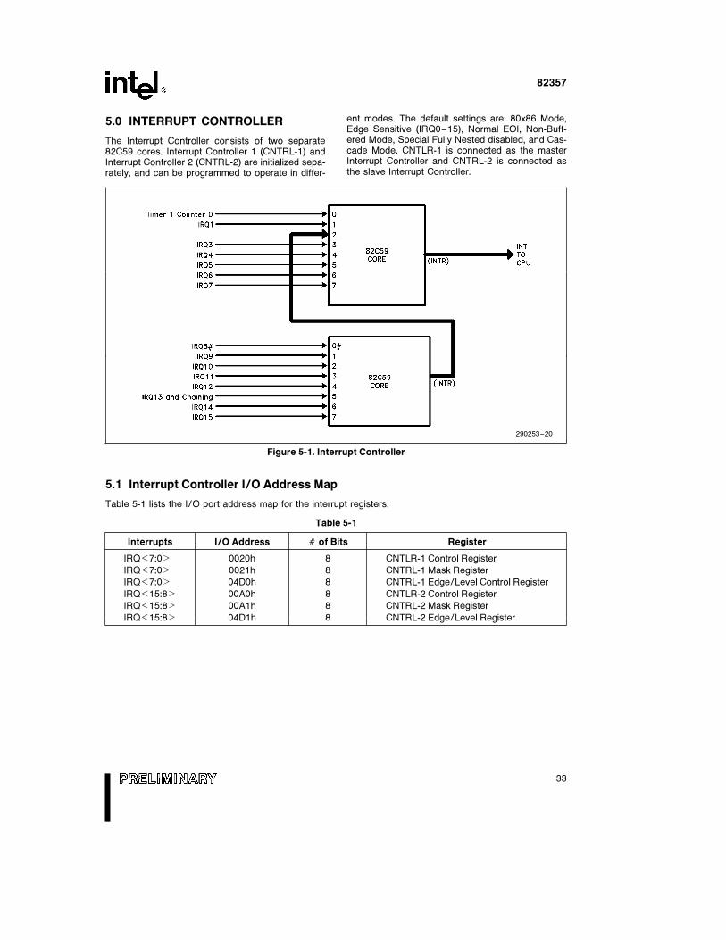
82357
5.0 INTERRUPT CONTROLLER
The Interrupt Controller consists of two separate82C59 cores. Interrupt Controller 1 (CNTRL-1) andInterrupt Controller 2 (CNTRL-2) are initialized sepa-rately, and can be programmed to operate in differ-
ent modes. The default settings are: 80x86 Mode,Edge Sensitive (IRQ0–15), Normal EOI, Non-Buff-ered Mode, Special Fully Nested disabled, and Cas-cade Mode. CNTLR-1 is connected as the masterInterrupt Controller and CNTRL-2 is connected asthe slave Interrupt Controller.
290253–20
Figure 5-1. Interrupt Controller
5.1 Interrupt Controller I/O Address Map
Table 5-1 lists the I/O port address map for the interrupt registers.
Table 5-1
Interrupts I/O Address Ý of Bits Register
IRQk7:0l 0020h 8 CNTLR-1 Control Register
IRQk7:0l 0021h 8 CNTRL-1 Mask Register
IRQk7:0l 04D0h 8 CNTRL-1 Edge/Level Control Register
IRQk15:8l 00A0h 8 CNTLR-2 Control Register
IRQk15:8l 00A1h 8 CNTRL-2 Mask Register
IRQk15:8l 04D1h 8 CNTRL-2 Edge/Level Register
33
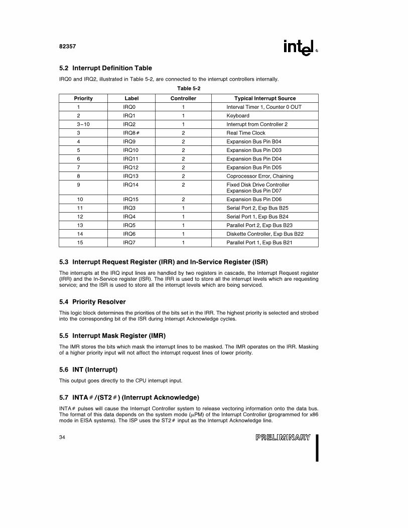
82357
5.2 Interrupt Definition Table
IRQ0 and IRQ2, illustrated in Table 5-2, are connected to the interrupt controllers internally.
Table 5-2
Priority Label Controller Typical Interrupt Source
1 IRQ0 1 Interval Timer 1, Counter 0 OUT
2 IRQ1 1 Keyboard
3–10 IRQ2 1 Interrupt from Controller 2
3 IRQ8Ý 2 Real Time Clock
4 IRQ9 2 Expansion Bus Pin B04
5 IRQ10 2 Expansion Bus Pin D03
6 IRQ11 2 Expansion Bus Pin D04
7 IRQ12 2 Expansion Bus Pin D05
8 IRQ13 2 Coprocessor Error, Chaining
9 IRQ14 2 Fixed Disk Drive ControllerExpansion Bus Pin D07
10 IRQ15 2 Expansion Bus Pin D06
11 IRQ3 1 Serial Port 2, Exp Bus B25
12 IRQ4 1 Serial Port 1, Exp Bus B24
13 IRQ5 1 Parallel Port 2, Exp Bus B23
14 IRQ6 1 Diskette Controller, Exp Bus B22
15 IRQ7 1 Parallel Port 1, Exp Bus B21
5.3 Interrupt Request Register (IRR) and In-Service Register (ISR)
The interrupts at the IRQ input lines are handled by two registers in cascade, the Interrupt Request register(IRR) and the In-Service register (ISR). The IRR is used to store all the interrupt levels which are requestingservice; and the ISR is used to store all the interrupt levels which are being serviced.
5.4 Priority Resolver
This logic block determines the priorities of the bits set in the IRR. The highest priority is selected and strobedinto the corresponding bit of the ISR during Interrupt Acknowledge cycles.
5.5 Interrupt Mask Register (IMR)
The IMR stores the bits which mask the interrupt lines to be masked. The IMR operates on the IRR. Maskingof a higher priority input will not affect the interrupt request lines of lower priority.
5.6 INT (Interrupt)
This output goes directly to the CPU interrupt input.
5.7 INTAÝ/(ST2Ý) (Interrupt Acknowledge)
INTAÝ pulses will cause the Interrupt Controller system to release vectoring information onto the data bus.The format of this data depends on the system mode (mPM) of the Interrupt Controller (programmed for x86mode in EISA systems). The ISP uses the ST2Ý input as the Interrupt Acknowledge line.
34
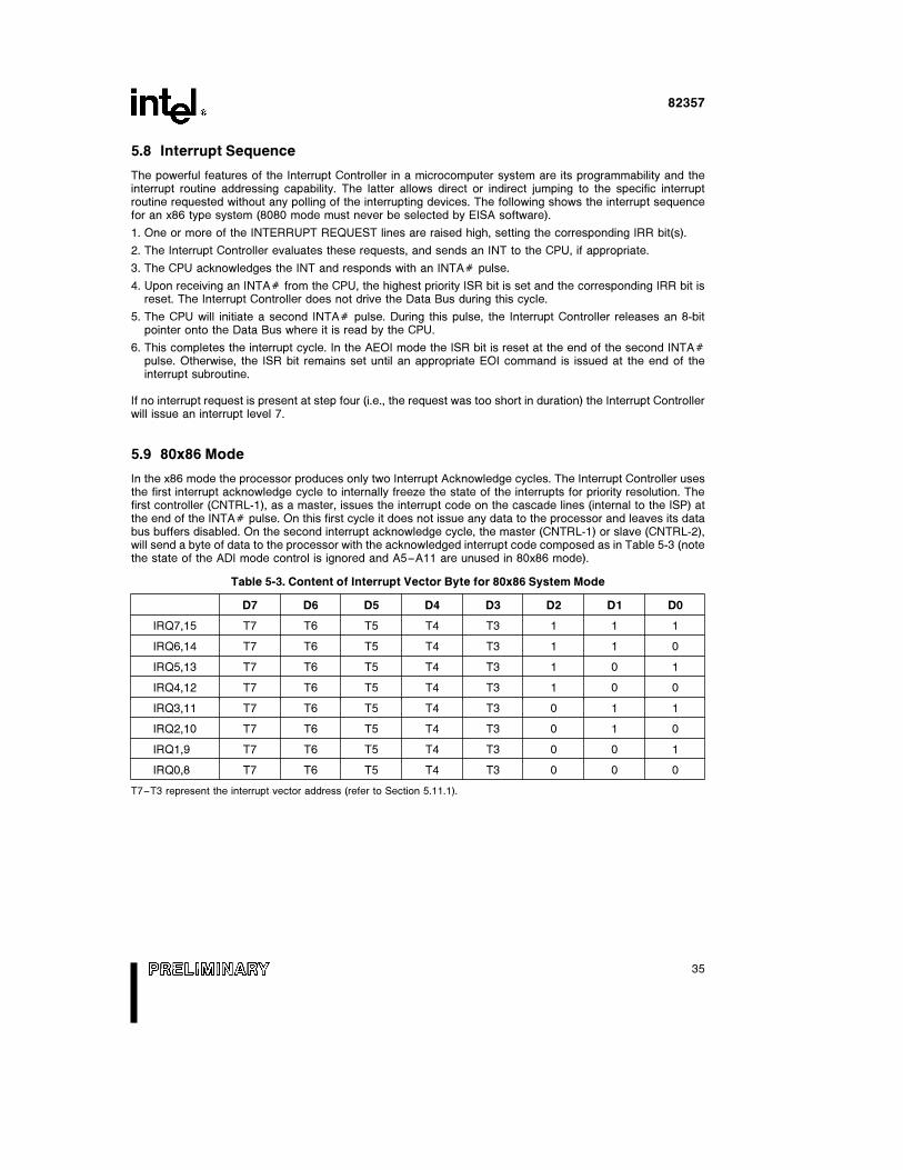
82357
5.8 Interrupt Sequence
The powerful features of the Interrupt Controller in a microcomputer system are its programmability and theinterrupt routine addressing capability. The latter allows direct or indirect jumping to the specific interruptroutine requested without any polling of the interrupting devices. The following shows the interrupt sequencefor an x86 type system (8080 mode must never be selected by EISA software).
1. One or more of the INTERRUPT REQUEST lines are raised high, setting the corresponding IRR bit(s).
2. The Interrupt Controller evaluates these requests, and sends an INT to the CPU, if appropriate.
3. The CPU acknowledges the INT and responds with an INTAÝ pulse.
4. Upon receiving an INTAÝ from the CPU, the highest priority ISR bit is set and the corresponding IRR bit isreset. The Interrupt Controller does not drive the Data Bus during this cycle.
5. The CPU will initiate a second INTAÝ pulse. During this pulse, the Interrupt Controller releases an 8-bitpointer onto the Data Bus where it is read by the CPU.
6. This completes the interrupt cycle. In the AEOI mode the ISR bit is reset at the end of the second INTAÝpulse. Otherwise, the ISR bit remains set until an appropriate EOI command is issued at the end of theinterrupt subroutine.
If no interrupt request is present at step four (i.e., the request was too short in duration) the Interrupt Controllerwill issue an interrupt level 7.
5.9 80x86 Mode
In the x86 mode the processor produces only two Interrupt Acknowledge cycles. The Interrupt Controller usesthe first interrupt acknowledge cycle to internally freeze the state of the interrupts for priority resolution. Thefirst controller (CNTRL-1), as a master, issues the interrupt code on the cascade lines (internal to the ISP) atthe end of the INTAÝ pulse. On this first cycle it does not issue any data to the processor and leaves its databus buffers disabled. On the second interrupt acknowledge cycle, the master (CNTRL-1) or slave (CNTRL-2),will send a byte of data to the processor with the acknowledged interrupt code composed as in Table 5-3 (notethe state of the ADI mode control is ignored and A5–A11 are unused in 80x86 mode).
Table 5-3. Content of Interrupt Vector Byte for 80x86 System Mode
D7 D6 D5 D4 D3 D2 D1 D0
IRQ7,15 T7 T6 T5 T4 T3 1 1 1
IRQ6,14 T7 T6 T5 T4 T3 1 1 0
IRQ5,13 T7 T6 T5 T4 T3 1 0 1
IRQ4,12 T7 T6 T5 T4 T3 1 0 0
IRQ3,11 T7 T6 T5 T4 T3 0 1 1
IRQ2,10 T7 T6 T5 T4 T3 0 1 0
IRQ1,9 T7 T6 T5 T4 T3 0 0 1
IRQ0,8 T7 T6 T5 T4 T3 0 0 0
T7–T3 represent the interrupt vector address (refer to Section 5.11.1).
35

82357
5.10 Programming the Interrupt Controller
The Interrupt Controller accepts two types of command words generated by the CPU or bus master:
1. Initialization Command Words (ICWs): Before normal operation can begin, each Interrupt Controller in thesystem must be brought to a starting pointÐby a sequence of two to four bytes timed by I/O write pulses.
An I/O write to CNTRL-1 or CNTRL-2 base address with D4 e 1 and A0 e 0, is interpreted as ICW1. ForEISA systems, two I/O writes to ‘‘base address a 1’’ must follow the ICW1. The first write to ‘‘base address a
1’’ performs ICW2, the second write performs ICW3. A third write to ‘‘base address a 1’’ performs ICW4. Thebase address for CNTRL-1 is 020h, and the base address for CNTRL-2 is 0A0h.
ICW1 starts the initialization sequence during which the following automatically occur:
a) The edge sense circuit is reset, which means that following initialization, an interrupt request (IRQ) inputmust make a low-to-high transition to generate an interrupt.
b) The Interrupt Mask register is cleared.
c) IR7 input is assigned priority 7.
d) The slave mode address is set to 7.
e) Special Mask Mode is cleared and Status Read is set to IRR.
f) If IC4e0, then all functions selected in ICW4 are set to zero. (Non-Buffered mode*, no Auto-EOI, MCS-80,85 systems).
2. Operation Command Words (OCWs): These are the command words which command the InterruptController to operate in various interrupt modes. These modes are:
a) Fully nested mode
b) Rotating priority mode
c) Special mask mode
d) Polled mode
The OCWs can be written into the Interrupt Controller anytime after initialization.
The Base I/O address for CNTRL-1 is 020h; for CNTRL-2, 0A0h. Table 5-4 lists the initial values set-up atpower-up by the BIOS.
Table 5-4. Initial Interrupt Controller Values
Port Value Description of Contents
020h 11h CNTLR-1, ICW1
021h 08h CNTLR-1, ICW2 Vector Address for 000020h
021h 04h CNTLR-1, ICW3 Indicates Slave Connection
021h 01h CNTLR-1, ICW4 8086 Mode
021h B8h CNTLR-1, Interrupt Mask (may vary)
04D0h 00h CNTRL-1, Edge/Level Control Register
0A0h 11h CNTLR-2, ICW1
0A1h 70h CNTLR-2, ICW2 Vector Address for 0001C0h
0A1h 02h CNTLR-2, ICW3 Indicates Slave ID
0A1h 01h CNTLR-2, ICW4 8086 Mode
04D1h 00h CNTRL-2, Edge/Level Control Register
0A1h BDh CNTLR-2, Interrupt Mask (may vary)
36
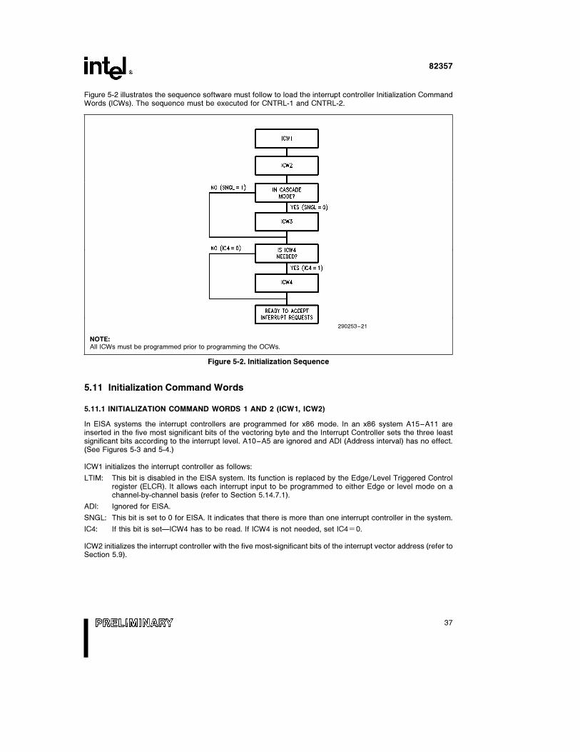
82357
Figure 5-2 illustrates the sequence software must follow to load the interrupt controller Initialization CommandWords (ICWs). The sequence must be executed for CNTRL-1 and CNTRL-2.
290253–21
NOTE:All ICWs must be programmed prior to programming the OCWs.
Figure 5-2. Initialization Sequence
5.11 Initialization Command Words
5.11.1 INITIALIZATION COMMAND WORDS 1 AND 2 (ICW1, ICW2)
In EISA systems the interrupt controllers are programmed for x86 mode. In an x86 system A15–A11 areinserted in the five most significant bits of the vectoring byte and the Interrupt Controller sets the three leastsignificant bits according to the interrupt level. A10–A5 are ignored and ADI (Address interval) has no effect.(See Figures 5-3 and 5-4.)
ICW1 initializes the interrupt controller as follows:
LTIM: This bit is disabled in the EISA system. Its function is replaced by the Edge/Level Triggered Controlregister (ELCR). It allows each interrupt input to be programmed to either Edge or level mode on achannel-by-channel basis (refer to Section 5.14.7.1).
ADI: Ignored for EISA.
SNGL: This bit is set to 0 for EISA. It indicates that there is more than one interrupt controller in the system.
IC4: If this bit is setÐICW4 has to be read. If ICW4 is not needed, set IC4e0.
ICW2 initializes the interrupt controller with the five most-significant bits of the interrupt vector address (refer toSection 5.9).
37
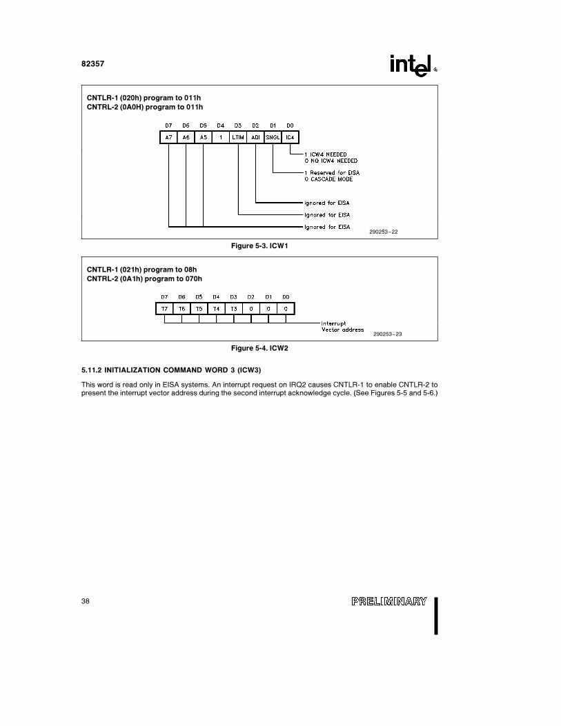
82357
CNTLR-1 (020h) program to 011h
CNTRL-2 (0A0H) program to 011h
290253–22
Figure 5-3. ICW1
CNTLR-1 (021h) program to 08h
CNTRL-2 (0A1h) program to 070h
290253–23
Figure 5-4. ICW2
5.11.2 INITIALIZATION COMMAND WORD 3 (ICW3)
This word is read only in EISA systems. An interrupt request on IRQ2 causes CNTLR-1 to enable CNTLR-2 topresent the interrupt vector address during the second interrupt acknowledge cycle. (See Figures 5-5 and 5-6.)
38
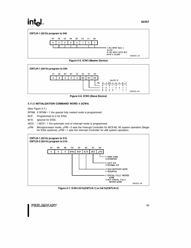
82357
CNTLR-1 (021h) program to 04h
290253–24
Figure 5-5. ICW3 (Master Device)
CNTLR-1 (0A1h) program to 02h
290253–25
Figure 5-6. ICW3 (Slave Device)
5.11.3 INITIALIZATION COMMAND WORD 4 (ICW4)
(See Figure 5-7.)
SFNM: If SFNMe1 the special fully nested mode is programmed.
BUF: Programmed to 0 for EISA.
M/S: Ignored for EISA.
AEOI: I AEOIe1 the automatic end of interrupt mode is programmed.
mPM: Microprocessor mode: mPMe0 sets the Interrupt Controller for MCS-80, 85 system operation (illegalfor EISA systems), mPMe1 sets the Interrupt Controller for x86 system operation.
CNTLR-1 (021h) program to 01h
CNTLR-2 (0A1h) program to 01h
290253–26
Figure 5-7. ICW4 021h(CNTLR-1) or 0A1h(CNTLR-2)
39

82357
5.12 Operation Control Words (OCWs)
After the Initialization Command Words (ICWs) are programmed into the Interrupt Controller, the chip is readyto accept interrupt requests at its input lines. However, during the Interrupt Controller operation, a selection ofalgorithms can command the Interrupt Controller to operate in various modes through the Operation Com-mand Words (OCWs).
5.12.1 OPERATION CONTROL WORD 1 (OCW1)ÐREAD/WRITE
OCW1 sets and clears the mask bits in the interrupt Mask register (IMR). M7–M0 represent the eight maskbits. Me1 indicates the channel is masked (inhibited), Me0 indicates the channel is enabled. (See Figure5-8.)
IRQk7:0lÐPort 021h (CNTRL-1)
IRQk15:0lÐPort 0A1h (CNTRL-2)
290253–27
NOTE:M0eMask for IRQ0(IRQ8Ý), M1eMask for IRQ1(IRQ9), M2eMask for IRQ2(IRQ10) and so on . . .
Figure 5-8. OCW1
5.12.2 OPERATION CONTROL WORD 2 (OCW2)
R, SL, EOIÐThese three bits control the Rotate and End of Interrupt modes and combinations of the two. Achart of these combinations can be found on the Operation Command Word Format.
L2, L1, L0ÐThese bits determine the interrupt level acted upon when the SL bit is active. (See Figure 5-9.)
IRQk7:0lÐPort 020h (CNTRL-1)
IRQk15:0lÐPort 0A0h (CNTRL-2)
290253–28*L0–L2 are used
Figure 5-9. OCW2
40
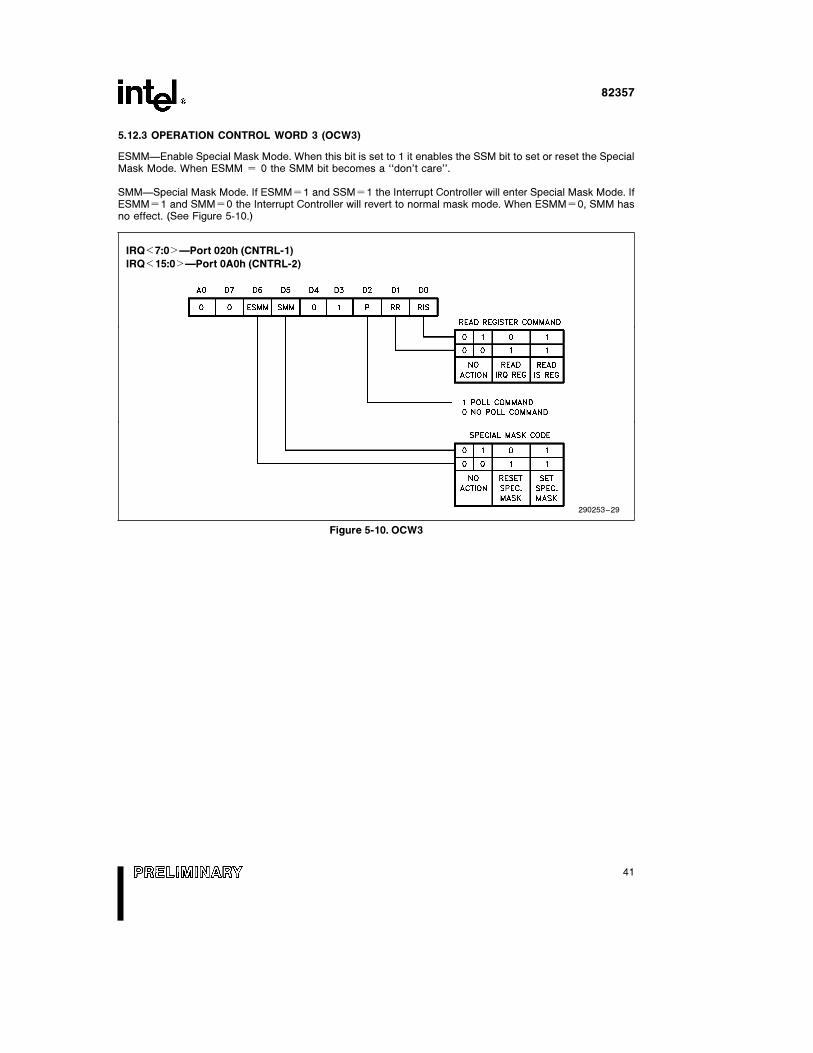
82357
5.12.3 OPERATION CONTROL WORD 3 (OCW3)
ESMMÐEnable Special Mask Mode. When this bit is set to 1 it enables the SSM bit to set or reset the SpecialMask Mode. When ESMM e 0 the SMM bit becomes a ‘‘don’t care’’.
SMMÐSpecial Mask Mode. If ESMMe1 and SSMe1 the Interrupt Controller will enter Special Mask Mode. IfESMMe1 and SMMe0 the Interrupt Controller will revert to normal mask mode. When ESMMe0, SMM hasno effect. (See Figure 5-10.)
IRQk7:0lÐPort 020h (CNTRL-1)
IRQk15:0lÐPort 0A0h (CNTRL-2)
290253–29
Figure 5-10. OCW3
41
82357
5.13 End-Of-Interrupt Operation
5.13.1 END OF INTERRUPT (EOI)
The In Service (IS) bit can be reset either automati-cally following the trailing edge of the last in se-quence INTAÝ pulse (when AEOI bit in ICW1 is set)or by a command word that must be issued to theInterrupt Controller before returning from a serviceroutine (EOI command). An EOI command must beissued twice if the Cascade mode, once for the mas-ter and once for the slave.
There are two forms of EOI commands: Specific andNon-Specific. When the Interrupt Controller is oper-ated in modes which preserve the fully nested struc-ture, it can determine which IS bit to reset on EOI.When a Non-Specific EOI command is issued theInterrupt Controller will automatically reset the high-est IS bit of those that are set, since in the fullynested mode the highest IS level was necessarilythe last level acknowledged and serviced. A non-specific EOI can be issued with OCW2 (EOIe1,SLe0, Re0).
When a mode is used which may disturb the fullynested structure, the Interrupt Controller may nolonger be able to determine the last level acknowl-edged. In this case a Specific End of Interrupt mustbe issued which includes as part of the commandthe IS level to be reset. A specific EOI can be issuedwith OCW2 (EOIe1, SLe1, Re0, and L0–L2 is thebinary level of the IS bit to be reset).
It should be noted that an IS bit that is masked by anIMR bit will not be cleared by a non-specific EOI ifthe Interrupt Controller is in the Special Mask Mode.
5.13.2 AUTOMATIC END OF INTERRUPT(AEOI) MODE
If AEOIe1 in ICW4, then the Interrupt Controller willoperate in AEOI mode continuously until repro-grammed by ICW4. In this mode the Interrupt Con-troller will automatically perform a non-specific EOIoperation at the trailing edge of the last interrupt ac-knowledge pulse. Note that from a system stand-point, this mode should be used only when a nestedmultilevel interrupt structure is not required within asingle Interrupt Controller. The AEOI mode can onlybe used in a master Interrupt Controller and not aslave.
5.14 Modes of Operation
5.14.1 FULLY NESTED MODE
This mode is entered after initialization unless anoth-er mode is programmed. The interrupt requests areordered in priority from 0 through 7 (0 highest).When an interrupt is acknowledged the highest pri-ority request is determined and its vector placed onthe bus. Additionally, a bit of the Interrupt Serviceregister (IS0–7) is set. This bit remains set until themicroprocessor issues an End of Interrupt (EOI)command immediately before returning from theservice routine, or if AEOI (Automatic End of Inter-rupt) bit is set, until the trailing edge of the lastINTAÝ. While the IS bit is set, all further interrupts ofthe same or lower priority are inhibited, while higherlevels will generate an interrupt (which will be ac-knowledged only if the microprocessor internal Inter-rupt enable flip-flop has been re-enabled throughsoftware).
After the initialization sequence, IRQ0 has the high-est priority and IRQ7 the lowest. Priorities can bechanged, as will be explained, in the rotating prioritymode.
5.14.2 THE SPECIAL FULLY NESTED MODE
This mode will be used in the case of a big systemwhere cascading is used, and the priority has to beconserved within each slave. In this case the fullynested mode will be programmed to the master (us-ing ICW4). This mode is similar to the normal nestedmode with the following exceptions:
a) When an interrupt request from a certain slave isin service this slave is not locked out from themaster’s priority logic and further interrupt re-quests from higher priority IRQ’s within the slavewill be recognized by the master and will initiateinterrupts to the processor. (In the normal nestedmode a slave is masked out when its request is inservice and no higher requests from the sameslave can be serviced.)
b) When exiting the Interrupt Service routine thesoftware has to check whether the interrupt serv-iced was the only one from that slave. This isdone by sending a non-specific End of Interrupt(EOI) command to the slave and then reading itsIn-Service register and checking for zero. If it isempty, a non-specific EOI can be sent to the mas-ter too. If not, no EOI should be sent.
42

82357
5.14.3 AUTOMATIC ROTATION(EQUAL PRIORITY DEVICES)
In some applications there are a number of interrupt-ing devices of equal priority. In this mode a device,after being serviced, receives the lowest priority, soa device requesting an interrupt will have to wait, inthe worst case until each of seven other devices areserviced at most once. (See Figure 5-11.)
There are two ways to accomplish Automatic Rota-tion using OCW2, the Rotation on Non-Specific EOICommand (Re1, SLe0, EOIe1) and the Rotate inAutomatic EOI Mode which is set by (Re1, SLe0,EOIe0) and cleared by (Re0, SLe0, EOIe0).
5.14.4 SPECIFIC ROTATION(SPECIFIC PRIORITY)
The programmer can change priorities by program-ming the bottom priority and thus fixing all other pri-orities; i.e., if IRQ5 is programmed as the bottompriority device, then IRQ6 will have the highest one.
The Set Priority command is issued in OCW2 where:Re1, SLe1; L0–L2 is the binary priority level codeof the bottom priority device.
Observe that in this mode internal status is updatedby software control during OCW2. However, it is in-dependent of the End of Interrupt (EOI) command(also executed by OCW2). Priority changes can beexecuted during an EOI command by using the Ro-tate on Specific EOI command in OCW2 (Re1,SLe1, EOIe1 and L0–L2eIRQ level to receivebottom priority).
5.14.5 POLL COMMAND
In this mode the INT output is not used and the mi-croprocessor internal Interrupt Enable flip-flop is re-set, disabling its interrupt input. Service to devices isachieved by software using a Poll command.
The Poll command is issued by setting Pe‘‘1’’ inOCW3. The Interrupt Controller treats the next I/Oread pulse to the Interrupt Controller as an interruptacknowledge, sets the appropriate IS bit if there is arequest, and reads the priority level. Interrupt is fro-zen from the I/O write to the I/O read.
If the priority and ‘‘in service’’ status is:
Before Rotate (IRQ4 the highest priority requiring service)
290253–30
After Rotate (IRQ4 was serviced, all other priorities rotated correspondingly)
290253–31
Figure 5-11
43

82357
The word enabled onto the data bus during I/O readis:
290253–32
W0–W2: Binary code of the highest priority level re-questing service.
1: Equal to ‘‘1’’ if there is an interrupt.
This mode is useful if there is a routine commandcommon to several levels so that the INTAÝ se-quence is not needed (saves ROM space).
5.14.6 CASCADE MODE
The Interrupt Controllers in the EISA system are in-terconnected in a system of one master with oneslave to handle up to 15 priority levels.
In a cascade configuration, the slave interrupt out-puts are connected to the master interrupt requestinputs. When a slave request line is activated andafterwards acknowledged, the master will enable thecorresponding slave to release the device routineaddress during byte 2 of INTAÝ.
Each Interrupt Controller in the system must follow aseparate initialization sequence and can be pro-grammed to work in a different mode. An EOI com-mand must be issued twice: one for the master andonce for the slave.
5.14.7 EDGE AND LEVEL TRIGGERED MODES
In ISA systems this mode is programmed using bit 3in ICW1. In EISA systems the LTIM bit is disabledand a new register for level and edge triggeredmode selection, per interrupt input, is included. Thisis the Edge/Level Control register ELCR. The de-fault programming is equivalent to programming theLTIM bit (ICW1 bit 3) to a 0.
If an ELCR bit e ‘‘0’’, an interrupt request will berecognized by a low to high transition on the corre-sponding IRQ input. The IRQ input can remain highwithout generating another interrupt.
If an ELCR bit e ‘‘1’’, an interrupt request will berecognized by a ‘‘low’’ level on the correspondingIRQ input, and there is no need for an edge detec-tion. For level triggered interrupt mode, the interruptrequest signal must be removed before the EOIcommand is issued or the CPU interrupt must bedisabled. This is necessary to prevent a second in-terrupt from occurring.
In both the edge and level triggered modes the IRQinputs must remain active until after the falling edgeof the first INTAÝ. If the IRQ input goes inactivebefore this time a DEFAULT IRQ7 will occur whenthe CPU acknowledges the interrupt. This can be auseful safeguard for detecting interrupts caused byspurious noise glitches on the IRQ inputs. To imple-ment this feature the IRQ7 routine is used for ‘‘cleanup’’ simply executing a return instruction, thus ignor-ing the interrupt. If IRQ7 is needed for other purpos-es a default IRQ7 can still be detected by readingthe ISR. A normal IRQ7 interrupt will set the corre-sponding ISR bit, a default IRQ7 won’t. If a defaultIRQ7 routine occurs during a normal IRQ7 routine,however, the ISR will remain set. In this case it isnecessary to keep track of whether or not the IRQ7routine was previously entered. If another IRQ7 oc-curs it is a default.
5.14.7.1 Edge/Level Triggered Control Register(ELCR) (Read/Write)
There are two ELCR registers one for each 82C59bank. They are located at I/O ports 04D0h (for theMaster Bank, IRQk0:1,3:7l) and 04D1h (for theSlave Bank, IRQk8Ý:15l). They allow the edgeand level sense selection to be made on an interruptby interrupt basis instead of on a complete bank.Only the interrupts that connect to the EISA bus maybe programmed for level sensitivity. That is IRQ(0, 1, 2, 8Ý, 13) must be programmed for edge sen-sitive operation. (See Figure 5-12.)
IRQ13 still appears externally to be an edge sensi-tive interrupt even though it is shared internally withthe Chaining interrupt. The Chaining interrupt is‘‘ORed’’ after the edge sense logic.
44
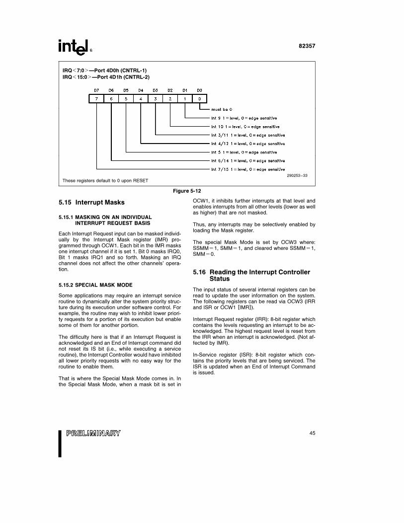
82357
IRQk7:0lÐPort 4D0h (CNTRL-1)
IRQk15:0lÐPort 4D1h (CNTRL-2)
290253–33
These registers default to 0 upon RESET
Figure 5-12
5.15 Interrupt Masks
5.15.1 MASKING ON AN INDIVIDUALINTERRUPT REQUEST BASIS
Each Interrupt Request input can be masked individ-ually by the Interrupt Mask register (IMR) pro-grammed through OCW1. Each bit in the IMR masksone interrupt channel if it is set 1. Bit 0 masks IRQ0,Bit 1 masks IRQ1 and so forth. Masking an IRQchannel does not affect the other channels’ opera-tion.
5.15.2 SPECIAL MASK MODE
Some applications may require an interrupt serviceroutine to dynamically alter the system priority struc-ture during its execution under software control. Forexample, the routine may wish to inhibit lower priori-ty requests for a portion of its execution but enablesome of them for another portion.
The difficulty here is that if an Interrupt Request isacknowledged and an End of Interrupt command didnot reset its IS bit (i.e., while executing a serviceroutine), the Interrupt Controller would have inhibitedall lower priority requests with no easy way for theroutine to enable them.
That is where the Special Mask Mode comes in. Inthe Special Mask Mode, when a mask bit is set in
OCW1, it inhibits further interrupts at that level andenables interrupts from all other levels (lower as wellas higher) that are not masked.
Thus, any interrupts may be selectively enabled byloading the Mask register.
The special Mask Mode is set by OCW3 where:SSMMe1, SMMe1, and cleared where SSMMe1,SMMe0.
5.16 Reading the Interrupt ControllerStatus
The input status of several internal registers can beread to update the user information on the system.The following registers can be read via OCW3 (IRRand ISR or OCW1 [IMR]).
Interrupt Request register (IRR): 8-bit register whichcontains the levels requesting an interrupt to be ac-knowledged. The highest request level is reset fromthe IRR when an interrupt is acknowledged. (Not af-fected by IMR).
In-Service register (ISR): 8-bit register which con-tains the priority levels that are being serviced. TheISR is updated when an End of Interrupt Commandis issued.
45
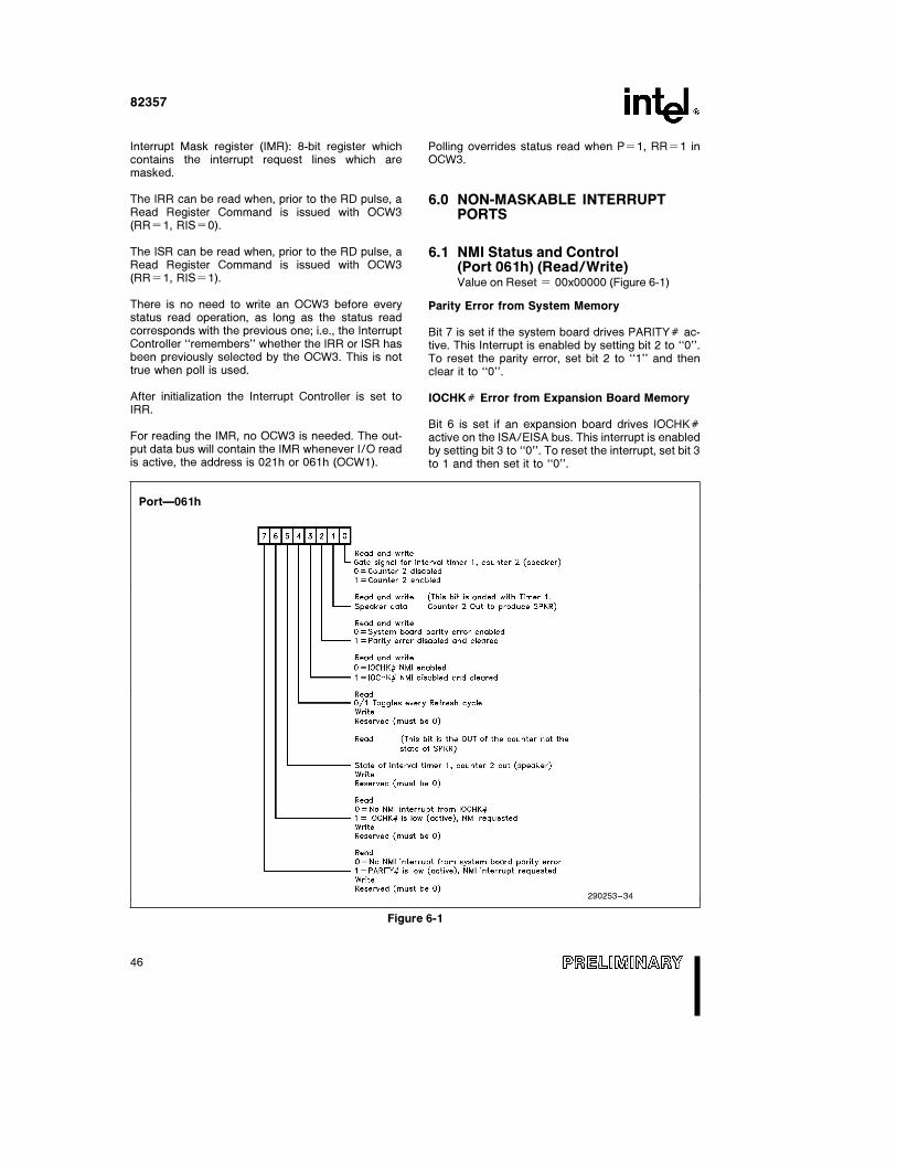
82357
Interrupt Mask register (IMR): 8-bit register whichcontains the interrupt request lines which aremasked.
The IRR can be read when, prior to the RD pulse, aRead Register Command is issued with OCW3(RRe1, RISe0).
The ISR can be read when, prior to the RD pulse, aRead Register Command is issued with OCW3(RRe1, RISe1).
There is no need to write an OCW3 before everystatus read operation, as long as the status readcorresponds with the previous one; i.e., the InterruptController ‘‘remembers’’ whether the IRR or ISR hasbeen previously selected by the OCW3. This is nottrue when poll is used.
After initialization the Interrupt Controller is set toIRR.
For reading the IMR, no OCW3 is needed. The out-put data bus will contain the IMR whenever I/O readis active, the address is 021h or 061h (OCW1).
Polling overrides status read when Pe1, RRe1 inOCW3.
6.0 NON-MASKABLE INTERRUPTPORTS
6.1 NMI Status and Control(Port 061h) (Read/Write)Value on Reset e 00x00000 (Figure 6-1)
Parity Error from System Memory
Bit 7 is set if the system board drives PARITYÝ ac-tive. This Interrupt is enabled by setting bit 2 to ‘‘0’’.To reset the parity error, set bit 2 to ‘‘1’’ and thenclear it to ‘‘0’’.
IOCHKÝ Error from Expansion Board Memory
Bit 6 is set if an expansion board drives IOCHKÝactive on the ISA/EISA bus. This interrupt is enabledby setting bit 3 to ‘‘0’’. To reset the interrupt, set bit 3to 1 and then set it to ‘‘0’’.
PortÐ061h
290253–34
Figure 6-1
46
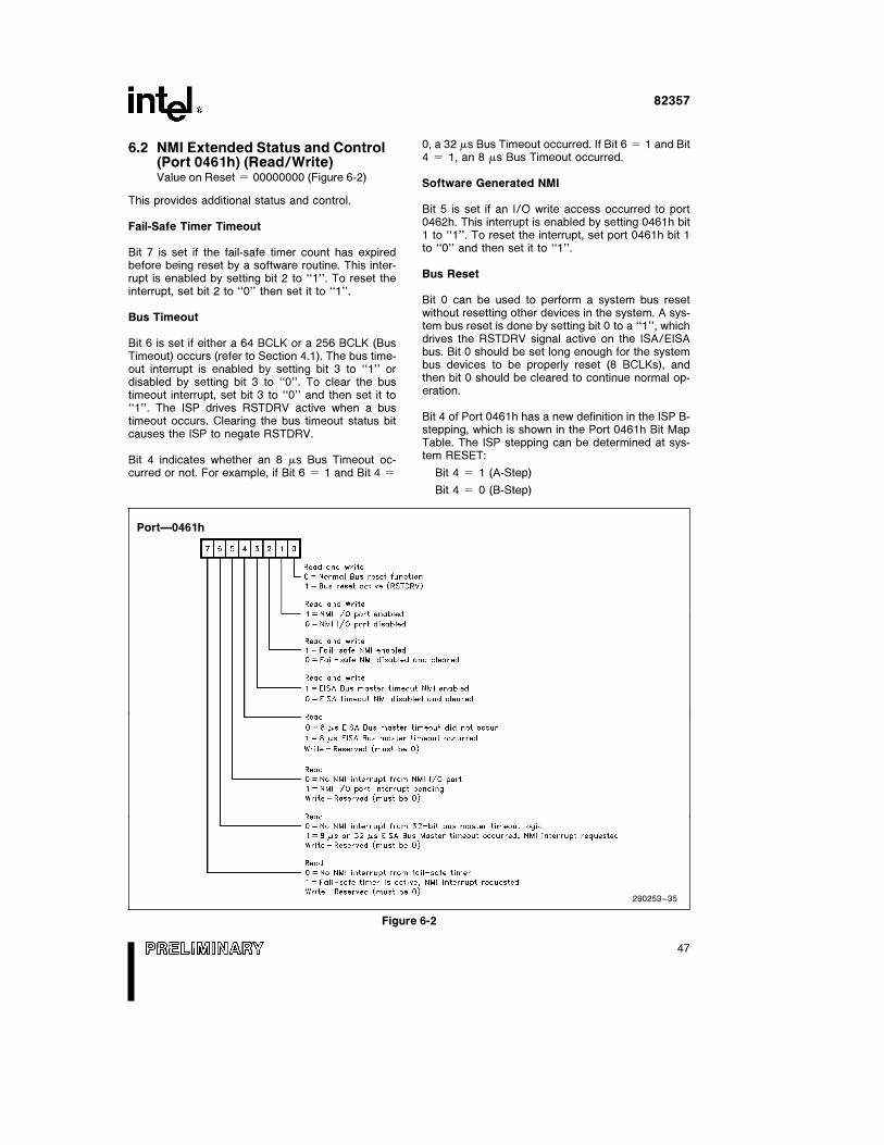
82357
6.2 NMI Extended Status and Control(Port 0461h) (Read/Write)Value on Reset e 00000000 (Figure 6-2)
This provides additional status and control.
Fail-Safe Timer Timeout
Bit 7 is set if the fail-safe timer count has expiredbefore being reset by a software routine. This inter-rupt is enabled by setting bit 2 to ‘‘1’’. To reset theinterrupt, set bit 2 to ‘‘0’’ then set it to ‘‘1’’.
Bus Timeout
Bit 6 is set if either a 64 BCLK or a 256 BCLK (BusTimeout) occurs (refer to Section 4.1). The bus time-out interrupt is enabled by setting bit 3 to ‘‘1’’ ordisabled by setting bit 3 to ‘‘0’’. To clear the bustimeout interrupt, set bit 3 to ‘‘0’’ and then set it to‘‘1’’. The ISP drives RSTDRV active when a bustimeout occurs. Clearing the bus timeout status bitcauses the ISP to negate RSTDRV.
Bit 4 indicates whether an 8 ms Bus Timeout oc-curred or not. For example, if Bit 6 e 1 and Bit 4 e
0, a 32 ms Bus Timeout occurred. If Bit 6 e 1 and Bit4 e 1, an 8 ms Bus Timeout occurred.
Software Generated NMI
Bit 5 is set if an I/O write access occurred to port0462h. This interrupt is enabled by setting 0461h bit1 to ‘‘1’’. To reset the interrupt, set port 0461h bit 1to ‘‘0’’ and then set it to ‘‘1’’.
Bus Reset
Bit 0 can be used to perform a system bus resetwithout resetting other devices in the system. A sys-tem bus reset is done by setting bit 0 to a ‘‘1’’, whichdrives the RSTDRV signal active on the ISA/EISAbus. Bit 0 should be set long enough for the systembus devices to be properly reset (8 BCLKs), andthen bit 0 should be cleared to continue normal op-eration.
Bit 4 of Port 0461h has a new definition in the ISP B-stepping, which is shown in the Port 0461h Bit MapTable. The ISP stepping can be determined at sys-tem RESET:
Bit 4 e 1 (A-Step)
Bit 4 e 0 (B-Step)
PortÐ0461h
290253–35
Figure 6-2
47

82357
6.3 Software NMI Generation(Port 0462h) (Write Only)
A write to this port with any data will cause an NMI.This port provides a software mechanism to causean NMI if interrupts are enabled. (Figure 6-3.)
PortÐ0462
290253–36
Figure 6-3
6.4 NMI Enable/Disable and Real-TimeClock Address (Port 070h)
The Mask register for the NMI interrupt is at I/O ad-dress 070h shown below. The most-significant bitenables or disables all NMI sources includingIOCHKÝ, Fail Safe Timer, PARITYÝ, Bus Time Out,and the NMI Port. Write an 80h to port 70h to maskthe NMI signal. This port is shared with the real-timeclock. The real-time clock uses the lower six bits ofthis port to address memory locations. Writing toport 70h sets both the enable/disable bit and thememory address pointer. Do not modify the contentsof this register without considering the effects on thestate of the other bits. (Figure 6-4.)
PortÐ070h
290253–37
Figure 6-4
7.0 INTERVAL TIMER
EISA systems contain five counter/timers that areequivalent to those found in the 82C54 Programma-ble Interval Timer (NOTE: refer to the 82C54 DataSheet for additional information on timer functions).
The following table shows the I/O address map ofthe interval timer counters:
I/O PortRegister Description
Address
040h Timer 1, System Timer
(Counter 0)
041h Timer 1, Refresh Request
(Counter 1)
042h Timer 1, Speaker Tone
(Counter 2)
043h Timer 1, Control Word
Register
048h Timer 2, Fail-Safe Timer
(Counter 0)
049h Timer 2, Reserved
04Ah Timer 2, CPU Speed Control (Counter 2)
04Bh Timer 2, Control Word
Register
7.1 Programming the Interval Timer
The counter/timers are programmed by I/O access-es and are addressed as though they are containedin two separate 82C54 interval Timers. Timer 1 con-tains three counters, timer 2 contains two counters(EISA systems do not implement the middle counterof timer 2).
The interval timer is an I/O-mapped device. Severalcommands are available:
# Control Word Specifies:
Ð which counter to read or write
Ð the operating mode
Ð the count format (binary or BCD)
# Counter Latch latches the current count so that itcan be read by the system. The countdown pro-cess continues.
# Read Back reads the count value, programmedmode, the current state of the OUT pins, and thestate of the Null Count Flag of the selected coun-ter.
The following Table lists the six operating modes forthe interval counters.
Mode Function
0 Out Signal on End of Count (e0)
1 Hardware retriggerable one-shot
2 Rate Generator (Divide by n Counter)
3 Square Wave Output
4 Software Triggered Strobe
5 Hardware Triggered Strobe
48
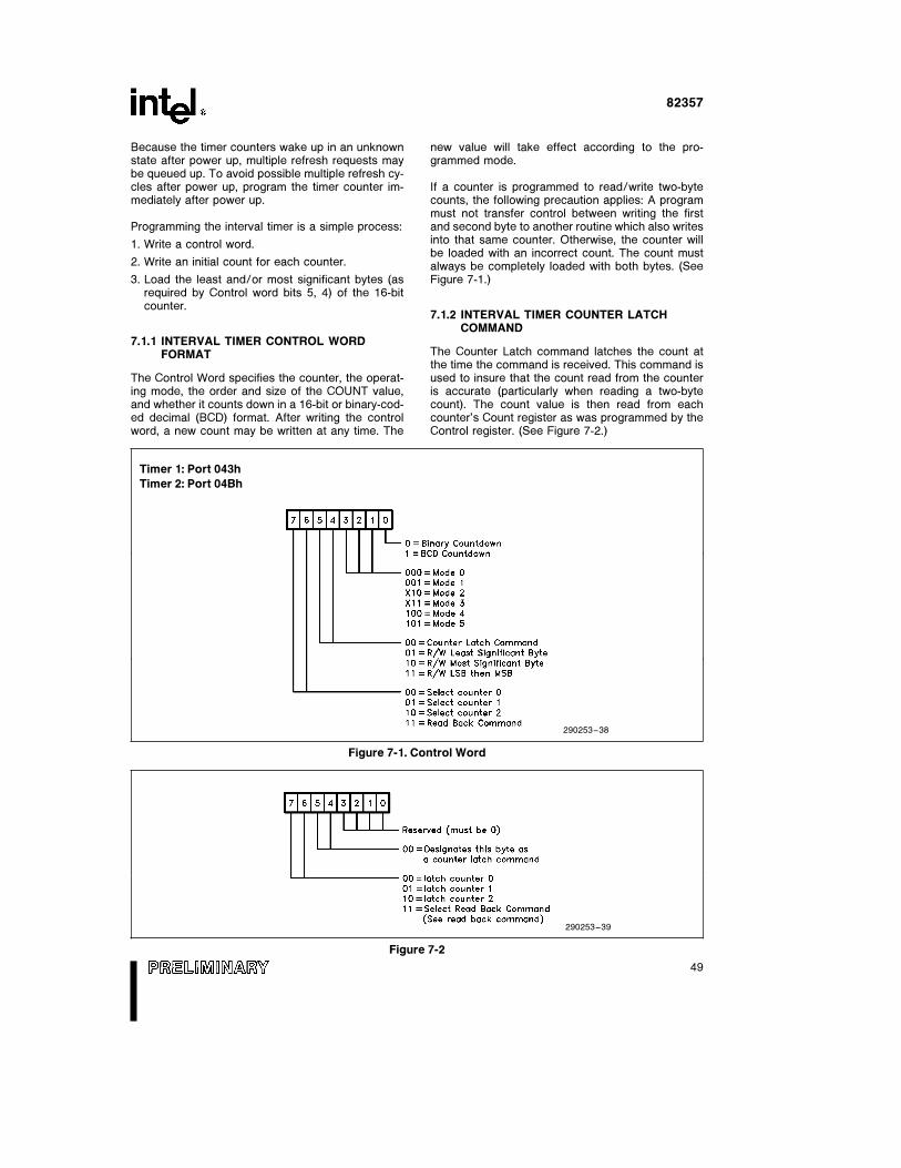
82357
Because the timer counters wake up in an unknownstate after power up, multiple refresh requests maybe queued up. To avoid possible multiple refresh cy-cles after power up, program the timer counter im-mediately after power up.
Programming the interval timer is a simple process:
1. Write a control word.
2. Write an initial count for each counter.
3. Load the least and/or most significant bytes (asrequired by Control word bits 5, 4) of the 16-bitcounter.
7.1.1 INTERVAL TIMER CONTROL WORDFORMAT
The Control Word specifies the counter, the operat-ing mode, the order and size of the COUNT value,and whether it counts down in a 16-bit or binary-cod-ed decimal (BCD) format. After writing the controlword, a new count may be written at any time. The
new value will take effect according to the pro-grammed mode.
If a counter is programmed to read/write two-bytecounts, the following precaution applies: A programmust not transfer control between writing the firstand second byte to another routine which also writesinto that same counter. Otherwise, the counter willbe loaded with an incorrect count. The count mustalways be completely loaded with both bytes. (SeeFigure 7-1.)
7.1.2 INTERVAL TIMER COUNTER LATCHCOMMAND
The Counter Latch command latches the count atthe time the command is received. This command isused to insure that the count read from the counteris accurate (particularly when reading a two-bytecount). The count value is then read from eachcounter’s Count register as was programmed by theControl register. (See Figure 7-2.)
Timer 1: Port 043h
Timer 2: Port 04Bh
290253–38
Figure 7-1. Control Word
290253–39
Figure 7-2
49
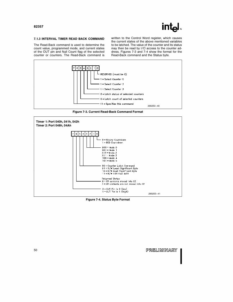
82357
7.1.3 INTERVAL TIMER READ BACK COMMAND
The Read-Back command is used to determine thecount value, programmed mode, and current statesof the OUT pin and Null Count flag of the selectedcounter or counters. The Read-Back command is
written to the Control Word register, which causesthe current states of the above mentioned variablesto be latched. The value of the counter and its statusmay then be read by I/O access to the counter ad-dress. Figures 7-3 and 7-4 show the format for theRead-Back command and the Status byte.
290253–40
Figure 7-3. Current Read-Back Command Format
Timer 1: Port 040h, 041h, 042h
Timer 2: Port 048h, 04Ah
290253–41
Figure 7-4. Status Byte Format
50
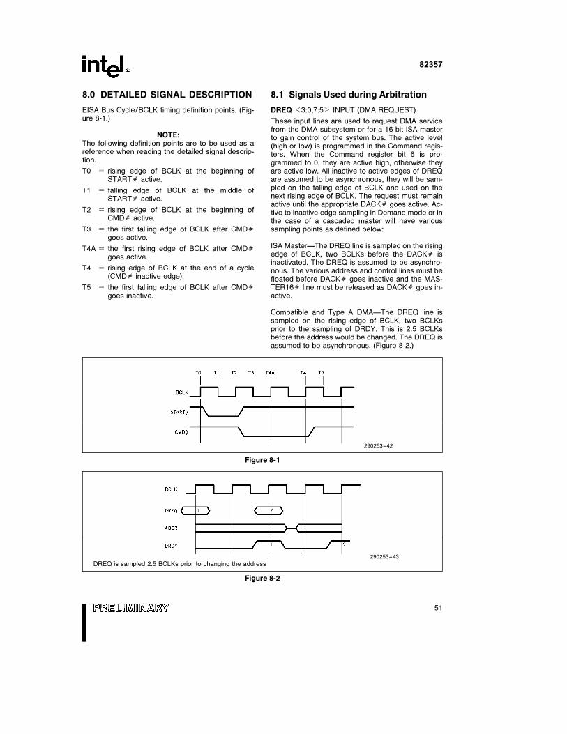
82357
8.0 DETAILED SIGNAL DESCRIPTION
EISA Bus Cycle/BCLK timing definition points. (Fig-ure 8-1.)
NOTE:The following definition points are to be used as areference when reading the detailed signal descrip-tion.
T0 e rising edge of BCLK at the beginning ofSTARTÝ active.
T1 e falling edge of BCLK at the middle ofSTARTÝ active.
T2 e rising edge of BCLK at the beginning ofCMDÝ active.
T3 e the first falling edge of BCLK after CMDÝgoes active.
T4A e the first rising edge of BCLK after CMDÝgoes active.
T4 e rising edge of BCLK at the end of a cycle(CMDÝ inactive edge).
T5 e the first falling edge of BCLK after CMDÝgoes inactive.
8.1 Signals Used during Arbitration
DREQ k3:0,7:5l INPUT (DMA REQUEST)
These input lines are used to request DMA servicefrom the DMA subsystem or for a 16-bit ISA masterto gain control of the system bus. The active level(high or low) is programmed in the Command regis-ters. When the Command register bit 6 is pro-grammed to 0, they are active high, otherwise theyare active low. All inactive to active edges of DREQare assumed to be asynchronous, they will be sam-pled on the falling edge of BCLK and used on thenext rising edge of BCLK. The request must remainactive until the appropriate DACKÝ goes active. Ac-tive to inactive edge sampling in Demand mode or inthe case of a cascaded master will have varioussampling points as defined below:
ISA MasterÐThe DREQ line is sampled on the risingedge of BCLK, two BCLKs before the DACKÝ isinactivated. The DREQ is assumed to be asynchro-nous. The various address and control lines must befloated before DACKÝ goes inactive and the MAS-TER16Ý line must be released as DACKÝ goes in-active.
Compatible and Type A DMAÐThe DREQ line issampled on the rising edge of BCLK, two BCLKsprior to the sampling of DRDY. This is 2.5 BCLKsbefore the address would be changed. The DREQ isassumed to be asynchronous. (Figure 8-2.)
290253–42
Figure 8-1
290253–43
DREQ is sampled 2.5 BCLKs prior to changing the address
Figure 8-2
51
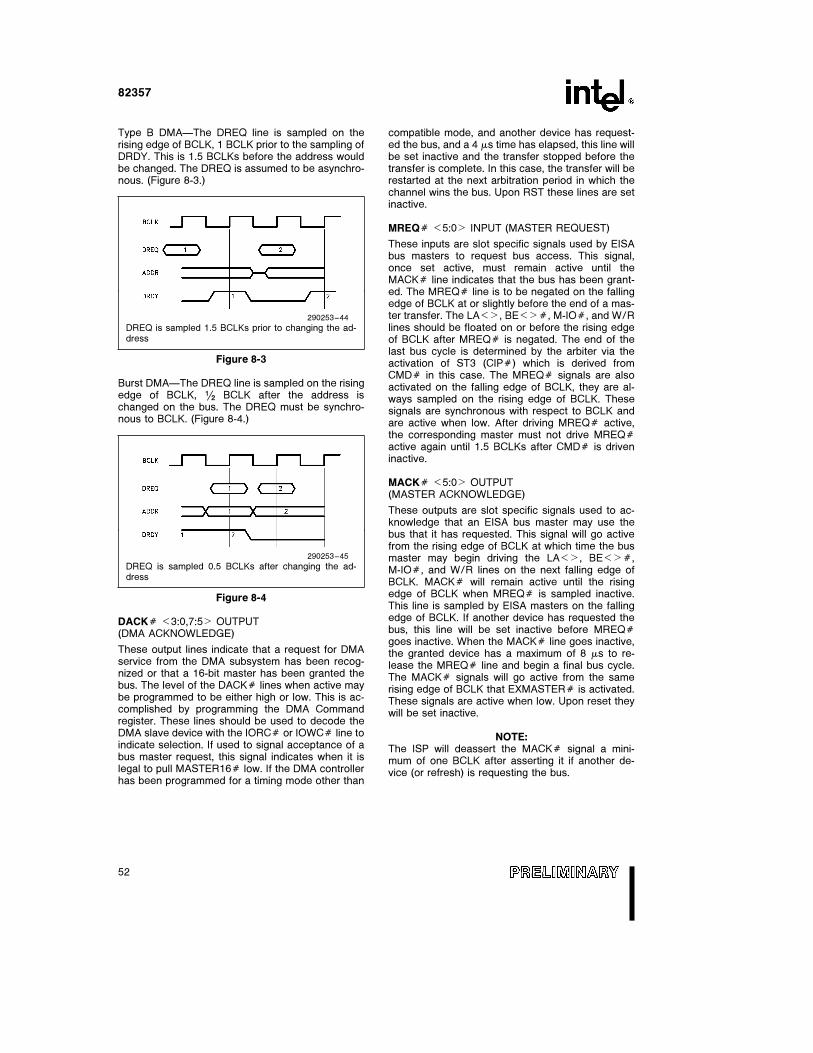
82357
Type B DMAÐThe DREQ line is sampled on therising edge of BCLK, 1 BCLK prior to the sampling ofDRDY. This is 1.5 BCLKs before the address wouldbe changed. The DREQ is assumed to be asynchro-nous. (Figure 8-3.)
290253–44
DREQ is sampled 1.5 BCLKs prior to changing the ad-dress
Figure 8-3
Burst DMAÐThe DREQ line is sampled on the risingedge of BCLK, (/2 BCLK after the address ischanged on the bus. The DREQ must be synchro-nous to BCLK. (Figure 8-4.)
290253–45
DREQ is sampled 0.5 BCLKs after changing the ad-dress
Figure 8-4
DACKÝ k3:0,7:5l OUTPUT(DMA ACKNOWLEDGE)
These output lines indicate that a request for DMAservice from the DMA subsystem has been recog-nized or that a 16-bit master has been granted thebus. The level of the DACKÝ lines when active maybe programmed to be either high or low. This is ac-complished by programming the DMA Commandregister. These lines should be used to decode theDMA slave device with the IORCÝ or IOWCÝ line toindicate selection. If used to signal acceptance of abus master request, this signal indicates when it islegal to pull MASTER16Ý low. If the DMA controllerhas been programmed for a timing mode other than
compatible mode, and another device has request-ed the bus, and a 4 ms time has elapsed, this line willbe set inactive and the transfer stopped before thetransfer is complete. In this case, the transfer will berestarted at the next arbitration period in which thechannel wins the bus. Upon RST these lines are setinactive.
MREQÝ k5:0l INPUT (MASTER REQUEST)
These inputs are slot specific signals used by EISAbus masters to request bus access. This signal,once set active, must remain active until theMACKÝ line indicates that the bus has been grant-ed. The MREQÝ line is to be negated on the fallingedge of BCLK at or slightly before the end of a mas-ter transfer. The LAkl, BEklÝ, M-IOÝ, and W/Rlines should be floated on or before the rising edgeof BCLK after MREQÝ is negated. The end of thelast bus cycle is determined by the arbiter via theactivation of ST3 (CIPÝ) which is derived fromCMDÝ in this case. The MREQÝ signals are alsoactivated on the falling edge of BCLK, they are al-ways sampled on the rising edge of BCLK. Thesesignals are synchronous with respect to BCLK andare active when low. After driving MREQÝ active,the corresponding master must not drive MREQÝactive again until 1.5 BCLKs after CMDÝ is driveninactive.
MACKÝ k5:0l OUTPUT(MASTER ACKNOWLEDGE)
These outputs are slot specific signals used to ac-knowledge that an EISA bus master may use thebus that it has requested. This signal will go activefrom the rising edge of BCLK at which time the busmaster may begin driving the LAkl, BEklÝ,M-IOÝ, and W/R lines on the next falling edge ofBCLK. MACKÝ will remain active until the risingedge of BCLK when MREQÝ is sampled inactive.This line is sampled by EISA masters on the fallingedge of BCLK. If another device has requested thebus, this line will be set inactive before MREQÝgoes inactive. When the MACKÝ line goes inactive,the granted device has a maximum of 8 ms to re-lease the MREQÝ line and begin a final bus cycle.The MACKÝ signals will go active from the samerising edge of BCLK that EXMASTERÝ is activated.These signals are active when low. Upon reset theywill be set inactive.
NOTE:The ISP will deassert the MACKÝ signal a mini-mum of one BCLK after asserting it if another de-vice (or refresh) is requesting the bus.
52

82357
REFRESHÝ I/O OPEN COLLECTOR (REFRESH)
This signal is bidirectional. REFRESHÝ is used asan output during a refresh to indicate that a refreshcycle is in progress. It should be used to enable theSAk15:0l (or LAk15:2l) address to the row ad-dress inputs of all banks of dynamic memory so thatwhen MRDCÝ (or CMDÝ) goes active, the entiresystem memory is refreshed at one time. Memoryslaves must not drive any data onto the bus duringrefresh and should not add wait states since thiswould affect the entire system throughput. As anoutput, this signal is driven directly onto the EISAbus. This signal is an output only when the ISP is amaster on the bus responding to an internally gener-ated request for Refresh. Upon RST this pin will tri-state.
REFRESHÝ may be driven by an expansion busadapter card acting as a 16-bit ISA bus master. Asan input, it is assumed to be asynchronous with re-spect to BCLK. It will be sampled on the falling edgeof BCLK and used on the following rising edge ofBCLK.
DHLDA INPUT (HOLD ACKNOWLEDGE)
This signal indicates that the system has granted theISP arbitration logic the use of the host bus. DHLDAis an asynchronous signal with respect to BCLK. It issampled on the falling edge of BCLK and used onthe next rising edge of BCLK. This signal is activehigh.
CPUMISSÝ INPUT (CPU CACHE MISS)
This signal from the host CPU or Cache controllersubsystem, indicates that a CPU or Cache controllerbus cycle is pending and that the System arbitrationlogic in the ISP should include the CPU as a con-tender in the next bus arbitration. This signal is asyn-chronous with respect to BCLK. It is sampled on thefalling edge of BCLK and used on the next risingedge of BCLK. It is an active low signal. This signalshould not be generated to the ISP when the CPU orcache own the bus (i.e., when HLDA is inactive).
DHOLD OUTPUT (CPU HOLD REQUEST)
This output signal is used to request control of thehost or differentiation bus. In a simple system thiswould be making a request from the CPU, in a sys-tem with a cache, from the cache. This signal is syn-chronized to the requirements of the CPU or cacheby the EBC. Upon RST this pin is set inactive.
EMSTR16Ý OUTPUT (ISA 16-BIT MASTER)
This output signal is used to tell the bus controllerthat an ISA 16-bit master has control of the bus. Thiswill enable the bus controller to do the appropriatetranslation of signals. This signal is driven active 1BCLK prior to the BCLK that the ISA Master DACKÝsignals are driven active, and driven inactive with thesame BCLK that the ISA DACKÝ signals arechanged on. This signal is active low. It is set inac-tive upon RST. EMSTR16Ý from the ISP must beANDed with SPWROK from the EBC to generateEMSTR16Ý to the EBC so that EBC internal signalsare initialized before STARTÝ is driven active in thefirst cycle.
EXMASTERÝ OUTPUT (EISA MASTER)
This output signal is used to tell the bus controllerthat a new EISA bus master, 16- or 32-bit, has con-trol of the bus. This will enable the bus controller todo the appropriate translations of signals. This signalis driven active and inactive with the MACKÝ signalson the rising edge of BCLK except in the case ofPREEMPT. In this case, EXMASTERÝ is negatedon the same rising BCLK edge that CIPÝ (ST3) issampled active. Upon RST this pin is set inactive.
8.2 Signals Used during DMA andRegister Access
STARTÝ INPUT (START OF CYCLE)
This signal is connected directly to the EISASTARTÝ. It is used only in slave mode to indicatethe start of a bus cycle. It is sampled on the risingedge of BCLK.
CMDÝ INPUT (COMMAND)
This signal is connected directly to the EISA CMDÝ.CMDÝ is used in slave mode to determine when totri-state the data buffers after a read cycle. The databuffers will be floated when CMDÝ goes inactive.The leading edge of this signal is always synchro-nous, driven from a rising edge of BCLK. The trailingedge is asynchronous only in the case of an ISA busmaster.
EOP TRI-STATED (END OF PROCESS)
This pin is bidirectional, acting in one of threemodes, and is directly connected to the TC line ofthe ISA/EISA bus. In the first mode, EOPIN, the pinis an input and can be used by a DMA slave to stopa DMA transfer. In the second mode, TCOUT, it is
53

82357
used as a terminal count output by DMA slaves. Anactive pulse is generated when the byte counterreaches its last value. In the third mode, INTOUT, itindicates to an EISA programming master that achaining buffer has been expired and a new chainbuffer should be programmed. The timings are asfollows:
Eopin Mode
During DMA, using Compatible, Type A or Type Btransfers, the EOP pin is sampled by the ISP on therising edge of BCLK preceding the falling edge thataddress is changed. If it is sampled active, the ad-dress is tri-stated on the falling edge of BCLK, andthe transfer is terminated. (Figure 8-5.)
When using Burst cycles, the EOP is sampled at thesame time as the DREQ input, (/2 BCLK after theaddress was changed. (Figure 8-6.)
290253–46
EOP is sampled 0.5 BCLKs prior to changing the ad-dress
Figure 8-5
290253–47
EOP is sampled 0.5 BCLKs after changing the address
Figure 8-6. Burst Mode EOP Timing
Tcout Mode
In this mode the EOP output behaves differently de-pending on whether or not the channel is pro-grammed for Burst mode. If the channel is not pro-grammed for Burst mode, the EOP output will goactive 1.5 BCLKs after a new address has been out-put if the byte count expires with that transfer. Inburst mode, EOP is driven active along with addresssince some transfers may only last 1 BCLK cycle.The EOP (TC) will be active until AENÝ goes inac-tive for both Burst and non-Burst DMA (even afterthe address is tri-stated), except in the following twocases: Case 1ÐEOP (TC) will go inactive four BCLKcycles before AENÝ goes inactive during an Autoini-tialization or Buffer Chaining function. Case 2ÐEOP(TC) will go inactive one BCLK cycle before AENÝgoes inactive if the DMA channel that is currently inuse is configured for Type ‘‘B’’ timing.
Intout Mode
In this mode the EOP signal has the same behavioras the Chaining Interrupt to the host processor(IRQ13). If a chaining buffer is expired, EOP will goactive on the falling edge of BCLK. Only the current-ly active channel’s chaining interrupt will be reflectedon this pin. Other channels with active chaining in-terrupts pending will not affect the EOP pin.
Whenever all the DMA channels are not in use, theEOP pin is kept in output mode and inactive.
BEk3:0lÝ I/O TRI-STATED (BYTE ENABLES)
BEk3:0lÝ are the byte enables of EISA bus.BEk2:0lÝ are bidirectional and BE3Ý is an outputonly. In master mode BEk3:0lÝ are outputs andare translated by the EBC to HBEk3:0lÝ or ISAsignals, whichever are appropriate. In Master modethe ISP will directly drive the EISA bus. The BE linesare always tri-stated on the T3 BCLK. The BE linesare re-enabled by the DMA on the falling edge ofBCLK if DRDY is sampled active on the previousrising edge of BCLK.
54
82357
In slave mode BEk2:0lÝ are used in conjunctionwith HAk15:2l to address the ISP’s internal regis-ters. BEk2:0lÝ are latched on the T2 edge ofBCLK.
HAk31:2l I/O TRI-STATED(HOST ADDRESS BUS)
These signals are Address signals and are connect-ed to the host bus. HAk31:20l and k15:2l arebidirectional, HAk19:16l are output only. In mastermode they are outputs and are used in conjunctionwith BEk3:0lÝ during DMA and Refresh cycles. Inslave mode HAk15:2l and k31:20l are inputs.HAk15:2l in conjunction with BEk2:0lÝ areused to address the internal ISP registers.HAk15:2l are latched with transparent latches bythe trailing (rising) edge of DADSÝ (ST0).HAk31:20l are used to decode GT1MÝ. UponRST these pins are tri-stated and placed in inputMode.
HW/RÝ I/O TRI-STATED (HOST WRITE/READ)
This line is bi-directional and connects to the hostbus. In slave mode HW/RÝ is an input and is usedto indicate a read cycle when low and a write cyclewhen high. When in slave mode, HW/RÝ is latchedwith transparent latches by the trailing (rising) edgeof ST0 (DADSÝ). In master mode this pin is an out-put and will have the same timings as HAk31:2l.As an output, it is used during DMA or Refresh cy-cles by the EBC to propagate the appropriate write/read signals to the EISA Bus. This pin is placed inoutput mode only during DMA or Refresh cycles.Upon RST this pin is tri-stated and placed in inputmode.
GT16MÝ OUTPUT TRI-STATED (l16 MBYTES)
GT16MÝ is directly connected to the EBC and indi-cates that the DMA address on HAkl is greaterthan 00FFFFFF (16 Mbytes). This signal is an outputonly when the DMA is the bus master, it is tri-statedotherwise.
The EBC uses this signal during DMA cycles to de-termine whether or not to generate ISA memorycommand signals. If it is not driven by anothersource, it should be pulled up with an external resis-tor to keep the node, which is an input to the EBC,from floating. This signal has timings similar to theHAk31:2l lines. Upon RST it will be tri-stated.
GT1MÝ OUTPUT (l1 MBYTE)
GT1MÝ is directly connected to the EBC and indi-cates when the address on the HAkl address linesis greater than 000FFFFFh (1 Mbyte). It is decodedby the ISP from the HAk31:20l bus and is used bythe bus controller to control the SMRDCÝ andSMWTCÝ signals. Its timing is a combinatorial delayfrom HAk31:20l in all cycles. Upon RST its statedepends on the state of the address bus.
RST INPUT (SYSTEM RESET)
This signal is connected directly to the EBC and indi-cates that the ISP should initialize all of its registersand state machines as well as driving the RSTDRVoutput active. This signal is asynchronous with re-spect to BCLK and must have a minimum activepulse width for eight BCLKs. 3.5 BCLKs are requiredfrom the inactive edge of RST to the T2 edge of thefirst slave cycle to the ISP.
BCLK INPUT (BUS CLOCK)
This signal is used as the main clock reference forthe ISP and the EISA bus. BCLK is tied directly tothe BCLK output of the EBC. The EBC divides theHost CPU Clock (HCLKCPU) by an appropriate num-ber to generate BCLK. The normal frequency rangeof BCLK is 8.00 MHz to 8.333 MHz with a normalduty cycle of 50%. The high or low time can bestretched by the EBC for synchronization purposes,(REFER TO THE EBC DATA SHEET).
STk3:0l I/O TRI-STATED WITH WEAK PULLUP(DMA STATUS)
These are synchronous bidirectional control signalsbetween the ISP and the EBC. These pins are out-put during DMA and refresh cycles. They indicatewhat type of timing has been programmed for thecurrent cycle and the size of the I/O device involvedin the DMA transfer. The EBC takes ST0–ST3 andgenerates the appropriate command signals for theISP. The command signals generated from ST0–ST3 are used to control the timing of the cycle. Dur-ing cycles where the ISP is in slave mode, these pinsare inputs. All of these pins have weak pullup resis-tors to sustain a high level when neither the EBC orISP are driving the signals. Their definition is as fol-lows:
Master Mode
ST1 ST0 DMA Cycle Timing
0 0 Compatible Cycle Timing
0 1 Type A Timing
1 0 Type B Timing
1 1 Burst Timing
These signals always transition on the falling edgeof BCLK.
ST3 ST2DMA Slave Size or
Idle Indication
0 0 8-Bit
0 1 16-Bit
1 0 32-Bit
1 1 Idle
55
82357
These signals will always go active on the fallingedge of BCLK. They will go inactive on the fallingedge of BCLK after the last DMA transfer, or on therising edge of BCLK if a page break is detected(burst mode) or the transfer is about to end (burstmode).
Slave Mode
ST0 has the DMA address strobe function. This sig-nal is used to latch the address and status informa-tion on the host bus. Specifically the signals latchedwith this signal are HAk15:2l, ST1 (M/IOÝ) andHW/RÝ. These signals have a setup and hold timearound the rising edge of ST0. The leading edge ofST0 also has a setup time to BCLK at T2.
ST1 is the memory or I/O indicator pin (M/IOÝ),1eMemory Cycle, 0eI/O Cycle. This signal islatched by the rising edge of ST0.
ST2 is the Interrupt Acknowledge pin (INTAÝ).When ST2e0, the cycle is an Interrupt Acknowl-edge. When ST2e1, the cycle is not an InterruptAcknowledge. This signal is sampled by the ISP inslave mode at the T2 BCLK edge. It has a setup andhold time with respect to that BCLK edge so it mustnot be pipelined along with the HA lines. Only non-ISA masters can run interrupt acknowledge cycles.Only the host CPU has the control signals to runinterrupt acknowledge cycles. ST2 must be tied highwith a 1.2K pullup resistor.
ST3 is the cycle in progress pin (CIPÝ). This is anindication to the ISP System Arbiter that there is abus cycle in progress. It is used to detect when thebus is free after an EISA master gives it up by drivingMREQÝ inactive. This signal is sampled on risingedges of BCLK.
These pins are output only when the DMA is the busmaster or during Refresh cycles. Upon RST thesepins are tri-stated and placed in input Mode.
DRDY I/O TRI-STATED WITH WEAK PULLUP(READY SIGNAL)
This pin is an output in slave mode and an input inmaster mode. In slave mode it is used by the EBC asan end of cycle indicator and is used to combinatori-ally drive CHRDY. DRDY is actively driven only whenthe ISP detects a slave cycle to one of its registers.At all other times it is sustained in a high state inter-nally by a very weak pullup resistor. It is actively driv-en from the T2 edge of BCLK of an ISP cycle thatrequires more than a two BCLK wide CMDÝ pulsewidth when an ISA device is the bus master. DRDYwill not be driven low when the bus master is either
the host CPU or an EISA master. If DRDY is drivenlow, it will be kept low for four BCLKs after the T2edge of BCLK. It will then be driven high off the ris-ing edge of BCLK. The DRDY output buffer is en-abled at T2 and disabled as a result of an inactiveCMDÝ after T4A. DRDY will be asynchronously dis-abled upon the inactive edge of CMDÝ.
In master mode DRDY is used to indicate to theDMA controller that the current cycle is completed(DMA-READY) and that the DMA controller shouldpipeline addresses for Burst DMA transfers (START-PIPELINING). In master mode, DRDY, is sampled2.5 BCLK periods after STk3:2l are driven to anon-idle state from an idle one. This indicatesSTART-PIPELINING. If DRDY is sampled high atthis point, the DMA controller begins address pipe-lining. Pipelining is stopped at a page break or at theend of a transfer. DRDY is then sampled on the nextBCLK rising edge and on all subsequent BCLK risingedges until STk3:2l go to idle, to determine DMA-READY. If the DMA is pipelining addresses, DRDYwill be sampled until active one last time afterSTk3:2l go to the idle state (to complete the lastDMA cycle). Upon RST this pin is tri-stated and mustbe tied high with a 2.4K pullup resistor.
Dk7:0l I/O TRI-STATED (DATA LINES)
This bidirectional bus is the ISP’s slave mode databus. In master mode the data lines are not used.These pins are output only when CSOUTÝ is activeduring I/O read or Interrupt Acknowledge cycles.That is only when the ISP is being accessed as aresult of an I/O read or Interrupt Acknowledge.These pins are inputs during an I/O write cycle tothe ISP’s internal registers. Upon RST these pinsare tri-stated and placed in input mode.
This bus needs to be externally buffered to provideadequate drive to the EISA bus. In ISP master mode,this bus is not used. Upon RST these pins are tri-stated and placed in input Mode.
CSOUTÝ OUTPUT (SLAVE MODE SELECTED)
This output signal from the ISP indicates when theISP is being accessed in slave mode. CSOUTÝ willgo active from the rising edge of BCLK at T2 after aslave cycle to or from the ISP has been detected. Itwill not be active prior to that, i.e., between T0 andT2. CSOUTÝ is deactivated as a result of an inac-tive edge of CMDÝ, this is done asynchronously.CSOUTÝ will also be active during all interrupt ac-knowledge cycles. CSOUTÝ should be used to con-trol the output enable of an EISA local data bustransceiver. This pin is always an output. Upon Re-set it will be inactive (high).
56
82357
AENÝ OUTPUT (ADDRESS ENABLE)
This output signal, when inactive (high), indicatesthat the CPU or another EISA or ISA bus master hascontrol of the bus. When active (low), the DMA con-troller has control of the bus. AENÝ will also go ac-tive during Refresh cycles. AENÝ is used to disableI/O devices which must not respond during a DMAcycle. This signal is further processed by the systemboard to form the slot specific AENÝ signals. UponRST this pin is set inactive.
8.3 Signals Used during an InterruptSequence
IRQ k15:3,1l INPUT (INTERRUPT REQUEST)
The active polarity of these inputs depends on theprogramming of the two ELCR registers. Only theEISA bus interrupts may be programmed for activelow operation in the ELCR registers, all other inter-rupts will always be edge-triggered. If an interrupt isprogrammed for active low operation and sharedwith open collector drivers, an external pullup willneed to be included to restore the inactive high lev-el. Upon RST, the IRQ lines will be placed in edge-triggered mode.
The IRQ inputs must remain active until after the firstfalling edge of INTA(ST2Ý). If the IRQ input goesinactive before this time, a DEFAULT IR7 will occurwhen the CPU acknowledges the interrupt. (Refer toSection 5.14.7.)
INT OUTPUT (CPU INTERRUPT)
This signal is driven by the ISP’s interrupt controllersubsystem to signal the CPU that an Interrupt re-quest is pending and needs to be serviced. It isasynchronous with respect to BCLK and is alwaysan output. For i486 CPU systems, INT must be exter-nally latched from the ISP until an Interrupt Acknowl-edge cycle occurs. INT will remain active until afterthe first INTA(ST2Ý) pulse. Upon RST the state ofthis pin is undefined.
8.4 Counter/Timer, NMI andMiscellaneous Utility Signals
OSC INPUT (COUNTER CLOCK)
This is a 14.31818 MHz input clock for use by thetimers. This clock is divided by 12 and 48 to form theCLK input on several of the counters. It is asynchro-nous with respect to BCLK.
IOCHKÝ INPUT (I/O CHECK BUS ERROR)
This input signal comes from the ISA bus. It is usedfor parity errors on memory cards plugged into thebus, and for other high priority interrupts. The sys-tem board needs a pullup resistor to keep this signalinactive when it is not being driven active by some
device. The active level of this signal will generatean NMI if this function is enabled in Port 061h. Forexample, if IOCHKÝ is active and Port 061h, bit 3 isset to 1 (inactive) no NMI will be caused, however,when Port 061h bit 3 is set to 0 (active) an NMI willbe caused, providing that the IOCHKÝ input is stillactive and Port 070h bit 7 is enabled (0). This signalis asynchronous with respect to BCLK.
RSTDRV OUTPUT (SYSTEM BUS RESET)
This output signal is used by the EISA bus to disableand reset all installed adapters. More specifically,ISA/EISA bus masters and DMA devices must re-lease and stop requesting the bus until repro-grammed by the system. Any drivers that are con-nected to the system bus must be tri-stated by thissignal. In addition to being activated by RST,RSTDRV can be activated by a write to port 0461hor a bus timeout. A bus timeout will occur if an EISAbus master exceeds its allowable 8 ms time on thebus after being requested to get off by the removalof its MREQÝ. Once the RSTDRV is activated bythe bus timeout, the timed out master will releasethe bus allowing the host CPU to gain control of thesystem. A Bus Timeout will also occur upon thetimeout of the 32 ms CMDÝ active timer. This outputdrives the EISA bus directly and has a 24 mA drivecapability. RSTDRV will remain active as long as thesource of the Bus Reset is active.
NOTE:The 8x42 Keyboard Controller requires clocks(CLKKB) before the end of RSTKBDÝ (keyboardreset pulse) for keyboard reset to occur. To ensurethat RSTKBDÝ has been driven inactive after theEBC has begun generating CLKKB; RSTDRV andRSTCPU are logically NANDed to generateRSTKBDÝ for the 8x42.
PARITYÝ INPUT (PARITY ERROR)
This signal is the main memory parity error inputfrom the system board. The system board reportsany parity errors from its memory system on this line.The active edge of this signal will generate an NMI ifthis function is enabled in Port 061h. For example, ifPARITYÝ is active and Port 061h, bit 2 is set to 1(inactive) no NMI will be caused, and when Port061h, bit 2 is set to 0 (active) an NMI will not becaused even if Port 070h bit 7 is enabled (0). Anoth-er active edge on the PARITYÝ line would need tobe detected in order to generate an NMI. This signalis asynchronous with respect to BCLK.
NMI OUTPUT (NON-MASKABLE INTERRUPT)
This signal from the NMI logic is used to force a non-maskable interrupt to the CPU. The CPU registersan NMI when it detects a rising edge on NMI. NMIwill remain active until a read from the CPU to one ofthe NMI registers is detected by the ISP. This signalis set to low upon RST.
57

82357
SPKR OUTPUT (SPEAKER DRIVE)
This signal is the output of timer 1, counter 2 and is‘‘ANDed’’ with Port 061h bit 1 to provide SpeakerData Enable. This signal is to be used to drive anexternal speaker driver device, which, in turn drivesthe EISA system speaker. SPKR has a 24 mA drivecapability. Upon reset, its output state is undefined.
SLOWHÝ OUTPUT (SLOW DOWN HOST CPU)
This output signal is from the CPU slowdown timercounter OUT, timer 2/counter 2. This counter isused to slow down the main CPU by pulse widthmodulation of its execution via the CPU’s HOLD pin.When the first read is done to an I/O register in the48h–4Bh range, the SLOWHÝ pin will be releasedto follow the output of the SLOWHÝ timer counter.Counter 2 is triggered by the refresh-request signalgenerated from timer 1/counter 1. Upon RST,SLOWHÝ will be set inactive (high).
NOTE:Refresh cycles will not necessarily be generatedduring the time the SLOWHÝ signal is active, theArbiter will determine when the refresh cycle will beplaced on the bus.
RTCALE OUTPUT(REAL TIME CLOCK LATCH ENABLE)
This active high output signal is provided by the ISPto latch the appropriate memory address into theReal Time Clock. A write to port 070h with the ap-propriate Real Time Clock memory address that willbe written to or read from, will cause RTCALE to goactive. RTCALE will go active from the rising edge ofBCLK at T2 and will remain active for 1.5 BCLKs.The address is latched on the falling edge ofRTCALE. Upon RST this pin is set inactive. (Figure8-7.)
290253–48
Figure 8-7
58
82357
9.0 BASIC FUNCTION TIMING DIAGRAMS
The following general notes apply to all of the Basic Function timing diagrams:
1) * e ISP Sampling point
2) x e Non-sampling points/don’t care/Invalid Data
Refer to the 82358 EISA Bus Controller (EBC) data sheet for more timing diagrams.
9.1 Slave Mode
9.1.1 EISA MASTER OR HOST CPU CYCLE TO/FROM ISP
290253–49
59
82357
9.1.2 ISA MASTER SLAVE CYCLE TO/FROM THE ISPÐSHORT CYCLE
290253–50
60
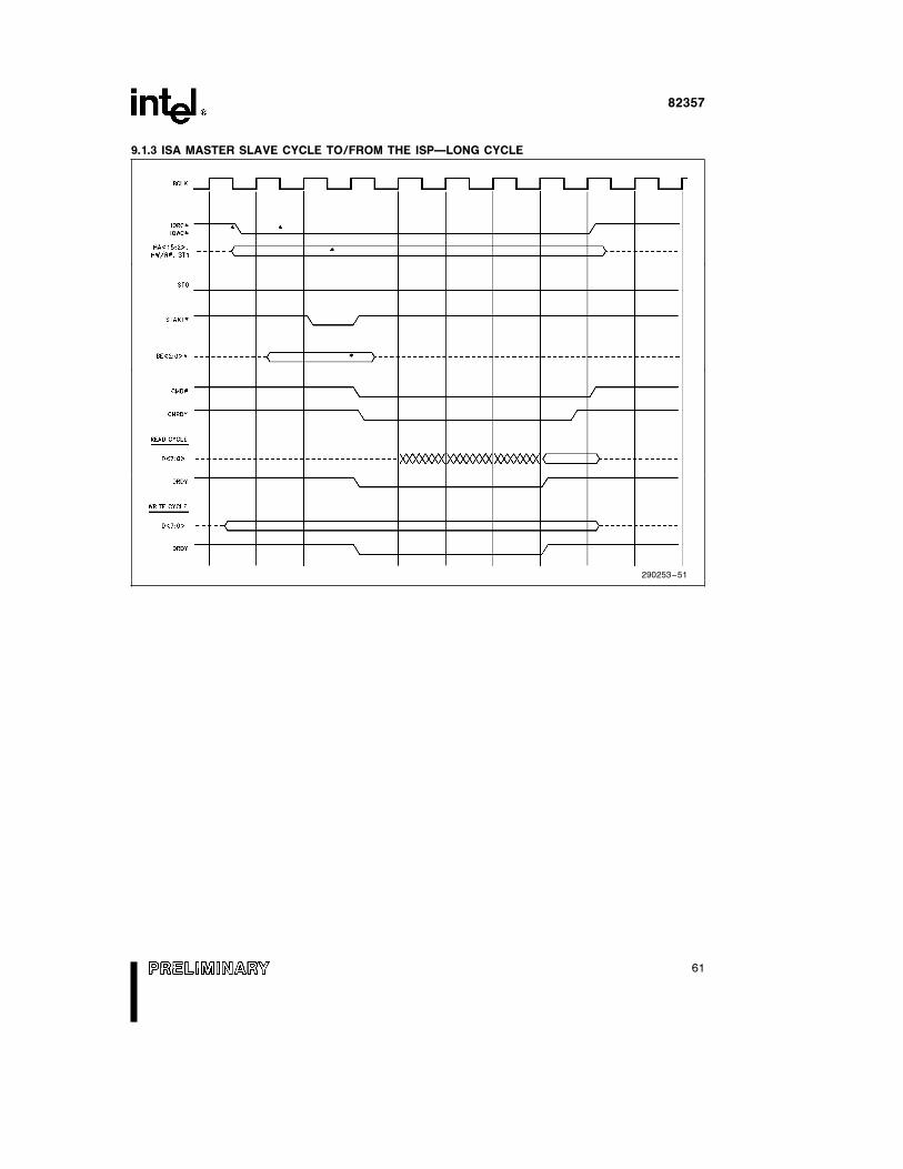
82357
9.1.3 ISA MASTER SLAVE CYCLE TO/FROM THE ISPÐLONG CYCLE
290253–51
61
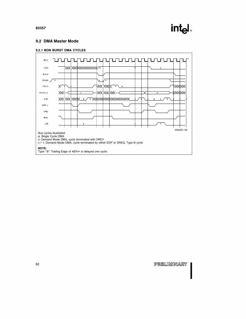
82357
9.2 DMA Master Mode
9.2.1 NON BURST DMA CYCLES
290253–52
Bus cycles illustrated:a: Single Cycle DMAc: Demand Mode DMA, cycle terminated with DRDYca1: Demand Mode DMA, cycle terminated by either EOP or DREQ, Type B cycle
NOTE:Type ‘‘B’’ Trailing Edge of AENÝ is delayed one cycle.
62
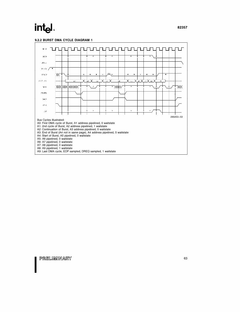
82357
9.2.2 BURST DMA CYCLE DIAGRAM 1
290253–53
Bus Cycles illustrated:A0: First DMA cycle of Burst, A1 address pipelined, 0 waitstateA1: 2nd cycle of Burst, A2 address pipelined, 1 waitstateA2: Continuation of Burst, A3 address pipelined, 0 waitstateA3: End of Burst (A4 not in same page), A4 address pipelined, 0 waitstateA4: Start of Burst, A5 pipelined, 0 waitstateA5: A6 pipelined, 0 waitstateA6: A7 pipelined, 0 waitstateA7: A8 pipelined, 0 waitstateA8: A9 pipelined, 1 waitstateA9: Last DMA cycle, EOP sampled, DREQ sampled, 1 waitstate
63
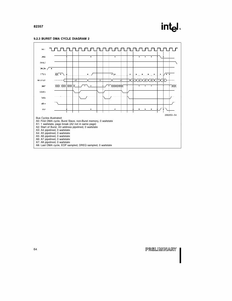
82357
9.2.3 BURST DMA CYCLE DIAGRAM 2
290253–54
Bus Cycles illustrated:A0: First DMA cycle, Burst Slave, non-Burst memory, 0 waitstateA1: 1 waitstate, page break (A2 not in same page)A2: Start of Burst, A3 address pipelined, 0 waitstateA3: A4 pipelined, 0 waitstateA4: A5 pipelined, 0 waitstateA5: A6 pipelined, 0 waitstateA6: A7 pipelined, 0 waitstateA7: A8 pipelined, 0 waitstateA8: Last DMA cycle, EOP sampled, DREQ sampled, 0 waitstate
64
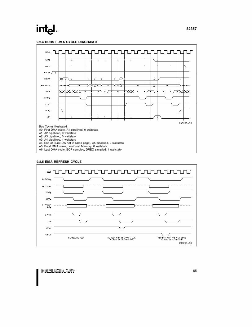
82357
9.2.4 BURST DMA CYCLE DIAGRAM 3
290253–55
Bus Cycles illustrated:A0: First DMA cycle, A1 pipelined, 0 waitstateA1: A2 pipelined, 0 waitstateA2: A3 pipelined, 0 waitstateA3: A4 pipelined, 1 waitstateA4: End of Burst (A5 not in same page), A5 pipelined, 0 waitstateA5: Burst DMA slave, non-Burst Memory, 0 waitstateA6: Last DMA cycle, EOP sampled, DREQ sampled, 1 waitstate
9.2.5 EISA REFRESH CYCLE
290253–56
65
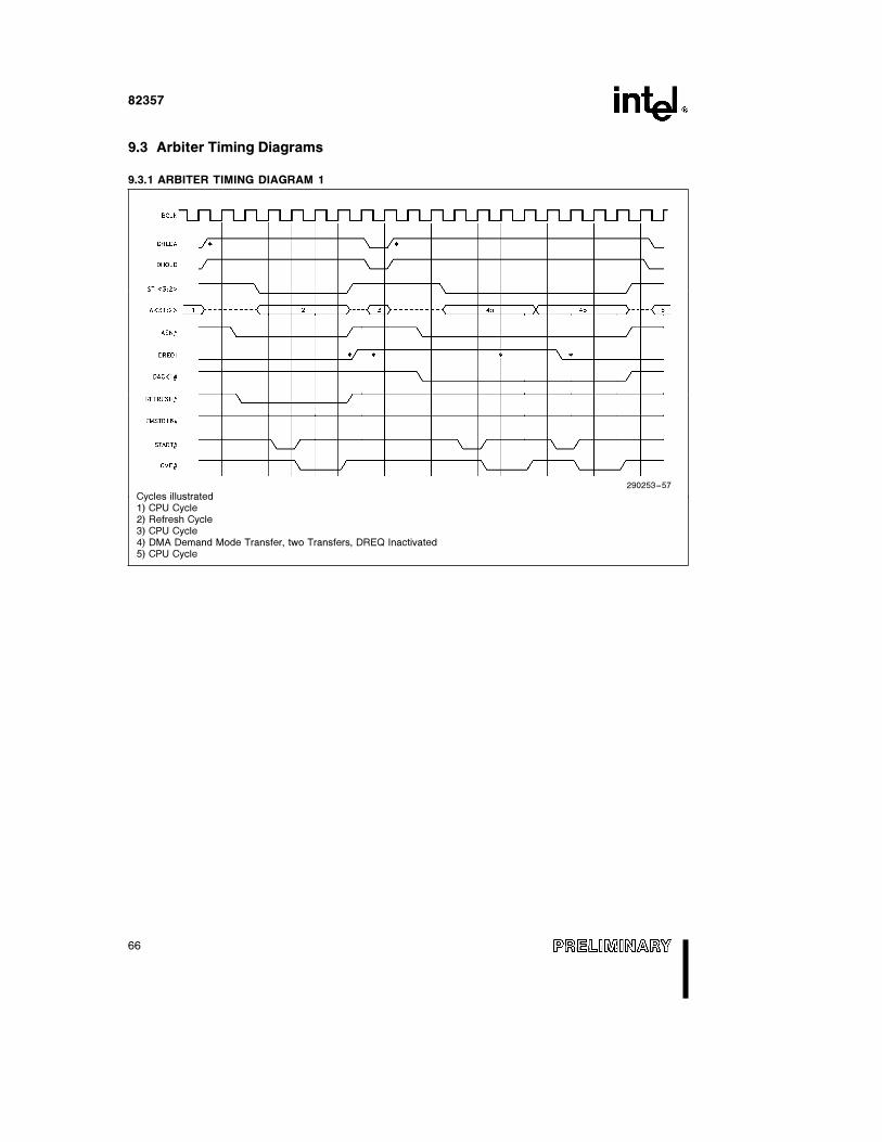
82357
9.3 Arbiter Timing Diagrams
9.3.1 ARBITER TIMING DIAGRAM 1
290253–57
Cycles illustrated1) CPU Cycle2) Refresh Cycle3) CPU Cycle4) DMA Demand Mode Transfer, two Transfers, DREQ Inactivated5) CPU Cycle
66
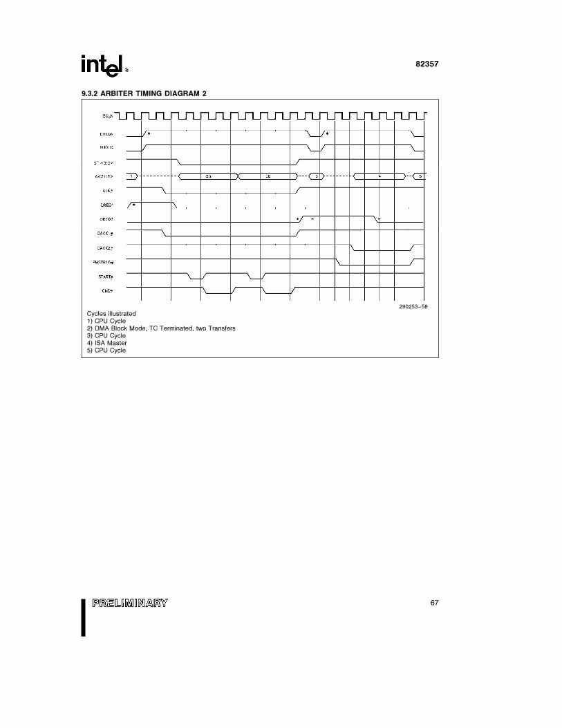
82357
9.3.2 ARBITER TIMING DIAGRAM 2
290253–58
Cycles illustrated1) CPU Cycle2) DMA Block Mode, TC Terminated, two Transfers3) CPU Cycle4) ISA Master5) CPU Cycle
67
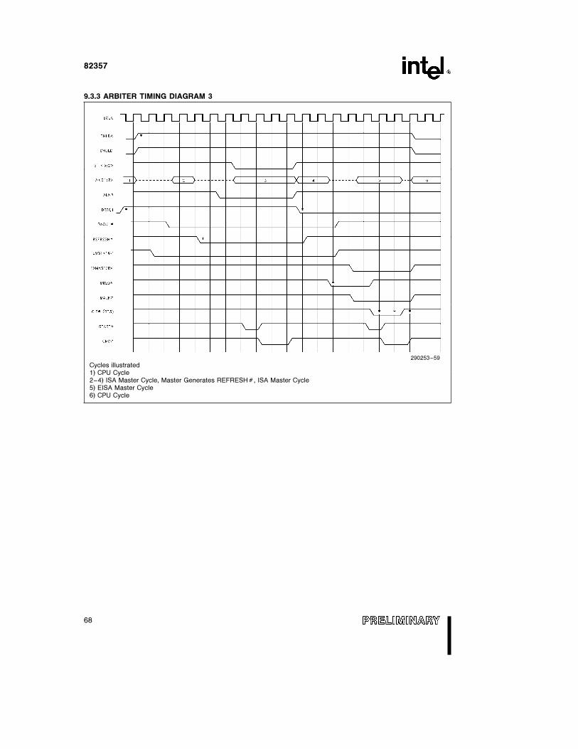
82357
9.3.3 ARBITER TIMING DIAGRAM 3
290253–59
Cycles illustrated1) CPU Cycle2–4) ISA Master Cycle, Master Generates REFRESHÝ, ISA Master Cycle5) EISA Master Cycle6) CPU Cycle
68
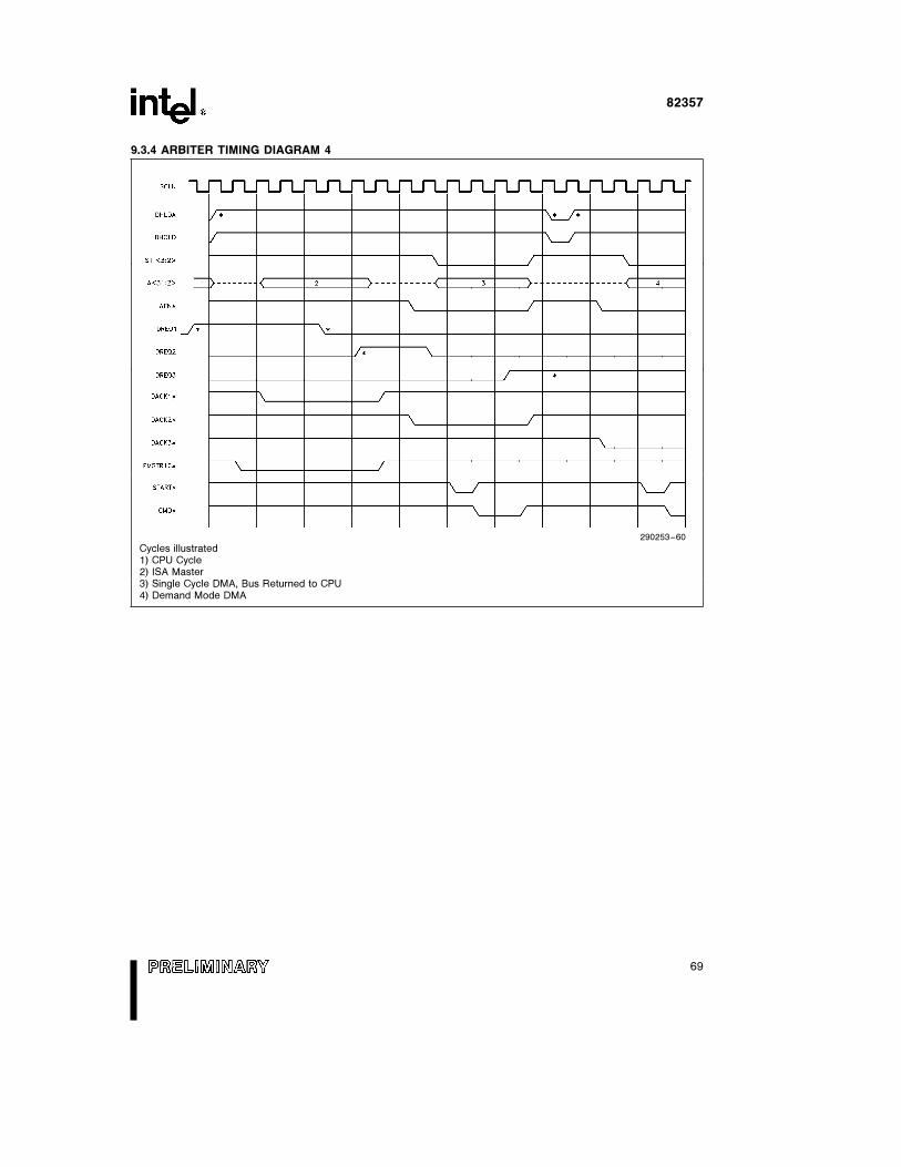
82357
9.3.4 ARBITER TIMING DIAGRAM 4
290253–60
Cycles illustrated1) CPU Cycle2) ISA Master3) Single Cycle DMA, Bus Returned to CPU4) Demand Mode DMA
69
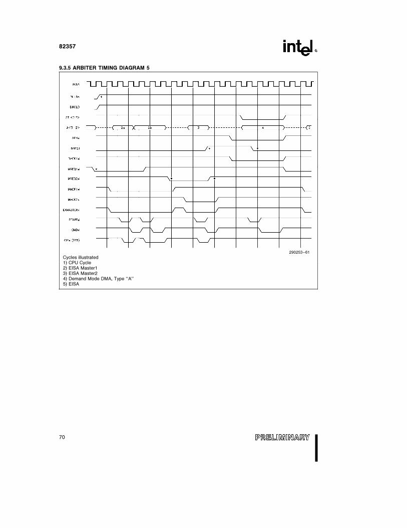
82357
9.3.5 ARBITER TIMING DIAGRAM 5
290253–61
Cycles illustrated1) CPU Cycle2) EISA Master13) EISA Master24) Demand Mode DMA, Type ‘‘A’’5) EISA
70

82357
9.3.6 ARBITER TIMING DIAGRAM 6ÐCIPÝ (ST3Ý) TIMING
290253–62
Cycles illustrated1) Matched EISA Bus Cycle2) Mismatched EISA Bus Cycle, EISA Master Drops MREQ, Bus Controller Drops CIPÝ during Redrive
71
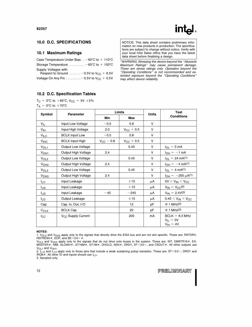
82357
10.0 D.C. SPECIFICATIONS
10.1 Maximum Ratings
Case Temperature Under Bias ÀÀb65§C to a 110§CStorage Temperature ÀÀÀÀÀÀÀÀÀÀb65§C to a 150§CSupply Voltages with
Respect to Ground ÀÀÀÀÀÀÀb0.5V to VCC a 6.5V
Voltage On Any Pin ÀÀÀÀÀÀÀÀÀb0.5V to VCC a 0.5V
NOTICE: This data sheet contains preliminary infor-mation on new products in production. The specifica-tions are subject to change without notice. Verify withyour local Intel Sales office that you have the latestdata sheet before finalizing a design.
*WARNING: Stressing the device beyond the ‘‘AbsoluteMaximum Ratings’’ may cause permanent damage.These are stress ratings only. Operation beyond the‘‘Operating Conditions’’ is not recommended and ex-tended exposure beyond the ‘‘Operating Conditions’’may affect device reliability.
10.2 D.C. Specification Tables
TC e 0§C to a85§C, VCC e 5V g5%
TA e 0§C to a70§C
Symbol ParameterLimits
UnitsTest
Min MaxConditions
VIL Input Low Voltage b0.5 0.8 V
VIH Input High Voltage 2.0 VCC a 0.5 V
VILC BCLK Input Low b0.5 0.8 V
VIHC BCLK Input High VCC b 0.8 VCC a 0.5 V
VOL1 Output Low Voltage 0.45 V IOL e 5 mA
VOH1 Output High Voltage 2.4 V IOH e b1 mA
VOL2 Output Low Voltage 0.45 V IOL e 24 mA(1)
VOH2 Output High Voltage 2.4 V IOH e b4 mA(1)
VOL3 Output Low Voltage 0.45 V IOL e 4 mA(1)
VOH3 Output High Voltage 2.4 V IOH e b250 mA(1)
ILI1 Input Leakage g15 mA 0V k VIN k VCC
ILI2 Input Leakage a15 mA VIN e VCC(2)
ILI3 Input Leakage b45 b240 mA VIN e 2.4V(2)
ILO Output Leakage g15 mA 0.45 k VIN k VCC
Cap Cap. In, Out, I/O 12 pF @ 1 MHz(3)
CCLK BCLK Cap. 20 pF @ 1 MHz(3)
ICC VCC Supply Current 200 mA BCLK e 8.3 MHz
VIL e 0V
VIH e 4V
NOTES:1. VOL2 and VOH2 apply only to the signals that directly drive the EISA bus and are not slot specific. These are: RSTDRV,REFRESHÝ, EOP, and BEk3:0lÝ.VOL3 and VOH3 apply only to the signals that do not drive onto buses in the system. These are: INT, EMSTR16Ý, EX-MASTERÝ, NMI, SLOWHÝ, GT16MÝ, GT1MÝ, DHOLD, AENÝ, DRDY, STk3:0l, and CSOUTÝ. All other outputs useVOL1 and VOH1.2. IL12 and IL13 apply only to those pins that include a weak sustaining pullup transistor. These are: STk3:0l, DRDY andIRQ8Ý. All other IO and inputs should use ILI1.3. Sampled only.
72
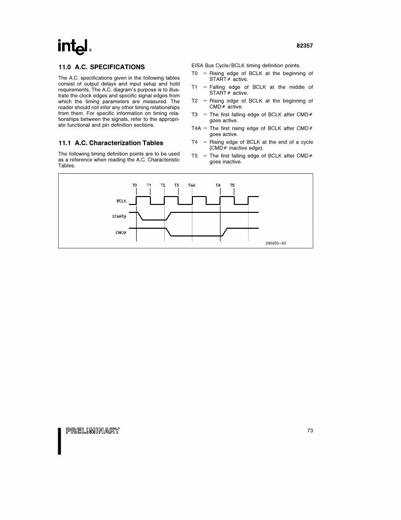
82357
11.0 A.C. SPECIFICATIONS
The A.C. specifications given in the following tablesconsist of output delays and input setup and holdrequirements. The A.C. diagram’s purpose is to illus-trate the clock edges and specific signal edges fromwhich the timing parameters are measured. Thereader should not infer any other timing relationshipsfrom them. For specific information on timing rela-tionships between the signals, refer to the appropri-ate functional and pin definition sections.
11.1 A.C. Characterization Tables
The following timing definition points are to be usedas a reference when reading the A.C. CharacteristicTables.
EISA Bus Cycle/BCLK timing definition points.
T0 e Rising edge of BCLK at the beginning ofSTARTÝ active.
T1 e Falling edge of BCLK at the middle ofSTARTÝ active.
T2 e Rising edge of BCLK at the beginning ofCMDÝ active.
T3 e The first falling edge of BCLK after CMDÝgoes active.
T4A e The first rising edge of BCLK after CMDÝgoes active.
T4 e Rising edge of BCLK at the end of a cycle(CMDÝ inactive edge).
T5 e The first falling edge of BCLK after CMDÝgoes inactive.
290253–63
73
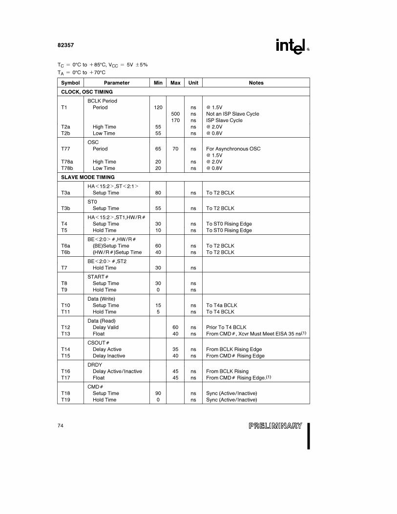
82357
TC e 0§C to a85§C, VCC e 5V g5%
TA e 0§C to a70§C
Symbol Parameter Min Max Unit Notes
CLOCK, OSC TIMING
BCLK Period
T1 Period 120 ns @ 1.5V
500 ns Not an ISP Slave Cycle
170 ns ISP Slave Cycle
T2a High Time 55 ns @ 2.0V
T2b Low Time 55 ns @ 0.8V
OSC
T77 Period 65 70 ns For Asynchronous OSC@ 1.5V
T78a High Time 20 ns @ 2.0V
T78b Low Time 20 ns @ 0.8V
SLAVE MODE TIMING
HAk15:2l,STk2:1l
T3a Setup Time 80 ns To T2 BCLK
ST0
T3b Setup Time 55 ns To T2 BCLK
HAk15:2l,ST1,HW/RÝT4 Setup Time 30 ns To ST0 Rising Edge
T5 Hold Time 10 ns To ST0 Rising Edge
BEk2:0lÝ,HW/RÝT6a (BE)Setup Time 60 ns To T2 BCLK
T6b (HW/RÝ)Setup Time 40 ns To T2 BCLK
BEk2:0lÝ,ST2
T7 Hold Time 30 ns
STARTÝT8 Setup Time 30 ns
T9 Hold Time 0 ns
Data (Write)
T10 Setup Time 15 ns To T4a BCLK
T11 Hold Time 5 ns To T4 BCLK
Data (Read)
T12 Delay Valid 60 ns Prior To T4 BCLK
T13 Float 40 ns From CMDÝ, Xcvr Must Meet EISA 35 ns(1)
CSOUTÝT14 Delay Active 35 ns From BCLK Rising Edge
T15 Delay Inactive 40 ns From CMDÝ Rising Edge
DRDY
T16 Delay Active/Inactive 45 ns From BCLK Rising
T17 Float 45 ns From CMDÝ Rising Edge.(1)
CMDÝT18 Setup Time 90 ns Sync (Active/Inactive)
T19 Hold Time 0 ns Sync (Active/Inactive)
74

82357
Symbol Parameter Min Max Unit Notes
DMA MASTER TIMING
HAk31:2l,HW/RÝ,GT16MÝT22a Delay Valid 1 35 ns Initial Address, HW/RÝ, GT16ÝT22b Delay Valid 1 30 ns Subsequent AddressesT23 Float 1 30 ns (1)
STk3:0l
T24 Delay Active/Inactive 4 37 nsT25 Float 1 40 ns (1)
STk3:2l
T26 Delay Inactive 4 37 ns Burst Cycle/Page Break
DRDYT27 Setup Time 20 nsT28 Hold Time 15 ns
AENÝT29 Delay Active/Inactive 40 ns
BEk3:0lÝT30 Delay Valid 2 45 ns Direct to EISA to Meet Burst TimingsT31 Float 45 ns Float from T3 BCLK.(1)
EOPT32 Delay Active 40 ns Non-BurstT33 Delay Active/Inactive 40 nsT34 Float from DACK 30 ns From DACK Active.(1)
T35 Setup Time 15 ns Sync (Burst Mode)T36 Hold Time 15 ns Sync (Burst Mode)T37 Setup Time 15 ns Async (Non-Burst)T38 Hold Time 15 ns Async (Non-Burst)
ARBITER TIMING
DREQT39 Setup Time 15 ns Sync (Trailing Edge)T40 Hold Time 15 ns Sync (Trailing Edge)T41 Setup Time 15 ns Async (Leading/Trailing Edge)T42 Hold Time 15 ns Async (Leading/Trailing Edge)
MREQÝT43a Setup Time 17 ns BCLK RisingT43b Setup Time 80 ns BCLK Falling, 0.5 BCLKs after T43aT44 Hold Time 15 ns
CPUMISSÝ AsynchronousT45 Setup Time 15 nsT46 Hold Time 15 ns
DHLDA AsynchronousT47 Setup Time 15 nsT48 Hold Time 15 ns
DACKÝT49a Delay Active/Inactive 50 ns 240 pF (ISA Masters)T49b Delay Active/Inactive 50 ns 240 pF (DMA Devices)
MACKÝT50 Delay Active/Inactive 40 ns
DHOLDT51 Delay Active/Inactive 40 ns
75

82357
Symbol Parameter Min Max Unit Notes
ARBITER TIMING (Continued)
EMSTR16ÝT52 Delay Active/Inactive 40 ns
EXMASTERÝT53 Delay Active/Inactive 40 ns
ST3 (CIPÝ)T54 Setup Time 25 nsT55 Hold Time 15 ns
REFRESH TIMING
REFRESHÝT56 Delay Active 55 nsT57 Float Inactive 55 ns
REFRESHÝ AsynchronousT58 Setup Time 15 nsT59 Hold Time 15 ns
RESET TIMING
RST AsynchronousT60 Active Pulse Width 1000 ns 8 BCLKs
RSTDRVT61 Delay Active 60 ns Bus TimeoutT62 Delay Active 60 ns Port/RSTT63 Delay Inactive 60 ns
NMI TIMING
NMIT64 Delay Active/Inactive 60 ns From BCLK Falling EdgeT65 Delay Act 200 ns From OSC Rising Edge
PARITYÝ, IOCHKÝ AsynchronousT66 Setup Time 15 nsT67 Hold Time 15 ns
INTERRUPT TIMING
INTT68 Delay Active/Inactive 500 ns From IRQ Active/InactiveT69 Delay Active/Inactive 500 ns From OSC Rising EdgeT70 Delay Active/Inactive 500 ns From BCLK Falling Edge
COUNTER/TIMER TIMING
SPKRT71 Delay Active/Inactive 200 ns From OSC Rising EdgeT72 Delay Active/Inactive 100 ns From BCLK Falling Edge
SLOWHÝT73 Delay Active/Inactive 200 ns
RTCALE, GTIMÝ TIMING
RTCALET74 Delay Active 55 nsT75 Delay Inactive 40 ns
GT1MÝT76 Delay Active/Inactive 50 ns
NOTE:1. Sampled, not 100% tested.
76
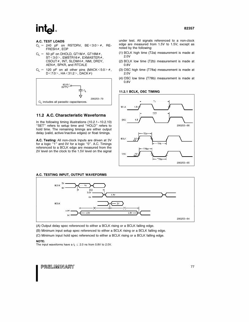
82357
A.C. TEST LOADS
CL e 240 pF on RSTDRV, BEk3:0lÝ, RE-FRESHÝ, EOP
CL e 50 pF on DHOLD, GT1MÝ, GT16MÝ,STk3:0l, EMSTR16Ý, EXMASTERÝ,CSOUTÝ, INT, SLOWHÝ, NMI, DRDY,AENÝ, SPKR, and RTCALE
CL e 120 pF on all other pins (MACKk5:0lÝ,Dk7:0l, HAk31:2l, DACKÝ)
290253–79
CL includes all parasitic capacitances.
11.2 A.C. Characteristic Waveforms
In the following timing illustrations (10.2.1–10.2.10)‘‘SET’’ refers to setup time and ‘‘HOLD’’ refers tohold time. The remaining timings are either outputdelay (valid, active/inactive edges) or float timings.
A.C. Testing: All non-clock Inputs are driven at 3Vfor a logic ‘‘1’’ and 0V for a logic ‘‘0’’. A.C. Timingsreferenced to a BCLK edge are measured from the2V level on the clock to the 1.5V level on the signal
under test. All signals referenced to a non-clockedge are measured from 1.5V to 1.5V; except asnoted by the following:
(1) BCLK high time (T2a) measurement is made at2.0V
(2) BCLK low time (T2b) measurement is made at0.8V
(3) OSC high time (T78a) measurement is made at2.0V
(4) OSC low time (T78b) measurement is made at0.8V
11.2.1 BCLK, OSC TIMING
290253–66
290253–65
A.C. TESTING INPUT, OUTPUT WAVEFORMS
290253–64
(A) Output delay spec referenced to either a BCLK rising or a BCLK falling edge.
(B) Minimum input setup spec referenced to either a BCLK rising or a BCLK falling edge.
(C) Minimum input hold spec referenced to either a BCLK rising or a BCLK falling edge.
NOTE:The input waveforms have a tr s 2.0 ns from 0.8V to 2.0V.
77
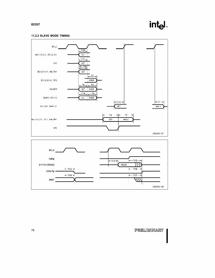
82357
11.2.2 SLAVE MODE TIMING
290253–67
290253–68
78
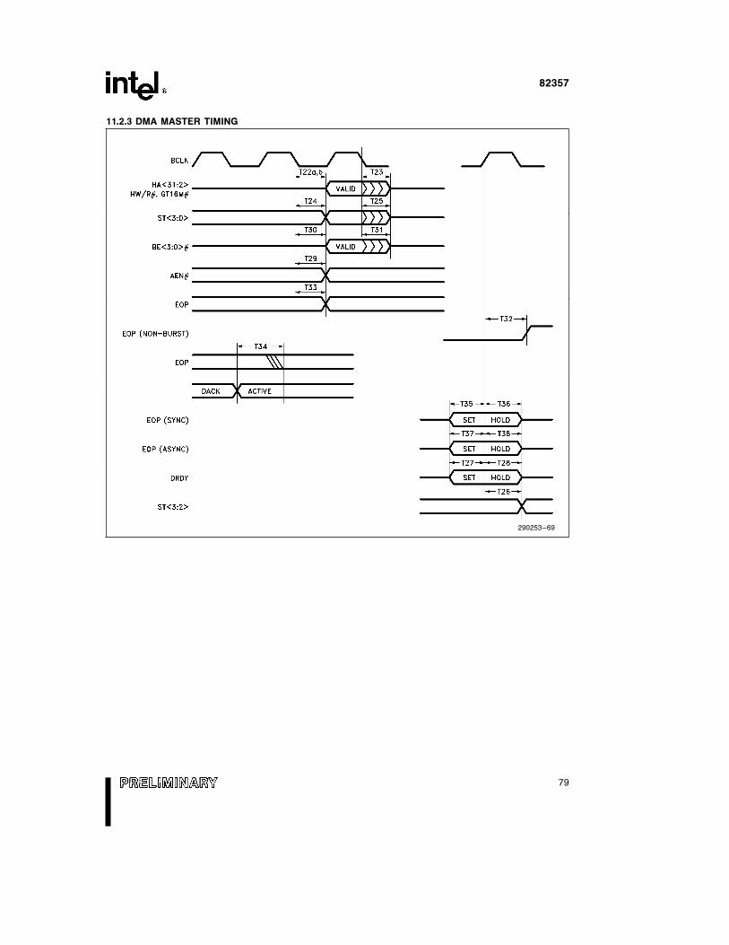
82357
11.2.3 DMA MASTER TIMING
290253–69
79
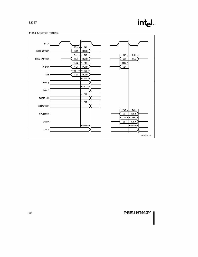
82357
11.2.4 ARBITER TIMING
290253–70
80
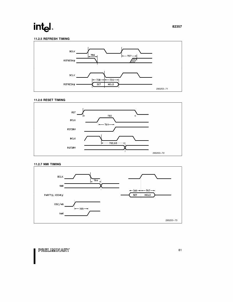
82357
11.2.5 REFRESH TIMING
290253–71
11.2.6 RESET TIMING
290253–72
11.2.7 NMI TIMING
290253–73
81
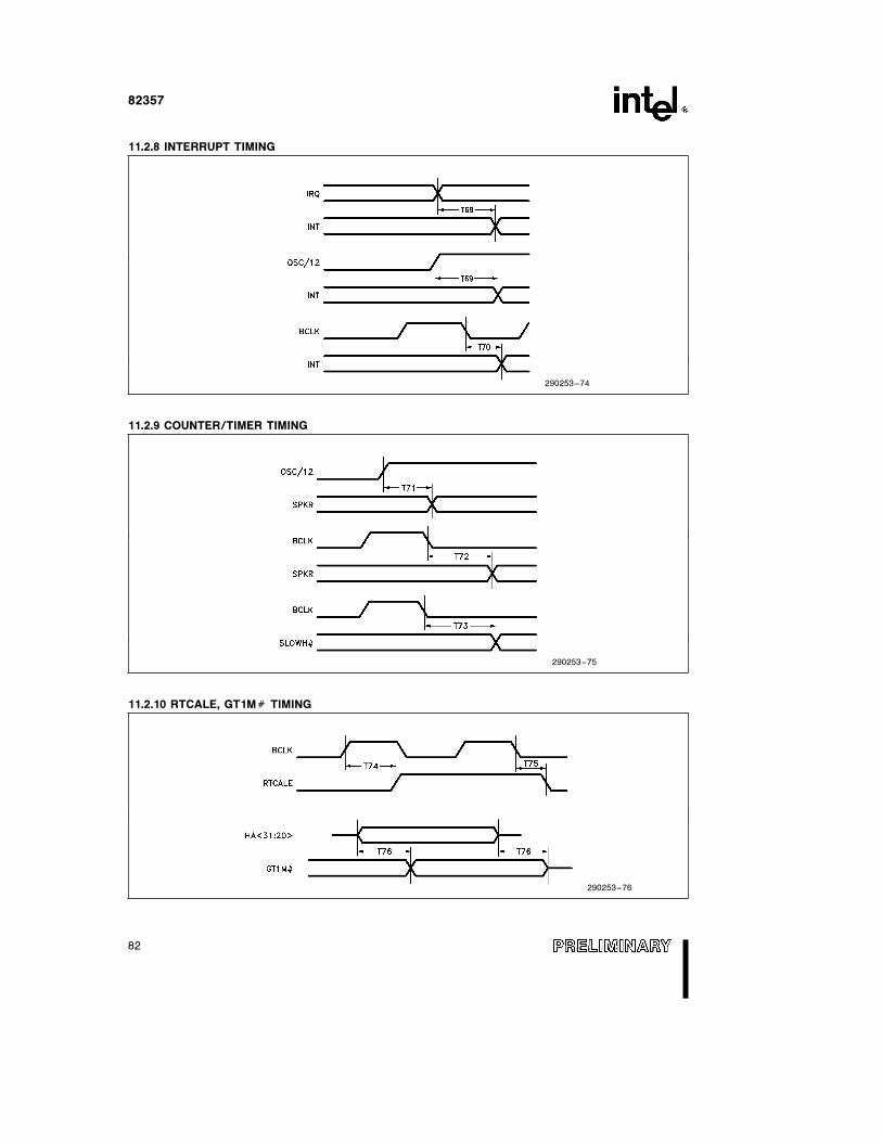
82357
11.2.8 INTERRUPT TIMING
290253–74
11.2.9 COUNTER/TIMER TIMING
290253–75
11.2.10 RTCALE, GT1MÝ TIMING
290253–76
82
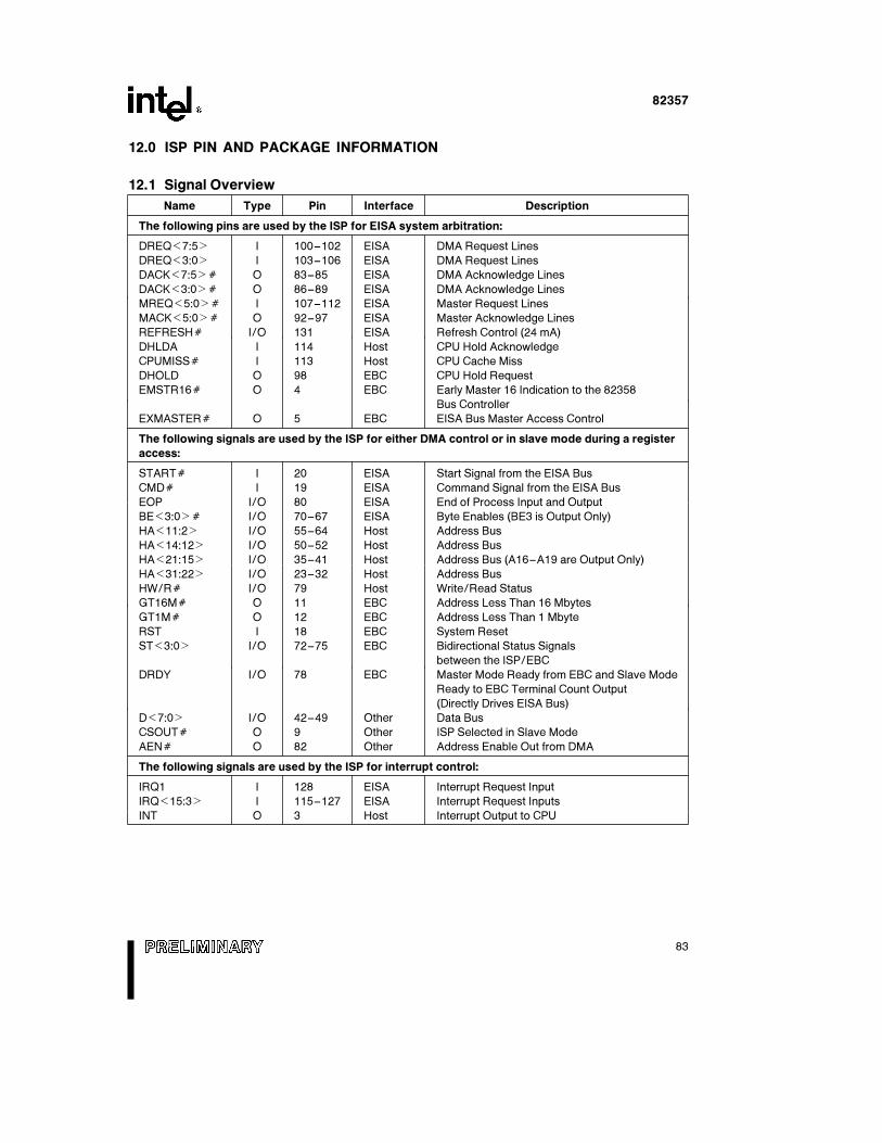
82357
12.0 ISP PIN AND PACKAGE INFORMATION
12.1 Signal Overview
Name Type Pin Interface Description
The following pins are used by the ISP for EISA system arbitration:
DREQk7:5l I 100–102 EISA DMA Request Lines
DREQk3:0l I 103–106 EISA DMA Request Lines
DACKk7:5lÝ O 83–85 EISA DMA Acknowledge Lines
DACKk3:0lÝ O 86–89 EISA DMA Acknowledge Lines
MREQk5:0lÝ I 107–112 EISA Master Request Lines
MACKk5:0lÝ O 92–97 EISA Master Acknowledge Lines
REFRESHÝ I/O 131 EISA Refresh Control (24 mA)
DHLDA I 114 Host CPU Hold Acknowledge
CPUMISSÝ I 113 Host CPU Cache Miss
DHOLD O 98 EBC CPU Hold Request
EMSTR16Ý O 4 EBC Early Master 16 Indication to the 82358
Bus Controller
EXMASTERÝ O 5 EBC EISA Bus Master Access Control
The following signals are used by the ISP for either DMA control or in slave mode during a register
access:
STARTÝ I 20 EISA Start Signal from the EISA Bus
CMDÝ I 19 EISA Command Signal from the EISA Bus
EOP I/O 80 EISA End of Process Input and Output
BEk3:0lÝ I/O 70–67 EISA Byte Enables (BE3 is Output Only)
HAk11:2l I/O 55–64 Host Address Bus
HAk14:12l I/O 50–52 Host Address Bus
HAk21:15l I/O 35–41 Host Address Bus (A16–A19 are Output Only)
HAk31:22l I/O 23–32 Host Address Bus
HW/RÝ I/O 79 Host Write/Read Status
GT16MÝ O 11 EBC Address Less Than 16 Mbytes
GT1MÝ O 12 EBC Address Less Than 1 Mbyte
RST I 18 EBC System Reset
STk3:0l I/O 72–75 EBC Bidirectional Status Signals
between the ISP/EBC
DRDY I/O 78 EBC Master Mode Ready from EBC and Slave Mode
Ready to EBC Terminal Count Output
(Directly Drives EISA Bus)
Dk7:0l I/O 42–49 Other Data Bus
CSOUTÝ O 9 Other ISP Selected in Slave Mode
AENÝ O 82 Other Address Enable Out from DMA
The following signals are used by the ISP for interrupt control:
IRQ1 I 128 EISA Interrupt Request Input
IRQk15:3l I 115–127 EISA Interrupt Request Inputs
INT O 3 Host Interrupt Output to CPU
83
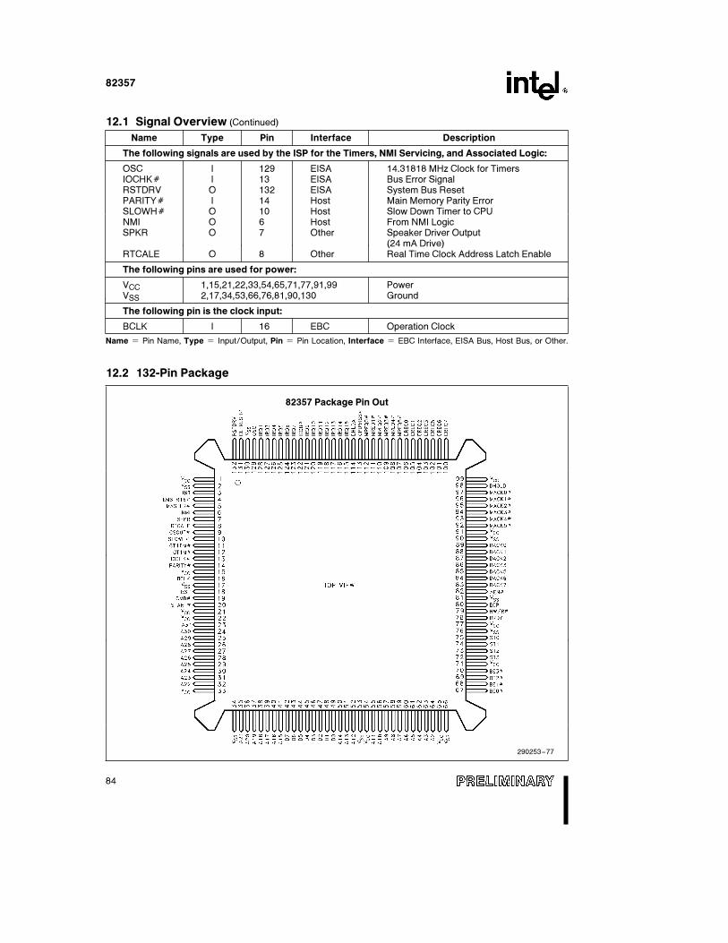
82357
12.1 Signal Overview (Continued)
Name Type Pin Interface Description
The following signals are used by the ISP for the Timers, NMI Servicing, and Associated Logic:
OSC I 129 EISA 14.31818 MHz Clock for TimersIOCHKÝ I 13 EISA Bus Error SignalRSTDRV O 132 EISA System Bus ResetPARITYÝ I 14 Host Main Memory Parity ErrorSLOWHÝ O 10 Host Slow Down Timer to CPUNMI O 6 Host From NMI LogicSPKR O 7 Other Speaker Driver Output
(24 mA Drive)RTCALE O 8 Other Real Time Clock Address Latch Enable
The following pins are used for power:
VCC 1,15,21,22,33,54,65,71,77,91,99 PowerVSS 2,17,34,53,66,76,81,90,130 Ground
The following pin is the clock input:
BCLK I 16 EBC Operation Clock
Name e Pin Name, Type e Input/Output, Pin e Pin Location, Interface e EBC Interface, EISA Bus, Host Bus, or Other.
12.2 132-Pin Package
82357 Package Pin Out
290253–77
84
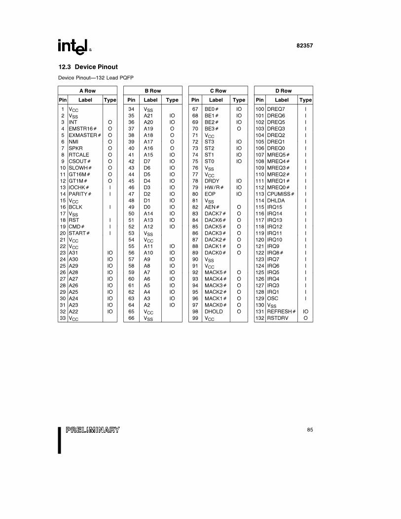
82357
12.3 Device Pinout
Device PinoutÐ132 Lead PQFP
A Row
Pin Label Type
1 VCC
2 VSS
3 INT O
4 EMSTR16Ý O
5 EXMASTERÝ O
6 NMI O
7 SPKR O
8 RTCALE O
9 CSOUTÝ O
10 SLOWHÝ O
11 GT16MÝ O
12 GT1MÝ O
13 IOCHKÝ I
14 PARITYÝ I
15 VCC
16 BCLK I
17 VSS
18 RST I
19 CMDÝ I
20 STARTÝ I
21 VCC
22 VCC
23 A31 IO
24 A30 IO
25 A29 IO
26 A28 IO
27 A27 IO
28 A26 IO
29 A25 IO
30 A24 IO
31 A23 IO
32 A22 IO
33 VCC
B Row
Pin Label Type
34 VSS
35 A21 IO
36 A20 IO
37 A19 O
38 A18 O
39 A17 O
40 A16 O
41 A15 IO
42 D7 IO
43 D6 IO
44 D5 IO
45 D4 IO
46 D3 IO
47 D2 IO
48 D1 IO
49 D0 IO
50 A14 IO
51 A13 IO
52 A12 IO
53 VSS
54 VCC
55 A11 IO
56 A10 IO
57 A9 IO
58 A8 IO
59 A7 IO
60 A6 IO
61 A5 IO
62 A4 IO
63 A3 IO
64 A2 IO
65 VCC
66 VSS
C Row
Pin Label Type
67 BE0Ý IO
68 BE1Ý IO
69 BE2Ý IO
70 BE3Ý O
71 VCC
72 ST3 IO
73 ST2 IO
74 ST1 IO
75 ST0 IO
76 VSS
77 VCC
78 DRDY IO
79 HW/RÝ IO
80 EOP IO
81 VSS
82 AENÝ O
83 DACK7Ý O
84 DACK6Ý O
85 DACK5Ý O
86 DACK3Ý O
87 DACK2Ý O
88 DACK1Ý O
89 DACK0Ý O
90 VSS
91 VCC
92 MACK5Ý O
93 MACK4Ý O
94 MACK3Ý O
95 MACK2Ý O
96 MACK1Ý O
97 MACK0Ý O
98 DHOLD O
99 VCC
D Row
Pin Label Type
100 DREQ7 I
101 DREQ6 I
102 DREQ5 I
103 DREQ3 I
104 DREQ2 I
105 DREQ1 I
106 DREQ0 I
107 MREQ5Ý I
108 MREQ4Ý I
109 MREQ3Ý I
110 MREQ2Ý I
111 MREQ1Ý I
112 MREQ0Ý I
113 CPUMISSÝ I
114 DHLDA I
115 IRQ15 I
116 IRQ14 I
117 IRQ13 I
118 IRQ12 I
119 IRQ11 I
120 IRQ10 I
121 IRQ9 I
122 IRQ8Ý I
123 IRQ7 I
124 IRQ6 I
125 IRQ5 I
126 IRQ4 I
127 IRQ3 I
128 IRQ1 I
129 OSC I
130 VSS
131 REFRESHÝ IO
132 RSTDRV O
85
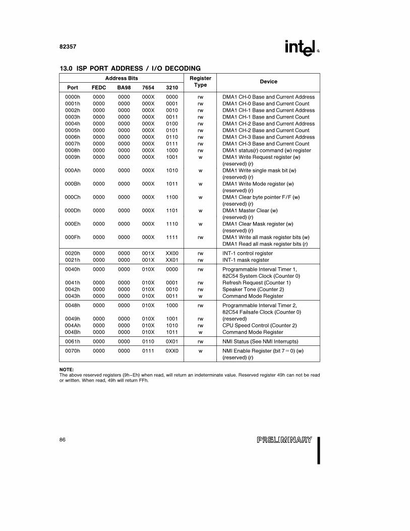
82357
13.0 ISP PORT ADDRESS / I/O DECODING
Address Bits RegisterDevice
Port FEDC BA98 7654 3210Type
0000h 0000 0000 000X 0000 rw DMA1 CH-0 Base and Current Address
0001h 0000 0000 000X 0001 rw DMA1 CH-0 Base and Current Count
0002h 0000 0000 000X 0010 rw DMA1 CH-1 Base and Current Address
0003h 0000 0000 000X 0011 rw DMA1 CH-1 Base and Current Count
0004h 0000 0000 000X 0100 rw DMA1 CH-2 Base and Current Address
0005h 0000 0000 000X 0101 rw DMA1 CH-2 Base and Current Count
0006h 0000 0000 000X 0110 rw DMA1 CH-3 Base and Current Address
0007h 0000 0000 000X 0111 rw DMA1 CH-3 Base and Current Count
0008h 0000 0000 000X 1000 rw DMA1 status(r) command (w) register
0009h 0000 0000 000X 1001 w DMA1 Write Request register (w)
(reserved) (r)
000Ah 0000 0000 000X 1010 w DMA1 Write single mask bit (w)
(reserved) (r)
000Bh 0000 0000 000X 1011 w DMA1 Write Mode register (w)
(reserved) (r)
000Ch 0000 0000 000X 1100 w DMA1 Clear byte pointer F/F (w)
(reserved) (r)
000Dh 0000 0000 000X 1101 w DMA1 Master Clear (w)
(reserved) (r)
000Eh 0000 0000 000X 1110 w DMA1 Clear Mask register (w)
(reserved) (r)
000Fh 0000 0000 000X 1111 rw DMA1 Write all mask register bits (w)
DMA1 Read all mask register bits (r)
0020h 0000 0000 001X XX00 rw INT-1 control register
0021h 0000 0000 001X XX01 rw INT-1 mask register
0040h 0000 0000 010X 0000 rw Programmable Interval Timer 1,
82C54 System Clock (Counter 0)
0041h 0000 0000 010X 0001 rw Refresh Request (Counter 1)
0042h 0000 0000 010X 0010 rw Speaker Tone (Counter 2)
0043h 0000 0000 010X 0011 w Command Mode Register
0048h 0000 0000 010X 1000 rw Programmable Interval Timer 2,
82C54 Failsafe Clock (Counter 0)
0049h 0000 0000 010X 1001 rw (reserved)
004Ah 0000 0000 010X 1010 rw CPU Speed Control (Counter 2)
004Bh 0000 0000 010X 1011 w Command Mode Register
0061h 0000 0000 0110 0X01 rw NMI Status (See NMI Interrupts)
0070h 0000 0000 0111 0XX0 w NMI Enable Register (bit 7e0) (w)
(reserved) (r)
NOTE:The above reserved registers (9h–Eh) when read, will return an indeterminate value. Reserved register 49h can not be reador written. When read, 49h will return FFh.
86
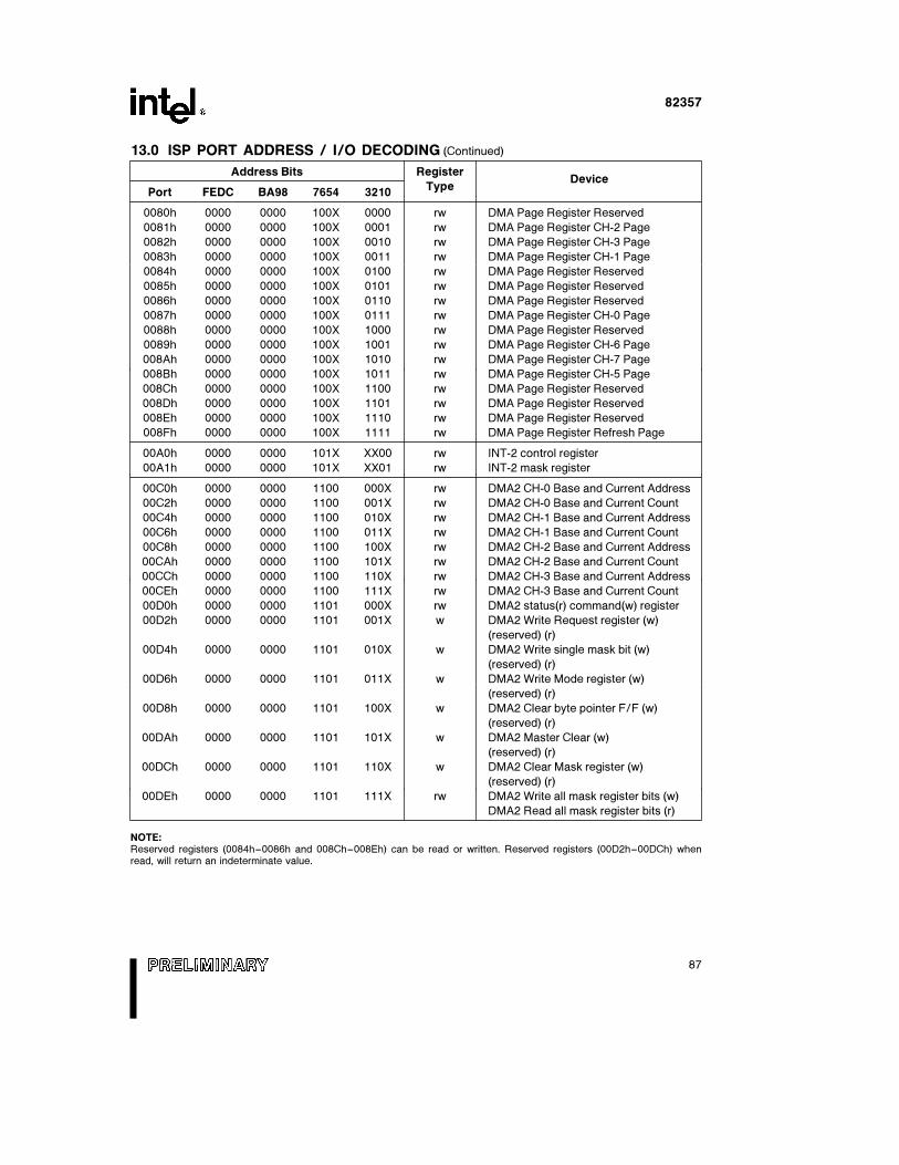
82357
13.0 ISP PORT ADDRESS / I/O DECODING (Continued)
Address Bits RegisterDevice
Port FEDC BA98 7654 3210Type
0080h 0000 0000 100X 0000 rw DMA Page Register Reserved
0081h 0000 0000 100X 0001 rw DMA Page Register CH-2 Page
0082h 0000 0000 100X 0010 rw DMA Page Register CH-3 Page
0083h 0000 0000 100X 0011 rw DMA Page Register CH-1 Page
0084h 0000 0000 100X 0100 rw DMA Page Register Reserved
0085h 0000 0000 100X 0101 rw DMA Page Register Reserved
0086h 0000 0000 100X 0110 rw DMA Page Register Reserved
0087h 0000 0000 100X 0111 rw DMA Page Register CH-0 Page
0088h 0000 0000 100X 1000 rw DMA Page Register Reserved
0089h 0000 0000 100X 1001 rw DMA Page Register CH-6 Page
008Ah 0000 0000 100X 1010 rw DMA Page Register CH-7 Page
008Bh 0000 0000 100X 1011 rw DMA Page Register CH-5 Page
008Ch 0000 0000 100X 1100 rw DMA Page Register Reserved
008Dh 0000 0000 100X 1101 rw DMA Page Register Reserved
008Eh 0000 0000 100X 1110 rw DMA Page Register Reserved
008Fh 0000 0000 100X 1111 rw DMA Page Register Refresh Page
00A0h 0000 0000 101X XX00 rw INT-2 control register
00A1h 0000 0000 101X XX01 rw INT-2 mask register
00C0h 0000 0000 1100 000X rw DMA2 CH-0 Base and Current Address
00C2h 0000 0000 1100 001X rw DMA2 CH-0 Base and Current Count
00C4h 0000 0000 1100 010X rw DMA2 CH-1 Base and Current Address
00C6h 0000 0000 1100 011X rw DMA2 CH-1 Base and Current Count
00C8h 0000 0000 1100 100X rw DMA2 CH-2 Base and Current Address
00CAh 0000 0000 1100 101X rw DMA2 CH-2 Base and Current Count
00CCh 0000 0000 1100 110X rw DMA2 CH-3 Base and Current Address
00CEh 0000 0000 1100 111X rw DMA2 CH-3 Base and Current Count
00D0h 0000 0000 1101 000X rw DMA2 status(r) command(w) register
00D2h 0000 0000 1101 001X w DMA2 Write Request register (w)
(reserved) (r)
00D4h 0000 0000 1101 010X w DMA2 Write single mask bit (w)
(reserved) (r)
00D6h 0000 0000 1101 011X w DMA2 Write Mode register (w)
(reserved) (r)
00D8h 0000 0000 1101 100X w DMA2 Clear byte pointer F/F (w)
(reserved) (r)
00DAh 0000 0000 1101 101X w DMA2 Master Clear (w)
(reserved) (r)
00DCh 0000 0000 1101 110X w DMA2 Clear Mask register (w)
(reserved) (r)
00DEh 0000 0000 1101 111X rw DMA2 Write all mask register bits (w)
DMA2 Read all mask register bits (r)
NOTE:Reserved registers (0084h–0086h and 008Ch–008Eh) can be read or written. Reserved registers (00D2h–00DCh) whenread, will return an indeterminate value.
87
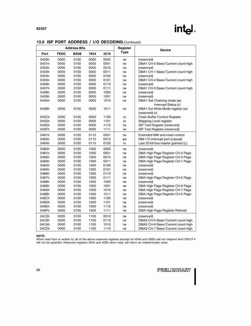
82357
13.0 ISP PORT ADDRESS / I/O DECODING (Continued)
Address Bits RegisterDevice
Port FEDC BA98 7654 3210Type
0400h 0000 0100 0000 0000 rw (reserved)
0401h 0000 0100 0000 0001 rw DMA1 CH-0 Base/Current count high
0402h 0000 0100 0000 0010 rw (reserved)
0403h 0000 0100 0000 0011 rw DMA1 CH-1 Base/Current count high
0404h 0000 0100 0000 0100 rw (reserved)
0405h 0000 0100 0000 0101 rw DMA1 CH-2 Base/Current count high
0406h 0000 0100 0000 0110 rw (reserved)
0407h 0000 0100 0000 0111 rw DMA1 CH-3 Base/Current count high
0408h 0000 0100 0000 1000 rw (reserved)
0409h 0000 0100 0000 1001 rw (reserved)
040Ah 0000 0100 0000 1010 rw DMA1 Set Chaining mode (w)
Interrupt Status (r)
040Bh 0000 0100 0000 1011 rw DMA1 Ext Write Mode register (w)
(reserved) (r)
040Ch 0000 0100 0000 1100 ro Chain Buffer Control Register
040Dh 0000 0100 0000 1101 ro Stepping Level register
040Eh 0000 0100 0000 1110 rw ISP Test Register (reserved)
040Fh 0000 0100 0000 1111 rw ISP Test Register (reserved)
0461h 0000 0100 0110 0001 rw Extended NMI and reset control
0462h 0000 0100 0110 0010 wo NMI I/O interrupt port (casual)
0464h 0000 0100 0110 0100 ro Last 32-bit bus master granted (L)
0480h 0000 0100 1000 0000 rw (reserved)
0481h 0000 0100 1000 0001 rw DMA High Page Register CH-2 Page
0482h 0000 0100 1000 0010 rw DMA High Page Register CH-3 Page
0483h 0000 0100 1000 0011 rw DMA High Page Register CH-1 Page
0484h 0000 0100 1000 0100 rw (reserved)
0485h 0000 0100 1000 0101 rw (reserved)
0486h 0000 0100 1000 0110 rw (reserved)
0487h 0000 0100 1000 0111 rw DMA High Page Register CH-0 Page
0488h 0000 0100 1000 1000 rw (reserved)
0489h 0000 0100 1000 1001 rw DMA High Page Register CH-6 Page
048Ah 0000 0100 1000 1010 rw DMA High Page Register CH-7 Page
048Bh 0000 0100 1000 1011 rw DMA High Page Register CH-5 Page
048Ch 0000 0100 1000 1100 rw (reserved)
048Dh 0000 0100 1000 1101 rw (reserved)
048Eh 0000 0100 1000 1110 rw (reserved)
048Fh 0000 0100 1000 1111 rw DMA High Page Register Refresh
04C2h 0000 0100 1100 0010 rw (reserved)
04C6h 0000 0100 1100 0110 rw DMA2 CH-5 Base/Current count high
04CAh 0000 0100 1100 1010 rw DMA2 CH-6 Base/Current count high
04CEh 0000 0100 1100 1110 rw DMA2 CH-7 Base/Current count high
NOTE:When read from or written to, all of the above reserved registers (except for 40Ah and 40Bh) will not respond and CSOUTÝwill not be asserted. Reserved registers 40Ah and 40Bh when read, will return an indeterminate value.
88
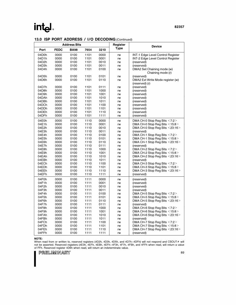
82357
13.0 ISP PORT ADDRESS / I/O DECODING (Continued)
Address Bits RegisterDevice
Port FEDC BA98 7654 3210Type
04D0h 0000 0100 1101 0000 rw INT-1 Edge Level Control Register04D1h 0000 0100 1101 0001 rw INT-2 Edge Level Control Register04D2h 0000 0100 1101 0010 rw (reserved)04D3h 0000 0100 1101 0011 rw (reserved)04D4h 0000 0100 1101 0100 rw DMA2 Set Chaining mode (w)
Chaining mode (r)04D5h 0000 0100 1101 0101 rw (reserved)04D6h 0000 0100 1101 0110 rw DMA2 Ext Write Mode register (w)
(reserved) (r)04D7h 0000 0100 1101 0111 rw (reserved)04D8h 0000 0100 1101 1000 rw (reserved)04D9h 0000 0100 1101 1001 rw (reserved)04DAh 0000 0100 1101 1010 rw (reserved)04DBh 0000 0100 1101 1011 rw (reserved)04DCh 0000 0100 1101 1100 rw (reserved)04DDh 0000 0100 1101 1101 rw (reserved)04DEh 0000 0100 1101 1110 rw (reserved)04DFh 0000 0100 1101 1111 rw (reserved)
04E0h 0000 0100 1110 0000 rw DMA CH-0 Stop Reg Bits k7:2l
04E1h 0000 0100 1110 0001 rw DMA CH-0 Stop Reg Bits k15:8l
04E2h 0000 0100 1110 0010 rw DMA CH-0 Stop Reg Bits k23:16l
04E3h 0000 0100 1110 0011 rw (reserved)04E4h 0000 0100 1110 0100 rw DMA CH-1 Stop Reg Bits k7:2l
04E5h 0000 0100 1110 0101 rw DMA CH-1 Stop Reg Bits k15:8l
04E6h 0000 0100 1110 0110 rw DMA CH-1 Stop Reg Bits k23:16l
04E7h 0000 0100 1110 0111 rw (reserved)04E8h 0000 0100 1110 1000 rw DMA CH-2 Stop Reg Bits k7:2l
04E9h 0000 0100 1110 1001 rw DMA CH-2 Stop Reg Bits k15:8l
04EAh 0000 0100 1110 1010 rw DMA CH-2 Stop Reg Bits k23:16l
04EBh 0000 0100 1110 1011 rw (reserved)04ECh 0000 0100 1110 1100 rw DMA CH-3 Stop Reg Bits k7:2l
04EDh 0000 0100 1110 1101 rw DMA CH-3 Stop Reg Bits k15:8l
04EEh 0000 0100 1110 1110 rw DMA CH-3 Stop Reg Bits k23:16l
04EFh 0000 0100 1110 1111 rw (reserved)
04F0h 0000 0100 1111 0000 rw (reserved)04F1h 0000 0100 1111 0001 rw (reserved)04F2h 0000 0100 1111 0010 rw (reserved)04F3h 0000 0100 1111 0011 rw (reserved)04F4h 0000 0100 1111 0100 rw DMA CH-5 Stop Reg Bits k7:2l
04F5h 0000 0100 1111 0101 rw DMA CH-5 Stop Reg Bits k15:8l
04F6h 0000 0100 1111 0110 rw DMA CH-5 Stop Reg Bits k23:16l
04F7h 0000 0100 1111 0111 rw (reserved)04F8h 0000 0100 1111 1000 rw DMA CH-6 Stop Reg Bits k7:2l
04F9h 0000 0100 1111 1001 rw DMA CH-6 Stop Reg Bits k15:8l
04FAh 0000 0100 1111 1010 rw DMA CH-6 Stop Reg Bits k23:16l
04FBh 0000 0100 1111 1011 rw (reserved)04FCh 0000 0100 1111 1100 rw DMA CH-7 Stop Reg Bits k7:2l
04FDh 0000 0100 1111 1101 rw DMA CH-7 Stop Reg Bits k15:8l
04FEh 0000 0100 1111 1110 rw DMA CH-7 Stop Reg Bits k23:16l
04FFh 0000 0100 1111 1111 rw (reserved)
NOTE:When read from or written to, reserved registers (4D2h, 4D3h, 4D5h, and 4D7h–4DFh) will not respond and CSOUTÝ willnot be asserted. Reserved registers (4E3h, 4EFh, 4EBh, 4EFh–4F3h, 4F7h, 4FBh, and 4FFh when read, will return a valueof FFh. Reserved register 4D6h when read, will return an indeterminate value.
89

82357
14.0 THERMAL SPECIFICATION
The 82357 is specified for operation when the casetemperature is within the range of 0§C–85§C. Thecase temperature may be measured in any environ-ment, to determine whether the device is within thespecified operating range.
The PQFP case temperature should be measured atthe center of the top surface opposite the pins, asshown in Figure 14-1 below.
Process Name: CHMOSIV
Temperature Rise Vs. Time:
Time (sec) Temperature Rise
Unit Power (§C/w)
0 0
1 3.7
2 6.0
3 7.3
5 9.5
290253–80
Figure 14-1. Plastic Quad Flat Pack (PQFP)
Table 14-1. 82357 PQFP Package Thermal Characteristics
Thermal ResistanceЧC/Watt
ParameterAir Flow Rate (Ft/Min)
0 200 400 600 800
i Junction to Case 7 7 7 7 7
i Case to Ambient 22 17.5 14.5 12 10
NOTES:1. Table 14-1 applies to the 82357 PQFP plugged into a socket or soldered directly on to the board.2. iJA e iJC a iCA.
90
82357
15.0 REVISION HISTORY
This data sheet contains updates and improvements between versions -003 and -004. A revision summary islisted here for your convenience.
82357 Integrated System Peripheral (ISP)
Highlights Reference was added to 82350DT.
Section 3.7.1 Text for I/O writes was revised.
Section 11.1 t10 is 15 ns minimum. t30 is 2 ns min. t43a is 16 ns minimum.
Note 1 was deleted from t22b, and added to t23.
Section 12.4 Add thermal specification.
This data sheet contains updates and improvements between versions -004 and -005. A revision summary islisted here for your convenience.
82357 Revision Summary
Section 1.0 In Figure 1-1 ISP System Interface, the REFRESHÝ pin was corrected to indicate I/Ofunction.
Section 2.3 In 2nd paragraph in left-handed column, EXMASTER16Ý was changed to EMSTR16Ý.
Section 7.1.3 In Figure 7-4, Status Byte format, Returned Status bit changed. Bit 6 should be 0eCRcontents are moved into CE. 1eCR contents not moved into CE.
Section 8.1 In CPUMISSÝ pin description, deleted the line, ‘‘This line may be tied active in a cache-less system.’’ Added ‘‘This signal should not be generated to the ISP when the CPU orcache own the bus (i.e., when HLDA is inactive).’’
In EXMASTERÝ signal description, the last sentence changed to read ‘‘This signal isdriven active and inactive with MACKÝ on the rising edge of BCLK, except in the case ofPREEMPT. In this case, EXMASTERÝ is negated on the same rising BCLK edge thatCIPÝ (ST3) is sampled active.’’ The last sentence was not changed.
Section 9.1.2, 9.1.3 Figure 9.1.2 IORDÝ and IOWRÝ were changed to IORCÝ and IOWCÝ, and ST0 waschanged to be LOW (i.e., 0) during entire diagram.
Section 9.3 Corrected CHRDY to deassert after the falling edge during the eighth BCLK.
Section 11.1 T13 had Note 1 added. t43a changed from 16 ns to 17 ns min.
Section 13.0 040CH device description changed to ‘‘chain buffer control register’’ (3) 04E0h shouldreference bits k7:2l NOT k7:3l.
82357 Revision Summary
The following changes have been made since revision 005:
Section 8.1 REFRESHÝ paragraph heading corrected to read ‘‘REFRESHÝ I/O OPEN COLLECTOR
(REFRESH)’’.
Section 10.2 Test Conditions for Symbol VOL3 has been corrected to IOL e 4 mA(1).
Section 14.0 Table 14-1 note 2 has been corrected to read iJA e iJC a iCA.
91