Embed Size (px)
Citation preview

A 1.8V 2nd-Order CA Modulator
by
Wei Yang
A thesis submitted in conformity with the requirements for the degree of Master of Applied Science
Department of Electrical and Cornputer Engineering University of Toronto
1999
O Copyright by Wei Yang 1999
National Library 141 of Canada Bibliothèque nationale du Canada
Acquisitions and Acquisitions et Bibliographie Services services bibliographiques
395 Wellington Street 395, rue Wellington OnawaON K1AON4 Ottawa ON KtA O N 4 Canada Canada
The author has granted a non- exclusive licence allowuig the National Library of Canada to reproduce, loan, distribute or sel1 copies of this thesis in microforni, paper or electronic formats.
The author retains ownership of the copyright in this thesis. Neither the thesis nor substantial extracts f?om it may be printed or otherwise reproduced without the author's permission.
L'auteur a accordé une licence non exclusive permettant à la Bibliothèque nationale du Canada de reproduire, prêter, distribuer ou vendre des copies de cette thèse sous la forme de microfiche/filtn, de reproduction sur papier ou sur format électronique.
L'auteur conserve la propriété du droit d'auteur qui protège cette thèse. Ni la thèse ni des extraits substantiels de celle-ci ne doivent être imprimés ou autrement reproduits sans son autorisation.

A l.SV 2nd-Order CA Modulator
Wei Yang
Master of Applied Science, 1999
Department of Electrical and Computer Engineering
University of Toronto
Abstract
Low-vol tage, low-power analog-to-digi ta1 converters provide a cr i tical interface in
portable mixed-signal electronic systems. The robustness and tolerance of the sigma-delta
modulator technique over other data-converter techniques rnake it an ideal choice in
applications where low voltage and high-dynamic range are a must.
This thesis deals with the design and irnplementation of a low-voltage. low-power 2nd-
order sigma-delta modulator with a single 1.8 V power supply using conventional threshold
voltage transistors. Al1 the circuit blocks are integrated on one chip. and the input common-
mode voltage is set at mid-rail. resulting in low power dissipation, minimum off-chip
components, and high efficiency, Bexibility and conipatibility. The design is useful for voice
applications in personai communications systems supplied by two nickel-cadmium or
alkaline batteries.
The modulator consists of four circuit blocks: the biasing, the operational amplifier, the
comparator-latch, and the four-phase clock generator. A high DC gain, large output swing
operational amplifier with a low-voltage power supply was implemented using a fully-
differential folded-cascode input stage followed by a common-source output stage,
combined w i th a switched-capacitor common-mode feedback circuit. Based on full y-
differential switched-capacitor techniques, the modulator was implemented using a 3.3 V,
double-poly, 0.35pm CMOS process. The rnodulator exhibits a 15-bit dynamic range for a
7 kHz bandwidth, and a 14-bit dynarnic range for a 20 kHz bandwidth at an oversampling
frequency of 2.56 MHz. The complete 2nd-order modulator h a a power dissipation of
0.99 mW, and occupies 0.3 1 mm2 of die area excluding bonding pads.

Acknowledgments
1 would like to express rny sincere gratitude to University Professor C.A.T. Salama for
his guidance and assistance throughout the course of this research work.
1 would like to thank Professor Wai Tung Ng for his great heip at the beginning of this
work.
1 am indebted to Ning Ge. and Derek Hing Sang Tarn, for their invaluable technical
advice and help in designing and implementing the chip.
My sincere thanks to Khoman Phang and Hormoz Djahanshahi for their helpful
assistance and suggestions on the chip implementation. Thanks to Dod Chettiar for his
kindly help and suggestions on the chip testing. Thanks to Jaro Pristupa for his technical
support with the CAD tools. My appreciation extends to al1 the staff and students in the
Microelectronic Research Laboratory, especially to Naoto Fushijima, An Wei. Sotoudeh
Hamedi-Hagh, and Mehrdad Ramezani for al1 their invaluable discussions and instructions.
I am specially grateful to Anthoula Vlahakis for her warm-hearted assistance from the
beginning to the end of the work.
1 would like to thank Lynda Wu for her encouragement, friendship and trust.
A special word of thanks to my friend, Ming Hou, who keeps me Company with a
constant source of support. encouragement. and friendship.
This support of Micronet, Gennum, Mitel, Nonel Networks, and PMC-Sierra is
gratefully ac know ledged.
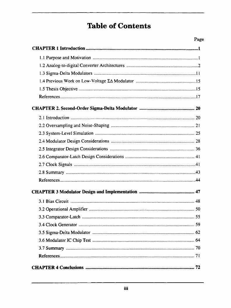
Table of Contents
Page
CHAPTER 1 Introduction ............................................................................................. 1
.......................................................................................... 1.1 Purpose and Motivation 1
7 1.2 Analog-to-digital Converter Architectures .............................................................. ....................................................................................... 1.3 Sigma-Delta Modulators 11
................................................... 1.4 Previous Work on Low-Voltage XA Modulator 15
1.5 Thesis Objective .................................................................................................... 15
References .................................................................................................................... 17
............................................... . CHAPTER 2 Second-Order Sigma-Delta Modulator 20
2.1 introduction .......................................................................................................... 20
2.2 Oversampling and Noise-Shaping .......................... .. .................................... 21
2.3 System-Level Simulation .................................................................................... 25
....................................................................... 2.4 Modulütor Design Considerations 28
............................*......... ............................. 2.5 Integrator Design Considerations ... 36
........................................................... 2.6 Comparator-Latch Design Considerations JI
2.7 Clock Signals ........................................................................................................ 41
2.8 Summary ............................................................................................................... 43
................................................................................................................... References -44
.................... CHAPTER 3 Modulator Design and Implementation .... ............. 47
3.1 Bias Circuit .......................................................................................................... 48
3.2 Operationai Amplifier .......................................................................................... 50
................................................................................................ 3.3 Comparator-Latch 55
................................................................................................... 3.4 Clock Generator 59
3.5 Sigma-Delta Modulator ....................................................................................... 62
3.6 Modulator IC Chip Test ....................................................................................... 64
3.7 Summary .............................................................................................................. 70
References ................................................................................................................... 71
CHAPTER 4 Conclusions .......................................... .... ...............a........... 72
Page
.......................................................................... APPENDIX Modulator IC Chip Test 74
A . 1 Test Topology ..................................................................................................... 74
A.2 Equipment and Setup ........................................................................................... 75
A.3 Test Board ............................................................................................................ 76
A.4 Test procedure ...................................................................................................... 77
List of Figures
Fig . 1.1:
Fig . 1.2:
Fig . 1.3:
Fig . 1.4:
Fig . 1.5:
Fig . 1.6:
Fig . 1.7:
Fig . 1.8:
Fig . 1.9:
Page
......................................................................... Conventional Nyquist-rate ADC 3
.................................................................................. ParaIlel AûC Architecture 3
................................................... Successive-Approximation ADC Architecture 4
........................................................................... Algorithmic ADC Architecture 5
............................................. ......................... Integnting ADC Architecture .. 6
............................................................................ Subranging ADC Architecture 7
............................................................................................. Oversampling ADC 8
.......................................................................... S igma-Delta ADC Architecture 9
................................ ................... Cornparison of ADC's Conversion Speed .. I O
Fig . 1.10. Trading Conversion Speed for Resolution ................................................... I l
............................................... Fig . 1.1 1 : Second-Order Sigma-Delta ADC Architecture 14
............................................... Fig . 2.1 : Second-Order Sigma-Del ta Modulator Diagrarn 20
37 ................................................................................... . Fig 2.2. Modulator Linear Mode1 -- ............................................................ Fig . 2.3 : Second-Order Noise-S haping S truccure 24
....................................................... . Fig 2.4. Sigma-Delta Quantization Noise Spectrum 24
....................... Fig . 2.5. Simulink Set-up Configuration for A 2nd-Order ZA Modulator 26
.................................................................. Fig . 2.6. Full Spectrum of Modulator Output 27
......................................... . Fig 2.7. Plot of S N R versus Norrnalized Signal Input Ievel 27
.......................... Fig . 2.8 : Practical Second-Order Sigma-Del ta Modulator Architecture 28
......................................................................... . Fig 2.9. Noise Power Spectral Densities 32
.................................................... . Fig 2.10. Switched-Capacitor Integrator Architecture 36
.......................... Fig . 2.1 1: Timing Wavefonns of Two-Phase Non-overlapping Clocks 42
..... Fig . 3.1 : Block Diagram of the Second-Order Sigma-Delta Modulator Architecture 47
Fig . 3.2. Bias Circuit Architecture ................................................................................... 48
....................................................................................... Fig . 3.3. Layout of Bias Circuit 50
Fig . 3.4. Differential Stage of Operational Amplifier ...................................................... 51
........................................................................ Fig . 3.5. Comrnon-mode Feedback Stage 52
Fig . 3.6. Layout of Operational Amplifier ....................................................................... 54
............................................ . Fig 3.7. Post-Layout Simulation of Operational Amplifier 55
........................................................... . Fig 3.8. Schematic Design of Comparator-Latch 56
Fig . 3.9. &Phase Clock Signals ....................................................................................... 58
............................................................................... . Fig 3.10. Comparator-Latch Layout 58
............................................. Fig . 3.1 1 : Post-Layout Simulation of Compantor-Latch 59
Fig . 3.12. Schematic of Clock Generator ........................................................................ 60
.................................................................................. Fig . 3.13. Clock Generator Layout 61
....................................................... Fig . 3.14. Clock Generator Post-Layout Simulation 61
.................. Fig . 3.15. Die Micrograph of the 2nd-order LA Modulator Implementation 63
........................................................... Fig . 3 . 16: Measured clk 1 and cIk2 Clock Signals 65
.................................................................. Fig . 3.17. Inverting Amplifier Configuration 65
................................................... Fig . 3 . 18: Gain Performance of Operational Amplifier 66
................................. Fig . 3.19. Measured Pulse-Densi ty-Modulated Modulator Output 67
................ Fig . 3.20. Reconstructed Input Signal from the Measured Modulator Output 67
......................................... Fig . 3.2 1 : Full Spectmm of the Measured Modulator Output 68
........................... Fig . 3.22. Measured SNR and SNDR versus Normalized Input Level 68
Fig . A . 1 : Test Setup for EA Moduiütor [C .................................................................... 75
............................................. Fig . A.2. PCB Test Board for the Sigma-Delta Modulator 76

List of Tables
Page
Table 1 . 1 : Recent Work on Low Voltage ZA Modulator ................................................ 15
..................................................................... Table 3.1 : B i s Circuit Component Values 49
Table 3.2. Post-layout Simulation Results of Bias Circuit .............................................. 50
Table 3.3. Differential Stage Component Values ............................................................ 52
..................................... Table 3.4. Common-mode Feedback Stage Component Values 53
...................................... Table 3.5. Operational Amplifier Performance Characteristics 54
Table 3.6. Comparator-Latch Operation Modes ........................................................ 57
........................................................... Table 3.7. Comparator-Latch Component Values 58
Table 3.8. Capacitor Values for the Modulator Implementation ..................................... 62
.................................................................. Table 3.9. Measured Outputs of Bias Circuit 64
.................. Table 3.10. Measured Performance and Cornparison with Previous Design 69
. . . . --
vii

Chripter 1: Introduction 1
CHAPTER 1
Introduction
1.1 Purpose and Motivation
Analog-to-digital converters provide an irreplaceable link between the analog world of
transducers and the digital world of signal processing systems. As the key cornponents in
modem electronic systems used to translate an analog signal to a digital representation, they
can facilitate the processing of the data in a digital environment. Developments in VLSI
digital IC technologies have made it attractive to perform many signal processing functions
in the digital domain placing even more importance on analog to digital converters that c m
be integrated in fabrication technologies optimized for digital circuits and systems [ l , 21.
The process of converting an analog signal to a digital one often limits the speed and
resolution of the overall system. As a result, traditional research efforts have been focussed
on developing A D converters that achieve both high speed and high resolution [3].
Nowadays, with the explosive growth in the demand for portable, battery-operated
eiectronics for communications. computing, and consumer applications, as well as the
continued scaling-down of VLSl technology, the focus has been on the design of integrated
ND converters for portable devices featuring Iow power dissipation, low cost, and high
reliability [4, 51.
High levels of integration not only result in reduced cost and increased reliability, but
also reduce the need for the constituent analog and rnixed-signal circuit blocks to drive large
A 1.8V 2nd-Order ZA Modulator University of Toronto
Chapter 1 : Introduction
pad and package parasitic capacitances. thereby conserving power [6] . Lower power supply
voltages not only minimize the nurnber of batteries. thus reducing both size and weight, but
also result in significant power saving in digital circuits. Although in analog circuits, lower
power supply voltage does not necessary imply iow power dissipation due to the need to
keep the same dynamic range, it is still possible and desirable to realize low-power analog
circuits at low voltages with appropriate circuit architectures and process technologies [7].
The primary aim of this project is to design a low power, low voltage. high dynamic
range A/D converter for voice band communication applications using a 3.3 V, 0.35pm
CMOS technology, but operating at 1 .SV.
1.2 Analog-to-digital Converter Architectures
The analog-to-digital conversion of a signal includes two basic operations: unifom
sümpling in tirne, and quantization in amplitude. The sampling process creates periodically
repeated versions of the signal spectmm at multiples of the sampling frequency. while the
quantization process translates the sampled signal amplitude to a finite set of output values
that are represented by a digital code word composed of a finite nurnber of bits. These
digital code words are often said to be in pulse-code-modulation (PCM) format. Although
analog-to-digital converters can be irnplernented in a variety of architectures. trading off
speed, resolution and circuit complexity, they are al1 basically categorized into two main
types: Nyquist-rate converters and over-sampling converters [8,9].
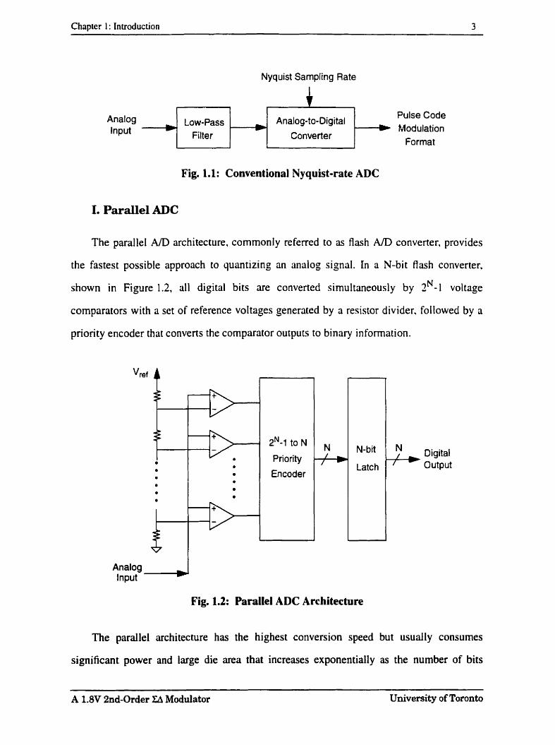
In Nyquist-rate converters the sampling frequency equals the signal Nyquist rate, i.e.
twice the input signal bandwidth. When used in conventional mode, as illustrated in
Figure 1.1, a low-pass analog filter is needed to attenuate high frequency noise and out-of-
band components that alias into the input signal. The three basic types of the Nyquist-rate
converter are: the paraIlel, the serial and the subranging converter.
- - --
A 1.8V 2nd-Order ZA Modulator University of Toronto
Chapter 1 : Introduction 3
Nyquist Sarnpling Rate
Fig. 1.1: Conventional Nyquist-rate ADC
Analog Low-Pass Input Filter
1. Parallel ADC
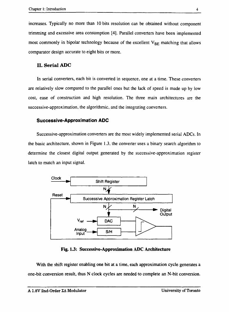
The parallel A/D architecture, commonly referred to as flash A/D converter, provides
the fastest possible approach to quantizing an analog signal. In a N-bit flash converter,
shown in Figure 1.2. al1 digital bits are converted sirnultaneously by 2*-I voltage
comparators with a set of reference voltages generated by a resistor divider. followed by a
ptiority encoder that converts the cornparaior outputs to binary information.
Analog-to-Digital Converter
Pulse Code * Modulation
Format
Digital ++ Output O
O
O
O
Analog & Input
Fig. 1.2: Parallel ADC Architecture
O
O
The parailel architecture has the highest conversion speed but usually consumes
significant power and large die area that increases exponentially as the number of bits
zN-1 to N
Priority
Encoder
-- -
A 1.8V 2nd-Order ZA Modulator University of Toronto
Chapter 1 : Introduction 4
increases. Typically no more than 10 bits resolution cm be obtained without component
trimming and excessive area consumption [4]. Pardlel converters have been implemented
most commonly in bipolar technology because of the excellent VBE matching that allows
comparator design accurate to eight bits or more.
II. Serial ADC
In serial converters, each bit is converted in sequence. one at a time. These converten
are relatively slow compared to the parallel ones but the lack of speed is made up by low
cost, ease of construction and high resolution. The three main architectures are the
successive-approximation, the algorithrnic. and the in tegrat ing converters.
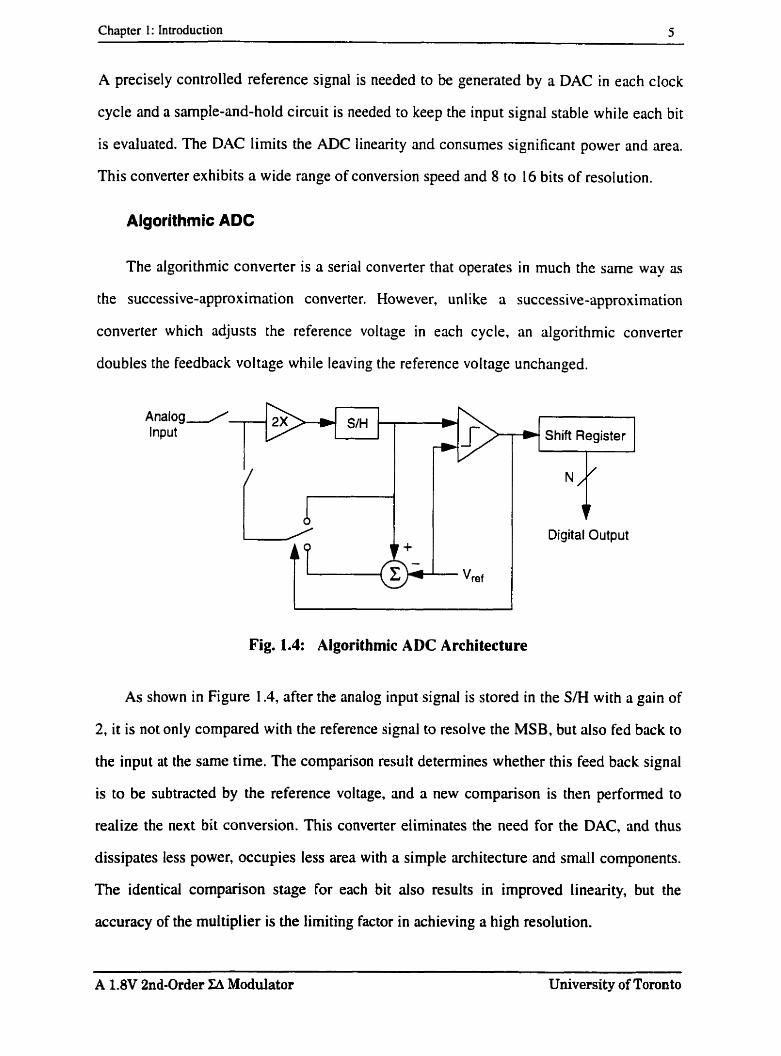
Successive-Approximation AOC
Successive-approximation converters are the most widel y irnplernen ted serial ADCs. In
the basic architecture. shown in Figure 1.3. the converter uses a binüry search algorithm to
determine the closest digital output generated by the successive-approximation register
latch to match an input signal.
Clock Shift Register
Reset 1 Successive Approximation Register Latch
1
Digital Output
Analog input + S/H -
Fig. 1.3: Successive-Approximation ADC Architecture
With the shift register enabling one bit at a time, each approximation cycle generates a
one-bit conversion result, thus N dock cycles are needed to complete an N-bit conversion.
A 1.8V 2nd-Order Eî Modulator University of Toronto
Chapter 1 : Introduction 5
A precisely controlled reference signal is needed to be generated by a DAC in each clock
cycle and a sample-and-hold circuit is needed to keep the input signal stable while each bit
is evaluated. The DAC limits the ADC linearity and consumes significant power and area.
This converter exhibits a wide range of conversion speed and 8 to 16 bits of resolution.
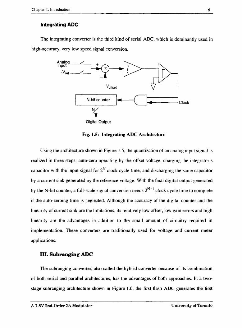
Algorithrnic ADC
The algorithmic converter is a serial converter that operates in much the same way as
the successive-approximation converter. However, unlike a successive-approximation
converter which adjusts the reference voltage in each cycle, an algorithmic converter
doubles the feedback voltage while leaving the reference voltage unchanged.
Shift Register w Nf
Digital Output
Fig. 1.4: Algorithmic ADC Architecture
As shown in Figure 1.4, after the analog input signal is stored in the SM with a gain of
2, it is not only compared with the reference signal to resolve the MSB. but also fed back to
the input at the s m e time. The comparison result determines whether this feed back signal
is to be subtracted by the reference voltage, and a new comparison is then performed to
realize the next bit conversion. This converter eliminates the need for the DAC, and thus
dissipates less power, occupies less area with a simple architecture and srnall components.
The identicai comparison stage for each bit also results in improved linearity, but the
accuracy of the multiplier is the limiting factor in achieving a high resolution.
-- -
A 1.8V 2nd-Order Eî Modulator University of Toronto
Chapter 1 : Introduction 6
Integrating ADC
The integrating converter is the third kind of serial ADC, which is dominantly used in
high-accuracy, very low speed signal conversion.
Analog Input
-"wf
J
N-bit counter 4 Clock
I
Digital Output
Fig. 1.5: Integrating ADC Architecture
Using the architecture shown in Figure 1 S. the quantization of an analog input signal is
realized in three steps: auto-zero operating by the offset voltage, charging the integrator's
capacitor with the input signal for zN clock cycle time, and discharging the sarne capacitor
by a current sink generated by the reference voltage. With the final digital output generated
by the N-bit counter, a full-scale signal conversion needs 2Nf l clock cycle tirne to cornplete
if the auto-zeroing time is neglected. Although the accuracy of the digital counter and the
linearity of current sink are the limitations, its relatively low offset, low gain errors and high
linearity are the advantages in addition to the small arnount of circuitry required in
implementation. These converters are traditionally used for voltage and current meter
applications.
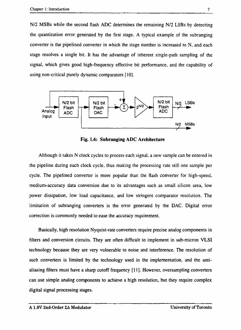
III. Subranging ADC
The subranging converter, also called the hybrid converter because of its combination
of both serial and parallel architectures, has the advantages of both approaches. In a two-
stage subranging architecture shown in Figure 1.6, the first flash ADC generates the first
- - - - --
A 1.8V 2nd-Order E% Modulator University of Toronto
Chapter 1 : Introduction 7
N/2 MSBs while the second flash ADC determines the remaining N/2 LSBs by detecting
the quantization error generated by the first stage. A typical example of the subranging
converter is the pipelined converter in which the stage number is increased to N, and each
stage resolves a single bit. It has the advantage of inherent single-path sampling of the
signal, which gives good high-frequency effective bit performance, and the capability of
using non-critical purely dynamic comparators [10].
Flash
NI2 MSBs
Flash Analog input
- Fig. 1.6: Subranging ADC Architecture
N/2 bit Flash ADC
Although it takes N ciock cycles to process each signal. a new sample can be entered in
the pipeline during each clock cycle, thus making the processing rate stili one sarnple per
cycle. The pipelined converter is more popular than the Rash converter for high-speed,
medium-accuracy data conversion due to its advantages such as srnall silicon area, low
power dissipation. low Ioad capacitance, and lûw stringent cornparator resolution. The
limitation of subranging converters is the error generated by the DAC. Digital error
correction is commonly needed to easc the accuracy requirement.
Basically, high resolution Nyquist-rate converters require precise analog components in
filters and conversion circuits. They are often difficult to implement in sub-micron VLSI
technology because they are very vulnerable to noise and interference. The resolution of
such converters is lirnited by the technology used in the implementation, and the anti-
aliasing filters must have a sharp cutoff frequency [ 1 11. However, oversarnpling converten
can use simple analog components to achieve a high resolution, but they require complex
digital signal processing stages.
A 1.8V 2nd-Order ZA Modulator University of Toronto
Chapter 1 : Introduction 8
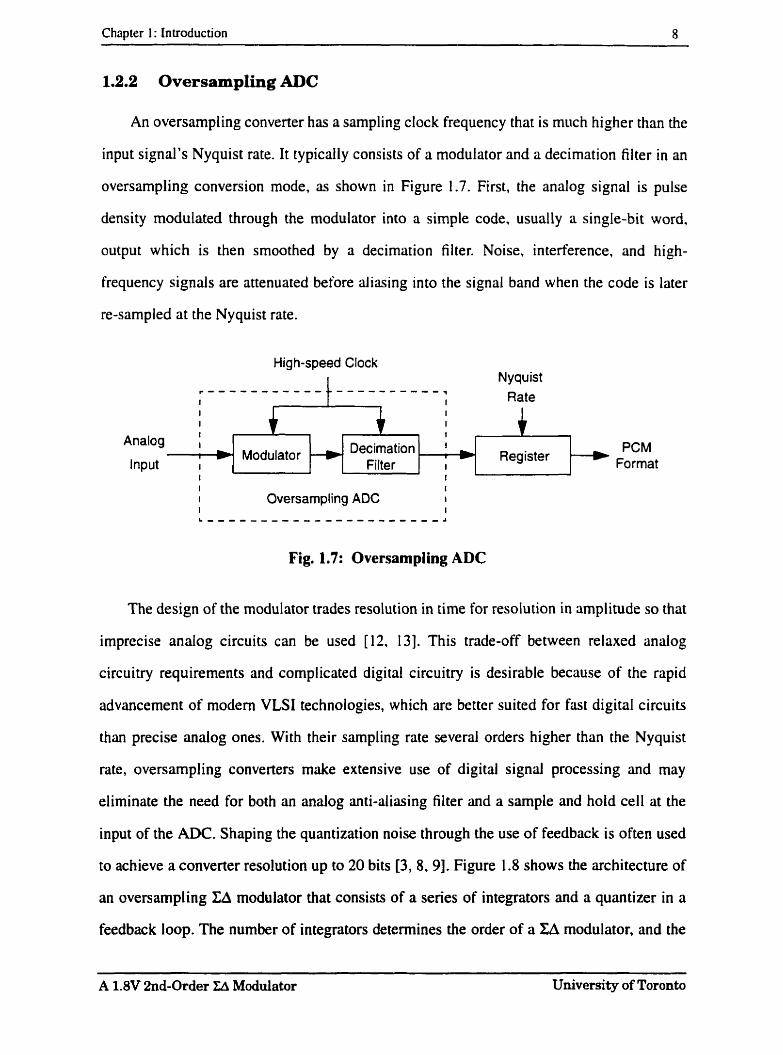
1.2.2 Oversampling ADC
An oversarnpling converter has a sarnpling clock frequency that is much higher than the
input signal's Nyquist rate. It typically consists of a modulator and a decimation filter in an
oversampling conversion mode, as shown in Figure 1.7. First, the analog signal is pulse
density modulated through the modulatot into a simple code, usually a single-bit word,
output which is then smoothed by a decimation filter. Noise, interference, and high-
frequency signals are attenuated before aliasing into the signal band when the code is later
re-sampled at the Nyquist rate.
Nyquist
I 1 I I
Analog f 1
l Modulator --) l Register Decimation PCM Input I Filter I Format
t f
Fig. 1.7: Oversampling ADC
The design of the modulator trades resolution in time for resolution in amplitude so that
imprecise analog circuits can be used [12, 131. This trade-off between relaxed analog
circuitry requirements and complicated digital circuitry is desirable because of the rapid
advancement of modem VLSI technologies, which are better suited for fast digital circuits
than precise anaiog ones. With their sampling rate several orders higher than the Nyquist
rate, oversampling converten make extensive use of digital signal processing and may
eliminate the need for both an analog anti-aliasing filter and a sample and hold ce11 at the
input of the ADC. Shaping the quantization noise through the use of feedback is often used
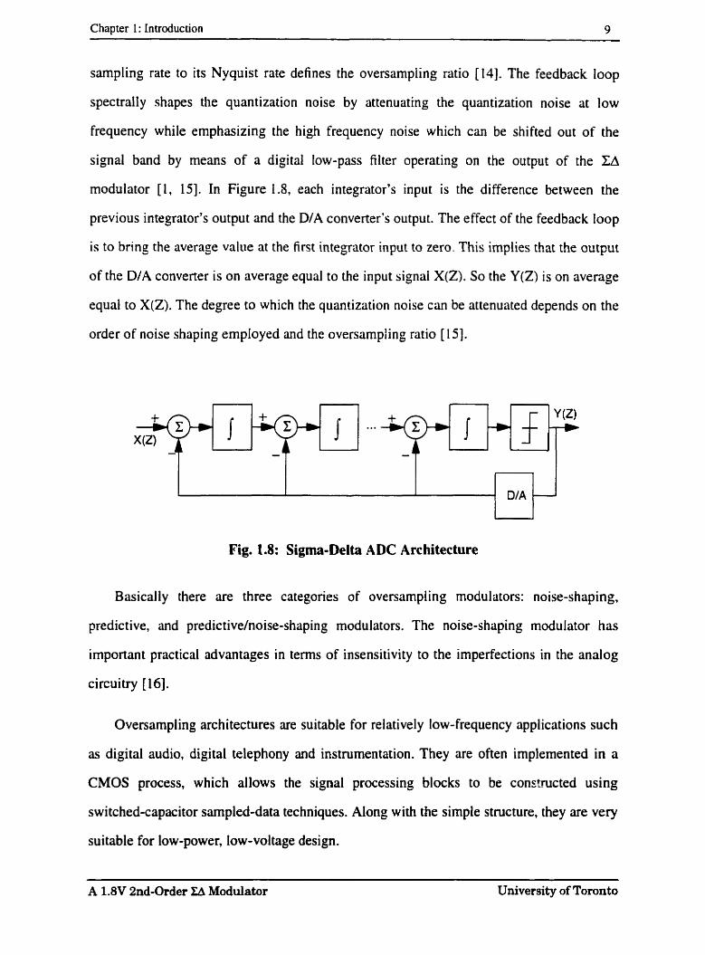
to achieve a converter resolution up to 20 bits [3, 8,9]. Figure 1.8 shows the architecture of
an oversampling ZA modulator that consists of a series of integrators and a quantizer in a
feedback loop. The number of integrators determines the order of a ZA modulator, and the
A 1.8V 2nd-Order ZA Moduiator University of Toronto
Chapter 1 : Introduction 9
sampling rate to its Nyquist rate defines the oversampling ratio [14]. The feedback loop
spectrally shapes the quantization noise by attenuating the quantization noise at low
frequency while emphasizing the high frequency noise which can be shifted out of the
signal band by means of a digital low-pass filter operating on the output of the ZA
rnodulator [ l , 151. In Figure l .S, each integrator's input is the difference between the
previous integrator's output and the D/A converter's output. The effect of the feedback Ioop
is to bring the average value at the first integrator input to zero. This implies that the output
of the D/A converter is on average equal to the input signal X(Z). So the Y(Z) is on average
equal to X(Z). The degree to which the quantization noise can be attenuated depends on the
order of noise shaping employed and the oversampling ratio [ 151.
Fig. 1.8: Sigma-Delta ADC Architecture
Basically there are three categories of oversampling modulators: noise-shaping,
predictive, and predictivehoise-shaping modulators. The noise-shaping modulator has
important practical advantages in tems of insensitivity to the imperfections in the analog
circuitry [16].
Oversampling architectures are suitable for relatively low-frequency applications such
as digital audio. digital telephony and instrumentation. They are often implemented in a
CMOS process, which allows the signal processing blocks to be conntnicted using
switched-capacitor sampled-data techniques. Along with the simple structure, they are very
suitable for low-power, low-voltage design.
A 1.8V 2nd-Order ZA Modulator University of Toronto
Chapter 1 : Introduction IO
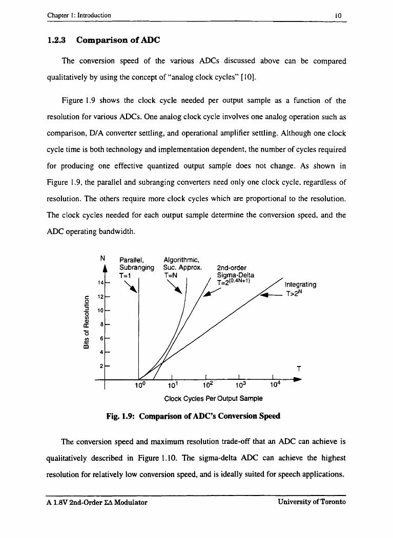
1.2.3 Comparison of ADC
The conversion speed of the various ADCs discussed above can be compared
qualitatively by using the concept of "analog dock cycles" [IO].
Figure 1.9 shows the clock cycle needed per output sample as a function of the
resolution for various ADCs. One anaiog clock cycle involves one analog operation such as
cornparison, DIA converter settling, and operational amplifier settling. Although one clock
cycle time is both technology and implementation dependent. the number of cycles required
for producing one effective quantized output sample does not change. As shown in
Figure 1.9. the parallrl and subranging converters need only one clock cycle. regardless of
resolution. The others require more clock cycles which are proportional to the resolution.
The clock cycles needed for each output sample detenine the conversion speed. and the
ADC operating bandwidth.
N Parallel. Algorithmic, Subranging Suc. Approx. 2nd-order
c 12- O .- œ
2 10- O cn
ic.
O s 6- c1
4 - T
Clock Cycles Per Output Sample
Fig. 1.9: Comparison of ADC's Conversion Speed
The conversion speed and maximum resolution trade-off that an ADC can achieve is
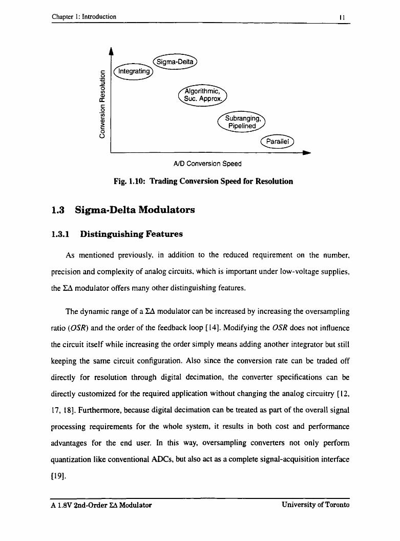
qualitatively described in Figure 1.10. The sigma-delta ADC can achieve the highest
resolution for relatively low conversion speed, and is ideally suited for speech applications.
.- - - - - -
A 1.8V 2nd-Order ZA Moddator University of Toronto
Chapter 1 : Introduction 1 1
N D Conversion Speed
Fig. 1.10: Trading Conversion Speed for Resolution
1.3 Sigma-Delta Modulators
1.3.1 Distinguishing Features
As mentioned previously, in addition to the reduced requirement on the number,
precision and complexity of analog circuits. whic h is important under Iow-voltage supplies,
the ZA modulator offers many other distinguishing features.
The dynamic range of a ZA modulator can be increased by increasing the oversampling
ratio (OSR) and the order of the feedback loop [14]. Modifying the OSR does not influence
the circuit itself while increasing the order simply means adding another integrator but still
keeping the same circuit configuration. Also since the conversion rate can be traded off
directly for resolution through digital decimation, the converter specifications can be
directly customized for the required application without changing the analog circuitry [12,
17, 181. Furthemore, because digital decimation can be treated as part of the overall signal
processing requirements for the whole system, it results in both cost and performance
advantages for the end user. In this way, ovenampling converters not only perforrn
quantization Iike conventional ADCs, but also act as a complete signal-acquisition interface
~ 9 1 .
A 1.8V 2nd-Order ZA Modulator University of Toronto
Chapter 1 : Introduction 12
The ZA modulator simplifies the requirement placed on the analog anti-aliasing filter
because of the high rate of oversampling. A continuous-time anti-aliasing Alter for an
oversampling converter is still necessary, but only for anti-aliasing protection against the
high initial sampling rate. The large difference between the desired signal bandwidth and
the new anti-aliasing cut-off frequency means that the available transition bandwidth for the
filter is many times its passband width. and this makes it much easier to realize the anti-
aliasing filter with low precision andog circuitry. The oversampled signal must be further
filtered to suppress lrequencies higher than half of the Nyquist frequency. but this occurs
digitally after the signal has been quantized [4, 191.
By using single-bit quantization within the ferdback loop. a ZA modulator yields low
distortion and high linearity conversion in that an in-loop 1 -bit DAC only has two output
values. Since two points define a straight line, no trimming or calibration is required for the
1 -bit DAC [8. 201. Along with the oversampling rates, a ZA modulator greatly improves the
ADC's resolution on the accuracy available from circuit rlement matching in a Nyquist-rate
converter [2 1 1.
The ZA modulator offers a power-efficient way of implementing a high-resolution N D
converter because much of the signal processing occurs in the digital domain where power
consumption can be dramatically reduced simply by scaling the technology and reducing
the voltage supply [ l , 7,221. The relaxed requirernents for the analog anti-aliasing filter also
represent a significant power dissipation advantage in cornparison with N y q ~ . '1st-rate
converters [5,23].
By oversarnpling and noise-shaping, the ZA modulator is more robust against circuit
imperfections than conventionai quantizers because the signal binary quantizer is less
sensitive to circuit mismatch and precision (19,241.
- - - - - -- - . .
A 1.8V 2nd-Order Eî Modulator University of Toronto
Chapter 1 : Introduction 13
Although the digital signal processing stage is an expense associated with using a ZA
modulator, the dramatic down-scaling of digital circuits coupled with the optimized design
of infinite impulse response (W) filters can result in greatly reduced die area for decimating
and interpoiating filters [25].
However, sorne problems rernain when implementing a LA converter. The quantization
noise is actually signal dependent and not statistically uncorrelated as is usually assumed.
This results in reduced performance. especially in low-order modulators. High-order XA
modulators make the quantization noise less signal dependent and cause higher effective
resolution to be achieved for the same oversampling ratio, but they suffer from instability
problems [24]. A higher oversampling ratio leads to a higher resolution, but results in more
power consumption [22]. Compared with the parailel architectures. the ZA modulator also
has a limited bandwidth due to oversampling.
Al1 these features make the ZA modulator appea
frequency audio applications [ 1 7,261.
ling for high-resolution, relative
1.3.2 Architecture Trade-offs
For a range of applications, a variety of EA modulator architectures have been
suggested, which can be classified as either single-loop or multi-stage types [9. 23, 271. The
single-loop uses one quantizer and a DIA converter dong with a series of integrators while
the multi-stage consists of a cascade of single-loop LA modulators. Both architectures can
employ either single-bit or multi-bit quantizers and combined D/A converters [14]. High
order single-loop architectures suffer frorn potential instability owing to the accumulation
of large signals in the integrators [ l , 281. Cascade architectures use combinations of
inherently stable low order single loops to achieve higher order noise-shaping, but the
constraints on circuit imperfection and mismatch will be more severe [l, 14, 201.
Combining multi-bit D/A converters results in reduced quantization noise, improved
A 1.8V 2nd-Order Xiî Modulator Uaiversity of Toronto
Chapter 1: Introduction 14
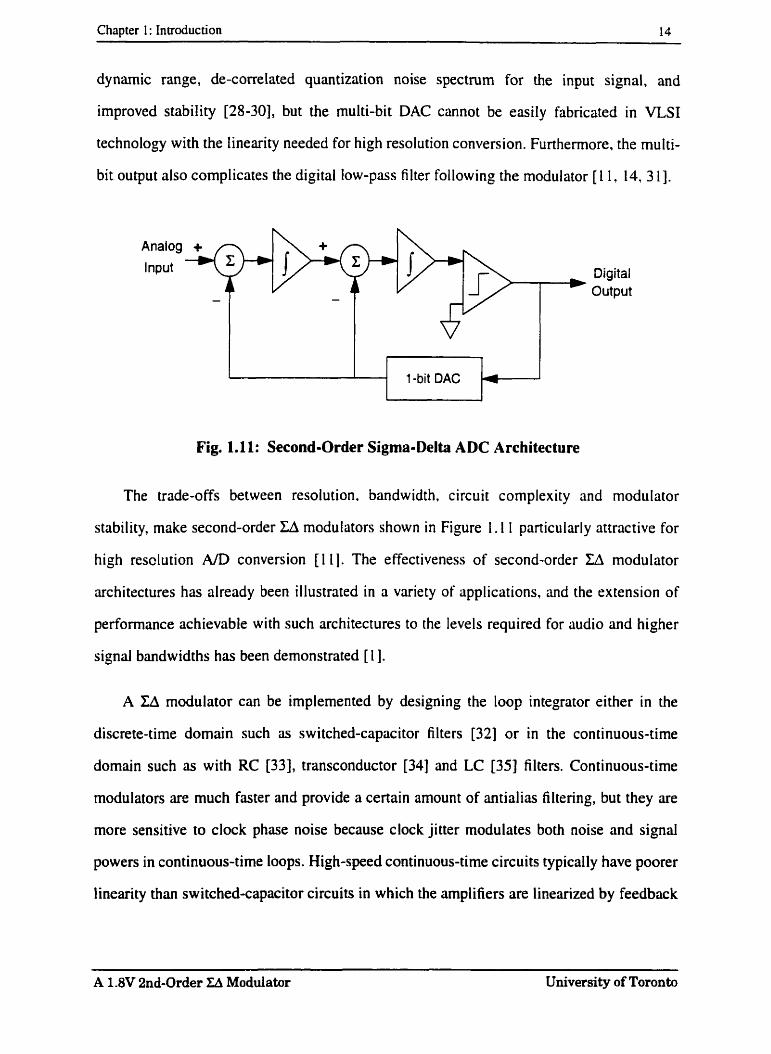
dynarnic range, de-correlated quantization noise spectrum for the input signal, and
irnproved stability [28-301, but the rnulti-bit DAC cannot be easily fabricated in VLSI
technology with the linearity needed for high resolution conversion. Funhermore. the multi-
bit output also complicates the digital low-pas filter following the modulator [ l 1, 14, 3 11.
Digital * Output
Fig. 1.1 1: Second-Order Sigma-Delta ADC Architecture
The trade-offs beiween resolution. bandwidth. circuit complexity and modulator
stability, make second-order ZA modulators shown in Figure 1.1 1 particularl y attractive for
high resclution A/D conversion [I 11. The effectiveness of second-order ZA modulator
architectures has already been illustrated in a variety of applications, and the extension of
performance achievable with such architectures to the levels required for audio and higher
signal bandwidths has been demonstrated [Il.
A ZA rnodulator can be implemented by designing the loop integrator either in the
discrete-time domain such as switched-capacitor filters [32] or in the continuous-time
domain such as with RC [33], transconductor [34] and LC [35] filten. Continuous-time
modulators are much faster and provide a certain amount of antialias filtering, but they are
more sensitive to clock phase noise because clock jitter modulates both noise and signal
powers in continuous-tirne loops. High-speed continuous-time circuits typicall y have poorer
linearity than sw itched-capacitor circuits in which the amplifiers are linearized by feedback
A 1.8V 2nd-Order XA Modulator University of Toronto
Chapter 1: Introduction 15
and pulse shapes during settling have no effect on the final output [36]. At present, most
reported ZA modulators are implemented using switched-capacitor techniques [36,37].
1.4 Previous Work on Low-Voltage ZA Modulator
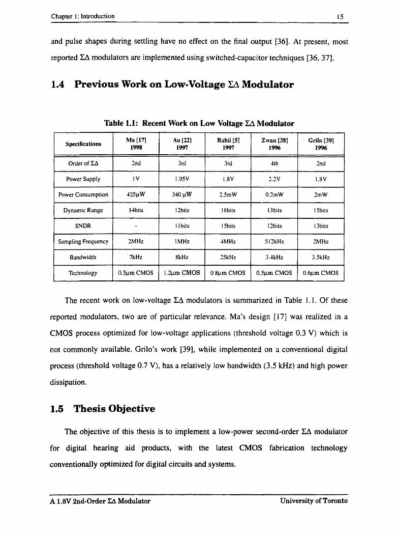
Table 1.1: Recent Work on Low Voltage Zâ Modulator
Ma [IV Au [22] S peci fica tions Rabii [51 Zwan [38] Grilo [391 1 1998 1996
The recent work on low-voltage Id modulators is summarized in Table 1.1. Of these
reported moduIators. two are of particular relevance. Ma's design [17] was realized in a
CMOS process optimized for low-voltage applications (threshold voltage 0.3 V) which is
not commonly available. Grilo's work [39], while implemented on a conventional digital
process (threshold voltage 0.7 V), has a relatively low bandwidth (3.5 kHz) and high power
dissipation.
Order of LA
Power Supply
Power Cansumption
Dy namic Range
SNDR
Srimpling Frequrncy
Brindwidth
Technology
1.5 Thesis Objective
The objective of this thesis is to implement a low-power second-order LA modulator
for digital hearing aid products, with the latest CMOS fabrication technology
conventionally optimized for digital circuits and systems.
2nd
1V
425pW
l Jbits
?MHz
7kHz
OSpm CMOS
- - . -. . -
A 1.8V 2nd-Order ZA Modulator University of Toronto
3rd
1.95'4
340 pW
I2bits
l l bits
l MHz
8kHz
1 .2pm CMOS
4th
1.2V
0.2mW
13bits
12bits
5 1 ?kHz
3.4kHz
0Spm CMOS
I
3 rd
1.8V
2.5rnW
16bits
15bits
JMHz
25kHz
0.8pm CMOS
2nd
1.8V
Zm W
15bits
13bits
?MHz
3SkHz
0.6pm CMOS

Chapter t : Introduction 16
The TSMC 3.3 V, 0.35pm CMOS technology is used for the implementation. With a
threshold voltage around 0.7 V, a single 1.8 V power supply voltage is used to make the
design suitable for electronic systems supplied by two nickel-cadmium or alkaline ce11
batteries in series, while achieving a dynamic range of 15 bits. an input bandwidth of 8 kHz,
and a power dissipation less than 1 milliwatt.
Unlike most of the previous low-voltage reported designs. this design is intended to
include al1 the circuit elements on a single chip. The chip pins are only dedicated for the
power supply, clock signal. analog inputs and digital outputs. Input common-mode voltage
is assumed to be halfway between the power-supply voltages instead of analog ground in
such a way to provide an easier interface with other IC components. As a result, the power
dissipation is minimum, the number of off-chip components is dramatically reduced. and
the efficiency, flexibility and compatibility of the circuit are improved.
Chapter 2 discusses the theory and design concepts of a second-order ZA modulator.
Not only the oversampling and noise-shaping theory are explained and dernonstrated by
high-level simulation techniques, but also the key design principles and trade-off
considerations are described in detail. Al1 the building blocks' specifications, including the
integrator cell design requirements, are discussed.
Chapter 3 presents the transistor level design of the building blocks including the
biasing, the operational-amplifier, the comparator and the clock generator. Circuit,
simulation results and Iayout implementation of each block are discussed as well as the final
realization of the second order LA modulator. Test results of the final experimental
implementation are also reported.
Chapter 4 provides conclusions and suggestions for future work.
A 1.8V 2nd-Order Lî Modulator University of Toronto
Chapter 1 : Introduction 17
References B. Boser and B. Wooley, "The Design of Sigma-Delta Modulator Analog-to-Digital Converters," ZEEE Journal of Solid-Stute Circuits, Vol. 23, pp. 1 298- 1308, 1988.
K. C. H. Chao, S. Nadeem, W. L. Lee, C. G. Sodini, "A High Order Topology for Inter- polative Modulators for Oversampling AID Converters", IEEE Transactions on Cir- cuits und Systems, Vol. 37. pp. 309-3 1 8, 1990.
E. T. King, A. Eshraghi, 1. Galton, and T. S. Fiez, "A Nyquist-Rate Delta-Sigma N D Converter", IEEE Jownnl ofSolid-State Circuits. Vol. 33, pp. 45-52, 1998.
E. A. Vittoz, "Future of Analog in the VLSI Environment", IEEE Joiîmd of Sulid-Sture Circuits, Vol. 23, pp. 1372-1375, 1990.
S. Rabii, and B. A. Wooley, "A 1.8V Digital-Audio Sigma-Delta Modulator in 0.8um CMOS," IEEE Journal of Solid-State Circuits, Vol. 32, pp. 783-795, 1997.
A. K. Ong, and B. A. Wooley, "A Two-Path Bandpass Sigma-Delta Modulator for Dig- ital IF Extraction at 20 MHz", IEEE Jo~trnai ofSolid-State Circuits, Vol. 32, pp. 1920- 1933, 1997.
C. A. T. Salama, "LPLV Limitations, Impact on Device and Process Design". Micronet Course or1 'Low Voltage Low Power Integrgrated Circriit Design ', Course Notes. Toronto. Ontario, Canada, June 1996.
K. Martin and D. Johns. Analog Integrated Circuit Design, John Wiiey & Sons. Inc., Toronto, Canada, 1997.
S. R. Norsworthy, R. Schreier, and G. C. Ternes, Delta-Sigma Data Converters, IEEE Press, IEEE, New York, 1996.
[IOIT. B. Cho, D. W. CLine. C. S. G. Conroy, and P. R. Gray, "Design Considerations for High-Speed Low-Power Low-Voltage CMOS Anaiog-to-Digital Converters", Research Report, University of Califomia at Berkeley, 1991.
(1 11 P. M. Aziz, H. V. Sorensen, and J . V. D. Spiegel, "An Overview of Sigma-Delta Modu- lators", IEEE Signal Processing Magazine, Vol. 13, pp. 6 1-84, 1996.
[12] R. Norsworthy, 1. G. Post, and H. S. Fetterman, "A 14-bit 80-kHz Sigma-Delta A/D Converter: Modeling, Design, and Performance Evduation,*' IEEE Journal of Solid- State Circuits, Vol. 24, pp. 256-265, 1989.
[13] A. M. Marques, V. Peluso, M. S. J. Steyaert, W. Sansen, "A 15-b Resolution 2-MHz Nyquist-Rate Sigma-Delta ADC in a 1-pm CMOS Technology", IEEE Jolirnal of Solid-State Circuits, Vol. 33, pp. 1065- 1075, 1998.
[ 141 A. R. Feldman, High-Speed bw-Power Sigma-Delta Modulators for R F baseband Channel Applications, Ph.D. Thesis, University of Califomia at Berkeley, 1997.
A 1.8V 2nd-Order U Modulator University of Toronto
Chapter 1: Introduction 18
[ 151 L. A. Williams. and B. Wooley, "A Third-Order Sigma-Delta Modulator with Extended Dy namic Range", IEEE Journal of Solid-State Circuits, Vol. 29, pp. 1 93-202, 1 994.
[16] A. Marques, V. Peluso, M. S. J. Steyaert, and W. M. Sansen, "Optimal Parameters for Si,ma-Delta Modulator Topologies", IEEE Transactions on Circiiits and Systems, Vol. 45, pp. 1232- 124 1, 1998.
[ 1 71 S. J. Ma, A Low- Poiver Loiv- Voltage Second-Order Sigma-Delta Modulator; M . A.Sc. Thesis. University of Toronto, 1998.
[ 1 81 R. W. Stewart, "An Overview of Sigma-Delta ADCs and DAC Devices", IEE Collo- quium on Oversarnpling and Sigma- Delta Strategies for DSC pp. I 1 I - 1 /9, 1 995.
[19] M. Hauser, "Principles of Oversampling ND Conversion," J. Alrdio Eng. Soc., Vol. 39, pp. 3-26, 1996.
[?OIS. Chuang, H. N. Liu, X. G. Yu, T. L. Sculley, and R. H. Barnberger. "Design and Irnplementation of Bandpass Delta-Sigma Modulators Using Hal f-Delay Integrators", IEEE Transactions on Circuits and Systems. Vol. 45, pp. 535-546. 1998.
[2 11 0. Nys, and R. K. Henderson, "A 19-Bit Low-Power Multibit Sigma-Delta ADC Based on Data Weighted Averaging". IEEE Jonrncil of Solid-State Circuits, Vol. 32, pp . 933- 942. 1997.
[22] S. Au, and B. H. Leung, "A 1.95V 0.34mW 12-b Sigma-Delta Modulator Stabilized by Local feedback Loops", lEEE Joirrnal of Solid-Stcite Circuits. Vol. 32. pp. 321-327. 1997.
[13] R. Farrell, and 0. Feely, "Bounding the lntegrator Outputs of Second-Order Sigma- Delta Modulators", IEEE Transactions or1 Circrrits and Systems. Vol. 45. pp. 69 1 -702, 1998.
[24] R. M. Gray, "Oversampled Sigma-Delta Modulation", IEEE Transactions on Commu- nications, Vol. 35, pp. 48 1-489, 1987.
[25] D. Senderowicz, G. Nicollini, S. Pernici, P. Confalonieri, and C. Dallavalle, "Low Volt- age Double Sampled Sigma-Delta Converters", IEEE Journal of Solid-State Circuits, Vol. 32, pp. 1907-1918, 1997.
[26] K. Khoo, Programmable Higk-Dynamic Range Sigma-Delta AD Converters for Mirlti- standard Fully-lntegrated RF Receivers, M.S. Thesis. University of California at Ber- keley, 1999.
[27] J. C. Candy, G. C. Ternes, Oversampling Delta-Sigma Data Converters, IEEE Press, New York, U.S.A., 1992.
[28] G. Fischer, and A. J. Davis, "Alternative Topologies for Sigma-Delta Modulators - A Comparative Study", IEEE Transactions on Circuits and Systems, Vol. 44. pp. 789-797, 1997.
A 1.8V 2nd-Order ZA Modulator University of Toronto
Chapter 1 : Introduction 19
[29] J. W. Fattaruso, S. Kinaki, M. de Wit, and G. Warwar, "Self-Calibration Techniques for a Second-Order Multi bit S igrna-Delta Modulator," IEEE Journal of Solid-Stare Cir- cuits, Vol. 28, p 12 16- 1223. 1993.
[30] A. Gothenberg, and H. Tenhuen, "Performance Analysis of Low Oversarnpling Ratio Sigma-Delta Noise Shapers for RF Applications," IEEE Internntional Symposium on Circuits and Systems, Vol. 1 , pp. 40 1 -404, 1 998.
[3 !] E. W. Chan, h w Power Aitdio Codec, M.S. Thesis, University of California at Berke- ley, 1997.
[32] S. A. Jantzi, W. M. Snelgrove. and P. F. Ferguson, "A Fourth-Order Bandpass Sigma- Delta Modulator", lEEE loltnial of Solid-Stare Circltits. Vol. 38, pp. 782-29 1, 1993.
[33] J. F. Jensen, G. Raghavan. A. E. Cosand, and R. H. Walden, "A 3.2GHz Second-Order Del ta-Sigma Moduiator Implemented on InP HBT Technology", IEEE Jortmol uf Solid-State Circuits, Vol. 30, pp. 1 1 19- 1 127, 1995.
[34] 0. Shoaei, and W. M. Snelgrove, "Optimal Bandpass Continuous-Time Sigma-Delta Modulator", IEEE International Svmposium on Circuits cind Systems. Vol. 5, pp. 489- 492, 1994.
[35]P. H. Gaiius, W. J. Turney, and R. F. Yester. "Method and Arrangement for a Sigma- Delta Converter for Bandpass Signais", U.S. Patent 4857928. Aug. 15, 1989.
[36) W. Gao, and W. M. Snelgrove, "A 950MHz IF Second-Order Integrated LC Bandpass Delta-Sigma Modulator", IEEE Jorrmal of Solid-State Circuits. Vol. 33, pp. 723-732, 1998.
[37] S. Bazarjani. and W. M. Snelgrove. " A 160MHz Fourth-Order Double-Sarnpled SC Bandpass Sigma-Dei ta Modulator", IEEE Journal of' Solid-Sfute Circuits, Vol. 45, pp. 547-555, 1998.
[38] E. J. van der Zwan, and E. C. Dijkrnans, "A 0.2mW CMOS Sigma-Delta Moduiator for Speech Coding wiih 80dB Dynamic Range," IEEE International Soiid-Stote Circrtits Conference, Digest of Technical Papers, pp. 232-232, 1996.
[39] J. Grilo, E. MacRobbie, R. Halim and G. Ternes, "A 1.8V 94dB Dynamic Range Sigma-Delta Modulator for Voice Applications," IEEE International Solid-State Cir- cuits Conference, Digest of Technical Papers, pp. 230-23 1, 1996.
A 1.8V 2nd-Order Zâ Modulator University of Toronto
Chapter 2: Second-Order Sigma-Delta Modulator 20
CHAPTER 2
Second-Order Sigma-Delta Modulator
2.1 Introduction
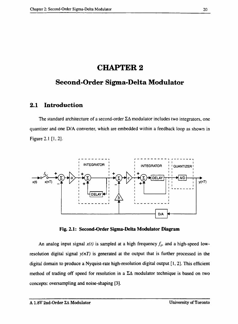
The standard architecture of a second-order ZA modulator includes two integrators, one
quantizer and one D/A converter, which are embedded within a feedback loop as shown in
Figure 2.1 [ 1 .2] .
Fig. 2.1: Second-Order Sigma-Delta Modulator Diagram
An analog input signal x(t) is sampled at a high frequency f,, and a high-speed low-
resolution digital signal y(nT) is generated at the output that is further processed in the
digital domain to produce a Nyquist-rate high-resolution digital output [ l , 21. This efficient
method of trading off speed for resolution in a ZA modulator technique is based on two
concepts: oversampling and noise-shaping [3].
A 1.8V 2nd-Order ZA Modulator University of Toronto
Chapter 2: Second-Order Sigma-Delta Modulator 2 1
2.2 Oversampling and Noise-Shaping
Oversampling reduces the quantization noise power in the signal band by spreading a
fixed quantization noise power over a bandwidth that is much larger than the signal band,
while noise-shaping further attenuates this noise in the signal band and amplifies it outside
the signal band [3.4,5].
2.2.1 Oversampling
Oversampling theory is based on an exact quantization model that the output quantized
signal y(n) is the sum of the input signal value x(n) and the quantization error e(n). which is
strongly related to the input signal. For a rapidly and randomly active input signal x(n), r ( n )
can be assumed to be a statistically uncorrelated white-noise signai. Ieading to an
approximate quantizer model with reasonably accurate results [6. 71.
In an ovenampling converter, the same noise power produced as a Nyquist-rate
converter is uniformiy distributed between -J,/2 and f J 2 , where A is the sampling
frequency. Because f, is much greater than the signal Nyquist-rate and the overall
quûntization error energy is constant, only a small fraction of the total noise power falls in
the signal band, which is given by 17, 8.91
A? 2 f b AI 1 pE = [g. I ) ~ ~ = - . - = -. -,
-fb 12 f s 12 f s 12 OSR
where OSR is the oversarnpling ratio, fb is the signal bandwidth. A ~ / I 2 is actually the
quantization noise power of a Nyquist converter where A is the quantizer step size.
For an N-bit quantizer with 2N quantization levels, the maximum signal power equals
A 1.8V 2nd-Order ZA Modulator University of Toronto
Chapter 2: Second-Order Sigma-Delta Modulator 22
Thus the maximum signal-to-noise ratio of an oversampling converter is given by
SNR,,, = I0log(5) = 6.O?N + 1.76 + IOlog(OSR) PE
The last term is the SNR increment due to the oversampling, while the sum of the first
two terms represents the SNR resulting from an N-bit quantizer. Increasing the quantizer
bit-resolution N and the oversampling ratio OSR results in an enhanced SNR. However.
when taking the advantage of the inherent linearity of a 1-bit quantizer (N = 1) , the
oversampling alone usually cannot make the SNR high enough with a practical sampling
rate. For efficiency, noise-shaping needs to be introduced to help achieve a high resolution.
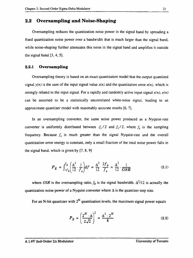
2.2.2 Noise-Shaping
Using the feedback loop configuration illustrated in Figure 2.2, noise-shaping in a XA
modulator increases the baseband signal-to-noise ratio by virtue of attenuating quantization
noise at low frequencies [5, 71.
Fig. 2.2: Modulator Linear Model
Treating this modulator linear mode1 under the assumption that x(n) and e(n) are the
two independent inputs, the corresponding output signal transfer function in frequency
domain can be described by 110, 1 11
A 1.8V 2nd-Order ZA Moddator University of Toronto
Chapcer 2: Second-Order Sigma-Delta Modulator 23
where Fx(Z) and FE(a denote the signal and the noise transfer functions. With a single
loop filter H(Z). they are given by [1 I l
To eliminate noise in the signal base-band. FdZ) should be a high-pass transfer
function, which implies a low-pass H(Z) because the poles of H(Z) are the zeros of FdZ).
When H(Z) is chosen to be a typical unity-gain discrete-time integrator as described in
Equation (2.7), FAZ) tums out to be the Z-trûnsform expression of a pure delay, while
FdZ) is a first-order high-pass response. The output signal transfer function is given by
Equation (2.8) [3. 5. 151.
Y(Z) = Z-' . X(Z) + ( 1 -2-') E(Z) (2.8
This is the realization of first-order noise-shaping with the maximum SNR given by
Comparing this result with Equation (2.3) reveals that dou biing the sample rate with the
first noise-shaping will boost the oversampling payoff to 9 dB or 1.5 bits, whereas without
noise-shaping, the payoff is only 3 dB.
Figure 2.3 is the structure of a standard second-order noise-shaping configuration [4].
The input-output reiationship cm be readily denved. and given in Equation (2.10). The
signai transfer function remains the same, whereas the noise transfer function is the square
A 1.8V 2nd-Order ZA Modulator University of Toronto
Chapter 2: Second-Order Sigma-Delta M~dulator 24
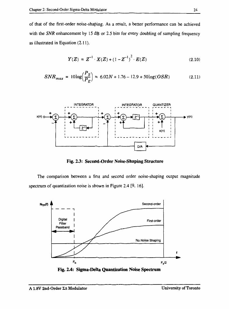
of that of the first-order noise-shaping. As a result, a better performance can be achieved
with the SNR enhancement by 15 dB or 2.5 bits for every doubling of sampling frequency
as illustrated in Equation (2.1 1).
Fig. 23: Second-Order Noise-Shaping Structure
The cornparison between a first and second order noise-shaping output magnitude
spectrum of quantization noise is shown in Figure 2.4 [9, 161.
No Noise Shaping
f
Fb F!P
Fig. 2.4: Sigma-Delta Quantization Noise Spectrum
A 1.8V 2nd-Order ZA Modulator University of Toronto

Chapter 2: Second-Order Sigma-Delta Modulator 25
Since the magnitude of the noise transfer function of a second-order modulator is a
squared sine wave [7.9], the in-band quantization noise contributing to the finite resolution
of the moduiator is further attenuated, while the out-of-band noise is further amplified. The
final digital representation thus gets a higher resolution payoff.
Ideally, an nth-order ZA modulator has an output expressed in Equation (2.4) as a linear
combination of the input signal X(Z) and the quantization error signal E(Z) with the signal
and noise transfer functions FdZ) and FdZ) given by
Basically, higher order noise-shaping leads to lower baseband noise powrr, thus
providing higher signal resolution.
2.3 System-Level Simulation
The objective of this thesis is to design a 15-bit dynamic-range second-order 2 A
modulator. With a 1-bit quantizer, the oversampling ratio can be estimated to be 80 using
Equation (2.9). For audio applications with 8 kHz signal bandwidth. the sampling
frequency tums out to be at l es t 1.28 MHz.
As mentioned before, the linear quantizer model for a ZA modulator has some
approximations based on the assumption that actual signal-dependent quantization noise is
random white noise. With a second-order noise-shaping. the calculation resulting from
Equation (2.9) actually over-estimates the peak SN!? by about 14 dB according to both
Hauser's analysis [11] and Stanley's simulation result 191. To compensate for this
performance reduction, the oversampling ratio needs to be doubled to bring a Further 15 dB
SNR enhancement, so the sampling frequency ends up being 2.56 MHz.
A 1.8V 2nd-Order Li Modulator University of Toronto
Chapter 2: Second-Order Sigma-Delta Modulator 26 -
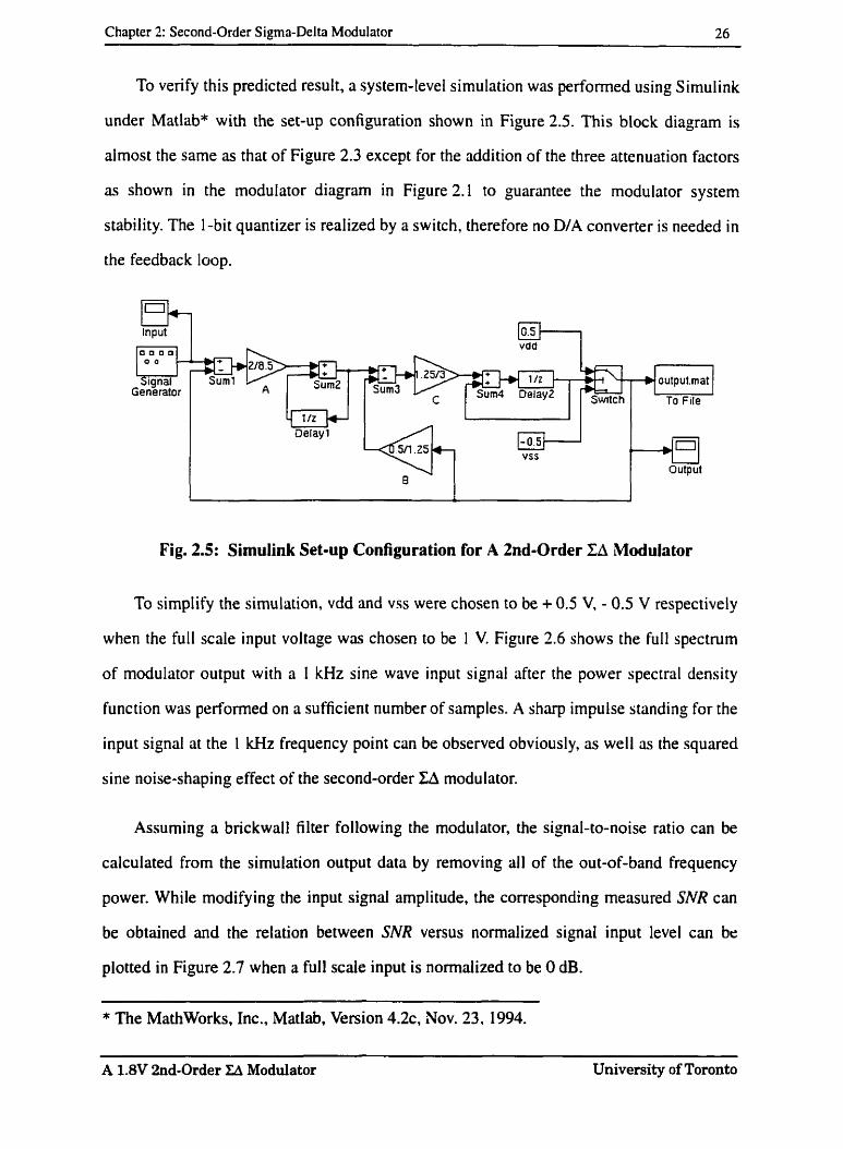
To venfy this predicted result, a system-Ievel simulation was performed using Simulink
under Matlab* with the set-up configuration shown in Figure 2.5. This block diagram is
almost the same as that of Figure 2.3 except for the addition of the three attenuation factors
as shown in the modulator diagram in Figure 2.1 to guarantee the modulator system
stability. The 1 -bit quantizer is realized by a switch, therefore no DIA converter is needed in
the feedback loop.
Input lo]l vdd
pq--1 VSS --el Output
Fig. 2.5: Simulink Set-up Configuration for A 2nd-Order ZA Modulator
To simplify the simulation, vdd and vss were chosen to be + 0.5 V, - 0.5 V respectively
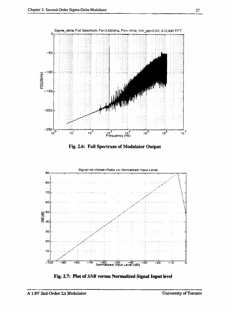
when the full scaie input voltage was chosen to be 1 V. Figure 2.6 shows the full spectrum
of modulator output with a 1 kHz sine wave input signal after the power spectral density
function was performed on a sufficient number of samples. A sharp impulse standing for the
input signal at the 1 kHz frequency point cm be observed obviously, as well as the squared
sine noise-shaping effect of the second-order ZA modulator.
Assuming a brickwall filter following the modulator, the signal-to-noise ratio can be
calculated from the simulation output data by removing al1 of the out-of-band frequency
power. While modifying the input signal amplitude, the conesponding measured SNR can
be obtained and the relation between SNR versus normalized signal input level c m br
plotted in Figure 2.7 when a full scde input is normalized to be O dB.
* The MathWorks, Inc., Matlab, Version 4.2c, Nov. 23, 1994.
A 1.8V 2nd-Order Eî Modulator University of Toronto
Chapter 2: Second-Order Sigma-Delta Modulator 27
/ '
. . . . . . . . . . . . . . . . . . . . . . . . . . . . . . . . . . . . . . . . . . . . . . . . . . . . 3
1 O' l a 2 1 o3 I o4 1 o s 1 o6 10' Frequency (Hz)
Fig. 2.6: Full S p e c t ~ m of Modulator Output
Signal-to-Nclse-Ratlo vs. Normalked Input Level I 1 1 I I L 1 I
/- y :
1 I I t I I I L I 1 -90 -80
-'O ~ o Z % l z e d ~2;ut &F&de1 -30 -20 - t O O
Fig. 2.7: Plot of SNR versus Normalized Signal Input level
A 1.8V 2nd-Order Modulator University of Toronto
Chapter 2: Second-Order Sigma-Delta Modulator 28
According to the simulation result, with ideal analog components, a 15-bit dynamic
range with 8 W z bandwidth cm be realized by using 1-bit quantizer with a second-order
noise-shaping under the sampling frequency 2.56 MHz. The oversarnpling ratio is 160.
2.4 Modulator Design Considerations
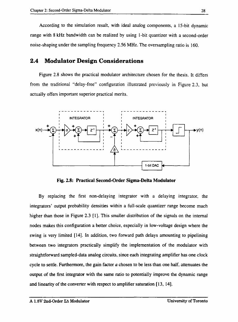
Figure 2.8 shows the pracrical modulaior architecture chosen for the thesis. It differs
frorn the traditional "delay-me" configuration illustrated previously in Figure 2.3, but
actually offers important superior practical merits.
r - - - - - - - - - - - - - 7 r - - - - - - - - - - - - - 1
I I 1 t I INTEGFIATOR I I INTEGRATOR I I 1 I t
Fig. 2.8: Practical Second-Order Sigma-Delta Modulator
By replacing the first non-delaying integrator with a delaying integrator, the
integrators' output probability densities within a full-scale quantizer range become much
higher than those in Figure 2.3 [ l ] . This smaller distribution of the signals on the intemal
nodes makes this configuration a better choice, especially in low-voltage design where the
swing is very limited [14]. In addition. two forward path delays amounting to pipelining
between two integrators practically simplify the implementation of the modulator with
straightforward sampled-data analog circuits, since each integrating amplifier has one dock
cycle to senle. Furthermore, the gain factor a chosen to be less than one half, attenuates the
output of the first integrator with the same ratio to potentially irnprove the dynamic range
and linearity of the converter with respect to amplifier saturation [ 13, 141.
A 1.8V 2nd-Order ZA Modulator University of Toronto
Chapter 2: Second-Order Sigma-Delta Modulator 29
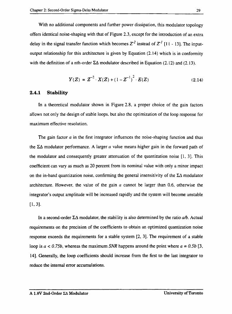
With no additional components and further power dissipation, this rnodulator topology
offers identical noise-shaping with that of Figure 2.3, except for the introduction of an extra
delay in the signal transfer function which becomes 2' instead of Z' [1 I - 131. The input-
output reiationship for this architecture is given by Equation (2.14) which is in conformity
with the definition of a nth-order XA modulator described in Equation (2.12) and (2.13).
2.4.1 Stability
In a theoretical modulator shown in Figure 2.8, a proprr choice of the gain factors
allows not only the design of stable loops, but also the optimization of the loop response for
maximum effective resolution.
The gain factor a in the first integrator influences the noise-shaping function and thus
the XA modulator performance. A larger a value means higher gain in the fonvard path of
the rnodulator and consequently greater attenuütion of the quantization noise [1, 31. This
coefficient can Vary as much as 20 percent from its nominal value with only a minor impact
on the in-band quantization noise, confinning the general insensitivity of the ZA modulator
architecture. However, the value of the gain n cannot be larger than 0.6, otherwise the
integrator's output amplitude will be increased rapidl y and the system wil l become unstable
V , 31.
In a second-order LA modulator, the stability is also determined by the ratio a/b. Actual
requirements on the precision of the coefficients to obtain an optimized quantization noise
response exceeds the requirements for a stable system [2, 31. The requiremcnt of a stable
loop is a < 0.75b. whereas the maximum SNR happens around the point where a = 0.56 [3,
141. Generally, the loop coefficients should increase from the first to the last integrator to
reduce the interna1 error accumulations.
A 1.8V 2nd-Order Modulator University of Toronto
Chapter 2: Second-Order Sigma-Delta Modulator 30
In theory, since the second integrator is followed immediately by a two-level quantizer,
gain factor c can be adjusted arbitrarily without impairing the performance of the modulator
[l]. In practice, c is chosen to make sure that the signais are not clipped in a real
implementation [14].
In switc hed-capacitor integrators, these coefficients are very convenientl y ac hieved by
adjusting the ratio of capacitors to accommodate easier implernentation and better SNR
performance without jeopardizing the modulator stability.
2.4.2 Noise Sources
The performance of a M modulator is not only determined by the in-band quantization
noise as theoretically analyzed in section 2.3, but is also influenced by the circuit noise
associated with solid-state devices in physical implementation. Since the circuit noise
generated in the internai nodes of a ZA modulator loop is strongly suppressed by the high
loop gain, the one injected into the input summing node plays a dominant role. As a result.
the circuit noise of the converter is almost cornpletely determined by the noise of the first
integrator. The main circuit noise sources of a silicon implementation are thermal noise and
flicker noise [14, 17, 181.
1. Thermal Noise
Thermal noise is due to the thermal excitation of charge camers in a conductor. It has a
white spectral density and is proportional to absolute temperature. In a sampled data EA
modulator, the thermal noise is generated by the on-resistance of the switches in the
sarnpling and integrating process. When a fully differential switched-capacitor integrator is
used, the main thermal noise power is given by [18]
4KT 'T = Cs - OSR
-- - -- --
A 1.8V 2nd-order &kodul&r Universi@ of Toronto
Chapter 2: Second-Order Sigma-De! ta Modulator 3 1
where K is Boltzmann's constant, T is the absolute temperature, and Cs is the sampling
capacitance. Obviously, thermal noise cm be diminished by choosing a larger sampling
capacitor or a larger OSR.
II. Flicker Noise
Flicker noise is due to the random trapping and de-trapping of majority camers in the
channel of MOS devices. It is cornmonly referred to as 1 /f noise because the fluctuations in
the channel charge carrier density have a relatively large time constant [7, 81. The
normalized power of a single active MOSFET is given by
where KF is a constant which depends on process characteristics. W and L are the
transistor's width and length respectively. and Cox represents the gate capacitance per unit
area. Typically NMOS devices demonstrate a higher flicker noise than PMOS counterparts
since their majority carriers (electrons) are likely to be trapped [7, 81. As a result. flicker
noise can be diminished mainly by using PMOS as input devices with large device size.
Chopper stabilization and correlated double sampling techniques can also be employed to
provide a firstsrder flicker noise cancellation [S. 14. 181.
In. Noise Contributions
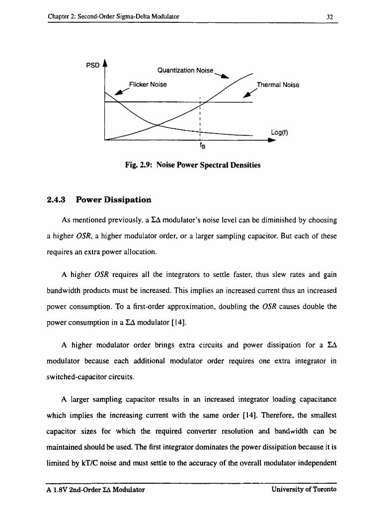
Figure 2.9 represents schematically the different noise levels contributed in a Id
modulator, where fB indicates the signal base-band. The final SNR of a ZA modulator is
determined by the ratio of signal power to both the quantization noise and the circuit noise,
which includes thermal and flicker noise. In practice, quantization noise and thermal noise
are usually the main considerations, whereas Aicker noise can be made low enough with a
careful circuit design so as not to degrade the modulator performance significantly [17].
A 1.8V 2nd-Order ZA Modulator University of Toronto
Chapter 2: Second-Order Sigma-Delta ModuIator 32
Quantizat ion Noise
Fig. 2.9: Noise Power Spectral Densities
2.4.3 Power Dissipation
As mentioned previously. a TA modulator's noise level can be diminished by choosing
a higher OSR, a higher modulator order, or a larger sampling capacitor. But each of these
requires an extra power allocation.
A higher OSR requires al1 the integrators to settle fister, thus slew rates and gain
bandwidth products must be increased. This implies an increased current thus an increased
power consurnption. To a first-order approximation. doubling the OSR causes double the
power consumption in a ZA modulator [ 141.
A higher modulator order brings extra circuits and power dissipation for a ZA
modulator because each additional modulator order requires one extra integrator in
switched-capacitor circuits.
A larger sampling capacitor results in an increased integrator loading capacitance
which implies the increasing current with the same order [14]. Therefore, the srnailest
capacitor sizes for which the required converter resolution and bandividth can be
rnaintained should be used. The first integrator dominates the power dissipation because it is
limited by kT/C noise and must senle to the accuracy of the overall modulator independent
A 1.8V 2nd-Order Eî Modulator University of Toronto
Chapter 2: Second-Order Sigma-Delta Moduiator 33
of OSR. Subsequent integrators may employ smaller capcitors and settle less accurately,
which reduces their power dissipations [19].
Operating at reduced supply voltages is not advantageous from a power dissipation
perspective for analog circuits whose dynamic range is kTIC limited because the capacitor
values need to be increased as the inverse square of the power supply voltage to preserve the
same dynarnic range. This not only cancels any advantage accrued in dynamic power
dominated by C V ~ , but also again implies increased current. But balanced against this
fundamental consideration is the fact that, since analog circuits reside only as a small cell.
in many current mixed-signal systems, large digital portions dominate the overall power
dissipation, which benefits from the combination of scaled technology and reduced supply
voltages.
2.4.4 Switches
The behavior of a switch is of great importance in switched-capacitor circuits because
i t may lirnit both the input signal range and the obtainable operating frequency.
The input signal must be operating in such a range that the driving signal can tum on
the switch at any input signal level. Although in one MOS transistor switch, this range is
limited by the gate driving voltage and the MOS threshold voltage, a CMOS transmission
gate allows the passage of a rail-to-rail input signal, which is thereby an exact choice in
switched-capacitor circuits. The circuit operating frequency is influenced by the time
constant defined by the switch on-resistance together with the sampling capacitor [39]. The
on-resistance should be as small as possible to meet the speed requirement.
The gate dnving voltage plays an important role in the switch performance. Although a
low-supply voltage results in a great power saving for digital circuits, it creates a switch
driving problem for analog switched-capacitor circuits. For a CMOS switch. the gate
driving voltage must be larger than the sum of NMOS threshold voltage VN and PRlOS
- -
A 1.8V 2nd-Order U Moduiator University of Toronto
Chapter 2: Second-Order Sicoma-Delta Modulator 3 4
threshold voltage V p Further consideration of the transistor's body effect requires the gate
driving voltage to be even higher. For a low supply voltage condition where
VDD < VN + VP a bootstrapping circuit using charge pumps must be introduced which cm
increase the driving voltage approximately up to 2VDD [M, 201.
A large on-resistance due to low gate driving voltage can be reduced by increasing the
transistors' width over length ratio. But a larger transistor size induces a larger charge
injection [40]. In CMOS transmission gates. the charge injection can be partially cancelled
because of the opposite charges produced by both NMOS and PMOS transistors. For the
switches used between integrators and comparators in a modulator, the charge injection can
be further significantly reduced by the fully differential configuration and the proper turning
on/off sequences [ 1.7.361.
Linearity is another important factor in the design of the switches. The switches should
operate with a relatively constant on-resistance. independent of the input voltage. In a
CMOS transmission gate. PMOS should be larger than NMOS by a factor around their
rnobility ratio. The fina! choice of switch size is based on the trade-off between the desire to
reduce the senes RC time constant, the switch linearity, and the requirement to keep
parasitic and charge injection eflects negligible [40].
2.4.5 Dynamic Range, SNR and SNDR
When evaluating the performance of a LA modulator, three main related speci fications
are Dynamic range, SNR and SNDR. The dynarnic range of a modulator is defined as the
ratio of the power in a full-scale input to the power of a sinusoidal input for which the
signal-to-noise ratio (SNR) is one. It is the ratio in power between the maximum input signal
level that the rnodulator can handle and the minimum detectable input signal. SNR is the
ratio of the output signal power to the noise power, which includes al1 noise sources in the
modulator. SNDR is the ratio of the output signai power to the sum of the noise and
- - -- - -
A 1.8V 2nd-Order Ziî Moddator Üniversity of Toronto
Chapter 2: Second-Order Sigma-Delta Modulator 35
harmonic distortion powers. For small signal levels, distortion is not important, implying
that the SNR and SNDR are approximately equal. As the signal Ievel increases, the precision
of the converter is limited by harmonic distortion rather than quantization noise. Distortion
degrades the modulator performance, so the SNDR wil1 be less than SNI? [ I l .
In a modulator with performance limited by circuit noise. higher supply voltages
improve the dynamic range due to the increased signal power and a constant thermal noise
floor. For a low-supply voltage design, the input-signal amplitude rnust be maxirnized to
rnaximize the dynamic range. In practice, the maximum input amplitude is typically limited
to a fraction of the feed back reference levels to ensure the stability of a second-order ZA
modülator [l8].
As rnentioned before. coefficients a. b. and c. in Figure 2.8. not only determine the
modulator stability. but also influence the modulaior dynamic range. Peluso [2 1 ] provided a
detailed anal ysis on the topology coefficients that y ield the best performance in terms of
dynamic range. Generally, within the boundaries of stability requirements. ü constant
product of integrator gains yields approximately equal performance. while the maximum
dynamic range is found close to the stability border. In a second-order ZA rnodulator, as
mentioned in section 2.4.3, the coefficients' requirements for an optirnized dynarnic range is
a = 0.56, exceeding those for stability.
2.4.6 Input Full-Scale Range
The choice of a full-scale analog input nnge for the converter involves trade-offs
arnong a number of important design constraints. A large signal range results in a large
dynarnic range 1221, but also an increased harmonic distortion due to the integrator
nonlinearity (11. Increasing the signal range may cal1 for the opamp with slew limiting [23].
To avoid significant performance degradation, the full-scale analog input signal range is
usually smaller than 2 / 3 signai range at the outputs of both integrators [I l .
A 1.8V 2nd-Order Lî Modulator University of Toronto
Chapter 2: Second-Order Sigma-Delta Modulator 36
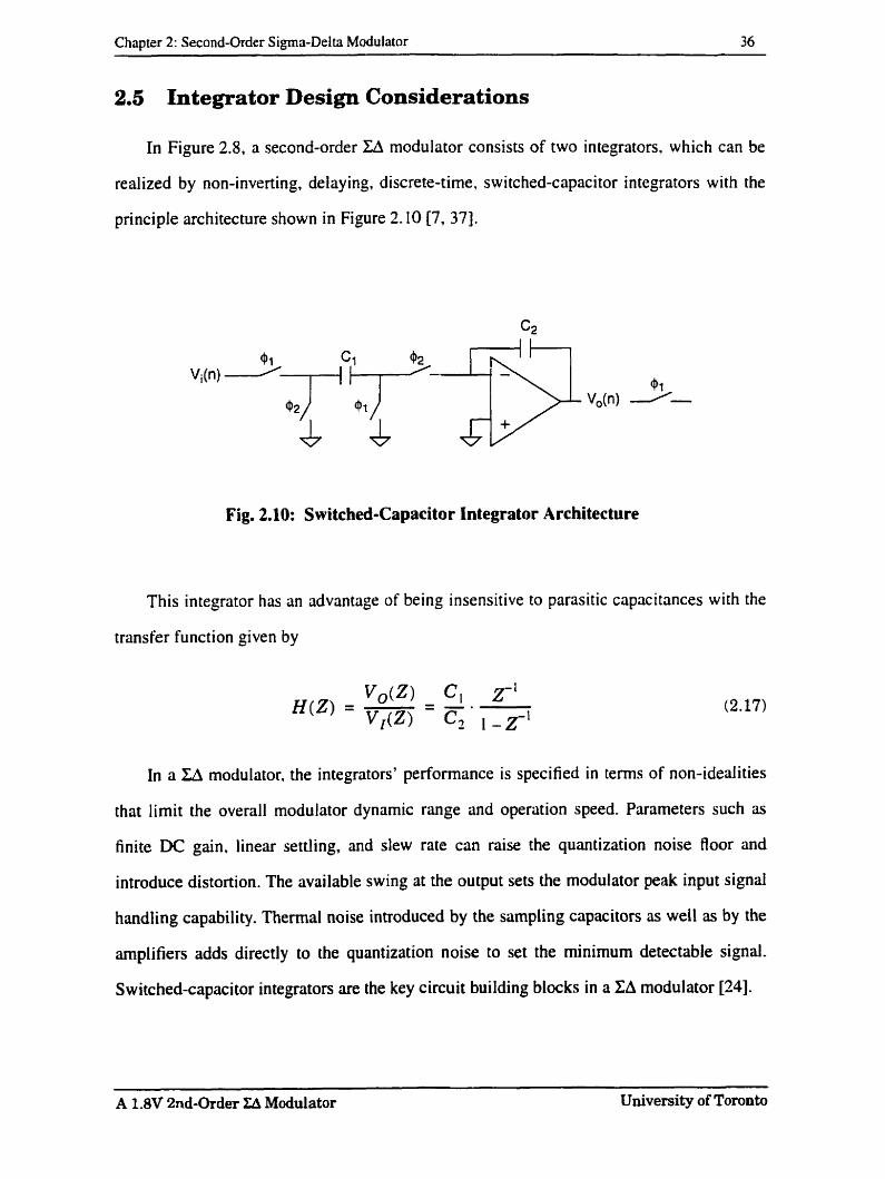
2.5 Integrator Design Considerations
In Figure 2.8, a second-order ZA modulator consists of two integraton, which can be
realized by non-inverting, delaying, discrete-tirne, switched-capacitor integrators with the
principle architecture shown in Figure 2.10 [7, 371.
Fig. 2.10: Switched-Capacitor Integrator Architecture
This integrator has an advantage of being insensitive to parasitic capacitances with the
transfer function given by
In a ZA modulator. the integrators' performance is specified in terms of non-idealities
that limit the overall modulator dynamic range and operation speed. Parameters such as
finite DC gain. linear settling, and slew rate can raise the quantization noise Roor and
introduce distortion. The available swing at the output sets the modulator peak input signal
handling capability. Thermal noise introduced by the sampling capacitors as well as by the
amplifiers adds directly to the quantization noise to set the minimum detectable signal.
Switched-capacitor integrators are the key circuit building blocks in a LA modulator [24].
A ~ Ë v 2nd-Order 2A Modulator University of Toronto

Chapter 2: Second-Order Sigma-Delta Modulator 3 7
2.5.1 Amplifier Topology
The choice of amplifier topology plays a critical role in a low-voltage, low-power
integrator design. The desired main characteristics include maximum output swing,
minimum number of current legs from a power-dissipation perspective, high gain for the
linearity, enough bandwidth with high slew-rate. and a minimum number of devices that
contribute signifiant thermal noise [19].
The two basic topologies are the folded cascode and the two-stage class A amplifier.
The folded cascode topology has a higher gain and higher non-dominant pole, thus
providing higher frequency performance [35). But it has lower output swing, which is
especially critical to a low-voltage design. The two-stage class A amplifier with a larger
swing and lower non-dominant pole meets our low-frequency modulator appiication, but its
gain is lower. So the two main topologies are combined together in this thesis to realize a
two-stage, pole-split compensation amplifier with high gain, large output swing and
relatively low frequency response [18. 26.291.
A fully differential configuration is adopted for the integrator implementation not only
because of its improved power supply rejection ratio (PSRR) [JI. 5 11, and reduced clock
feed through and switch charge injection errors [7, 381, but also because of its net gain of
3 dB in the signal-to-white noise ratio with respect to a single-ended version, resulting from
the duplicated array of input capacitors [17.27].
2.5.2 Integrator DC Gain
The integrator descnbed by equation (2.1 7) has an infinite opamp DC gain w hich, in
practice, is Iimited by circuit constraints. A finite opamp DC gain causes the inverting
opamp terminais to reflect the output voltage rather than behave as a virtual ground [2, 281.
Consequently, not al1 of the charge on the sampling capacitors will be transferred to the
integrating capacitors, resulting in a "leaky integration". This effect is a linear process and
A 1.8V 2nd-Order ZA Modulator Universi@ of Toronto
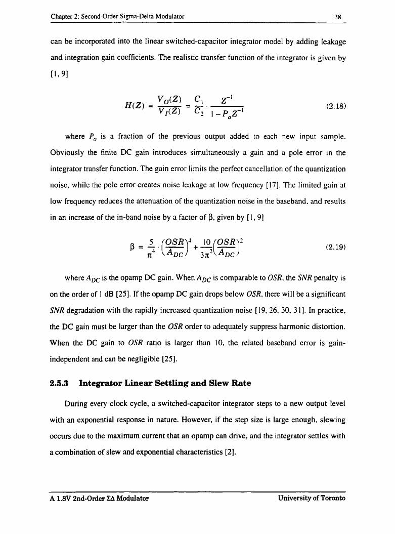
Chapter 2: Second-Order Sigma-Delta Modulator 38
can be incorporated into the linear switched-capacitor integrator mode1 by adding leakage
and integration gain coefficients. The realistic transfer function of the integrator is given by
[L 91
where Po is a fraction of the previous output added to erich new input sample.
Obviously the finite DC gain introduces simultaneously a gain and a pole error in the
integrator transfer function. The gain error limits the perfect cancellation of the quantization
noise, while the pole error creates noise leakage at low frequency [17]. The limited gain at
low frequency reduces the attenuation of the quantization noise in the baseband. and results
in an increase of the in-band noise by a factor of P. given by [ l , 91
where ADc is the opamp DC gain. When ADc is comparable to OSR. the SNR penalty is
on the order of 1 dB [25]. If the opamp DC gain drops below OSR. there wil l be a significant
SNR degradation with the npidly increased quantization noise [19.26. 30. 3 11. In practice.
the DC gain must be larger than the OSR order to adequately suppress harmonic distonion.
When the DC gain to OSR ratio is larger than 10. the related baseband error is gain-
independent and can be negligible [25].
2.5.3 Integrator Linear Settling and Slew Rate
During every clock cycle, a switched-capacitor integrator steps to a new output level
with an exponential response in nature. However, if the step size is large enough, slewing
occurs due to the maximum current that an opamp can drive, and the integrator settles with
a combination of slew and exponential characteristics [2].
A 1.8V 2nd-Order Lî Modulator University of Toronto
Chapter 2: Second-Order Sigma-De1 ta Modulator 39
Linear settling and slew rate specify the small-signal and large-signal speed
performance of an integrator respectively. In a ZA modulator. a linear settling error results
in an integrator gain error, and a limited slew rate results in harmonic distonion. which
directly degrades the large signal performance of a modulator [24, 30, 321.
Although an integrator needs a sufficient bandwidth for the signal to settle within a half
clock period. sigma-delta modulators can achieve high resolution performance even if the
integrators do not settle to the full resolution of the converter, as long as the settling process
is linear and the settling is not slew-rate limited [ l , 181. In a switched-capacitor integrator,
the settling time constant is a function of switches' on-resistance and the amplifier's load
which is equal to the integration capacitor in series with the parallel combination of the
sampling capacitor and the input transistors' capacitance. Thus. the input transistor size that
minimires the settling time constant depends on the sampling capacitor size [18].
The slew rate is also a function of the amplifier's load capacitance. Sufficient slew rate
can make the degradation of SNR negligible [2]. For a second-order EA modulator. Boser's
simulation [Il shows that the minimum amplifier's slew-rate must be 3A/Ts, where A is the
input full scale. and Ts is the sampling dock period.
Increasing slew rate and reducing settling time can be realized by using smaller
capacitances. However. the reduction in capacitor size is lirnited not only by kT/C noise, but
also practically by matching considerations as well as the cornbination of parasitic
capacitance which becomes more severe particularly at the amplifier's input.
2.5.4 Integrator Unity Gain Frequency and Phase Margin
In a typical sampled-data analog integrator, the unity gain frequency of the opamp mi
be at l e s t an order of magnitude greater than the oversampling rate [ I l . However, as
indicated in section 2.5.3, a lower unity gain frequency with a correspondingly inaccurate
settling will not impair the XA modulator performance if the settling process is linear. For an
- - - -
A 1.W 2nd-Order Eî Modulator University of Toronto
Chapter 2: Second-Order Sigma-Delta Moduiator 40
ideal integrator with a single dominant pole exponential impulse response, the response
time-constant r can be as large as the sampling period Ts [ I l . A value of T that is larger than
Ts will make the ZA modulator unstable.
In practice, however, because the settling process usually includes a signal-dependent
slewing component. and is influenced by non-dominant poles and the dependence of the
pole locations on the amplifier operating point, as well as finite switch resistances in the
switched-capacitor network [ X I , the integrator cannot operate with an exponential impulse
response. Also considering non-overlapping clocks with duty cycle slightly less than a half
clock period, the unity gain frequency must be at least twice the sampling rate [ I I . As a
general rule of thumb, the unity gain frequency should be around 5 times the sampling clock
frequency [7, 201, with a phase margin greater than 70 degrees to provide a smooth settling
characteristic 11, 7, 331.
2.5.5 Integrator Output Swing and Offset
An operational amplifier's output swing defines the maximum signal handling
capability and is directly related to the modulator input level. Maximizing the output swing
will increase the maximum dynamic range. at the same time, minimizing the required
sampling capacitance and power dissipation as described in section 2.4.3.
The output swing, ultirnately limited by the power supply voltage, is even more critical
in a low-voltage design. In practice, the output swing is lower than the supply voltage
because the output devices rnust operate in active region. To maximize the output swing, a
cornmon source output configuration must be used and a switched-capacitor common-mode
feedback circuit must be applied when using a fully-differential amplifier configuration [7].
In a second-order EA modulator. offset is only a minor concern as long as the
quantization is uniform [Il. The offset at the input to the first integrator is the only
significant contributor because offsets in the second integrator and the comparator are
A 1.8V 2nd-Order Cd Modulator University of Toronto

Chapter 2: Second-Order Sigma-Delta Modulator 4 1
suppressed by the large low-frequency gain of the integrators. In practice, to avoid large
reduction in the effective signal range, offsets should not be excessive.
2.6 Comparator-Latch Design Considerations
In the forward path of a ZA modulator, the 1-bit quantizer can be realized by a track-
and-latch comparator, which consists of a regenerative latch and a preamplify stage which
helps to increase resolution and reduce clock kickback effects [?9. 371. Kickback denotes
the charge transfer either into or out off the comparator inputs when the track-and-latch
stage goes from the track mode to the latch mode. The charge transfer is caused by the
charge needed to tum on the transistors in the positive-feedback circuitry and by the charge
that must be removed to tum off the transistors in the tracking circuitry. Without a
preamplifier, this kickback wili affect the driving circuitry and cause large glitches,
especially when the two inputs are not perfectly matched.
The main parameters of the comparator-latc h design to consider are speed, input offset.
input-referred noise. and hysteresis.
The cornparison speed rnust be higli enough to meet the desired sampling rate.
Minimum channel length must be used for al1 transistors in a comparator-latch. The gain of
the preamplify stage should not be too large to limit the cornparison speed [7].
The offset and input-referred noise at the comparator input can be suppressed by the
feedback loop of the ZA modulator [33, 34). Using PMOS transistors with large size in
preamplify stage also resuits in smaller flicker noise contribution [36].
The comparator hysteresis is very important for the modulator operation [17]. Defined
as the minimum overdrive required to change the output. it cm be modeled as an additive
white noise at the input of the comparator [ l , 28, 331, and c m be shaped out-of-band in the
same way as the quantization noise by the feedback loop [28, 341. When the hysteresis is
- - -
A 1.8V 2nd-Order &î Modulator University of Toronto
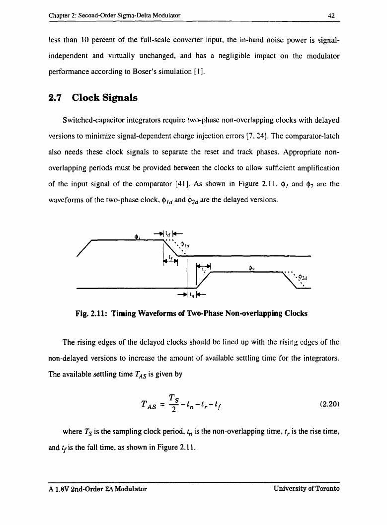
Chapter 2: Second-Order Sigma-Del ta Modulator 42
less than 10 percent of the full-scale converter input, the in-band noise power is signal-
independent and virtually unchanged, and has a negligible impact on the rnodulator
performance according to Boser's simulation [ 11.
2.7 Clock Signals
S wi tched-capacitor integrators require two-phase non-overlapping clocks w ith delayed
versions to minimize signal-dependent charge injection errors [7.?4]. The cornparator-latch
also needs these clock signals to separate the reset and track phases. Appropriate non-
overlapping periods must be provided between the clocks to allow sufficient amplification
of the input signal of the comparator [41]. As shown in Figure 2.1 1 . 41, and Qz are the
wavefoms of the two-phase clock. Qld and gZd are the delayed versions.
Fig. 2.1 1 : Timing Waveforms of Two-Phase Nonsverlapping Clocks
The nsing edges of the delayed clocks should be lined up with the rising edges of the
non-delayed versions to increase the amount of available settling time for the integrators.
The available settling tirne TAS is given by
where Ts is the sampling dock penod, t, is the non-overlapping time, r, is the rise time,
and 'fis the fail urne, as shown in Figure 2.1 1.
--- - - --- -
A 1.8V 2nd-Order ZA Modulator University of Toronto
Chapter 2: Second-Order Sigma-Deita Modulator 43
This chapter provides an overview of the theory and design principles of a second-order
sigma-delta modulator. The theory of oversampling and noise-shaping were introduced, and
demonstrated by the system-level simulation. The main considerations and trade-offs of a
modulator design were discussed in detail, as well as the required specifications of the
integrator that prirnarily determine the modulator's performance. The design considerations
of the comparator-latch and the driving dock signals were also discussed. The transistor-
level design of a modulator impiementation, which will be provided in Chapter 3. is based
on the criteria descnbed in this chapter.
- - - - - - . - - - - - -
A 1.8V 2nd-Order ZA Modulator University of Toronto
Chapter 2: Second-Order Sigma-Delta Modulator 44
References
B. Boser and B. Wooley, 'The Design of Sigma-Delta Modulator Analog-to-Digital Converters," IEEE kiirnal of Solid-Stnte Circuits. Vol. 23, pp. 1298- 1308, 1988.
K. C. H. Chao, S. Nadeern, W. L. Lee. C. G. Sodini, "A High Order Topology for Inter- polative Modulators for Oversampling A D Converters", IEEE Transactions on Cir- cuits and Systfrns, Vol. 37. pp. 309-3 18, 1990.
A. Marques, V. Peluso, M. S. J. Steyaert. and W. M. Sansen, "Optimal Parameters for Sigma-Delta Modulator Topologies", IEEE Transactions on Circuits and Systems, Vol. 45, pp. 1232-1241, 1998.
P. M. Aziz, H. V. Sorensen, and J. V. D. Spiegel. 'An Overview of Sigma-Delta Modu- lators", IEEE Signal Processing Magazine. Vol. 13. pp. 6 1-84. January, 1996.
R. W. Stewart, "An Overview of Sigma-Delta ADCs and DAC Devices". IEE Coilo- yriirirn on Oversampling and Sigmci-Delta Strntegies fur DSP. pp. 1/ 1 - 1/9, 1995.
J. W. Fattaruso. S. Kinaki. M. de Wit, and G. Warwar. "Self-Calibration Techniques for a Second-Order Mul tibit Sigma-Del ta Modulator," IEEE Journal of Solid-State Cir- cuits, Vol. 28. ~1216-1223. 1993.
K. Martin and D. Johns, Analog lntegrnted Circuit Design. John Wiley & Sons, Inc., Toronto, Canada. 1997.
K. Khoo. Progrnnimcrble High-Dvnnmic Range Sigma-Delta A/D Converters for Mdti- standard F~iliy-lntegrated RF Receivrrs. M . S . Thesis, University of California at Ber- keley, 1999.
S. J. Ma, A Low-Power Low- Voltage Second-Order Sigma-Delta Modhto,: M .A.Sc. Thesis, University of Toronto. 1998.
[IO] G. M. Yin, F. Op't Eynde, and W. Sansen. "A High Speed CMOS Comparator with 8-b Resoliition," IEEE journal of Soiid-State Circuits, Vol. 27, pp. 208-2 1 1 , 1992.
[ I l ] M. Hauser, "Principles of Oversampling N D Conversion:' J. Audio Eng. Soc., Vol. 39, pp. 3-26, 1996.
[12] E. Chan, and M. Ortiz, "Low Power Digital Oversampling Sigma-Delta Dernodulator for Audio Applications", EECS 241 Final Report, University of California, Berkeley, 1996.
1131 R. Norswonhy, 1. G. Post, and H. S. Fetterman, "A 14-bit IO-kHz Sigma-Delta A/D Converter: Modeling, Design, and Performance Evaluaiion," lEEE Journal of Solid- Stute Circuits, Vol. 24, pp. 256-265. 1989.
[14] V. Peluso, M. S. J. Steyaert, and W. Sansen. "A 1.5V lOOuW Sigma-Delta Modulator with 12-b Dynamic Range Using the Switched-Opamp Technique, IEEE Journal of Solid-State Circuits. Vol. 23, pp. 943-952, 1997.
- - - - - - - - -
A 1.8V 2nd-Order Zi Modulator University of Toronto
Chapter 2: Second-Order Sigma-Delta ModuIator 45
[15] J. C. Candy, G. C. Temes, "Ovenampling Methods for Data Conversion", IEEE Pacifzc Conference on Comrnrtnicntions, Comprrters and Signal pracessing, pp. 498-502, 199 1.
[16] R. A. Gott, "High-Resolution A/D Converters Provide A Sure Start Out of the Gate", Cornputer Design, pp. 92-93, November, 1998.
[17]A. M. Marques, V. Peluso. M. S. J. Steyaert. W. Sansen, "A 15-b Resolution 2-MHz Nyquist Rate Sigma-Delta ADC in a 1-um CMOS Technology", IEEE Jorrmnl of Solid-State Circuits, Vol. 33. pp. 1065- 1075. 1998.
[18] S. Rabii, and B. A. Wooley, "A 1.8V Digital-Audio Sigma-Delta Modulator in 0.8um CMOS," IEEE Journal of Solid-State Circuits. Vol. 32. pp. 783-795, 1997.
(191 A. R. Feldman, B. E. Boser, and P. R. Gray, "A 13-Bit 1.4-MSls Sigma-Delta Modula- tor for RF Baseband Channel Applications", IEEE Journal of Solid-Stnte Circuits, Vol. 33, pp. 1462-1469, 1998.
[?O] E. I. van der Zwan. and E. C. Dijkmans, "A 0.2mW CMOS Sigma-Delta Modulator for Speech Coding with 80dB Dynamic Range," IEEE International Solid-State Circliirs Conferericr. Digest o f Technical Papers. pp. 232-232, 1996.
[21] V. Peluso, A. Marques, M. Steyaert, W. Sansen, "Optimal Parameters for Single Loop Sigma-Delta Modulators", IEEE Proceeclings of International Symposirrrn on Circuits and Systerns. Vol. 1, pp . 57-60. 1997.
[22] S. Rabii, and B. A. Wooley, "A 1.8V 5.4mW. Digital-Audio Sigma-Delta Modulator in 1.3um CMOS," IEEE International Solid-Sture Circuits Conference, Digest of Techni- cal Papers, pp. 228-229, 1996.
[23]A. S. Sedra, K. C. Smith, Microelectronic Circuits, CBS College Publishing, New York, U.S.A., 1987.
[24] A. R. Feldman, Higli-Speed Law- Power Sigma-Delta Mudulutors for RF bïiseband Channel Applications, Ph.D. Thesis, University of Cali fomia at Berkeley, 1997.
[25] A. K. Ong, and B. A. Wooley, "A Two-Path Bandpass Sigma-Delta Modulator for Dig- ital IF Extraction at 20 MHz", IEEE Joumal of Solid-State Circuits, Vol. 32, pp. 1920- 1933, 1997.
[26] S. Au, and B. H. Leung, "A 1.95V 0.34mW 12-b Sigma-Delta Modulator Stabilized by Local feedback Loops", IEEE Joumal of Solid-State Circiiits, Vol. 32, pp. 32 1-327, 1997.
[27] 0. Nys, and R. K. Henderson, "A 19-Bit Low-Power Multibit Sigma-Delta ADC Based on Data Weighted Averaging", IEEE Joumal of Solid-State Circuits, Vol. 32, pp. 933- 942, 1997.
1281 S. Bazarjani, and W. M. Snelgrove, "A 160MHz Fourth-Order Double-Sampled SC Bandpass Sigma-Delta Modulator", IEEE Joiirnal of Soiid-State Circuits, Vol. 45, pp. 547-555, 1998.
. . -- - - -- - --p. -- - -
A 1.8V 2nd-Order ZA Modulator University of Toronto
Chapter 2: Second-Order Sigma-Delta Modulator 46
[29]T. B. Cho, D. W. Cline, C. S. G. Conroy, and P. R. Gray, "Design Considerritions for High-Speed, Low-Powei; Law- Voltage CMOS Anolog-to-Digital Converters", http://kabuki.eecs.berkeley.edu/, University of California at Berkeley, 1994.
[30]E. T. King, A. Eshraghi, 1. Galton. and T. S. Fiez, "A Nyquist-Rate Delta-Sigma M D Converter", IEEE Jo~irnal of Soiid-State Circiiits, Vol. 33, pp. 45-52, 1998.
[3 11 G. Fischer, and A. S. Davis, "Alternative Topologies for Sigma-Delta Modulators - A Comparative S tudy", IEEE Trans. on Circuits and Systerns, Vol. 44, pp. 789-797, 1997.
[32] J. C. Candy. G. C. Ternes, Oversnmpling Delta-Sigma Data Converters, EEE Press, New York, U.S.A.. 1992.
[33] S. A. Jantzi, K. W. Martin. and A. S. Sedra. "A Quadrature bandpass Sigma-Delta Modulation for Digital Radio," IEEE Internatioricil Solid-State Circuits Confrrencr, Digest of Technical Papers, pp. 226-227, 1997.
[34] S. A. Jantzi, K. W. Martin. and A. S. Sedra. "Quadrature bandpass Sigma-Delta Modu- lation for Digital Radio," lEEE Jo~irnul of Solid-Srrire Circuits, Vol. 32, pp. 1935- 1948, 1997.
[35] L. A. Williams, and B. Wooley, "A Third-Order Sigma-Delta Modulator with Extended Dynamic Range". IEEE Journal of Solid-Stare Circriifs, Vol. 29, pp. 193-202. 1994.
[36] F. Chen, and B. Leung, "A 0.25-mW Low-Pass Passive Sigma-Delta Modulator with Built-in Mixer for a IO-MHz IF hput", lEEE Joiinml ofSolid-Stare Circuits, Vol. 32. pp. 774-78 1, 1997.
[37] W. Gao, and W. M. Snelgrove, "A 950MHz IF Second-Order Integrated LC Bandpass Delta-Sigma Modulator'*, IEEE J. of Solid-Stote Circiiits, Vol. 33. pp. 723-732, 1998.
[38]S. H. Lewis. H. S. Fetterman, G. F. Gross, Jr. R. Ramachandran. and T. R. Viswanathan, "A IO-b 20-Msamplels Analog-to-Digital Converter", IEEE Jorimaf of Solid-Stote Circriits, Vol. 27, pp. 3 5 1 -358, 1 992.
[39] M. W. Hauser, "Technology Scaling and Performance Limitations in Delta-Sigma Ana- log-rligital Converters," IEEE International Symposium on Circriits and Systems, Vol. 29, pp. Vol. 1,356-359. 1990.
[40] 1. Crols, and M. Steyaert. "Sw itched-Opamp: An Approach to Realize Full CMOS Switched-Capacitor Circuits at Very Low Power Supply Voltages", IEEE Journal of Solid-State Circuits, Vol. 29, pp. 936-942, 1994.
[41] D. Senderowicz, G. Nicollini, S. Pemici, P. Confalonieri, and C. Dallavalle, "Low Volt- age Double Sampled Sigma-Delta Converters", IEEE International Solid-State Circuits Conference, Digest of Technical Papers, pp. 2 10-2 1 1, 1997.
[42] J. Grilo, E. MacRobbie, R. Halim and G. Ternes, "A 1.8V 94dB Dynarnic Range Sigma-Delta Modulator for Voice Applications,*' IEEE Inremational Solid-State Cir- cuits Conference, Digest of Technical Papers, pp. 230-23 1, 1996.
A 1.8V 2nd-Order XA Modulator University of Toronto

Chapter 3: Modulator Design and Impiementation 47
CHAPTER 3
Modulator Design and Implementation
The second-order ZA modulator, illustrated in Figure 3.1. was designed and
implemented using a 3.3 V, 0.35prn CMOS technology. The building blocks include the
bias circuit, the operational amplifier, the comparator-latch,
building blocks are discussed in the following paragraphs.
and the clock generator. These
- - - - - - - - 1
Fig. 3.1: Btock Diagram of the Second-Order Sigma-Delta Modulator
A 1.8V 2nd-Order Z î Modulator Universi@ of Toronto
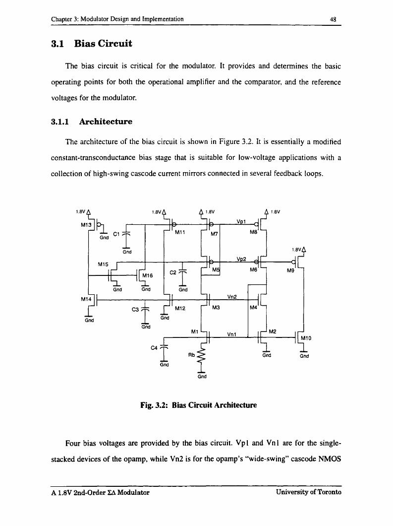
Chapter 3: Modulator Design and Implementation 48
3.1 Bias Circuit
The bias circuit is critical for the modulator. It provides and determines the basic
operating points for both the operational amplifier and the comparator, and the reference
voltages for the modulator.
3 1 1 Architecture
The architecture of the bias circuit is shown in Figure 3.2. It is esscntially a modified
constant-transconductance bias stage that is suitable for low-voltage applications with a
collection of high-swing cascode cuvent rnirrors connected in several feedback loops.
A Gnd
Fig. 3.2: Bias Circuit Architecture
Four bias voltages are provided by the bias circuit. Vpl and Vnl are for the single-
stacked devices of the opamp, while Vn2 is for the opamp's "wide-swing" cascode NMOS
A 1.8V 2nd-Order ZA Modulator University of Toronto
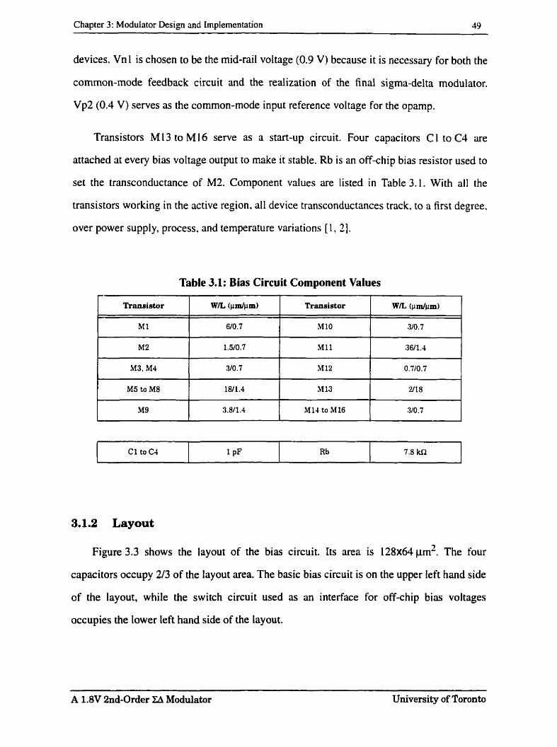
Chapter 3: Modulritor Design and Irnplementation 49
devices. Vn 1 is chosen to be the mid-rail voltage (0.9 V) because it is necessary for both the
common-mode feedback circuit and the realization of the final sigma-delta modulator.
Vp2 (0.4 V) serves as the common-mode input reference voltage for the oparnp.
Transistors M 13 to M 16 serve as a start-up circuit. Four capacitors C l to C4 are
attached at every bias voltage output to make it stable. Rb is an off-chip bias resistor used to
set the transconductance of M2. Component values are listed in Table 3.1. With al1 the
transistors working in the active region. al1 device transconductances track. to a first degree.
over power supply, process, and temperature variations [1. 2).
Table 3.1 : Bias Circuit Component Values
3.1.2 Layout
Figure 3.3 shows the layout of the bias circuit. Its area is 128x64 pn2. The four
capacitors occupy 2/3 of the layout area. The basic bias circuit is on the upper left hand side
of the layout, while the switch circuit used as an interface for off-chip bias voltages
occupies the lower left hand side of the Iayout.
WIL (pm/pm)
3/0. 7
A U V 2nd-Order ZA Modulator University of Toronto
Transistor
rMl0
Transistor
Ml
W L (pmlpm)
6/0. 7
Chapter 3: Modulator Design and Implementation 50
I Capacitors I
Fig. 3.3: Layout of Bias Circuit
3.1.3 Simulation Results
Table 3.2 lists the four output voltages and the power dissipation from the post-layout
simulation of the bias circuit.
Table 3.2: Post-layout Simulation Results of Bias Circuit
I Parame ter Value
3.2 Operational Amplifier
- Vnl
Vn2
VP 1
V P ~
Power Dissipation
In a XA modulator design, the operational amplifier is the most important component
that determines the accuracy of the discrete-time integrator, thus determining the
performance of the final ZA rnodulator.
- .-
0.899 V
1.239 V
0.865 V
0.398 V
173.7 p W
- - - -- -
A 1 -8V 2nd-Order EA Modulatoi University of Toronto
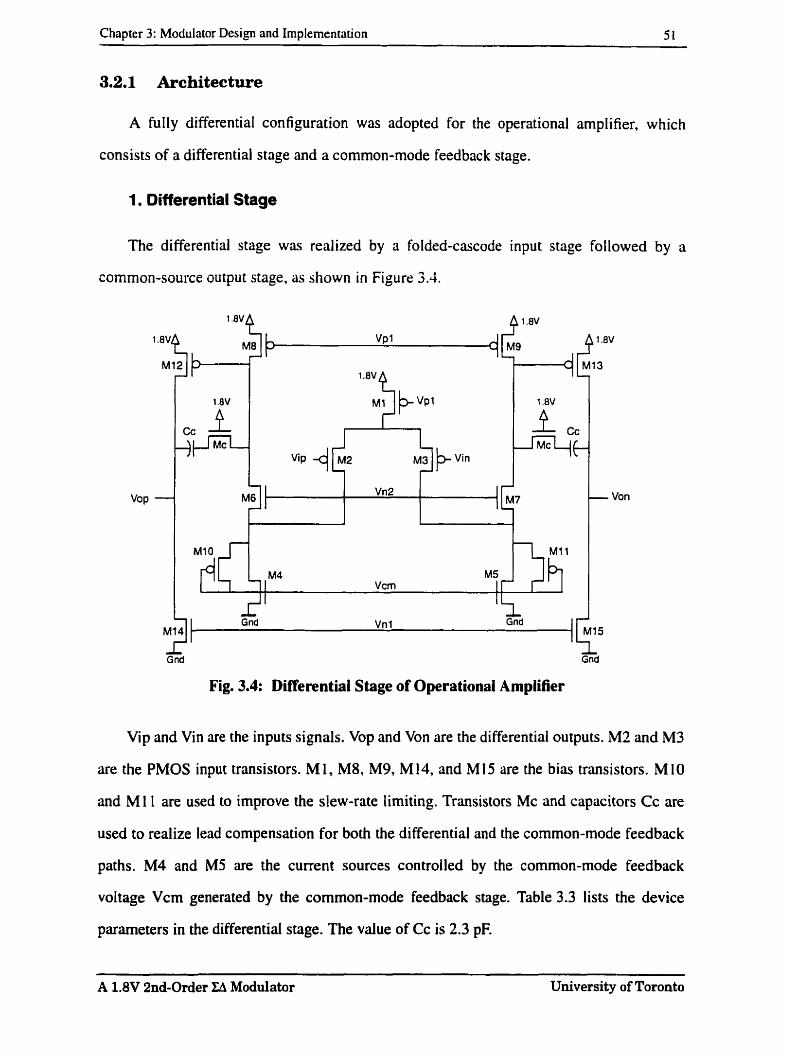
Chapter 3: Modulator Design and Implementation 5i
3.2.1 Architecture
A fully differential configuration was adopted for the operational amplifier, which
consists of a differential stage and a common-mode feedback stage.
1. Differential Stage
The differential stage was realized by a folded-cascode input stage followed by a
common-source output stage, as shown in Figure 3.4.
- Von
G nd Gnd
Fig. 3.4: Differential Stage of Operational Amplifier
Vip and Vin are the inputs signals. Vop and Von are the differential outputs. M2 and M3
are the PMOS input transistors. M 1, M8. Mg, M 14, and M 15 are the bias transistors. M 10
and M l I are used to improve the slew-rate limiting. Transistors Mc and capacitors Cc are
used to realize l e d compensation for both the differential and the comrnon-mode feedback
paths. M4 and M5 are the current sources controlled by the common-mode feedback
voltage Vcm generated by the common-mode feedback stage. Table 3.3 lists the device
parameters in the differential stage. The value of Cc is 2.3 pF.
-- - -
A 1.8V 2nd-Order ZA Modulator University of Toronto
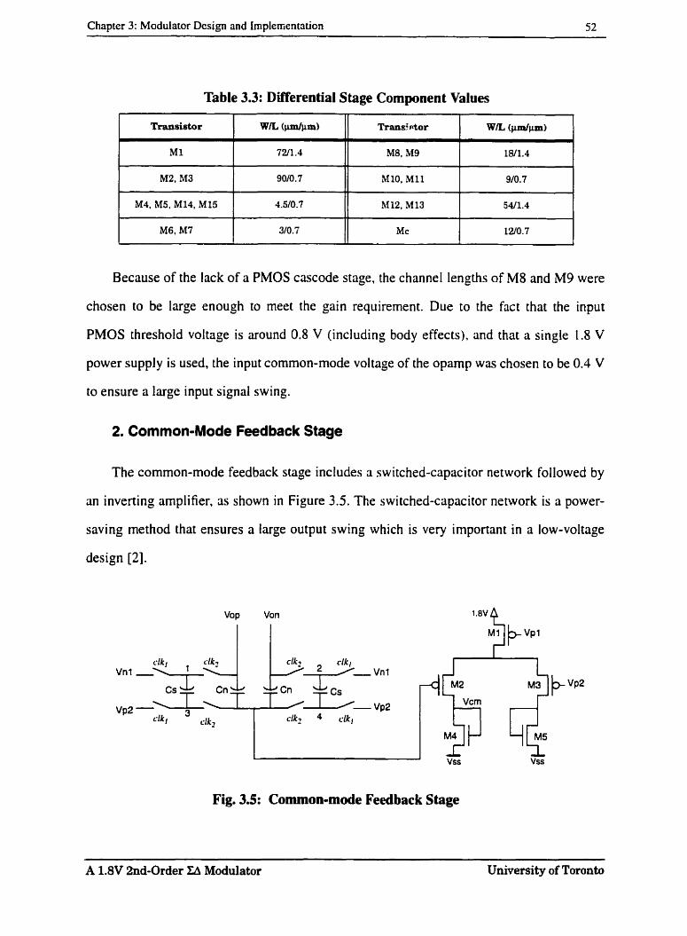
Chapter 3: Modulator Design and Irnplenientiition 52
Table 3.3: Differential Stage Component Values
Because of the lack of a PMOS cascode stage, the channel lengths of M8 and M9 were
chosen to be large enough to meet the gain requirement. Due to the fact that the input
PMOS threshoid voltage is around 0.8 V (including body effects), and that a single 1.8 V
power supply is used. the input common-mode voltage of the opamp was chosen to be 0.4 V
to ensure a large input signal swing.
2. Common-Mode Feedback Stage
The common-mode feedback stage includes a switched-capacitor network followed by
an inverting amplifier, as shown in Figure 3.5. The switched-capacitor network is a power-
saving method that ensures a large output swing which is very important in a low-voltage
design [2].
Vop Von
Vcm vp2 -
slk clk2 clk2 4 d k l
vss vss
Fig. 3.5: Common-mode Feedback Stage
A 1.8V 2nd-Order ZA Modulator UniversiS. of Toronto

Chapter 3: Modulritor Design and Im plementation 53
Vcm is the common-mode feedback voltage generated by this common-mode feedback
stage. It is applied to the gates of transistors M4 and M5 in Figure 3.4 to ensure a large
cornmon-mode loop gain. The differentiai outputs Vop and Von are averaged through the
non-switched capacitors labelled Cn, and the DC levels are maintained through the
switched capacitors labeiled Cs [1, 2, 81.
In Figure 3.5, the switches connected to nodes 1 and 2 are realized by CMOS
transmission gates to accommodate a wider output swing. The switches connected to nodes
3 and 4 can only be implemented using an NMOS pass transistor because of the low
reference voltages (Vp2 = 0 .W) . The on-resistance of each switch must be as small as
possible. To realize a high speed performance. the transistor channel iength of al1 the
switches is chosen to be minimum.
The capacitors Cn and Cs affect the slew rate and the phase margin of the opamp.
Normally Cs is chosen to be srnaller than Cn [ 11. Table 3 .J lists the component parameters
in the common-mode feedback stage.
Table 3.4: Common-mode Feedback Stage Component Values
3.2.2 Layout
The layout of the operational amplifier is shown in Figure 3.6. Its area is 420x1 30 pm2.
Most of the area is occupied by the capacitors. Three more binary-weighted capacitors
ranging from 0.5 pF to 2 pF were generated and connected paralle1 to the compensation
capacitors Cc by switches. So the compensation capacitance can be changed to cornpensate
for the possible effects of processing variations when the chip is being tested.
Transistor
Ml
M2, M3
M4, M5
A 1.8V 2nd-Order CLI Modulator University of Toronto
Value
500 fF
200 fF
W/L (umfprn)
36/1.4
30/0.7
1.5/0.7
Capacitor
Cn
Cs
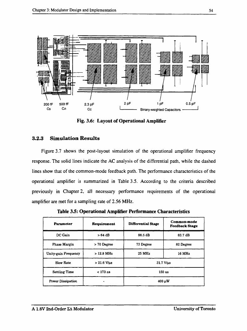
Chapter 3: Modulator Design and Implementation 54
Fig. 3.6: Layout of Operational Amplifier
3.2.3 Simulation Results
Figure 3.7 shows the post-layout simulation of the operational amplifier frequency
response. The solid lines indicate the AC analysis of the differential path. while the dashed
lines show that of the common-mode feedback path. The performance characteristics of the
operational amplifier is sumrnarized in Table 3.5. According to the criteria described
previously in Chapter 2. al1 necessary performance requirernents of the operationai
amplifier are met for a sampling rate of 2.56 MHz.
Table 3.5: Operational Amplüier Performance Characteristics
Parameter
DC Gain
Phase Margin
Unity-gain Frequency
1 Power Dissipation [ 1
Requisement
Slew Rate
Settliag Time
A 1.8V 2nd-Order Eî Modulator University of Toronto
> 64 dB
> 70 Degree
> 12.8 MHz
Differential Stage
> 21.6 V/ps
< 173 ns
Common-mode Feedbsek Stsge
88.5 dB
73 Degree
25 MHz
31.7 V l p
150 ns
83.7 dB
82 Degree
16 MHz

Chapter 3: Modulator Design and Implernentation 55
- - --- - CIE-P O C 0 e o a: - V O B C V O P V O N - :-
- - C M P LICO
s a . O r - v o e r V C M F O U T - - - .(a . O 1 - -
- 2 0 0
- - o r
z q 9 L , . , , a ,
-- \ - \ Z A E - P a c o - 1 5 0 O = \ V P I V 0 P . V O N - - - -L.
- C M P A C 0 \-----
- 1 0 0 O 1 - - - - - - V P C V C M F O U T - - - - - - 1 - -
5 0 0 r xl - - - -
-
- - 5 0 O r
- - i o a o r
t , 1 , , , , , , 1 , 1 1 , ,,,, 1 , 1 1 1 1 1 1 1 1 , 1 1 1 , 1 1 1 1 1 1 1 1 1 * 1
I O K 1 O O K 1 0 0 oic 1 o x I O o x 1 0 0 O H E R T Z C L O G l l a 0 O X
Fig. 3.7: Post-Layout Simulation of Operational Amplifier
The cornrnon-mode feedback stage is well compensated with a phase margin of
82 degrees. This is necessary otherwise the injection of common-mode sipnals can cause
the circuit to ring and become unstable. It also has a speed-performance comparable to the
unity-gain frequency of the differential stage, otherwise the noise on the power supplies
may be significantly mplified such that the output signal becomes clipped [ I l . In this
design, since the common-mode path actually shares the same dominant pole and the
second pole with the differential path, as illustrated in Figure 3.7, the frequency response of
both paths are comparable to each other.
3.3 Comparator-Latch
The cornparator-latch determines the output of the second integrator and generates
either a "one" or a "zero" digital signal within half a clock penod. These digital signals are
A 1.8V 2nd-Order U Modulator UniversiS. of Toronto
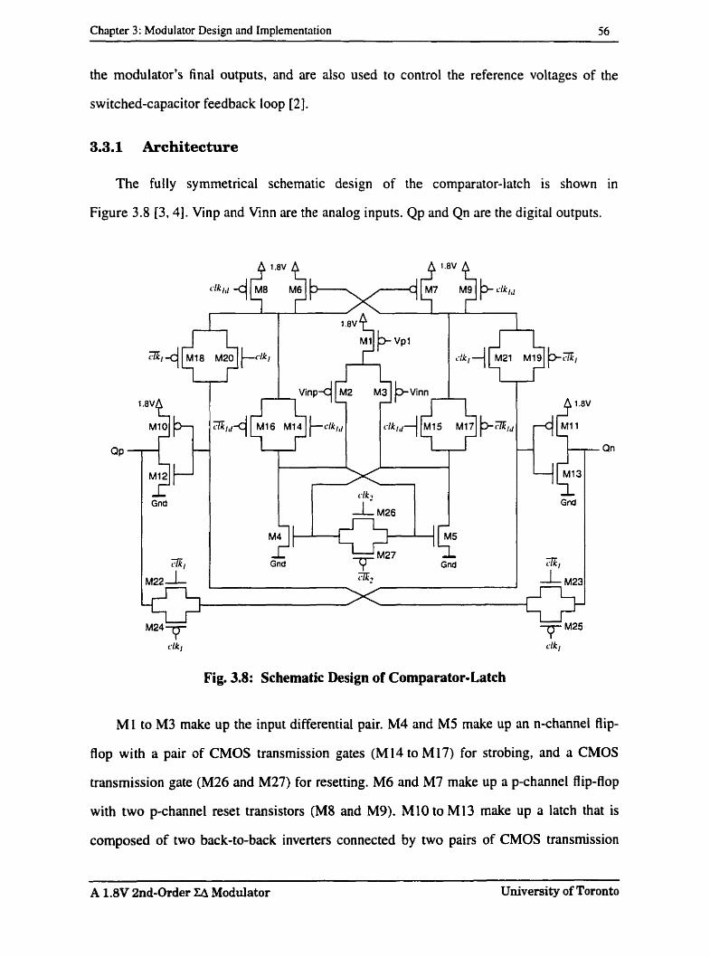
Chapter 3: Modulator Design and Implementation 56
the modulator's final outputs. and are also used to control the reference voltages of the
switched-capacitor feedback loop [2].
3.3.1 Architecture
The fully symmetrical schematic design of the comparator-latch is shown in
Figure 3.8 [3.4]. Vinp and Vinn are the analog inputs. Qp and Qn are the digital outputs.
Gnd
Fig. 3.8: Schematic Design of Comparator-Latch
M l to M3 make up the input differential pair. M4 and M5 make up an n-channel Bip-
Bop with a pair of CMOS transmission gaies (M 14 to M 17) for strobing, and a CMOS
transmission gate (M26 and M27) for resetting. M6 and M7 make up a p-channel flip-flop
with two p-channel reset transistors (M8 and M9). M l 0 to M l 3 make up a latch that is
composed of two back-to-back inverters connected by two pairs of CMOS transmission
A 1.8V 2nd-Order ZA Modulator UniversiS. of Toronto
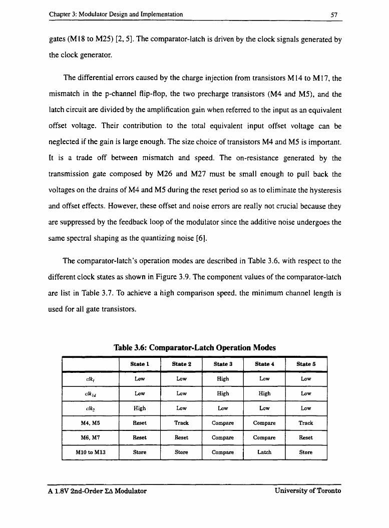
Chapter 3: Modulator Design and Implementation 57
gates (M 18 to M25) [2,5]. The comparator-latch is driven by the dock signals generated by
the dock generator.
The differential errors caused by the charge injection from transistors M 14 to M 17, the
mismatch in the p-channel flip-flop. the two precharge transistors (M4 and MS), and the
latch circuit are divided by the amplification gain when referred to the input as an equivalent
offset voltage. Their contribution to the total equivalent input offset voltage cm be
neglected if the gain is large enough. The size choice of transistors M4 and M5 is important.
It is a trade off between mismatch and speed. The on-resistance generated by the
transmission gate composed by M26 and M27 rnust be srnall enough to pull back the
voltages on the drains of M4 and M5 during the reset period so as to eliminate the hysteresis
and offset effects. However, these offset and noise errors are really not crucial because they
are suppressed by the feedback loop of the modulator since the additive noise undergoes the
same spectral shüping as the quantizing noise [ 6 ] .
The comparator-latch's operation modes are described in Table 3.6. with respect to the
different dock States as shown in Figure 3.9. The component values of the comparûtor-latch
are iist in Table 3.7. To achieve a high cornparison speed. the minimum channel length is
used for al1 gate transistors.
Table 3.6: Comparator-Latch Operation Modes
rlk,
dkld
c k
M4, M5
- --
A 1.8V 2nd-Order ZA Modulator University of Toronto
M6, M7
M l 0 to M l 3
Low
Low
High
Rese t
Reset
Store
Low
Law
Low
Track
Reset
Store
High
High
Law
Compare
Compare
Compare
Low
High
Low
Compare
Low
Law
Low
Track 1
Compare
Latch
Reset
Store
Chripter 3: Modulator Design and Irnplementation 58
Fig. 3.9: 4-Phase Clock Signals
Table 3.7: Comparator-Latch Component Values
-- - -- -
3.3.2 Layout
Figure 3.10 is the layout of the comparator-latch.
P-channel Switches and Back-to-Back
Inverters
Fig. 3.10: Comparator-Latch Layout
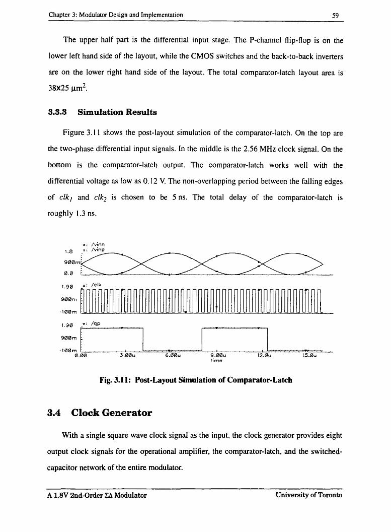
Chapter 3: ModuIator Design and Implementation 59
The upper half part is the differential input stage. The P-channel flip-flop is on the
lower left hand side of the layout. while the CMOS switches and the back-to-back inverters
are on the lower right hand side of the layout. The total comparator-latch layout area is
38x25 pm'.
3.3.3 Simulation Resdts
Figure 3.1 1 shows the post-layout simulation of the comparator-latch. On the top are
the two-phase differential input signals. In the middle is the 2.56 MHz clock signal. On the
bottom is the comparator-latch output. The comparator-latch works well with the
differential voltage as low as 0.12 V. The non-overlapping penod between the falling edges
of clk,
roughl y
1.8
and clkz is chosen to be 5 ns. The total delay of the comparator-latch is
1.3 m.
Fig. 3.11: Post-Layout Simulation of Comparator-Latch
3.4 Clock Generator
With a single square wave clock signal as the input, the clock generator provides eight
output clock signais for the operational amplifier, the comparator-latch, and the switched-
capacitor network of the entire modulator.
A 1.8V 2nd-Order Li Modulator University of Toronto
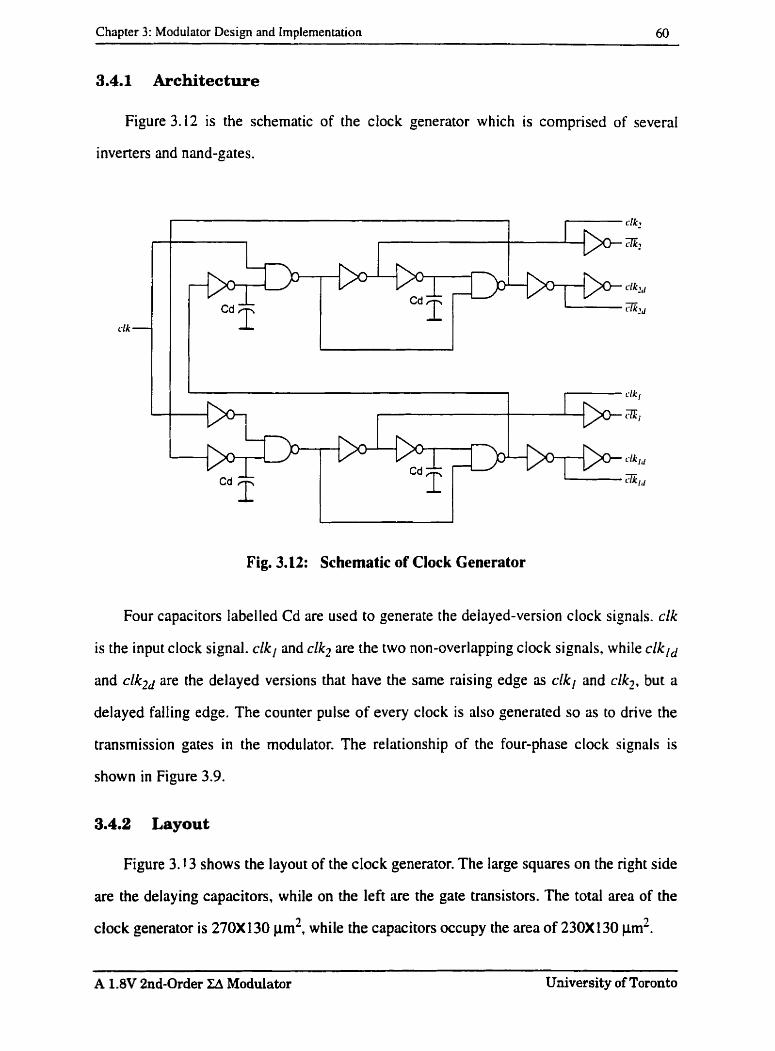
Chapter 3: ModuIator Design and Irnplemencation 60
3.4.1 Architecture
Figure 3.12 is the schematic of the clock generator which is compnsed of several
inverten and nand-gates.
d k 2
clkJd
clk -
Clk,
Fig. 3.12: Schematic of Clock Generator
Four capacitors labelled Cd are used to generate the deiayed-version clock signais. clk
is the input clock signal. cikl and clkt are the two non-overlapping dock signals, while d k I d
and clkzd are the delayed versions that have the same raising edge as clkl and c-. but a
delayed falling edge. The counter pulse of every clock is also generated so as to drive the
transmission gates in the modulator. The relationship of the four-phase clock signais is
shown in Figure 3.9.
3.4.2 Layout
Figure 3.13 shows the layout of the clock generator. The large squares on the right side
are the delaying capacitors, while on the left are the gaie transistors. The total area of the
clock gnerator is Z7OX 130 pn2, while the capacitors occupy the area of 23OX 130 ~ m ' .
A 1.8V 2nd-Order ZA Modulator Uaiversity of Toronto
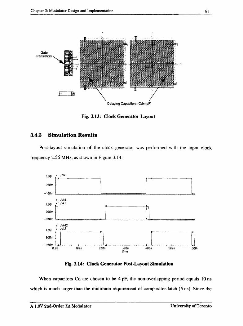
Chapter 3: Modulator Design and Implernentation 6 1
Delaying Capacitors (Cd=4pF)
Fig. 3.13: Clock Generator Layout
3.4.3 Simulation Results
Post-layout simulation of the clock generator was performed with the input clock
frequency 2.56 MHz. as shown in Figure 3.14.
Fig. 3.14: Clock Generator Post-Layout Simulation
When capacitors Cd are chosen to be 4 pF, the non-overlapping period equals 10 os
which is much larger than the minimum requirement of comparator-latch (5 ns). Since the
A 1.8V 2nd-Order ZA Modulator University of Toronto
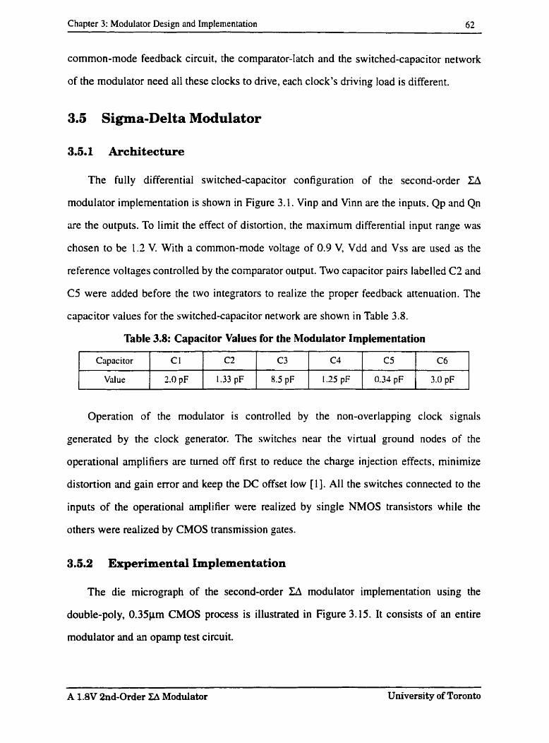
Chapter 3: Modulator Design and Implernentation 62
common-mode feedback circuit, the comparator-Iatch and the switched-capacitor network
of the modulator need al1 these clocks to drive, each clock's driving load is different.
3.5 Sigma-Delta Modulator
3.5.1 Architecture
The full y differential swi tched-capaci tor configuration of the second-order TA
modulator irnplementation is shown in Figure 3.1. Vinp and Vinn are the inputs, Qp and Qn
are the outputs. To limit the effect of distortion, the maximum differential input range was
chosen to be 1.2 V. With a cornmon-mode voltage of 0.9 V, Vdd and Vss are used as the
reference voltages controlled by the comparator output. Two capacitor pairs labelled C2 and
CS were added before the two integrators to realize the proper feedback attenuation. The
capacitor values for the switched-capacitor network are shown in Table 3.8.
Table 3.8: Capacitor Values for the Modulator Implementation
Operation of the modulator is controlled by the non-overlapping dock signais
generated by the dock generator. The switches near the vinual ground nodes of the
operational amplifiers are turned off first to reduce the charge injection effects, minimize
distortion and gain error and keep the DC offset low [ I l . A11 the switches connected to the
inputs of the operational amplifier were realized by single NMOS transistors while the
others were realized by CMOS transmission gates.
3.5.2 Experimental Implementation
The die micrograph of the second-order ZA modulator irnplernentation using the
double-poly, 0.35prn CMOS process is illustrated in Figure 3.15. It consists of an entire
rnodulator and an oparnp test circuit.
C3
1 .25 pF
Cripaci tor
Value
-- - -
A 1.8V 2nd-Order ZA Modulator University of Toronto
C2
1.33 pF
CI
2.0 pF
C3
8.5 pF
C5
0.34 pF
C6
3.0 pF
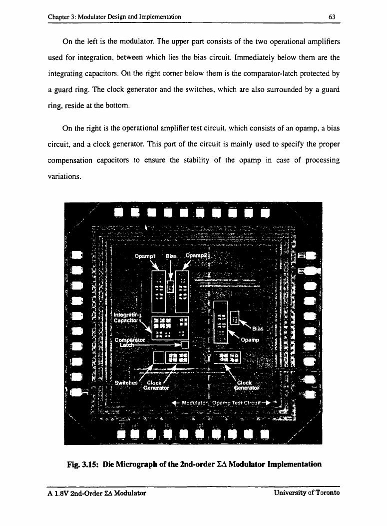
Chapter 3: Modulator Design and ImpIementation 63
On the left is the modulator. The upper part consists of the two operational amplifiers
used for integration, between which lies the bias circuit. Immediately below them are the
integrating capacitors. On the right corner below thern is the cornparator-latch protected by
a guard ring. The clock generator and the switches. which are also surrounded by a guard
ring, reside at the bottom.
On the right is the operational amplifier test circuit, which consists of an opamp, a bias
circuit, and a clock generator. This part of the circuit is mninly used to specify the proper
compensation capacitors to ensure the stability of the opamp in case of processing
variations.
Fig. 3.15: Die Micrograph of the 2nd-order ZA Modulator implementation
A 1.8V 2nd-Ordet Ch Modulator University of Toronto
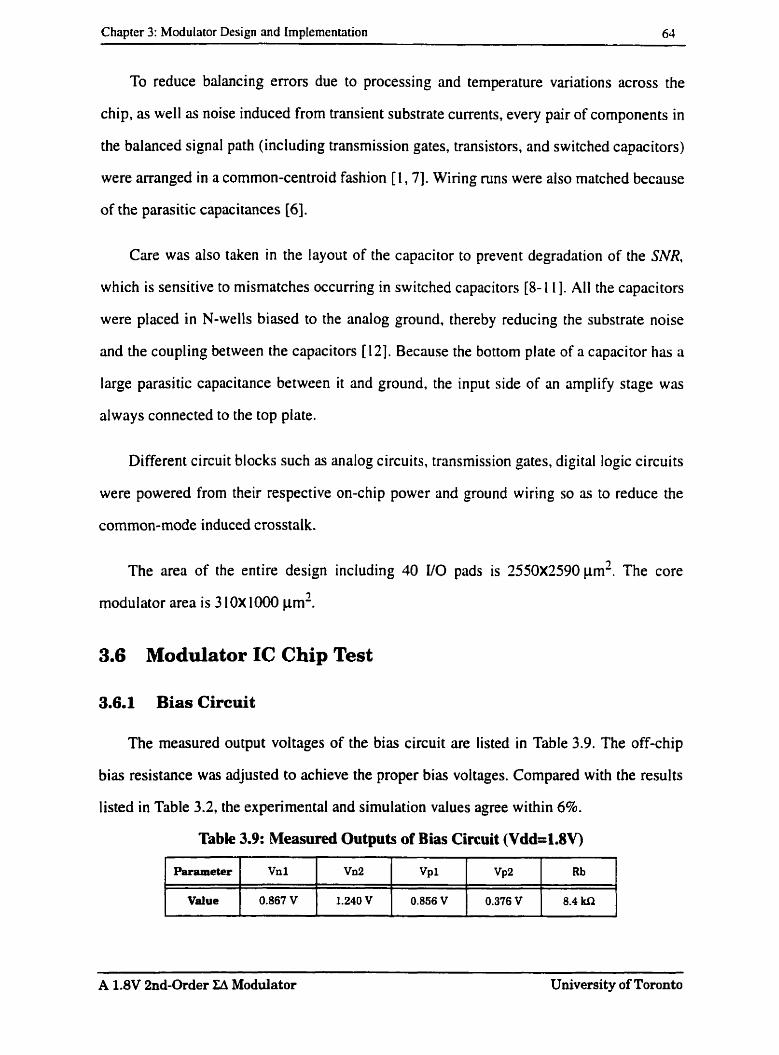
Chapter 3: Modulator Design and IrnpIementation 64
To reduce balancing errors due to processing and temperature variations across the
chip, as well as noise induced from transient substrate currents, every pair of components in
the balanced signal path (including transmission gates, transistors. and switched capacitors)
were arranged in a common-centroid fashion [ l , 71. Wiring mns were also matched because
of the parasitic capacitances [6] .
Care was also taken in the layout of the capacitor to prevent degradation of the SNR.
which is sensitive to mismatches occurring in switched capacitors [8- 1 11. All the capacitors
were placed in N-wells biased to the analog ground, thereby reducing the substrate noise
and the coupling between the capacitors [12]. Because the bottom plate of a capacitor has a
large parasitic capacitance between it and ground, the input side of an ampiify stage was
always connected to the top plate.
Different circuit blocks such as analog circuits. transmission gates, digital logic circuits
were powered from their respective on-chip power and ground wiring so as to reduce the
common-mode induced crosstalk.
The area of the entire design including 40 UO pads is 2550X259OPm7. The core
rnodulator area is 3 1 OX 1000
3.6 Modulator IC Chip Test
3.6.1 Bias Circuit
The measured output voltages of the bias circuit are listed in Table 3.9. The off-chip
bias resistance was adjusted to achieve the proper bias voltages. Compared with the results
listed in Table 3.2. the experimental and simulation values agree within 6%.
Table 3.9: Measured Outputs of Bias Circuit (Vdd=l.gV)
A 1.8V 2nd-Order ZA Modulator University of Toronto
Parameter
Value
Vnl
0.867 V
Vn2
1.240 V
Rb
8.4 kn
V P ~
0.856 V
V P ~
0.376 V
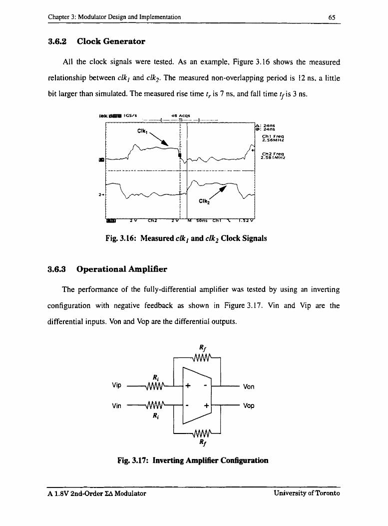
Chapter 3: Modulator Design and Implementation 65
3.6.2 Clock Generator
Al1 the dock signals were tested. As an example, Figure 3.16 shows the measured
relationship between clkl and clk2. The measured non-overiapping period is 12 m. a little
bit larger than simulated. The measured rise time r , is 7 ns, and fall time v i s 3 ns.
Fig. 3.16: Measured clkl and clkz Clock Signnls
3.6.3 Operational Amplifier
The performance of the fully-differential amplifier was tested by using an inverting
configuration with negative feedback as shown in Figure 3.17. Vin and Vip are the
differential inputs. Von and Vop are the differential outputs.
Fig. 3.17: lnverting Amplilier Contiguration
-- - - --
A 1.8V 2nd-&der ZA Moddator ~Aversity of ~ i ronto
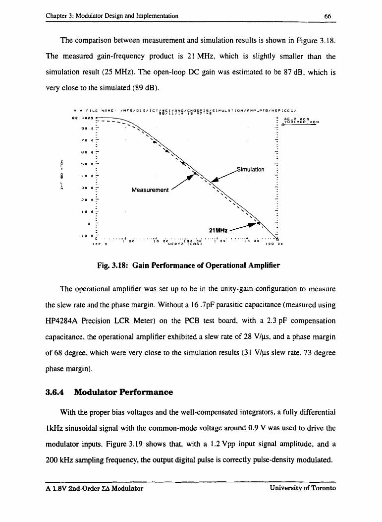
Chapter 3: Modulator Design and Implementation 66
The cornparison between measurement and simulation results is shown in Figure 3.18.
The measured gain-frequency product is 21 MHz, which is slightly smaller than the
simulation result (25 MHz). The open-loop DC gain was estimated to be 87 dB. which is
very close to the simulated (89 dB).
- C I E - P n t O V o 8 C V a P . V O N
7 0 0
6 0 O
v O 5 0 0 : L
O * O or L
N 3 0 0: Measurement 2 0 or
I O or
0 T
t O a - c . , . , , , , , I , * , , ,. 1 ai:
1 0 0 a 1 0 0 o x
Fig. 3.18: Gain Pedormance of Operational Amplifier
The operational amplifier was set up to be in the unity-gain configuration to measure
the slew rate and the phase margin. Without a 16.7pF parasitic capacitance (measured using
HP4284A Precision LCR Meter) on the PCB test board, with a 2.3 pF compensation
capacitance, the operational amplifier exhibited a slew rate of 28 V/ps, and a phase margin
of 68 degree, which were very close to the simulation results (3 1 V / p slew rate. 73 degree
phase margin).
3.6.4 Modulator Performance
With the proper bias voltages and the well-compensated inteptors. a full y differen tid
lm sinusoidal signal with the common-mode voltage around 0.9 V was used to drive the
modulator inputs. Figure 3.19 shows ihat, with a 1.2 Vpp input signal amplitude, and a
2 0 kHz sampling frequency, the output digital pulse is correctly pulse-density modulated.
A 1.8V 2nd-Order Modulator University of Toronto
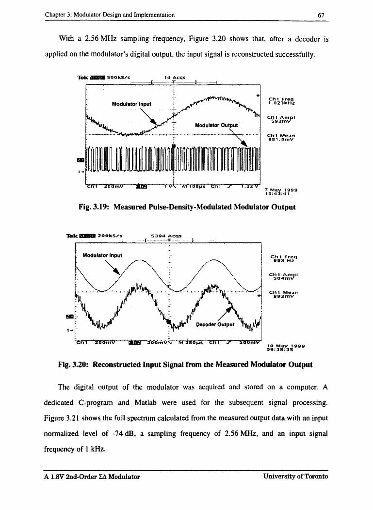
Chapter 3: Modulator Design and ImpIementation 67
With a 2.56 MHz sampling frequency, Figure 3.20 shows that. after a decoder is
applied on the modulator's digital output, the input signal is reconstructed successfully.
Tek 5 0 0 kS/s 1 4 Acqs . ---T--1------t
l. . . . ' . ' . - - - - . . . - . . . i . . . . ' ' . . . ' . " ' - - - 1
Ch1 Freq 1 - 0 2 3 k H z
Ch1 Am I 5 9 2 r n J
Ch1 Mean 891 -9mV
m 1+
Fig. 3.19: Measured Pulse-Density-Modulated Modulator Output
p s C ~ I / sbbrnv 10 May 1 9 9 9 09:38:35
Fig. 3.20: Reconstmcted Input Signal from the Measured Modulator Output
The digital output of the modulator was acquired and stored on a computer. A
dedicated C-program and Matlab were used for the subsequent signal processing.
Figure 3.2 1 shows the full spectrum calculated from the measured output data with an input
normalized level of -74 dB, a sampling frequency of 2.56 MHz, and an input signal
frequency of 1 kHz.
A 1.8V 2nd-Order 23 Modulator University of Toronto
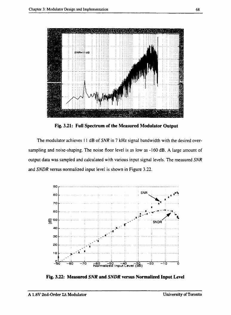
Chapcer 3: Moduiator Design and Implementation 68
Fig. 3.21: Full Spectrum of the Measured Modulator Output
The modulator achieves I I dB of SNR in 7 kHz signal bandwidth with the drsired over-
sarnpling and noise-shaping. The noise Roor level is as low as - 160 dB. A large amount of
output data was sampled and calculated with various input signal levels. The measured SNR
and SNDR versus normalized input level is shown in Figure 3.22.
Fig. 3.22: Measured SNR and SNDR versus Normalized Input Level
A 1.8V 2nd-Order ZA Modulator University of Toronto
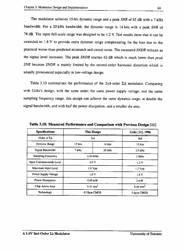
Chapter 3: Modulator Design and Irnplementation 70
This chapter has dealt with the design and implementation of a low-voltage low-power
2nd-order ZA modulator. The design and layout of ail the building biocks were presented
and discussed. Post-layout simulations and measured results showed that each block works
well with satisfactory performance. The modulator was realized wi th a fui l y-di fferential
switched-capacitor configuration and was implernented using a 0.35gm CMOS process.
Both functional and performance tests were perfomed on the modulator IC chip. Measured
results revealed that the rnodulator oversampling at 2.56 MHz has 15-bit dynamic range
with a 7 kHz bandwidth. and a 14-bit dynamic range wiih a 70 kHz bandwidth, while
dissipating 0.99 rnW of power. The die area is 0.3 1 mm2 without VO pads.
A 1.8V 2nd-Order ZA Modulator University of Toronto
Chapter 3: Modulator Design and Irnplementiition 7 1
References
K. Martin and D. Johns, Analog Integmted Circuit Design, John Wiley & Sons, Inc., Toronto, Canada, 1997.
S. Rabii, and B. A. Wooley, "A 1.8V Digital-Audio Sigma-Delta Modulator in 0.8um CMOS," IEEE Journal ofSolid-State Circuits, Vol. 32, pp. 783-795, 1997.
V. Peluso, M. S. J. Steyaert, and W. Sansen. "A 1.W lOOuW Sigma-Delta Modulator with 12-b Dynamic Tange Using the Switched-Opamp Technique, IEEE Jolournal of Solid-State Circuits, Vol. 23, pp. 943-952, 1997.
S. J. Ma, A Loiv-Power Loiv- Voltage Second-Order Sigma- Delta Modulato,: M. A.Sc. Thesis, University of Toronto, 1998.
G. M. Yin, F. Op't Eynde, and W. Sansen, "A High Speed CMOS Comparator with 8-b Resolution," IEEE Journal of Solid-Stote Circiiits. Vol. 27, pp. 108-2 1 1 , 1992.
B. Boser and B. Wooley. "The Design of Sigma-Delta Modulator Analog-to-Digital Converters," IEEE Journal of Solid-State Circuits, Vol. 23. pp. 1298- 1308, 1988.
S. R. Norsworthy, 1. G. Post, and H. S. Fetteman, "A 14-bit 80-kHz Sigma-Delta A/D Converter: Modeling, Design, and Performance Evaluation," IEEE Jortmnl of Solid- Stnte Circuits, Vol. 24, pp. 256-265, 1989.
S. A. Jantzi, K. W. Martin, and A. S. Sedra, "Quadrature bandpass Sigma-Delta Modu- lation for Digital Radio," IEEE Jotrrnal of Solid-State Circuits, Vol. 32, pp. 1935- 1948, 1997.
D. Senderowicz, G. Nicollini, S. Pernici, P. ConfaIonieri, and CI Dallavalle, "Low Volt- age Double Sampled Sigma-Delta Converten", lEEE International Solid-State Circuits Conference, Digest of Tec hnical Papers, pp. 2 10-2 1 1, 1 997.
[IO] O. Nys, and R. K. Henderson, "A 19-Bit Low-Power Multibit Sigma-Delta ADC Based on Data Weighted Averaging", IEEE Journal of Solid-Stnte Circuits. Vol. 32, pp. 933- 942, 1997.
[l III. Grilo, E. MacRobbie, R. Halim and G. Ternes, "A 1.8V 94dB Dynamic Range Sigma-Delta Modulator for Voice Applications," IEEE International Sofid-State Cir- cuits Conference, Digest of Technical Papers, pp. 230-23 1, 1996.
[12] S. Au, and B. H. Leung, "A 1.95V 0.34mW 12-b Sigma-Delta Modulator Stabilized by Local feedback Loops", IEEE Journal of Mid-Stute Circuits, Vol. 32, pp. 32 1-327, 1997.
A 1.8V 2nd-Order Eî Modulator University of Toronto
Chapter 4: Conclutions 72
CHAPTER 4
Conclusions
The second-order ZA rnodulator constitutes an efficient architecture for implementing
high-resolution A/D converters in scaled high-performance integrated circuit technology.
This thesis investigated the design and the implementation of a low-power low-voltage
second-order ZA modulator for portable communication devices using a double-poly,
0.35pm CMOS process. which is optimized for digital circuits.
The theory of oversampling and noise shaping were presented and illustrated by
system-level simulations. Detailed design considerations and analytic results have been
used to establish the design criteria for the analog circuit blocks comprising the modulator.
Specifically, the integrator linearity has a crucial influence on the performance of the
modulator. whereas the ZA modulator imposes only modest dernands on the integrator's
bandwidth, and is relatively insensitive to the offset and hysteresis in the comparator.
The fully-differential operational amplifier is the most important cornponent. which
mainly limits the performance of the M modulator's performance. The finite DC gain limits
the modulator's dynamic range, while the frequency characteristics detemines the
maximum oversampling ratio. In a low-voltage environment, the voltage swing must be
maximized to ensure a large dynamic range. This implies a folded-cascode architecture
followed by a common-source output stage, and coupled with a switched-capacitor
common-mode feedback stage. The designed operational amplifier can achieve a DC gain
A 1.8V 2nd-Order Modulator University of Toronto

Chapter 4: Conclutions 73
of 87 dB, a phase margin of 68 degree, a slew rate of 28 V/ps, and a unity-gain frequency of
21 MHz.
The modulator consists of four building blocks: the biasing, the operational amplifier,
the comparator-latch, and the dock genentor. It was designed, implemented and tested.
Test results show that each component as well as the final modulator work as expected.
With a single 1.8 V supply voltage, the modulator can achieve 15-bit dynamic range with a
7 kHz signal bandwidth and a 2.56 MHz sampling frequency, while dissipating 0.99 mW of
power and occupy ing 0.3 1 mm' of die area. The oversampling ratio is 160.
One advantage of this design is that all the necessary circuit elements are on a single
chip, thus a minimum number of interface pins has been realized. Another advantage is that
the input common-mode voltage has been chosen at half of the power-supply voltage. thus
increasing the circuit compatibility and flexibility.
Several techniques can be tried in future work to further improve the modulator's
performance. Reducing the on-resistmce of the switches can make the second-order
harmonic distonion smaller, thus increasing the peak SNDR. Correlated-double-sampl ing
topology can reduce the DC offset and I / f noise level, and allow an increase in the
sampling frequency without requinng a faster operational amplifier. Relaxing the
performance of the second integrator will not impair the modulator performance, and the
common-mode feedback stage can be omitted in that case, thus reducing the power
dissipation and die area. Furthemore, using a programmable switched-capacitor network
can make the modulator meet different practical application standards.
A 1.8V 2nd-Order ZA Modulator University of Toronto
Appendix: Modulator IC Chip Test 74
APPENDM
Modulator IC Chip Test
The purpose of the test is to verify the functionality of the second-order sigma-delta
modulator and to characterize its performance: dynamic range. SNR and SNDR. and power
dissipation.
Al Test Topology
Basically there are three alternatives for measuring the performance of a XA modulator.
The first one is to feed the 1-bit modulator output into a precise 1-bit D/A converter and
then feed this analog output into a spectrum analyzer to measure the noise and distortion.
This rnethod is often used when both A/D and D/A are designed on one chip. The
disadvantage is that it is difficult to assign any design nonidealities to the A/D converter
alone, since the signal is influenced by the performance of the D/A converter as well.
The second method is to digitally filter and decimate the modulator output in hardware
to the Nyquist rate, capture that data through a computer interface, and then spectrally
analyze the data in software. This approach is advantageous when the desired digital
decimation filter is known ahed of time and already exists in hardware. The disadvantage is
that one may wish to examine how the analog modulator performs with a different digital
decimation filter for some other applications. If that decimation filter does not exist in
hardware, then one would have to reply only on simulation.
A 1.8V 2nd-Order Eî Modulator University of Toronto
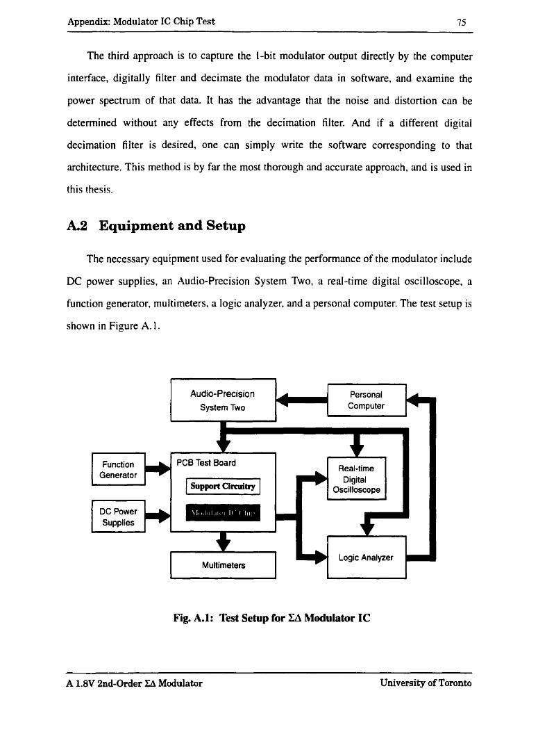
Appendix: Modulator IC Chip Test 75
The third approach is to capture the 1-bit modulator output directly by the computer
interface, digitally filter and decimate the modulator data in software, and examine the
power spectmm of that data. It has the advantage that the noise and distortion can be
determined without any effects from the decimation fiiter. And if a different digital
decimation filter is desired, one can simply wtite the software corresponding to that
architecture. This method is by far the most thorough and accurate approach, and is used in
this thesis.
A . Equipment and Setup
The necessary equipment used for evaluating the performance of the modulator include
DC power supplies, an Audio-Precision System Two, a real-time digital oscilloscope, a
function generator, multimeters, a logic analyzer, and a persona1 computer. The test setup is
shown in Figure A. 1.
Fig. A.l: Test Setup for LA Modulator IC
A 1.8V 2nd-Order ZA Modulator University of Toronto
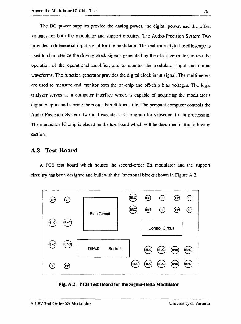
Appendix: Modulator IC Chip T ~ s t 76
The DC power supplies provide the analog power, the digital power, and the offset
voltages for both the modulator and support circuitry. The Audio-Precision System Two
provides a differentid input signal for the modulator. The real-time digital oscilloscope is
used to chancterize the driving clock signals generated by the clock generator, to test the
operation of the operational amplifier, and to monitor the modulator input and output
waveforms. The function generator provides the digital clock input signal. The multimeters
are used to rneasure and rnonitor both the on-chip and off-chip bias voltages. The logic
analyzer serves as a computer interface which is capable of acquiring the moduiator's
digital outputs and storing them on a harddisk as a file. The personai computer controls the
Audio-Precision System Two and executes a C-program for subsequent data processing.
The rnodulator IC chip is placed on the test board which will be descnbed in the following
section.
Test Board
A PCB test board which houses the second-order LA modulator and the support
circuitry has been designed and built with the functional blocks shown in Figure A.2.
Bias Circuit
8 / DIP40 Socket
1 Controi Circuit
Fig. A.2: PCB Test Board for the Sigma-Delta Modulator
A 1.8V 2nd-Order Li Modulator University of Toronto
Appendix: Modulator IC Chip Test 77
The DP40 socket holds the second-order ZA modulator IC chip. The bias circuit
provides the off-chip bias voltages for the modulator in case the on-chip bias circuit does
not work properly due to the process variations. This bias circuit is necessary especially in a
low-voltage design. The control circuit set the bias Ievels and the compensation capacitor
values for the operational amplifier. The BNC connectors are used to connect the input and
output analog/digital signals of the chip. The BP (binding post) connectors are used to
connect the power supply, and to monitor the bias voltages.
A4 Test procedure
k4.1 Bias Circuit Test
By adjusting the off-chip resistance, the bias voltages generated by the bias circuit were
measured using multimeters.
A.4.2 Clock Signals Test
A 2.56 MHz square wave clock signal. with proper offset voltage. was generited by the
function generator and was fed into the modulator's clock input. Using the real-time digital
oscilloscope, the eight-phase output cloc k signals were detected. The phase relationships
between them have been checked, and the overlapping penod, rise time, and faIl time were
measured.
A.4.3 Operational Ampiifier
The operational amplifier was set up in an inverting amplifier with the negative
feedback configuration. A fully-differential sine wave input signal with proper DC offset
voltage was generated by the Audio-Precision System Two, and was applied on the
amplifier's input. The oscilloscope was used to detect both the input and the output
waveforms of the amplifier in order to measure the close-loop gain. Increasing the input
- - - --- - - - -- - --
A 1.8V 2nd-Order Eî Modulator University of Toronto
Appendix: Modulator IC Chip Test 78
signal frequency up to the point where the output signal amplitude reaches 0.707 tirnes of
the original one cm find the cut-off frequency of the inverting amplifier. The intercepting
points of close-loop gain and cut-off frequency make up the frequency response of the
open-loop gain.
Setting the operational amplifier in a unity-gain feedback configuration, a sine input
with proper DC offset was applied on the opentional amplifier's input. The oscilloscope
was used to detect the phase shift between the input and output wavefonns to detect the
compensation result. With a large amplitude square wave applied on the input. the oparnp
output signal was detected, and the slew rate was measured using the oscilloscope.
k4.4 Characterizing the Modulator
%y using the persona1 computer to control the Audio-Precision System Two. a fully
differential sine wave signal with a proper DC offset has been generated and fed into the
rnodulator's input. With the proper on-chip bias voltages and well-compensated integrators.
the modulator has been tested functionally by using the oscilloscope to detect the pulse-
density-modulated digital outputs.
To evaluate the rnodulator performance, the original modulator digital output was
sampled by the logic analyzer and stored as files on the harddisk of the personal computer.
A C-program was created to perform the subsequent data processing. The full spectrum
calculations were performed in Matlab. By changing the input signal levels, the
corresponding SNR and SNDR were calculated. and the dynamic range was obtained.
A 1.8V 2nd-Order XA Modulator Universi@ of Toronto