Embed Size (px)
Citation preview
The 5th Power Electronics, Drive Systems and Technologies Conference (PEDSTC 2014), Feb 5-6, 2014, Tehran, Iran fljlPEDSYc-J'
A Bump-Less Multi-Level PI Controller for a Boost Converter
VahidF ereshtehpoor
Islamic Azad University Science & research Tehran
Branch
OmidNaghashAlmasi
Islamic Azad University Gonabad Branch
Mohammad Monfared
Ferdowsi University of Mashhad
v. [email protected] [email protected] [email protected]
Abstract-The boost converter is a non-minimal phase system with a right-half-plane zero in the transfer function. Accordingly, a slow dynamic controller is designed to control the converter. This paper proposes a bump-less multi-level PI control scheme for a DC-DC boost converter which ensures stability over a wide range of operating conditions and at the same time offers a high dynamic performance. Extensive comparative simulations with a conventional PI controller are then carried out to demonstrate the effectiveness of the proposed method. Simulation results show the superior control performance of the multi-level PI controller over the simple PI controller.
Keywords- Boostconverter; PI controller;multi-level control;bump-less control
1. INTRODUCTION
In many industrial applications, it is necessary to convert an unregulated DC input voltage into a regulated DC output voltage. DC-DC converters are used in personal computers, laptops, Personal Digital Assistants (PDAs), office appliances, aircrafts, satellite communication equipment and DC motor starting circuits [1, 2]. Therefore, there has been a growing interest in the development of efficient control strategies to improve dynamic behavior of DC-DC converters. There are different types of switching DC-DC converters, among which the boost regulator is used in applications where the output voltage should be higher than the input and the output polarity is the same as the input voltage [3]. The boost converter exhibits inherently non-linear dynamic behavior, as it is a non-minimum phase system with a zero in the right half plane [3, 4]. Thus, an important way to improve the performance of the closed loop converter system is the strategy of control. The boost converter consists of both linear (resistor, inductor and capacitor) and nonlinear (diode and active switch) components. The most common method to model power electronic converters is the state-space averaging approach [5, 6]. While this model is obtained for the boost converter, a non-linear equation is appeared, which first requires linearization around the operating point to obtain the small signal transfer function of the converter system. [n other words, the desired transfer function is only valid in vicinity of the operating point and for a small
978-1-4799-3479-9/14/$31.00 ©2014 IEEE
range of variations in system parameters. This would also be true for the controller designed based on the transfer function. As aforementioned, if a wide range of the output voltage is desired and because of the nonminimum phase characteristic of the transfer function of the boost converter, one will face severe restrictions in selecting a wide bandwidth for the controller. [n this paper, a new control scheme is proposed to control this converter. Unlike the previous control methods [7-9] and [10], the proposed method consists of a multi-level P[ controller to enhance the performance of the converter. That is, the proportional and integral coefficients of the PI controller vary depending on the operating point of the converter and the variation range of the output voltage. The optimal PI controller coefficients are designed based on the well-known frequency-response technique [11]. Suddenly changing the coefficients of the controllers generates drastic oscillations in the output voltage, which can deteriorate the performance of the converter. To prevent such oscillations, this study adopts the methods, which are proposed to switch the actuators from automatic to manual state and vice versa, extends it to the switching of the controllers in the power electronic converters. To realize this idea, the integral parts of PI controllers are modified. Consequently, a multi-level PI controller is proposed, which not only has better performance than the conventional one-level controllers, but also generates no oscillation while switching the coefficients of the controllers. The rest of this paper is organized as follows. [n section II, the linearized averaged state-space model of the boost converter is obtained and analyzed. Then, in section III, a multi-level PI controller is designed to control the boost converter. Some simulations are presented in support of the proposed controller in section IV. Finally, conclusions are drawn in section V.
2. LINEARIZED AVERAGEDSTATE SPACE MODEL
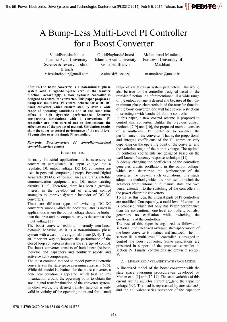
A linearized model of the boost converter with the state space averaging procedurewas developed by Mohan et al [1] and [12-[4]. The state variables of this circuit are the inductor current (Iind)and the capacitor voltage (Ve). The load is represented by aresistanceRL and the equivalent series resistance of the capacitor
518
L -
iind ic !
+ c +
VC RJ. Va
re
Figurel. Boost converter with the switch closed.
C is represented as reo
The output variables of the Boost converter are the line current (lune)and the output voltage(Vo)' The boost converter with closed switch is depicted in Fig. I. The state equations for Fig. I are:
(1)
The output equationis:
(2)
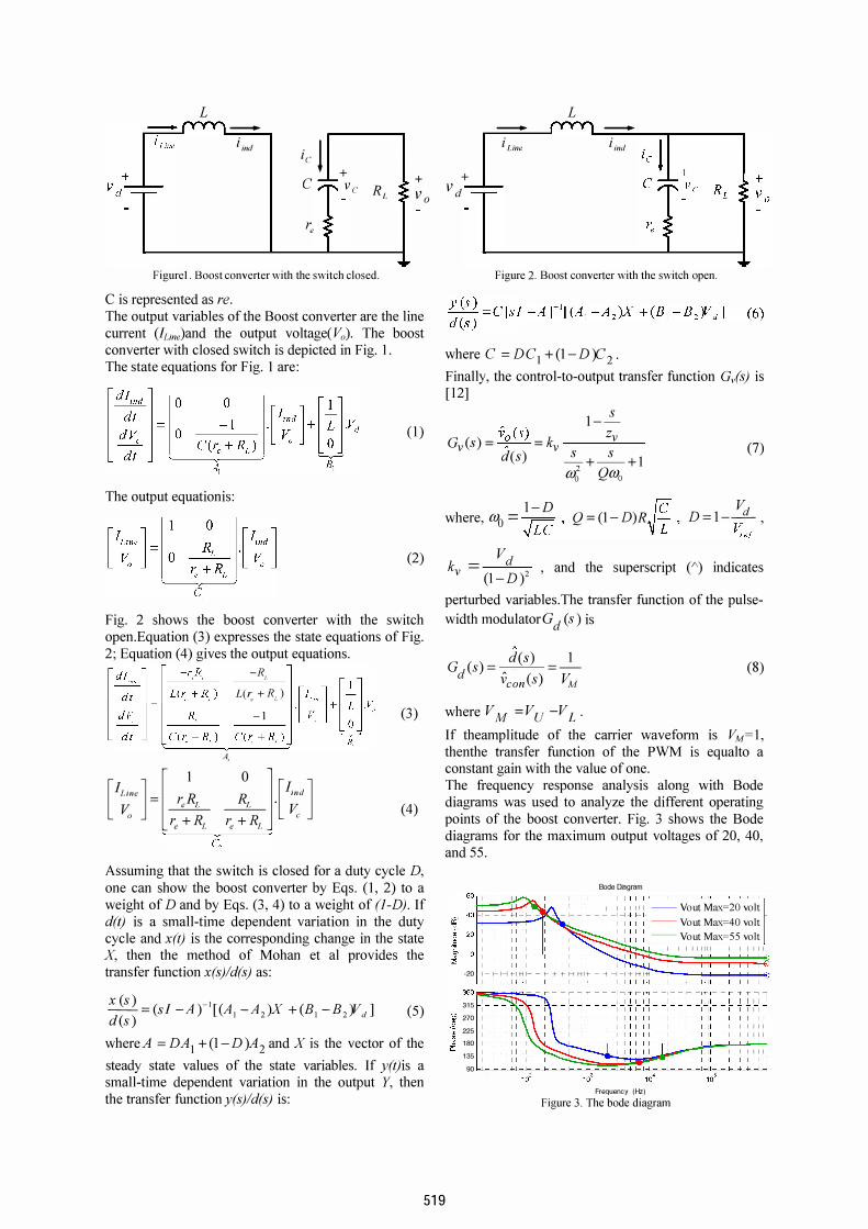
Fig. 2 shows the boost converter with the switch open. Equation (3) expresses the state equations of Fig. 2; Equation (4) gives the output equations.
-R,
r ?�' U r(�;�l l dt J lC(r,+R,) C(r,+R,)
L(/; + R,) -1
A,
[1�1C]=[� �l
.[l�d ]
re + Rr. re + Rr. . , (;2
(3)
(4)
Assuming that the switch is closed for a duty cycle D, one can show the boost converter by Eqs. (1, 2) to a weight of D and by Eqs. (3, 4) to a weight of (I-D). If d(t) is a small-time dependent variation in the duty cycle and x(tJ is the corresponding change in the state X, then the method of Mohan et al provides the transfer function x(s)/d(s) as:
x (s) -I --=(sl -A) [(A[-A2)X +(B[-B2)VdJ des)
(5)
whereA = DA I + (1-D )A2 and X is the vector of the
steady state values of the state variables. If y(tJis a small-time dependent variation in the output Y, then the transfer functiony(s)/d(s) is:
519
L - -
i Line iind
+ Vd
Figure 2. Boost converter with the switch open.
where C = Del + (1-D)C 2 . Finally, the control-to-output transfer function GJs) is [12]
1-� G (s)=
v�
(s) =k Zv
v des)
v s s -+--+1 OJ� QOJo
(7)
_I-D ft
Vd where, OJo - r;-;:; ' Q =(1-D)R -- , D=l-- , �LC L �4
V k =
d , and the superscript (/\) indicates v (I_D)2
perturbed variables. The transfer function of the pulse
width modulatorG d (s) is
G ()_ des) __ 1 d s - -
vcan (s) VM (8)
where V M =Vu -VL· If theamplitude of the carrier waveform is VM=I, thenthe transfer function of the PWM is equalto a constant gain with the value of one. The frequency response analysis along with Bode diagrams was used to analyze the different operating points of the boost converter. Fig. 3 shows the Bode diagrams for the maximum output voltages of 20, 40, and 55.
Bode Diagram
I "" II -- Vout Max�20 volt -- Vout Max�40 volt -- Vout Max�55 volt
I I I IIIIII I I I I II
-20 1- f-I-I +I+fl- - +- + + H HI+- - -+ -1-1 + 1-+1+1 c-'_�-r-+-................ _ ................. �
3� ������������--���--��� 315 : : : : : : 270 225 180
I I I I II I I I I II
I I I I II 135 rl�8::���1:::;��±�!:':::����-1:'�' �T�'-j" 90 bl
Frequency (I-\z) Figure 3. The bode diagram

L 100, Diode
1m I ----y;- -I Id r, + + Ie Vd Diode S g V"", "
I:z::
CT
Controller
Figure 4. The control scheme
As it can be seen, the transfer function of theboost converter has negative gain and phase margins, which makes it unstable when an appropriate controller is not used. In addition, it is clear that a change in the operating point causes a variation in the margin of stability. By evaluating the system transfer function we can find an unstable zero whose position depends on the inductor value, the inductor current, and the input voltage level. This unstable zero imposes some restrictions on the choice of a wide bandwidth for the controller. Moreover, the situation becomes worse as the output voltage increases, thus for maintaining the stability of the system a controller system with a slower dynamic is required.
3. CONTROL SCHEME
In this section, different parts of the proposed control scheme and the conventional control schemeare presented.
3.1. One-level PI controller As shown in the frequency analysis, the transfer function model changes relative to the different operating points. Thus, using a controller for the converter in a wide range of output voltage changes can degrade the performance of the converter in some operating points. Increasing the output voltage will restrict the selected bandwidth of the controller to achieve a stable system. Therefore, the controller in the low output voltages can have a wider bandwidth. According to the above explanations, designing a single controller for all operating points requires to consider the worst-condition system (which occurs in the maximum output voltage given the consistency of the load resistance). As a result, it is obvious that theboost converter is designed for the maximum output voltage and it will not have a fast dynamic behavior at low output voltages.
3.2. Multi-level PI controller A. With oscillations in output voltage
Figure 5. Schematic model of the classic PI controller
The proposed method resolves the above problem by using distinct PI controller parameters for different operating points. To this purpose, an optimal PI controller is designed for each range of the output voltage variations based on the frequency response technique. The output voltage level of the converter is always compared to the preset values, i.e. Vu and Vu (the replacement points of the controller coefficients), thus the optimal coefficients of the PI controller are selected based on the output voltage level. Finally, the controller output goes to the PWM pulse generator and determines the state of the switch S. The scheme of theboost converter in presence of the proposed control system is shown in Fig. 4. In Fig. 4, Vctrlt) is the controller output, Vcalt) is the carrier waveform of the PWM pulse generator, ere/t) is the error signal, which is the difference between the reference signal and the system outputvoltage, and Ki and Kp are proportional and integral gains of the optimal PI controller, respectively. Fig. 5 shows the schematic model of the PI controller and Fig. 6 shows the scheme of the multi-level PI controller. Switching the coefficients of the PI controllers produces severe oscillations in the output voltage, which can hamper the stabilization of the positive points of the proposed method. Such oscillations are caused by the successive replacement of the controller gains in the points where the output voltage is close to Vu and Vu. E. Without oscillation in output voltage The oscillations in the output voltage are caused by the existing significant difference between the outputs of the controllers at each level at any moment. :-------====�------�
: LEVEL I \----:1 ��I � � I' I I I ......... .......... I I eLi
� ------------______ I
Figure 6. Schematic model of the multi-level PI controller
520
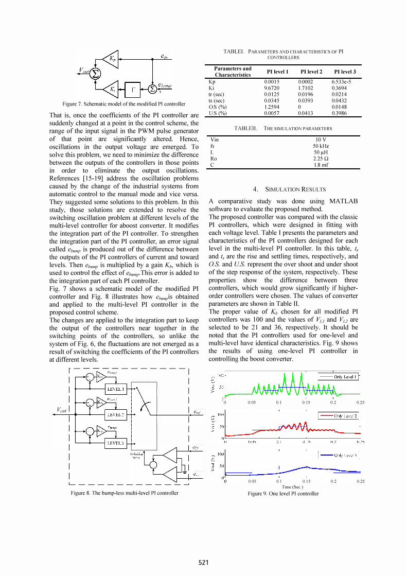
Figure 7. Schematic model of the modified PI controller
That is, once the coefficients of the P[ controller are suddenly changed at a point in the control scheme, the range of the input signal in the PWM pulse generator of that point are significantly altered. Hence, oscillations in the output voltage are emerged. To solve this problem, we need to minimize the difference between the outputs of the controllers in those points in order to eliminate the output oscillations. References [[ 5-[9] address the oscillation problems caused by the change of the industrial systems from automatic control to the manual mode and vice versa. They suggested some solutions to this problem. [n this study, those solutions are extended to resolve the switching oscillation problem at different levels of the multi-level controller for aboost converter. It modifies the integration part of the PI controller. To strengthen the integration part of the PI controller, an error signal called ehllmp is produced out of the difference between the outputs of the PI controllers of current and toward levels. Then ebump is multiplied by a gain Kb, which is used to control the effect of ebllmp.This error is added to the integration part of each P[ controller. Fig. 7 shows a schematic model of the modified P[ controller and Fig. 8 illustrates how ebum)S obtained and applied to the multi-level P[ controller in the proposed control scheme. The changes are applied to the integration part to keep the output of the controllers near together in the switching points of the controllers, so unlike the system of Fig. 6, the fluctuations are not emerged as a result of switching the coefficients of the PI controllers at different levels.
r - - - ----;'h,,-::; - - - - - - - I I
+- KhJ r····················: I
i I Vetrl I
\i I
. i Ie,,; i I i I ! I
t.. _______ _________ .J
L- ___________ ----l
Figure 8. The bump-less multi-level PI controller
521
TABLEI. PARAMETERS AND CHARACTERISTICS OF PI CONTROLLERS
Parameters and Characteristics
Kp Ki tr(sec) ts (sec) O.S (%) U.S (%)
PI level 1 0.0015 9.6720 0.0125 0.0345 l.2594 0.0057
PI level 2 0.0002 1.7102 0.0196 0.0393 o 0.0413
TABLEII. THE SIMULATION PARAMETERS
Yin 10 V fs 50 kHz L 50�H � 2�O C l.8 mf
4. SIMULATION RESULTS
PI level 3 6.533e-5 0.3694 0.0214 0.0432 0.0148 0.3986
A comparative study was done using MATLAB software to evaluate the proposed method. The proposed controller was compared with the classic P[ controllers, which were designed in fitting with each voltage level. Table [ presents the parameters and characteristics of the P[ controllers designed for each level in the multi-level PI controller. In this table, tr and t, are the rise and settling times, respectively, and o.s. and us. represent the over shoot and under shoot of the step response of the system, respectively. These properties show the difference between three controllers, which would grow significantly if higherorder controllers were chosen. The values of converter parameters are shown in Table [I. The proper value of Kb chosen for all modified P[ controllers was 100 and the values of Vu and Vu are selected to be 2 [ and 36, respectively. [t should be noted that the P[ controllers used for one-level and multi-level have identical characteristics. Fig. 9 shows the results of using one-level PI controller in controlling the boost converter.
f:�[ ��'''1 o 0.05 0.1 0.15 0.2 0.25
f:o�t ========-;;-------'------I -�I"", �," j 0.05 0.1 0.15 0.2 0.25
Time (Sec.) Figure 9. One level PI controller
(a)
j o·� f IlIImll
o-------o� .0�5WU�U-�0.-I------0�. 1 -5 ------�0.2-------0-.25 (b)
] o � f IIIIIIJaOOIIOOI 0L-------0.0·5�UIUL� 0.lll�ruwillllOru.lrn5illll�ruwruO.�2�----0�.25 (e)
j o � f 11111111 I�I 0L-----�0.0-5��LL� 0.ul�ru( drn) illll O�.lill5rnwillllWilllliO.2�L----0-.25 rime (Sec.)
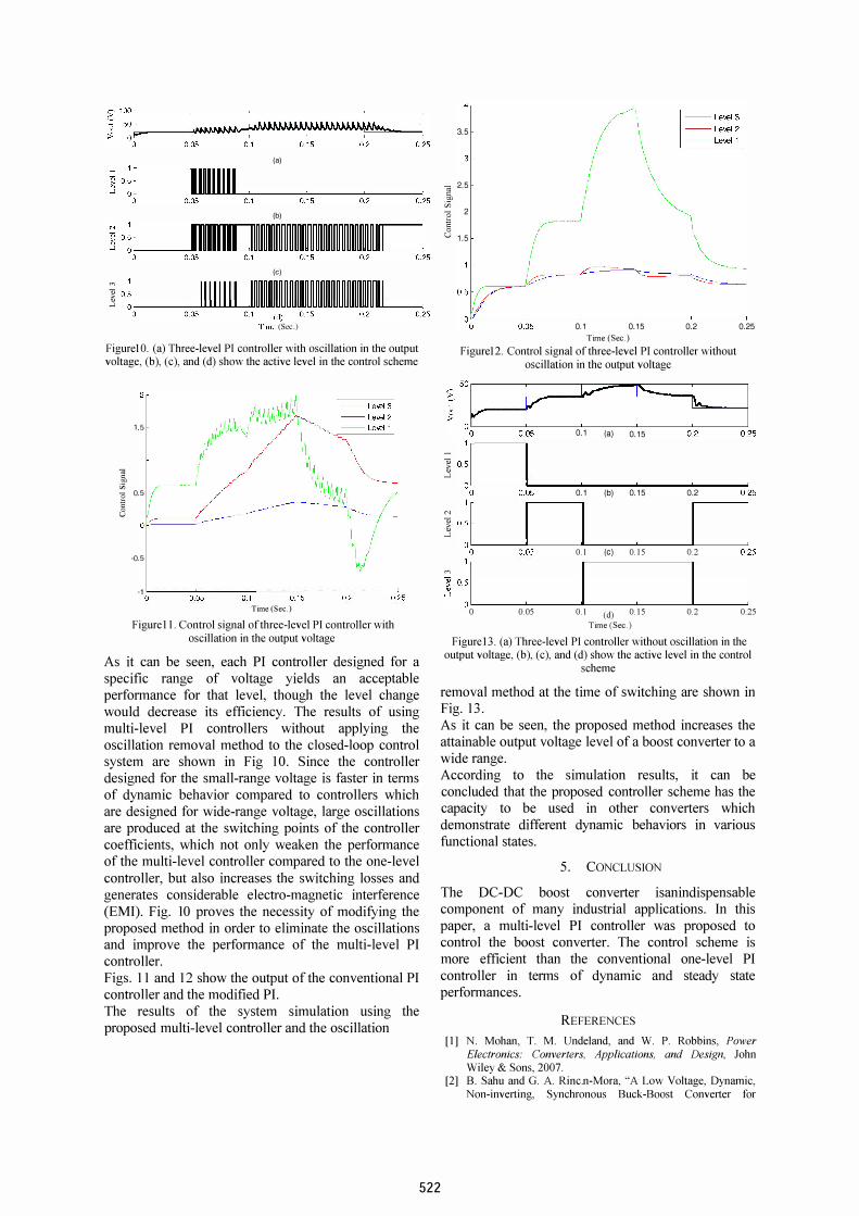
FigurelO. (a) Three-level PI controller with oscillation in the output voltage, (b), (c), and (d) show the active level in the control scheme
1.5
" � (3 0.5 � u
-0.5
-1 0:------0::-'.0::::5----�0.-:-1 -----0 �.1-5 ----- 0�.2---------J0.25 Time (Sec.)
Figurell. Control signal of three-level PI controller with oscillation in the output voltage
As it can be seen, each PI controller designed for a specific range of voltage yields an acceptable performance for that level, though the level change would decrease its efficiency. The results of using multi-level PI controllers without applying the oscillation removal method to the closed-loop control system are shown in Fig 10. Since the controller designed for the small-range voltage is faster in terms of dynamic behavior compared to controllers which are designed for wide-range voltage, large oscillations are produced at the switching points of the controller coefficients, which not only weaken the performance of the multi-level controller compared to the one-level controller, but also increases the switching losses and generates considerable electro-magnetic interference (EMI). Fig. 10 proves the necessity of modifying the proposed method in order to eliminate the oscillations and improve the performance of the multi-level P[ contro II er. Figs. 1 [ and [2 show the output of the conventional P[ controller and the modified PI. The results of the system simulation using the proposed multi-level controller and the oscillation
522
4
3.5
ca 2.5 c '"
en -0 2 -E o u 1.5
0.1 0.15 0.2 Time (Sec.)
Figurel2. Control signal of three-level PI controller without oscillation in the output voltage
0.1 (a) 0.15
0.25
] ":1 oL-----�------�------�------�----�0.25 0.1 (b) 0.15 0.2
] ";1 0�----��----�------�------J-----�0.25 I I 0.05 0.1 (e) 0.15 0.2
�. 1 [ ]
0 : ,-[ ______ � ______ ""___ ____ � ______ ----L ______ __i I I a 0.05 0.1 (d) 0.15 0.2 0.25
Time (Sec.) Figure 13. (a) Three-level PI controller without oscillation in the
output voltage, (b), (c), and (d) show the active level in the control scheme
removal method at the time of switching are shown in Fig. [3. As it can be seen, the proposed method increases the attainable output voltage level of a boost converter to a wide range. According to the simulation results, it can be concluded that the proposed controller scheme has the capacity to be used in other converters which demonstrate different dynamic behaviors in various functional states.
5. CONCLUSION
The DC-DC boost converter isanindispensable component of many industrial applications. [n this paper, a multi-level P[ controller was proposed to control the boost converter. The control scheme is more efficient than the conventional one-level P[ controller in terms of dynamic and steady state performances.
REFERENCES
[I] N. Mohan, T. M. Undeland, and W. P. Robbins, Power Electronics: Converters. Applications, and Design, John Wiley & Sons, 2007.
[2] B. Sahu and G. A. Rinc.n-Mora, "A Low Voltage, Dynamic, Non-inverting, Synchronous Buck-Boost Converter for

Portable Applications, " IEEE Trans. Power Electron., vol. 19, no. 2, Mar. 2004.
[3] V. I. Utkin, "Sliding Mode Control Design Principles and Applications to Electric Drives, " IEEE Trans.lndustrial Electronics, vol. 40, no. I, pp. 23-36.
[4] D. C. Hamill, D. 1. Jefferies, "Subharmonics and chaos in a controlled switched-mode power converter, " IEEE Trans Circ. Syst., vol. 3S, no.8,pp. lOS9-61, 1998.
[S] S. K. Mazumder, A. H. Nayfeh, and D. Boroyevich, 'Theoretical and experimental investigation of the fast and slow-scale instabilities of a DC-DC converter, " IEEE Trans. Power Electron., vol. 16, pp. 201-216, 2001.
[6] .R. D. Middlebrook, S. Cuk, "A general unified approach to modelling switching-converter power stages, " In Power Electronics Specialists Conference vol. I, pp. 18-34, 1976.
[7] G. K. Andersen and F. Blaabjerg, "Current Programmed Control of a Single-Phase Two-Switch Buck-Boost Power Factor Correction Circuit, " IEEE Trans. Industrial Electron., vol. S3, no. I, Feb. 2006.
[8] C. Restrepo, 1. Calvente, A. Cid-Pastor, A. E. Aroudi, and R. Giral, "A Noninverting Buck-Boost DC-DC Switching Converter With High Efficiency and Wide Bandwidth, " IEEE Trans. Power Electron., vol. 26, no.9, pp.2490-2S03, Sept. 2011.
[9] J.-K. Shiau and C.-J. Cheng, "Design of A Non-Inverting Synchronous Buck-Boost DC/DC Power Converter With Moderate Power Level, " Robotics and Computer-Integrated Manufacturing, vol. 26, no. 3, 2010.
[10] Y. Lee, A. Khaligh, and A. Emadi, "A Compensation Technique for Smooth Transitions in a Non-inverting BuckBoost Converter, " IEEE Trans. Power Electron., vol. 24, no. 4, Apr. 2009.
[11] K. Ogata, Modern control engineering, Prentice Hall, Sth ed., 2010.
[12] M. Alfayyoumi, A. H. Nayfeh, and D. Borojevic, "Modeling and analysis of switching-mode DC-DC regulators, " International Journal of Bifurcation and Chaos, vol. 10, pp. 373-390, 2000.
[13] N. Kondrath, and M. K. Kazimierczuk, "Control-to-output transfer function of peak current-mode controlled PWM DCDC Boost converter in CCM. Electronics letters, vol. 47, no.17, 991-993, 2011.
[14] X.P. Yang, H. Zhang, and X.K. Ma, "Modeling and stability analysis of cascade buck converters with N power stages,"Mathematics and Computers in Simulation, vol. 80, pp.S33-S46, 2009.
[IS] K. J. Astrom and B. Wittenmark, Computer-Controlled Systems, Theory and Design, 3rd Ed., Prentice-Hall, Inc., 1997.
[16] S. F. Graebe and A. 1.. B. Ahlen, "Dynamic Tranfer Among Alternative Controllers and Its Realtion to Anti-Windup Controller design, IEEE Trans. Control Sys. Tech., vol. 4, pp. 92-99, 1996.
[17] L. Zaccarian and A. R. Teel, "The L2 (12) bumpless transfer problem for linear plants: its definition and solution, " Automatica, vol. 41, pp.1273-1280, 200S.
[18] I. Malloci, L. Hetel, 1. Daafouz, C. lung, and P. Szczepanski, "Bumpless transfer for switched linear systems, " Automatica, vo1.48, no.7, pp. 1440-1446, Jul. 2012.
[19] 1.-1. Yame, and Q. Hanping, "Conditioned switching between two-degree-of-freedom controllers for plants with changing dynamics, " IEEE Conf Control Automation Robotics & Vision (ICARCV), pp.94S-9SI, Dec. 2010.
523

![IPv4 to IPv6 Bump In Stack - Home | Lancaster University · IPv4 to IPv6 Bump In Stack ... A \bump in the stack"[56] at its highest level overview is a ... The allocation of this](https://img.pdfslide.net/doc/110x75/5ad16e4a7f8b9afa798ba5b1/ipv4-to-ipv6-bump-in-stack-home-lancaster-to-ipv6-bump-in-stack-a-bump.jpg)