Embed Size (px)
Citation preview

CMT2189C
Rev 0.8 | Page1/35 www.cmostek.com
A
CMT2189C 240 – 960 MHz SoC (G)FSK/OOK Transmitter
Copyright © By CMOSTEK
Features
High-Performance RISC CPU
PIC16-likeInstruction-set
Only 37 instructions to learn:
- All Single-Cycle Except Branches
Operating speed:
- Up to 16 MHz Clock
- 125nsinstruction cycle
- FSYS = 8MHz @ 2.0V~3.6V
- FSYS = 16MHz @ 2.7V~3.6V
Interrupt capability
8-level deep hardware stack
2048 Words Flash / 128B SRAM / 256B EEPROM
2 x 8-bit timers/counters with programmable prescaler
4 I/O pins with individual direction control:
- Interrupt-on-pin change
- Individually programmable weak pull-ups
- Push-pull output except PA5
Applications
Remote Keyless Entry (RKE)
Garage and gate door openers
Home/Building Automation and Security
Industrial Monitoring and Controls
Remote Lighting Control
Wireless Alarm and Security Systems
Consumer Electronics Applications
Descriptions
The CMT2189C devices are fully integrated, highly flexible,
high performance, SoC (G)FSK/OOK transmitters with
embedded RISC microcontroller core for various 240 to 960
MHz wireless applications. They are part of the CMOSTEK
NextGenRFTM family, which includes a complete line of
transmitters, receivers and transceivers. The CMT2189C
uses a 1-pin crystal oscillator circuit with the required crystal
load capacitance integrated on-chip to minimize the BOM
counts. The device can deliver up to +13 dBm output power
and the PA output can be either single-ended or differential.
The device operates from 2.0 V to 3.6 V. Its low power
design enables superior operation life for battery powered
application. The CMT2189C transmitter together with
CMOSTEK NextGenRFTM receiver enables a highly flexible,
low cost RF link.
SOP14
Ordering Information
Part Number Frequency Package Option MOQ
CMT2189C-ESR 868.35 MHz T&R 2,500 pcs
CMT2189C-ESB 868.35 MHz Tube 1,000 pcs
More Ordering Info: See Page 30
High-Performance OOK Transmitter
All Features Configurable
Frequency Range: 240 to 960 MHz
FSK, GFSK and OOK Modulation
Symbol Rate up to 100 kbps
Configurable Single-Ended or Differential PA Output
Output Power:-10 to +13 dBm
Supply Voltage: 2.0 to 3.6 V
FCC / ETSI Compliant
RoHS Compliant
14-pin SOP Package
1
2
3
4
5
6
7 8
9
10
11
12
13
14AVDD
GND
PAP
PAN
PC2/RFCLK
PA5/MCLRB
PA2/T0CKI/INT
XTAL
GND
PC4/RFDAT
DVDD
GND
PA1/ICSPDAT
PA0/ICSPCLK
CMT2189C

CMT2189C
Rev 0.8 | Page2/35 www.cmostek.com
Typical Application
U1
XTALAVDD
GND GND
1
X1
PC4/RFDATPAP
CMT2189C
DVDDPAN
PC2/RFCLK GND
2
3
4
5
6
7
14
13
12
11
10
9
8
RFCLK
VDD
Loop Antenna
RFDAT
J1VDD
1
2
3
4
SW0
SW1SW2
SW3
C0
L1
C2 VDDC1
PA5/MCLRB
PA2 PA0/ICSPCLK
PA1/ICSPDAT
PA1/ICSPDAT
PA0/ICSPCLK
Notes:
1. Connector J1 is ICSP
Debugger Interface
Figure 1.CMT2189C Typical Application with Differential PA Output
Table 1.BOM of 868.35 MHz Application with Differential PA Output
Designator Descriptions Value Unit Manufacturer
U1 CMT2189C, 240 – 960 MHz SoC(G) FSK/OOK transmitter - - CMOSTEK
X1 ±20 ppm, SMD32*25 mm crystal 26 MHz EPSON
SW[3:0] Push buttons - -
D1 MBR0520LT1, SOD123 (Optional) - - IR
R1 ±5%, 0402 10 kΩ
C0 ±20%, 0402 X7R, 25 V 0.1 uF Murata GRM15
C1 ±0.25 pF, 0402 NP0, 50 V 2.2 pF Murata GRM15
C2 ±0.25 pF, 0402 NP0, 50 V 1.5 pF Murata GRM15
L1 ±5%, 0603 multi-layer chip inductor 100 nH Murata LQG18
U1
1
X1CMT2189C
2
3
4
5
6
7
14
13
10
9
8
CLK
VDD
VTG
CLK2
DATA2 SW0
SW1SW2
SW3
C0
L1
L2
C2
C1
ANT
L3
C3
12
11
DATA
VDD
AVDD
GND
PAP
PAN
PC2/RFCLK
PA5/MCLRB
PA2
J1VDD
1
2
3
4
PA1/ICSPDAT
PA0/ICSPCLK
XTAL
GND
PC4/RFDAT
DVDD
GND
PA0/ICSPCLK
PA1/ICSPDAT
Notes:
1. Connector J1 is ICSP
Debugger Interface
Figure 2. CMT2189C Typical Application with Single-ended PA Output

CMT2189C
Rev 0.8 | Page3/35 www.cmostek.com
Table 2. BOM of868.35 MHz Application with Single-ended PA Output
Designator Descriptions Value Unit Manufacturer
U1 CMT2189C, 240 – 960 MHz SoC (G)FSK/OOK transmitter - - CMOSTEK
X1 ±20 ppm, SMD32*25 mm crystal 26 MHz EPSON
SW[3:0] Push buttons - -
D1 MBR0520LT1, SOD123 (Optional) - - IR
R1 ±5%, 0402 10 kΩ
C0 ±20%, 0402 X7R, 25V 0.1 uF Murata GRM15
C1 ±5%, 0402 NP0, 50V 68 pF Murata GRM15
C2 ±5%, 0402 NP0, 50V 9.1 pF Murata GRM15
C3 ±5%, 0402 NP0, 50V 8.2 pF Murata GRM15
L1 ±5%, 0603 multi-layer chip inductor 100 nH MurataLQG18
L2 ±5%,0603 multi-layer chip inductor 8.2 nH MurataLQG18
L3 ±5%,0603 multi-layer chip inductor 8.2 nH MurataLQG18

CMT2189C
Rev 0.8 | Page4/35 www.cmostek.com
Abbreviations
Abbreviations used in this data sheet are described below
AN Application Notes NP0 Negative-Positive-Zero
BOM Bill of Materials OBW Occupied Bandwidth
BSC Basic Spacing between Centers OOK On-Off Keying
BW Bandwidth PA Power Amplifier
DC Direct Current PC Personal Computer
EEPROM Electrically Erasable Programmable Read-Only
Memory
PCB Printed Circuit Board
PLL Phase Lock Loop
ESD Electro-Static Discharge PN Phase Noise
ESR Equivalent Series Resistance RBW Resolution Bandwidth
ETSI
European Telecommunications Standards
Institute
RCLK Reference Clock
RF Radio Frequency
FCC Federal Communications Commission RFPDK RF Product Development Kit
FSK Frequency Shift Keying RoHS Restriction of Hazardous Substances
GFSK Gauss Frequency Shift Keying Rx Receiving, Receiver
GUI Graphical User Interface SOT Small-Outline Transistor
IC Integrated Circuit TBD To Be Determined
LDO Low Drop-Out Tx Transmission, Transmitter
Max Maximum Typ Typical
MCU Microcontroller Unit XO/XOSC Crystal Oscillator
Min Minimum XTAL Crystal
MOQ Minimum Order Quantity

CMT2189C
Rev 0.8 | Page5/35 www.cmostek.com
Table of Contents
Typical Application .................................................................................................................................................................... 1
1. Electrical Characteristics ................................................................................................................................................... 7
1.1 Recommended Operating Conditions ................................................................................................................... 7
1.2 Absolute Maximum Ratings................................................................................................................................... 7
1.3 Transmitter Specifications ..................................................................................................................................... 8
1.4 RF Crystal Oscillator ............................................................................................................................................. 9
1.5 Internal High Frequency Oscillator ........................................................................................................................ 9
1.6 Internal Low Frequency Oscillator ......................................................................................................................... 9
1.7 LVD/LVR ............................................................................................................................................................. 10
1.8 POR .................................................................................................................................................................... 10
1.9 I/O PAD ............................................................................................................................................................... 10
1.10 MCU Supply Current ........................................................................................................................................... 10
2. Pin Descriptions ................................................................................................................................................................ 11
3. Typical Performance Characteristics ............................................................................................................................. 12
4. Typical Application Schematics ...................................................................................................................................... 13
4.1 Typical Application with Differential PA Output ................................................................................................... 13
4.2 Typical Application with Single-ended PA Output ............................................................................................... 14
5. Functional Descriptions ................................................................................................................................................... 15
5.1 Overview ............................................................................................................................................................. 15
5.2 Modulation, Frequency, Deviation and Symbol Rate .......................................................................................... 15
5.3 Power Amplifier ................................................................................................................................................... 16
5.4 PA Ramping ........................................................................................................................................................ 16
5.5 Crystal Oscillator and RCLK................................................................................................................................ 17
6. RF Working States and Control Interface ...................................................................................................................... 18
6.1 Working States .................................................................................................................................................... 18
6.2 Transmission Control Interface ........................................................................................................................... 18
6.2.1 Tx Enabled by DATA Pin Falling Edge ............................................................................................... 19
6.2.2 Tx Enabled by DATA Pin Rising Edge ................................................................................................ 19
6.2.3 Two-wire Interface(TWI) ..................................................................................................................... 19
7. RISC Microcontroller Core ............................................................................................................................................... 22
7.1 Memory Organization .......................................................................................................................................... 23
7.1.1 Program Memory Organization .......................................................................................................... 23
7.1.2 Data Memory Organization ................................................................................................................ 23
7.1.2.1 General Purpose Register File ........................................................................................................... 23
7.1.2.2 Special Function Register File ............................................................................................................ 23
7.2 Port A .................................................................................................................................................................. 26
7.2.1 PORTA and the CPIOA Registers ...................................................................................................... 27
7.2.2 Additional Pin Functions ..................................................................................................................... 27

CMT2189C
Rev 0.8 | Page6/35 www.cmostek.com
7.2.2.1 Pull-up ................................................................................................................................................ 27
7.2.2.2 Interrupt-On-Change .......................................................................................................................... 27
7.3 PORTC ............................................................................................................................................................... 27
7.4 Timer0 Module .................................................................................................................................................... 28
7.4.1 Timer0 Operation ............................................................................................................................... 28
7.4.2 Timer0 Interrupt .................................................................................................................................. 28
7.4.3 Using Timer0 with an External Clock .................................................................................................. 29
7.4.4 Prescaler ............................................................................................................................................ 29
7.5 Timer2 Module .................................................................................................................................................... 29
8. Ordering Information......................................................................................................................................................... 30
9. Package Outline ................................................................................................................................................................. 31
10. Top Marking ........................................................................................................................................................................ 32
10.1 CMT2189C Top Marking ..................................................................................................................................... 32
11. Other Documentations ...................................................................................................................................................... 33
12. Document Change List ..................................................................................................................................................... 34
13. Contact Information .......................................................................................................................................................... 35

CMT2189C
Rev 0.8 | Page7/35 www.cmostek.com
1. Electrical Characteristics
VDD = 3.3 V, TOP = 25 ℃, FRF = 868.35 MHz, FSK modulation, output power is +10 dBm terminated in a matched 50 Ω
impedance with single-ended PA output, unless otherwise noted.
1.1 Recommended Operating Conditions
Table 3. Recommended Operation Conditions
Parameter Symbol Conditions Min Typ Max Unit
Operation Voltage Supply VDD 2.0 3.6 V
Operation Temperature TOP -40 85 ℃
Supply Voltage Slew Rate 1 mV/us
1.2 Absolute Maximum Ratings
Table 4. Absolute Maximum Ratings[1]
Parameter Symbol Conditions Min Max Unit
Supply Voltage VDD -0.3 3.6 V
Interface Voltage VIN -0.3 VDD +0.3 V
Junction Temperature TJ -40 125 ℃
Storage Temperature TSTG -50 150 ℃
Soldering Temperature TSDR Lasts at least 30 seconds 255 ℃
ESD Rating Human Body Model (HBM) -2 2 kV
Latch-up Current @ 85 ℃ -100 100 mA
Note:
[1]. Stresses above those listed as “absolute maximum ratings” may cause permanent damage to the device. This is a stress
rating only and functional operation of the device under these conditions is not implied. Exposure to maximum rating
conditions for extended periods may affect device reliability.
Caution! ESD sensitive device. Precaution should be used when handling the device in order
to prevent permanent damage.
CMT2189C
Rev 0.8 | Page8/35 www.cmostek.com
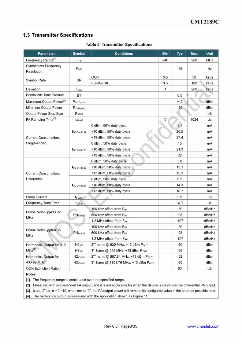
1.3 Transmitter Specifications
Table 5. Transmitter Specifications
Parameter Symbol Conditions Min Typ Max Unit
Frequency Range[1] FRF 240 960 MHz
Synthesizer Frequency
Resolution FRES 198 Hz
Symbol Rate SR
OOK 0.5 30 ksps
FSK/GFSK 0.5 100 ksps
Deviation FDEV 1 200 ksps
Bandwidth-Time Product BT 0.5 -
Maximum Output Power[2] POUT(Max) +13 dBm
Minimum Output Power POUT(Min) -10 dBm
Output Power Step Size PSTEP 1 dB
PA Ramping Time[3] tRAMP 0 1024 us
Current Consumption,
Single-ended
IDD-S-433.92
0 dBm, 50% duty cycle 9.1 mA
+10 dBm, 50% duty cycle 20.5 mA
+13 dBm, 50% duty cycle 27.4 mA
IDD-S-868.35
0 dBm, 50% duty cycle 10 mA
+10 dBm, 50% duty cycle 21.3 mA
+13 dBm, 50% duty cycle 28 mA
Current Consumption,
Differential
IDD-D-433.92
0 dBm, 50% duty cycle 5.8 mA
+10 dBm, 50% duty cycle 13.1 mA
+13 dBm, 50% duty cycle 15.3 mA
IDD-D-868.35
0 dBm, 50% duty cycle 6.5 mA
+10 dBm, 50% duty cycle 14.3 mA
+13 dBm, 50% duty cycle 16.7 mA
Sleep Current ISLEEP 2.5 uA
Frequency Tune Time tTUNE 370 us
Phase Noise @433.92
MHz PN433.92
100 kHz offset from FRF -80 dBc/Hz
600 kHz offset from FRF -98 dBc/Hz
1.2 MHz offset from FRF -107 dBc/Hz
Phase Noise @868.35
MHz PN868.35
100 kHz offset from FRF -80 dBc/Hz
600 kHz offset from FRF -98 dBc/Hz
1.2 MHz offset from FRFl -107 dBc/Hz
Harmonics Output for 315
MHz[4]
H2315 2nd harm @ 630 MHz, +13 dBm POUT -60 dBm
H3315 3rd harm @ 945 MHz, +13 dBm POUT -65 dBm
Harmonics Output for
433.92 MHz[4]
H2433.92 2nd harm @ 867.84 MHz, +13 dBm POUT -52 dBm
H3433.92 3rd harm @ 1301.76 MHz, +13 dBm POUT -60 dBm
OOK Extinction Ration 60 dB
Notes:
[1]. The frequency range is continuous over the specified range.
[2]. Measured with single-ended PA output, and it is not applicable for when the device is configured as differential PA output.
[3]. 0 and 2n us, n = 0 ~10, when set to “0”, the PA output power will ramp to its configured value in the shortest possible time.
[4]. The harmonics output is measured with the application shown as Figure 11.

CMT2189C
Rev 0.8 | Page9/35 www.cmostek.com
1.4 RF Crystal Oscillator
Table 6. Crystal Oscillator Specifications
Parameter Symbol Conditions Min Typ Max Unit
Crystal Frequency[1] FXTAL 26 26 26 MHz
Crystal Tolerance[2] ±20 ppm
Load Capacitance[3] CLOAD 12 20 pF
Crystal ESR Rm 60 Ω
XTAL Startup Time[4] tXTAL 400 us
Notes:
[1]. The CMT2189C can directly work with external 26 MHz reference clock input to XTAL pin (a coupling capacitor is
required) with amplitude 0.3 to 0.7 Vpp.
[2]. This is the total tolerance including (1) initial tolerance, (2) crystal loading, (3) aging, and (4) temperature dependence.
The acceptable crystal tolerance depends on RF frequency and channel spacing/bandwidth.
[3]. The required crystal load capacitance is integrated on-chip to minimize the number of external components.
[4]. This parameter is to a large degree crystal dependent.
1.5 Internal High Frequency Oscillator
Table 7. IHRC Specifications
Parameter Symbol Conditions Min Typ Max Unit
IHRC Frequency
FIHRC 3.3V, 27℃ 15.99 MHz
Temperature-dependent -20℃~ +80℃, 3.3V 4.2%/100℃
Voltage-dependent
2~3.6V ±3 %/V
Setup Time 2.2 10 us
Leakage Current
0.8 2 nA
Triming Range
Step 0.625% ±20%
1.6 Internal Low Frequency Oscillator
The ILRCsupport two frequency: 32KHz or 256KHz. It can be selected by LFMOD in OSCCON register, 0 is
the 32KHz, and the 1 is the 256KHz.
Table 8. ILRC Specifications
Parameter Symbol Conditions Min Typ Max Unit
ILRC Frequency
FILRC
2.5V, 25℃, 32K 32.3 KHz
2.5V, 25℃, 256K 258.5 KHz
Temperature-dependent -20℃~ +80℃, 2.5V 22.3%/100℃
Voltage-dependent
2~3.6V ±11.1 %/V
Setup Time 2.5V, 25℃ 4.6 10 us
Leakage Current
Disable 0.15 1 nA

CMT2189C
Rev 0.8 | Page10/35 www.cmostek.com
1.7 LVD/LVR
Table 9. LVD/LVR Specifications
Parameter Symbol Conditions Min Typ Max Unit
LVD Voltage
2.0
V 2.2
2.8
LVR delay
125 157 us
1.8 POR
Table 10. POR Specifications
Parameter Symbol Conditions Min Typ Max Unit
POR Current IPOR 3.3V 50 nA
Temperature-dependent
3.3V 2.0 V
1.9 I/O PAD
Table 11. I/OPAD Specifications
Parameter Symbol Conditions Min Typ Max Unit
Input Low Voltage VIL 0.3 VDD
Input High Voltage VIH 0.7 VDD
Output High Current IOH 3.3V, 25℃ 10 mA
Output Low Current IOL 3.3V, 25℃ 15 mA
Weak Pull-up 3.3V 41.7 KΩ
1.10 MCU Supply Current
Table 12. Supply Current
Parameter Symbol Conditions Min Typ Max Unit
Operation Mode 3.3V, FSYS = 2MHz 310 uA
3.3V, FSYS = 32KHz 50 uA
Sleep Mode with WDT_ON 3.3V 3 uA
Sleep Mode with WDT_OFF 3.3V 0.8 uA
Sleep Mode with LVD_ON 3.3V 15 uA
Notes:
1. All the IO is input mode, and with pull-down resistance.
2.Comparator is disable, CM<2:0> = 111

CMT2189C
Rev 0.8 | Page11/35 www.cmostek.com
2. Pin Descriptions
AVDD
GND
PAP
PAN
PC2/RFCLK
PA5/MCLRB
PA2/T0CKI/INT
DVDD
GND
XTAL
PA1/ICSPDAT
PA0/ICSPCLK
1
2
3
4
5
6
7
9
14
13
12
11
10
8
PC4/RFDAT
GND
Figure 3.CMT2189C Pin Assignments
Table 13.CMT2189C Pin Descriptions
Pin Number Name I/O Descriptions
1 AVDD I RF power supply input
2 GND I Ground
3 PAP O The differential power amplifier output, when using as singled-ended output, PAN/PAP
should be connected together before connecting to the matching network 4 PAN O
5 PC2/RFCLK IO PC2 PORTC I/O
RFCLK TWI’s Clock for the RFconfiguration, internally pulled up to VDD
6 PA5/MCLRB I PA5 PORTA input with pull-up and interrupt-on-change
MCLRB Master Clear w/internal pull-up
7 PA2/T0CKI/INT IO
PA2 PORTA I/O w/programmable pull-up and interrupt-on-change
T0CKI Timer0 clock input
INT External Interrupt
8 PA0/ICSPCLK IO PA0 PORTA I/O w/programmable pull-up and interrupt-on-change
ICSPCLK Serial Programming and debugging Data I/O
9 PA1/ICSPDAT IO PA1 PORTA I/O w/programmable pull-up and interrupt-on-change
ICSPDAT Serial Programming and debugging Clock
10 GND I Ground
11 DVDD I Digital power supply input
12 PC4/RFDAT IO PC4 PORTC I/O
RFDAT TWI’s DATA for RF configuration, internally pulled down to GND
13 GND I Ground
14 XTAL I 26 MHz single-ended crystal oscillator input or external 26 MHz reference clock input

CMT2189C
Rev 0.8 | Page12/35 www.cmostek.com
3. Typical Performance Characteristics
13.2 dBm @ 433.92 MHz
-55.0 dBm @ 435.12 MHz
-60
-50
-40
-30
-20
-10
0
10
20
432.42 432.72 433.02 433.32 433.62 433.92 434.22 434.52 434.82 435.12 435.42
Po
wer
(dB
m)
Frequency (MHz) RBW = 10 kHz
Phase Noise
13.2 dBm@ 433.92 MHz
-55.0 dBm@ 867.84 MHz
-70
-60
-50
-40
-30
-20
-10
0
10
20
250 365 480 595 710 825 940 1055 1170 1285 1400
Po
wer
(dB
m)
Frequency (MHz) (RBW = 10 kHz)
Harmonics of 433.92 MHz
-63.4 dBm
@1301.76MHz
-90
-80
-70
-60
1301.72 1301.75 1301.78 1301.81
Po
wer (d
Bm
)
Freq (MHz) (RBW = 1 kHz)
3rd Harmonic
-50
-40
-30
-20
-10
0
10
433.18 433.37 433.55 433.74 433.92 434.11 434.29 434.48 434.66
Po
wer
(dB
m)
Frequency (MHz)
OOK Spectrum, SR = 9.6 kbps
-50
-40
-30
-20
-10
0
10
433.17 433.37 433.57 433.77 433.97 434.17 434.37 434.57
Po
wer
(dB
m)
Frequency (MHz)
Spectrum of Various PA Ramping Options
128 us
64 us
32 us
16 us
8 us
4 us
-50
-40
-30
-20
-10
0
10
433.17 433.37 433.57 433.77 433.97 434.17 434.37 434.57
Po
wer
(dB
m)
Frequency (MHz)
Spectrum of Various PA Ramping Options
1024 us
512 us
256 us
128 us
64 us
32 us
SR = 1.2 ksps
-2
0
2
4
6
8
10
12
14
1.6 1.8 2 2.2 2.4 2.6 2.8 3 3.2 3.4 3.6 3.8
Po
wer
(dB
m)
Supply Voltage VDD (V)
POUT vs. VDD
0 dBm
+10 dBm
+13 dBm
Figure 7. OOK Spectrum,SR = 9.6 ksps,
POUT = +10 dBm, tRAMP = 32 us
Figure 6.Spectrum of PA Ramping,
SR = 9.6 ksps, POUT = +10 dBm
Figure 9.Output Power vs. Supply
Voltages, FRF = 433.92 MHz
Figure 5.Harmonics of 433.92 MHz,
POUT = +13 dBm
Figure 4.Phase Noise, FRF = 433.92 MHz,
POUT = +13 dBm, Unmodulated
Figure 8.Spectrum of PA Ramping,
SR = 1.2 ksps, POUT = +10 dBm
CMT2189C
Rev 0.8 | Page13/35 www.cmostek.com
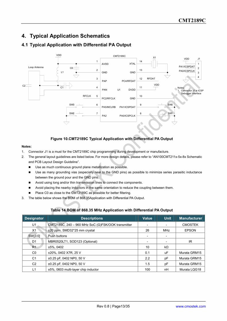
4. Typical Application Schematics
4.1 Typical Application with Differential PA Output
U1
XTALAVDD
GND GND
1
X1
PC4/RFDATPAP
CMT2189C
DVDDPAN
PC2/RFCLK GND
2
3
4
5
6
7
14
13
12
11
10
9
8
RFCLK
VDD
Loop Antenna
RFDAT
J1VDD
1
2
3
4
SW0
SW1SW2
SW3
C0
L1
C2 VDDC1
PA5/MCLRB
PA2 PA0/ICSPCLK
PA1/ICSPDAT
PA1/ICSPDAT
PA0/ICSPCLK
Notes:
1. Connector J1 is ICSP
Debugger Interface
Figure 10.CMT2189C Typical Application with Differential PA Output
Notes:
1. Connector J1 is a must for the CMT2189C chip programming during development or manufacture.
2. The general layout guidelines are listed below. For more design details, please refer to “AN100CMT211x-5x-8x Schematic
and PCB Layout Design Guideline”.
Use as much continuous ground plane metallization as possible.
Use as many grounding vias (especially near to the GND pins) as possible to minimize series parasitic inductance
between the ground pour and the GND pins.
Avoid using long and/or thin transmission lines to connect the components.
Avoid placing the nearby inductors in the same orientation to reduce the coupling between them.
Place C0 as close to the CMT2189C as possible for better filtering.
3. The table below shows the BOM of 868.35Application with Differential PA Output.
Table 14.BOM of 868.35 MHz Application with Differential PA Output
Designator Descriptions Value Unit Manufacturer
U1 CMT2189C, 240 – 960 MHz SoC (G)FSK/OOK transmitter - - CMOSTEK
X1 ±20 ppm, SMD32*25 mm crystal 26 MHz EPSON
SW[3:0] Push buttons - -
D1 MBR0520LT1, SOD123 (Optional) - - IR
R1 ±5%, 0402 10 kΩ
C0 ±20%, 0402 X7R, 25 V 0.1 uF Murata GRM15
C1 ±0.25 pF, 0402 NP0, 50 V 2.2 pF Murata GRM15
C2 ±0.25 pF, 0402 NP0, 50 V 1.5 pF Murata GRM15
L1 ±5%, 0603 multi-layer chip inductor 100 nH Murata LQG18

CMT2189C
Rev 0.8 | Page14/35 www.cmostek.com
4.2 Typical Application with Single-ended PA Output
U1
1
X1CMT2189C
2
3
4
5
6
7
14
13
10
9
8
CLK
VDD
VTG
CLK2
DATA2 SW0
SW1SW2
SW3
C0
L1
L2
C2
C1
ANT
L3
C3
12
11
DATA
VDD
AVDD
GND
PAP
PAN
PC2/RFCLK
PA5/MCLRB
PA2
J1VDD
1
2
3
4
PA1/ICSPDAT
PA0/ICSPCLK
XTAL
GND
PC4/RFDAT
DVDD
GND
PA0/ICSPCLK
PA1/ICSPDAT
Notes:
1. Connector J1 is ICSP
Debugger Interface
Figure 11. CMT2189C Typical Application with Single-ended PA Output
Notes:
1. Connector J1 is a must for the CMT2189C chip programming during development or manufacture.
2. The general layout guidelines are listed below. For more design details, please refer to “AN100CMT211x-5x-8x Schematic
and PCB Layout Design Guideline”.
Use as much continuous ground plane metallization as possible.
Use as many grounding vias (especially near to the GND pins) as possible to minimize series parasitic inductance
between the ground pour and the GND pins.
Avoid using long and/or thin transmission lines to connect the components.
Avoid placing the nearby inductors in the same orientation to reduce the coupling between them.
Place C0 as close to the CMT2189C as possible for better filtering.
3. The table below shows the BOM of868.35 Application with single-ended PA output.
Table15. BOM of868.35 MHz FCC/ETSI Compliant Application
Designator Descriptions Value Unit Manufacturer
U1 CMT2189C, 240 – 960 MHz SoC(G)FSK/OOK transmitter - - CMOSTEK
X1 ±20 ppm, SMD32*25 mm crystal 26 MHz EPSON
SW[3:0] Push buttons - -
D1 MBR0520LT1, SOD123 (Optional) - - IR
R1 ±5%, 0402 10 kΩ
C0 ±20%, 0402 X7R, 25V 0.1 uF Murata GRM15
C1 ±5%, 0402 NP0, 50V 68 pF Murata GRM15
C2 ±5%, 0402 NP0, 50V 9.1 pF Murata GRM15
C3 ±5%, 0402 NP0, 50V 8.2 pF Murata GRM15
L1 ±5%, 0603 multi-layerchip inductor 100 nH MurataLQG18
L2 ±5%,0603 multi-layerchip inductor 8.2 nH MurataLQG18
L3 ±5%,0603 multi-layerchip inductor 8.2 nH MurataLQG18

CMT2189C
Rev 0.8 | Page15/35 www.cmostek.com
5. Functional Descriptions
LDOs
PFD/CP
Fractional -N
DIV
Interface and Digital Logic
EEPROM
Loop Filter
ModulatorRamp
Control
VCOXOSC
AVDD GNDXTAL
RFCLKRFDAT
PAP
POR Bandgap
PA
CPU
Program Flash
2048 * 14 Bits
Data EEPROM
256 * 8 Bits
TMR/WDT
IO
CMP
RSTC/OST/
PWRT/BOOT
CLKC
(IRCCK)
SFR
SRAM
128 * 8 Bits
CFG
DVDD
PA0 PA1 PA2 PA5 PC4 PC2
TWI
PAN
Figure 12. CMT2189C Functional Block Diagram
5.1 Overview
The CMT2189C devices are fully integrated, highly flexible, high performance, SoC (G)FSK/OOK transmitters with an
embedded RISC microcontroller designed for various 240 to 960 MHz wireless applications. They are part of the CMOSTEK
NextGenRFTM family, which includes a complete line of transmitters, receivers and transceivers. The chip is optimized for the
low system cost, low power consumption, battery powered application with its highly integrated and low power design.
The functional block diagram of the CMT2189C is shown in the figure above. The CMT2189C is based on direct synthesis of
the RF frequency, and the frequency is generated by a low-noise fractional-N frequency synthesizer. It uses a 1-pin crystal
oscillator circuit with the required crystal load capacitance integrated on-chip to minimize the number of external components.
Every analog block is calibrated on each Power-on Reset (POR) to the reference voltage generated by Bandgap. The
calibration can help the chip to finely work under different temperatures and supply voltages. The CMT2189C has a highly
efficient PA built in, the PA can be configured as single-ended or differential outputs, and the output power can be configured
from -10 to +13 dBm in 1 dB step size. The RISC microcontroller has2048-word flash program space. Up to 4 I/O are
supported with their functions customized by the user program. RF Frequency, PA output power, other product features and
unique transmit IDs can be programmed into the embedded EEPROM. This saves the cost and simplifies the product
development and manufacturing effort. Alternatively, in stock products of 868.35 MHz is available for immediate demands. The
CMT2189C operates from 2.0 to 3.6 V, only consumes 12.4 mA when transmitting +10 dBm power under 3.3 V supply voltage.
The device together with CMOSTEK NextGenRFTM receiver enables a highly flexible, low cost RF link.
5.2 Modulation, Frequency, Deviation and Symbol Rate
The CMT2189C supports OOK modulation with the symbol rate up to 30 ksps, as well as the (G)FSK modulation with the
symbol rate up to 100 ksps. The supported deviation frequency is from 1 kHz to 200 kHz. The CMT2189C continuously covers
the frequency range from 240 to 960 MHz, including the license free ISM frequency band around 315 MHz433.92 MHz, 868.35
MHz and915 MHz. The device contains a high spectrum purity low power fractional-N frequency synthesizer with output
frequency resolution better than 198 Hz when the RF frequency is lower than 480 MHz, and is 397 Hz when the RF frequency
is higher than 480 MHz, see the table below for the modulation, frequency, Deviation and symbol rate specifications.

CMT2189C
Rev 0.8 | Page16/35 www.cmostek.com
Table 16. Modulation, Frequency, Deviation and Symbol Rate
Parameter Value Unit
Modulation (G)FSK/OOK -
Frequency 240 to960 MHz
Deviation 1 to 200 kHz
Frequency Resolution (FRF≤ 480 MHz) <198 Hz
Frequency Resolution (FRF> 480 MHz) 397 Hz
(G)FSK Symbol Rate 0.5 to100 ksps
OOK Symbol Rate 0.5 to30 ksps
5.3 Power Amplifier
A highly efficient Power Amplifier (PA) is integrated in the CMT2189C to transmit the modulated signal out. Depending on the
application, the PA can be configured as single-ended or differential output on the RFPDK, and the user can design a matching
network for the PA to exhibit optimum efficiency at the desired output power for a wide range of antennas, such as loop or
monopole antenna. Typical application schematics and the required BOM are shown in “Chapter 4 Typical Application
Schematic”. For the schematic, layout guideline and the other detailed information please refer to “AN100CMT211x-5x-8x
Schematic and PCB Layout Design Guideline”.
The output power of the PA can be configured by the user within the range from -10 dBm to +13 dBm in 1 dB step size using
the CMOSTEK USB Programmer and the RFPDK(just as CMT2119A), and also can be configured by software using the TWI.
5.4 PA Ramping
When the PA is switched on or off quickly, its changing input impedance momentarily disturbs the VCO output frequency. This
process is called VCO pulling, and it manifests as spectral splatter or spurs in the output spectrum around the desired carrier
frequency. By gradually ramping the PA on and off, PA transient spurs are minimized. The CMT2189C has built-in PA ramping
configurability with options of 0, 1, 2, 4, 8, 16, 32, 64, 128, 256, 512 and 1024 us, as shown in Figure. When the option is set to
“0”, the PA output power will ramp up to its configured value in the shortest possible time. The ramp down time is identical to
the ramp up time in the same configuration.
CMOSTEK recommends that the maximum symbol rate should be no higher than 1/2 of the PA ramping “rate”, as shown in the
formula below.
SRMax ≤ 0.5 * (1
tRAMP
)
In which the PA ramping “rate” is given by (1/tRAMP). In other words, by knowing the maximum symbol rate in the application,
the PA ramping time can be calculated by formula below.
tRAMP ≤ 0.5 * (1
SRMAX
)
The user can select one of the values of the tRAMP in the available options that meet the above requirement. If somehow the
tRAMP is set to be longer than “0.5 * (1/SRMax)”, it will possibly bring additional challenges to the OOK demodulation of the
Rxdevice. For more detail of calculating tRAMP, please refer to “AN132 CMT2180/89AConfiguration Guideline”.

CMT2189C
Rev 0.8 | Page17/35 www.cmostek.com
Time
RF
O A
mp
litu
de
Time
Da
ta
Logic 1 Logic 0
1024 us
512 us
8 us
4 us
2 us
1 us0 us
Figure 13. PA Ramping Time
5.5 Crystal Oscillator and RCLK
The CMT2189C uses a 1-pin crystal oscillator circuit with the required crystal load capacitance integrated on-chip. Figure 15
shows the configuration of the XTAL circuitry and the crystal model. The recommended specification for the crystal is 26 MHz
with ±20 ppm, ESR (Rm) < 60 Ω, load capacitance CLOAD ranging from 12 to 20 pF. To save the external load capacitors, a set
of variable load capacitors CL is built inside the CMT2189C to support the oscillation of the crystal.
The value of load capacitors is configurable with the CMOSTEK USB Programmer and RFPDK. To achieve the best
performance, the user only needs to input the desired value of the XTAL load capacitance CLOAD of the crystal (can be found in
the datasheet of the crystal) to the RFPDK, then finely tune the required XO load capacitance according to the actual XO
frequency.
CMT2189C
XTAL
Crystal Model
Rm
Cm CLC0
Lm
CMT2189C
XTAL
CL
RCLK
26 MHz
Cc
0. 3 – 0. 7 Vpp
If a 26 MHz RCLK (reference clock) is available in the system, the user can directly use it to drive the CMT2189C by feeding
the clock into the chip via the XTAL pin. This further saves the system cost due to the removal of the crystal. A coupling
capacitor is required if the RCLK is used. The recommended amplitude of the RCLK is 0.3 to 0.7 Vpp on the XTAL pin. Also,
the user should set the internal load capacitor CL to its minimum value. See Figure 14for the RCLK circuitry.
Figure 14.RCLK Circuitry
Figure 15.XTAL Circuitry and Crystal Model

CMT2189C
Rev 0.8 | Page18/35 www.cmostek.com
6. RFWorking States and Control Interface
6.1 Working States
The CMT2189C’s RF has following 4 different working states: SLEEP, XO-STARTUP, TUNE and TRANSMIT.
SLEEP
When the CMT2189C is in the SLEEP state, all the internal blocks are turned off and the current consumption is minimized.
XO-STARTUP
Once the modulator of the CMT2189C detect valid signal on the DRAW wire (see Figure 12), the RF section will go into the
XO-STARTUP state, and the internal XO starts to work. The user has to wait for the tXTAL to allow the XO to get stable. The tXTAL
is to a large degree crystal dependent. A typical value of tXTAL is provided in the Table .
TUNE
The frequency synthesizer will tune the CMT2189C to the desired frequency in the time tTUNE.The PA can be turned on to
transmit the data only after the TUNE state is done, before that the data will not be transmitted. See Figure 16 and Figure 17for
the details.
TRANSMIT
The CMT2189C starts to modulate and transmit the data (DRAW) generated by the microcontroller core responding to the push
buttons. The transmission can be ended in 2 methods: firstly, driving the DATA pin low for tSTOP time, where the tSTOP can be
configured from 20 to 90 ms on the RFPDK; secondly, issuing SOFT_RST command over the two-wire interface, this will stop
the transmission in 1 ms. See section 6.2.3for details of the two-wire interface.
Table 17.Timing in Different Working States
Parameter Symbol Min Typ Max Unit
XTAL Startup Time [1] tXTAL 400
us
Time to Tune to Desired Frequency tTUNE 370 us
Hold Time After Rising Edge tHOLD 10 ns
Time to Stop The Transmission[2] tSTOP 2 90 ms
Notes:
[1]. This parameter is to a large degree crystal dependent.
[2]. Configurable from 2 to 9 in 1 ms step size and 20 to 90 ms in 10 ms step size.
6.2 Transmission Control Interface
The CMT2189C uses the DRAW wire for the microcontroller core to send in data for modulation and transmission. The DRAW wire,
which also connects to the DATA pin, can be used as pin for EEPROM programming, data transmission, as well as controlling
the transmission. The transmission can be started by detecting rising or falling edge on the DRAW wire (DATA Pin), and stopped
by driving the DRAW wire low for tSTOP as shown in the table above. Besides communicating over the DRAW wire, the
microcontroller core can also communicate with the RF section over the two-wire interface, so that the transmission is more
robust, and consumes less current.
Please note that the user is recommended to use the Tx Enabled by DATA pin Rising Edge, which is described in Section
6.2.1.

CMT2189C
Rev 0.8 | Page19/35 www.cmostek.com
6.2.1 Tx Enabled by DATA Pin Falling Edge
As shown in the figure below, once the CMT2189C detects a falling edge on the DRAW wire (can be observed on DATA pin), it
goes into XO-STARTUP state and the XO starts to work. During the XO-STARTUP state, the DRAW wire needs to be pulled low.
After the XO is settled, the CMT2189C goes to the TUNE state. The logic state of the DRAW wire is “Don’t Care” during the
TUNE state. In the TRANSMIT state, PA sends out the data generated by the microcontroller core after they are modulated.
The user has to pull the DRAW wire low for tSTOP in order to end the transmission. Before starting the next transmit cycle, the
user has to pull the DRAW wire back to high.
PA out
SLEEPSLEEPSTATE
RF Signals
tXTAL
TUNE
tTUNE
DRAW wire
(DATA pin)1 0 Don’t Care Valid Transmitted Data 0 1
tSTOP
TRANSMITXO-STARTUP
Falling Edge
Figure 16. Transmission Enabled by DATA Pin Falling Edge
6.2.2 Tx Enabled by DATA Pin Rising Edge
As shown in the figure below, once the CMT2189C detects a rising edge on the DRAW wire(DATA pin), it goes into the
XO-STARTUP state. The user has to pull the DRAW wire high for at least 10 ns (tHOLD) after detecting the rising edge, as well as
wait for the sum of tXTAL and tTUNE before sending any useful information (data to be transmitted) into the chip on the DRAW wire.
The logic state of the DRAW wire is “Don’t Care” from the end of tHOLD till the end of tTUNE. In the TRANSMIT state, PA sends out
the input data after they are modulated. The user has to pull the DRAW wire low for tSTOP in order to end the transmission.
SLEEPSLEEP TRANSMITSTATE
PA out RF Signals
tSTOPtXTAL
TUNEXO-STARTUP
tTUNE
Valid Transmitted DataDon’t Care0 1
tHOLD
0
Rising Edge
DRAW wire
(DATA pin)
Figure 17. Transmission Enabled by DATA Pin Rising Edge
6.2.3 Two-wire Interface(TWI)
For power-saving and reliable transmission purposes, the CMT2189C is recommended to communicate with the
microcontroller core over a two-wire interface (TWI): DRAW (DATA) and CLK. The TWI is designed to operate at a maximum of 1
MHz. The timing requirement and data transmission control through the TWI are shown in this section.
CMT2189C
Rev 0.8 | Page20/35 www.cmostek.com
Table 18.TWI Requirements
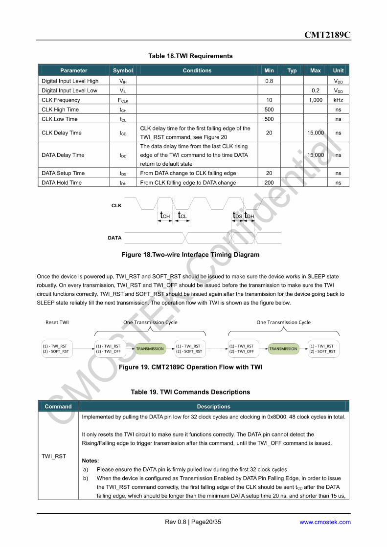
Parameter Symbol Conditions Min Typ Max Unit
Digital Input Level High VIH 0.8 VDD
Digital Input Level Low VIL 0.2 VDD
CLK Frequency FCLK 10 1,000 kHz
CLK High Time tCH 500 ns
CLK Low Time tCL 500 ns
CLK Delay Time tCD CLK delay time for the first falling edge of the
TWI_RST command, see Figure 20 20 15,000 ns
DATA Delay Time tDD
The data delay time from the last CLK rising
edge of the TWI command to the time DATA
return to default state
15,000 ns
DATA Setup Time tDS From DATA change to CLK falling edge 20 ns
DATA Hold Time tDH From CLK falling edge to DATA change 200 ns
tDS tDHtCH tCL
CLK
DATA
Figure 18.Two-wire Interface Timing Diagram
Once the device is powered up, TWI_RST and SOFT_RST should be issued to make sure the device works in SLEEP state
robustly. On every transmission, TWI_RST and TWI_OFF should be issued before the transmission to make sure the TWI
circuit functions correctly. TWI_RST and SOFT_RST should be issued again after the transmission for the device going back to
SLEEP state reliably till the next transmission. The operation flow with TWI is shown as the figure below.
One Transmission Cycle
(1) - TWI_RST(2) - SOFT_RST
(1) - TWI_RST(2) - TWI_OFF
(1) - TWI_RST(2) - SOFT_RST
TRANSMISSION
Reset TWI One Transmission Cycle
(1) - TWI_RST(2) - TWI_OFF
(1) - TWI_RST(2) - SOFT_RST
TRANSMISSION
Figure 19. CMT2189C Operation Flow with TWI
Table 19. TWI Commands Descriptions
Command Descriptions
TWI_RST
Implemented by pulling the DATA pin low for 32 clock cycles and clocking in 0x8D00, 48 clock cycles in total.
It only resets the TWI circuit to make sure it functions correctly. The DATA pin cannot detect the
Rising/Falling edge to trigger transmission after this command, until the TWI_OFF command is issued.
Notes:
a) Please ensure the DATA pin is firmly pulled low during the first 32 clock cycles.
b) When the device is configured as Transmission Enabled by DATA Pin Falling Edge, in order to issue
the TWI_RST command correctly, the first falling edge of the CLK should be sent tCD after the DATA
falling edge, which should be longer than the minimum DATA setup time 20 ns, and shorter than 15 us,

CMT2189C
Rev 0.8 | Page21/35 www.cmostek.com
Command Descriptions
as shown in Figure 20.
c) When the device is configured as Transmission Enabled by DATA Pin Rising Edge, the default state of
the DATA is low, there is no tCD requirement, as shown in Figure 21.
TWI_OFF
Implemented by clocking in 0x8D02, 16 clock cycles in total.
It turns off the TWI circuit, and the DATA pin is able to detect the Rising/Falling edge to trigger transmission
after this command, till the TWI_RST command is issued. The command is shown as Figure 22.
SOFT_RST
Implemented by clocking in 0xBD01, 16 clock cycles in total.
It resets all the other circuits of the chip except the TWI circuit. This command will trigger internal calibration
for getting the optimal device performance. After issuing the SOFT_RST command, the host MCU should
wait 1 ms before sending in any new command. After that, the device goes to SLEEP state. The command is
shown as Figure 23.
CLK
32 clock cycles
… …
16 clock cycles
DATA
tCD
01
tDD
10x8D00
Figure 20. TWI_RST Command When Transmission Enabled by DATA Pin Falling Edge
CLK
32 clock cycles
… …
16 clock cycles
DATA 0x8D000 0
Figure 21. TWI_RST Command When Transmission Enabled by DATA Pin Rising Edge
DATA
CLK
16 clock cycles
0x8D02 (TWI_OFF)
… tDD
Default State DATA
CLK
16 clock cycles
0xBD01 (SOFT_RST)
… tDD
Default State
The DATA is generated by the host MCU on the rising edge of CLK, and is sampled by the device on the falling edge. The CLK
should be pulled up by the host MCU during the TRANSMISSION shown in Figure 19. The TRANSMISSION process should
refer to Figure 16 or Figure 17 for its timing requirement, depending on the “Start By” setting configured on the RFPDK.
The device will go to SLEEP state by driving the DATA low for tSTOP, or issuing SOFT_RST command. A helpful practice for the
device to go to SLEEP is to issue TWI_RST and SOFT_RST commands right after the useful data is transmitted, instead of
waiting the tSTOP, this can save power significantly.
Figure 22. TWI_OFF Command Figure 23. SOFT_RST Command

CMT2189C
Rev 0.8 | Page22/35 www.cmostek.com
7. RISC Microcontroller Core
The embedded high-performance RISC Microcontroller has the following features:
Program Counter
8-Level Stack
(13-bit)
RAM File
Registers
128 x 8
Flash
Program
Memory
2k x 14
Instruction Reg
Internal
32 kHz-16 MHz
Oscillator
Instruction
Decode &
Control
Timing
Generation
Power-on
Reset
Watchdog
Timer
Power-down
Reset
Addr MUX
FSR Reg
STATUS Reg
MUX
W Reg
Timer 2Timer 0
PA0
PA1
PA2
PA5/MCLRB
PC2/RFCLK
PC4/RFDAT
8Data Bus13
RAM Addr
Indirect
AddrDirect Addr
14Program
Bus
VDD/GND
ALU
T0CKI
Figure 24.Microcontroller Core Block Diagram
High-Performance RISC CPU
- 2048 words Flash ROM, 128B SRAM
- 256B EEPROM
- All single-cycle instructions except branches
- Operating Speed
DC - 16MHz oscillator
125 ns instruction cycle
- Interrupt Capability
- 8-Level Deep Hardware Stack
- Power-Saving Sleep mode
- Power-on Reset (POR)
- Multiplexed MCLRB/Input Pin
Peripheral Features
- 4 I/O Pins
Individual Direction Control
Interrupt-on-Pin Change
Individual Programmable Weak Pull-ups
- Timer0: 8-bit timer with 3-bit prescaler
- Timer2: 8-bit timer with 3-bit prescaler
- Watchdog timer with on-chip RC oscillator
CMT2189C
Rev 0.8 | Page23/35 www.cmostek.com
7.1 Memory Organization
7.1.1 Program Memory Organization
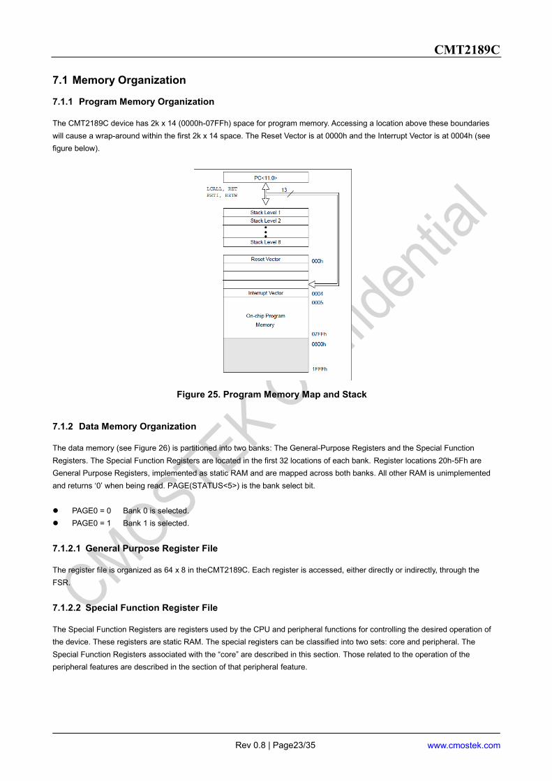
The CMT2189C device has 2k x 14 (0000h-07FFh) space for program memory. Accessing a location above these boundaries
will cause a wrap-around within the first 2k x 14 space. The Reset Vector is at 0000h and the Interrupt Vector is at 0004h (see
figure below).
Figure 25. Program Memory Map and Stack
7.1.2 Data Memory Organization
The data memory (see Figure 26) is partitioned into two banks: The General-Purpose Registers and the Special Function
Registers. The Special Function Registers are located in the first 32 locations of each bank. Register locations 20h-5Fh are
General Purpose Registers, implemented as static RAM and are mapped across both banks. All other RAM is unimplemented
and returns ‘0’ when being read. PAGE(STATUS<5>) is the bank select bit.
PAGE0 = 0 Bank 0 is selected.
PAGE0 = 1 Bank 1 is selected.
7.1.2.1 General Purpose Register File
The register file is organized as 64 x 8 in theCMT2189C. Each register is accessed, either directly or indirectly, through the
FSR.
7.1.2.2 Special Function Register File
The Special Function Registers are registers used by the CPU and peripheral functions for controlling the desired operation of
the device. These registers are static RAM. The special registers can be classified into two sets: core and peripheral. The
Special Function Registers associated with the “core” are described in this section. Those related to the operation of the
peripheral features are described in the section of that peripheral feature.

CMT2189C
Rev 0.8 | Page24/35 www.cmostek.com
Figure 26. Data Memory Map of the CMT2189C

CMT2189C
Rev 0.8 | Page25/35 www.cmostek.com
Table 20. CMT2189C Special Registers Summary Bank0
ADDR Name Bit7 Bit6 Bit5 Bit4 Bit3 Bit2 Bit1 Bit0 POR reset
0 INDF Addressing this location uses contents of FSR to address data memory (not a physical register) x x x x x x x x
1 TMR0 Timer0 Module’s register, Timer0<7:0> x x x x x x x x
2 PCL Program Counter’s (PC) Least Significant Byte, PC<7:0> 0000 0000
3 STATUS - - PAGE /TF /PF Z HC C - - 0 1 1 x x x
4 FSR Indirect Data Memory Address Pointer
5 PORTA PA7 PA6 PA5 PA4 PA3 PA2 PA1 PA0 00x0 0000
6 - - - - - - - -
7 PORTC PC7 PC6 PC5 PC4 PC3 PC2 PC1 PC0 0000 0000
8 - - - - - - - -
9 - - - - - - - -
A PCLATH - - - Write Buffer for upper 5 bits of Program Counter, PC<13:8> - - - 0 0 0 0 0
B INTCON GIE PEIE T0IE INTE PAIE T0IF INTF PAIF 0000 0000
C PIR1 EEIF CKMEAIF - C2IF C1IF OSFIF TMR2IF - 0 0 - 0 00 0-
D - - - - - - - -
E - - - - - - - -
F - - - - - - - -
10 - - - - - - - -
11 TMR2 Timer2 Module register, Timer2<7:0> 0000 0000
12 T2CON - TOUTPS<3:0> TMR2ON T2CKPS<1:0> -000 0000
13 - - - - - - - -
14 - - - - - - - -
15 - - - - - - - -
16 - - - - - - - -
17 - - - - - - - -
18 WDTCON - - - WDTPS<3:0> SWDTEN - - - 0 1 0 0 0
19 CMCON0 C2OUT C1OUT C2INV C1INV CIS CM<2:0> 0000 0000
1A PR0 PR0<7:0> 1111 1111
1B MSCKCON - - - SLVREN - CKMAVG CKCNTI - - - - 0 - 0 0 -
1C SOSCPPRL SOSCPR<7:0> 1111 1111
1D SOSCPRH - - - - SOSCPR<11:8> - - - - 1 1 1 1
1E - - - - - - - -
1F - - - - - - - -

CMT2189C
Rev 0.8 | Page26/35 www.cmostek.com
Table 21. CMT2189C Special Function Registers Summary Bank1
ADDR Name Bit7 Bit6 Bit5 Bit4 Bit3 Bit2 Bit1 Bit0 POR reset
80 INDF Addressing this location uses contents of FSR to address data memory (not a physical register) x x x x x x x x
81 OPTION /PAPU INTEDG T0CS T0SE PSA PS2 PS1 PS0 1111 1111
82 PCL Program Counter’s (PC) Least Significant Byte, PC<7:0> 0000 0000
83 STATUS - - PAGE /TF /PF Z HC C - - 0 1 1 x x x
84 FSR Indirect Data Memory Address Pointer
85 TRISA TRISA<7:6> -- TRISA<4:0> 11x1 1111
86 - - - - - - - -
87 TRISC TRISC<7:0> 1111 1111
88 - - - - - - - -
89 - - - - - - - -
8A PCLATH - - - Write Buffer for upper 5 bits of Program Counter, PC<13:8> - - - 0 0 0 0 0
8B INTCON GIE PEIE T0IE INTE PAIE T0IF INTF PAIF 0000 0000
8C PIE1 EEIE CKMEAIE - C2IE C1IE OSFIE TMR2IE - 0 0 - 0 0 0 0 -
8D - - - - - - - -
8E PCON /POR /BOR - - - - - - q q
8F OSCCON LFMOD IRCF[2:0] OSTS HTS LTS SCS 0101 x000
90 - - - - - - - -
91 0000 0000
92 PR2 PR2[7:0], Timer2 period register 1111 1111
93 - - - - - - - -
94 - - - - - - - -
95 WPUA WPUA<7:6> - WPUA<4:0> 1 1-1 11 1 1
96 IOCA IOCA<7:0> - - - - - - - -
97 - - - - - - - -
98 - - - - - - - -
99 VRCON VREN - VRR - VR<3:0> 0 - 0 - 0 0 0 0
9A EEDAT EEDAT<7:0> 0000 0000
9B EEADR EEADR<7:0> 0000 0000
9C EECON1 - - WREN3 WREN2 WRERR WREN1 - RD - - 0 0 x 0 - 0
9D EECON2 - - - - - - - WR - - - - - - - 0
9E - - - - - - - -
9F - - - - - - - -
7.2 Port A
There have four general purpose I/O pins available, PA0~PA2, and PA5, as shown in the table below. Depending on which
peripherals are enabled, some or all of the pins may not be available as general purpose I/O. In general, when a peripheral is
enabled, the associated pin may not be used as a general purpose I/O pin.

CMT2189C
Rev 0.8 | Page27/35 www.cmostek.com
Table 22. Mapping from the GPIOs to the Pinouts
GPIO Pinout
PA0 PA0/ICSPCLK
PA1 PA1/ICSPDAT
PA2 PA2
PA5 PA5/MCLRB
7.2.1 PORTA and the CPIOA Registers
PORTA is a 6-bit wide, bidirectional port. The corresponding data direction register is TRISA. Setting a TRISA bit (= 1) will
make the corresponding PORTA pin as input (i.e., put the corresponding output driver in a High-Impedance mode). Clearing a
TRISA bit (= 0) will make the corresponding PORTA pin as output (i.e., put the contents of the output latch on the selected pin).
The exception is PA5, which is input only and its TRISA bit will always read as ‘1’.
Reading the PORTA register reads the status of the pins, whereas writing to it will write to the PORT latch. All write operations
are read-modify-write operations. Therefore, a write to a port implies that the port pins are read; this value is modified and then
written to the PORT data latch. PA5 reads ‘0’ when MCLRE = 1.
7.2.2 Additional Pin Functions
Every PORTA pin on the CMT2189C has an interrupt-on-change(IOC) option and every PORTA pin has a pull-up option.
7.2.2.1 Pull-up
Each of the PORTA pinshas an individually configurable internal pull-up. Control bits WPUA enable or disable each pull-up.
7.2.2.2 Interrupt-On-Change
Each of the PORTA pins is individually configurable as an interrupt-on-change pin. Control bits IOCA enable or disable the
interrupt function for each pin. The interrupt-on-change is disabled on a Power-on Reset. For enabled interrupt-on-change pins,
the values are compared with the old value latched on the last read of PORTA. The ‘mismatch’ outputs of the last read are
OR’d together to set, the PORTA Change Interrupt Flag bit (PAIF) in the INTCON register. This interrupt can wake the device
from Sleep. The user, in the Interrupt Service Routine, can clear the interrupt by:
1) Any read or write of PORTA. This will end the mismatch condition, then.
2) Clear the flag bit PAIF.
A mismatch condition will continue to set flag bit PAIF. Reading PORTA will end the mismatch condition and allow flag bit PAIF
to be cleared. The latch holding the last read value is not affected by a MCLR nor BOD Reset. After these resets, the PAIF flag
will continue to be set if a mismatch is present.
7.3 PORTC
PORTC is a general purpose I/O port consisting of 6bidirectional pins. The pins can be configured for either digital I/O, but only
PC2 and PC4 has been pin out. PC2 is connected to the TWI’s CLK, and PC4 is connected to the TWI’s DAT. Both are used to
configuration the RF parameters.
CMT2189C
Rev 0.8 | Page28/35 www.cmostek.com
Table 23. Mapping from the TWI to the Pinouts
GPIO RF Part
PC2 CLK
PC4 DAT
7.4 Timer0 Module
The Timer0 module timer/counter has the following features.
• 8-bit timer/counter
• Readable and writable
• 8-bit software programmable prescaler
• Internal or external clock select
• Interrupt on overflow from FFh to 00h
• Edge select for external clock
Figure 27is a block diagram of the Timer0 module and the prescaler shared with the WDT.
Figure 27. Block Diagram of the Timer0/WDT Prescaler
7.4.1 Timer0 Operation
Timer mode is selected by clearing the T0CS bit(OPTION<5>). In Timer mode, the Timer0module will increment every
instruction cycle (without prescaler). If TMR0 is written, the increment is in habited for the following two instruction cycles. The
user can work around this by writing an adjusted value to theTMR0 register.
Counter mode is selected by setting the T0CS bit(OPTION<5>). In this mode, the Timer0 module will increment either on every
rising or falling edge of pin PA2/T0CKI. The incrementing edge is determined by the source edge (T0CE) control
bit(OPTION<4>). Clearing the T0CE bit selects the rising edge.
7.4.2 Timer0 Interrupt
A Timer0 interrupt is generated when the TMR0register timer/counter overflows from FFh to 00h. This overflow sets the T0IF
bit. The interrupt can be masked by clearing the T0IE bit (INTCON<5>). The T0IF bit(INTCON<2>) must be cleared in software

CMT2189C
Rev 0.8 | Page29/35 www.cmostek.com
by theTimer0 module Interrupt Service Routine before re-enabling this interrupt. The Timer0 interrupt can not wake the
processor from Sleep, since the timer is shutoff during Sleep.
7.4.3 Using Timer0 with an External Clock
When no prescaler is used, the external clock input is the same as the prescaler output. The synchronization of T0CKI, with
the internal phase clocks, is accomplished by sampling the prescaler output on the Q2 andQ4 cycles of the internal phase
clocks. Therefore, it is necessary for T0CKI to be high for at least 2TOSC(and a small RC delay of 20 ns) and low for at least
2TOSC(and a small RC delay of 20 ns). Refer to the electrical specification of the desired device.
7.4.4 Prescaler
An 8-bit counter is available as a prescaler for theTimer0 module, or as a postscaler for the Watchdog Timer. For simplicity,
this counter will be referred to as “prescaler” throughout this Datasheet. The prescaler assignment is controlled in software by
the control bit PSA (OPTION<3>). Clearing the PSA bit will assign the prescaler to Timer0. Prescale values are selectable via
the PS2:PS0 bits (OPTION<2:0>). The prescaler is not readable or writable. When assigned to the Timer0 module, all
instructions writing to the TMR0 register (e.g., CLRR 1, STWR 1,BSR 1, x....etc.) will clear the prescaler. When assigned to
WDT, a CLRWDT instruction will clear the prescaler along with the Watchdog Timer.
7.5 Timer2 Module
Figure 28shows the basic block diagram of the Timer2 module.
Figure 28. Timer2 Block Diagram

CMT2189C
Rev 0.8 | Page30/35 www.cmostek.com
8. Ordering Information
Table 24. CMT2189C Ordering Information
Part Number
Descriptions Package
Type
Package
Option
Operating
Condition
MOQ /
Multiple
CMT2189C-ESR[1] 240 – 960 MHz SoC
(G)FSK/OOK Transmitter SOP14 Tape & Reel
2.0 to 3.6 V,
-40 to 85 ℃ 2,500
CMT2189C-ESB[1] 240 – 960 MHz SoC
(G)FSK/OOK Transmitter SOP14 Tube
2.0 to 3.6 V,
-40 to 85 ℃ 1,000
Notes:
[1]. “E” stands for extended industrial product grade, which supports the temperature range from -40 to +85 ℃.
“S” stands for the package type of SOP14.
“R” stands for the tape and reel package option, the minimum order quantity (MOQ) for this option is 2,500 pcs. “B”
stands for the tube package option, with the MOQ of 1,000 pcs.
Visit www.cmostek.com/products to know more about the product and product line.
Contact [email protected] or your local sales representatives for more information.

CMT2189C
Rev 0.8 | Page31/35 www.cmostek.com
9. Package Outline
cθ
h
0.25
L
L1
A1
A3A2 A
D
b e
E1 E
Figure 29.14-Pin SOP Package
Table 25.14-Pin SOP Package Dimensions
Symbol Size (millimeters)
Min Typ Max
A - - 1.75
A1 0.05 - 0.225
A2 1.30 1.40 1.50
A3 0.60 0.65 0.70
b 0.39 - 0.48
C 0.21 - 0.26
D 8.45 8.65 8.85
E 5.80 6.00 6.20
E1 3.70 3.90 4.10
e 1.27 BSC
h 0.25 - 0.50
L 0.30 - 0.60
L1 1.05 BSC
θ 0 - 8°
CMT2189C
Rev 0.8 | Page32/35 www.cmostek.com
10. Top Marking
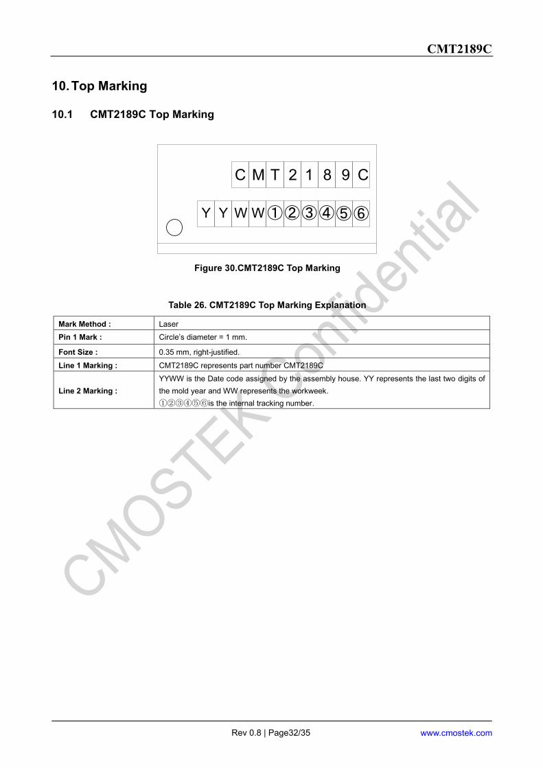
10.1 CMT2189C Top Marking
C M T 2 1 8 9 C
Y Y W W①②③④⑤⑥
Figure 30.CMT2189C Top Marking
Table 26. CMT2189C Top Marking Explanation
Mark Method : Laser
Pin 1 Mark : Circle’s diameter = 1 mm.
Font Size : 0.35 mm, right-justified.
Line 1 Marking : CMT2189C represents part number CMT2189C
Line 2 Marking :
YYWW is the Date code assigned by the assembly house. YY represents the last two digits of
the mold year and WW represents the workweek.
①②③④⑤⑥is the internal tracking number.

CMT2189C
Rev 0.8 | Page33/35 www.cmostek.com
11. Other Documentations
Table 27. Other Documentations for CMT2189C
Brief Name Descriptions
AN100 CMT211x-5x-8x Schematic and PCB
Layout Design Guideline(CN)
Details of CMT211x, CMT215x & CMT218x PCB schematic
and layout design rules, RF matching network and other
application layout design related issues.
AN132 CMT2180/89AConfiguration Guideline(EN) Details of configuring CMT2180/89A features on the RFPDK.
AN202 CMT2189C User Guide(CN) Details of using the CMT2189C

CMT2189C
Rev 0.8 | Page34/35 www.cmostek.com
12. Document Change List
Table 28. Document Change List
Rev. No. Chapter Description of Changes Date
0.8 All Initial Released 2018-1-1

CMT2189C
Rev 0.8 | Page35/35 www.cmostek.com
13. Contact Information
CMOSTEK Microelectronics Co., Ltd.
Room 202, Honghai Building, Qianhai Road. Nanshan District
Shenzhen, Guangdong, China PRC
Zip Code: 518000
Tel: 0755- 83235017
Fax: 0755- 82761326
Sales: [email protected]
Technical support: [email protected]
www.cmostek.com
The information furnished by CMOSTEK is believed to be accurate and reliable. However, no responsibility is assumed for
inaccuracies and specifications within this document are subject to change without notice. The material contained herein is
the exclusive property of CMOSTEK and shall not be distributed, reproduced, or disclosed in whole or in part without prior
written permission of CMOSTEK. CMOSTEK products are not authorized for use as critical components in life support
devices or systems without express written approval of CMOSTEK. The CMOSTEK logo is a registered trademark of
CMOSTEK Microelectronics Co., Ltd. All other names are the property of their respective owners.
Copyright. CMOSTEK Microelectronics Co., Ltd. All rights are reserved.