Embed Size (px)
Citation preview

JOURNAL OF LIGHTWAVE TECHNOLOGY, VOL. 25, NO. 2, FEBRUARY 2007 597
A Critical Comparison of High-Speed VCSELCharacterization Techniques
Christopher J. O’Brien, Marian L. Majewski, and Aleksandar D. Rakic, Member, IEEE
Abstract—This paper critically compares, for the first time,common microwave and optical procedures used for the high-speed characterization of vertical-cavity surface-emitting lasers(VCSELs). The intrinsic small-signal modulation characteristicsof a VCSEL are measured, and the related rate equation pa-rameters are extracted. Observed trends show excellent agree-ment with theory. The modulation characteristics of the VCSELare determined by examining three different responses: relativeintensity noise, S21 response, and high-resolution optical spectra.The various experimental techniques yielded consistent results.The relative strengths and weaknesses of each measurement areinvestigated.
Index Terms—Relative intensity noise (RIN), relaxation reso-nance frequency, vertical-cavity surface-emitting laser (VCSEL).
I. INTRODUCTION
V ERTICAL-CAVITY surface-emitting lasers (VCSELs)have grown greatly in popularity and capability. Unlike
conventional edge-emitting devices, VCSELs are designed witha very short resonant cavity, which supports a single longitudi-nal mode; light is emitted perpendicularly to the plane of crystalgrowth, allowing the construction of 2-D transmitter arrays forhigh-bandwidth density applications [1]–[6]. VCSELs have lowthreshold currents and high efficiencies and can be tested on thewafer, thus minimizing manufacturing costs [7].
VCSELs are heavily employed in high-bandwidth commu-nications applications and are particularly attractive candidatesfor use in optical interconnects. The maximum rate of directmodulation is limited by the interplay between photons andelectrons, whose response can be characterized by a relaxationfrequency fr and a damping frequency Γd.
A general rule of thumb is that a directly modulated lasercan support a bit rate of up to 1.2 times its relaxation resonantfrequency [8]; however, the parasitics of device packaging andbonding can severely inhibit high-frequency VCSEL perfor-mance [9], [10]. VCSEL chip bonding introduces capacitancefrom the pads and resistance from the leads; it is typically mod-eled as a first-order resistance–capacitance circuit [11], [12].The parasitics associated with packaged devices are more se-vere and tend to be represented by more complex circuit models[13], [14], but they still act as low-pass filters. Any attempt tomeasure the intrinsic response of a VCSEL will have to accountfor the parasitic effects of the packaging and bonding, as well as
Manuscript received February 19, 2006; revised October 8, 2006.The authors are with the School of Information Technology and Electrical
Engineering, University of Queensland, Brisbane, Qld. 4072, Australia (e-mail:[email protected]; [email protected]; [email protected]).
Color versions of one or more of the figures in this paper are available onlineat http://ieeexplore.ieee.org.
Digital Object Identifier 10.1109/JLT.2006.889362
the associated frequency response of measurement equipmentand driving circuitry. This can be achieved through accuratecircuit modeling of the parasitics, intelligent signal processingto remove the effects numerically, or observation of phenomenarelated to the intrinsic device properties, which will be immuneto the parasitic effects.
In the work that follows, the high-speed characteristics ofa VCSEL are examined, and the related intrinsic parametersare extracted. Three different experimental techniques are em-ployed to measure these quantities and to compare the consis-tency of results between measurements, immunity to parasitics,ease of measurement, and miscellaneous factors, such as theavailability of equipment and speed of measurement.
The nature of a VCSEL’s small-signal modulation responseis investigated in Section II; experimental processes and resultsare presented in Section III. A discussion relating to the diffi-culties and capabilities of each measurement technique followsin Section IV. Finally, conclusions are presented in Section V.
II. SMALL-SIGNAL MODULATION RESPONSE
The intrinsic transient behavior of VCSELs can be describedby the following rate equations [15]:
dS(t)dt
=ΓgN(t) −N0
1 + εS(t)S(t) − S(t)
τp+
ΓβN(t)τn
(1)
dN(t)dt
=I(t)qVa
− gN(t) −N0
1 + εS(t)S(t) − N(t)
τn(2)
dφ(t)dt
=αΓg2
(N(t) −Nth) (3)
whereN(t) carrier density,S(t) photon density,φ(t) optical phase,I(t) drive current,q electron charge,Va volume of the active region,τn carrier lifetime,g gain slope constant,α linewidth enhancement factor,N0 carrier density at transparency,Nth carrier density at threshold,ε nonlinear gain compression coefficient,Γ optical confinement factor,τp photon lifetime,β percentage of spontaneous emission that contributes
to the lasing mode.
0733-8724/$25.00 © 2007 IEEE
598 JOURNAL OF LIGHTWAVE TECHNOLOGY, VOL. 25, NO. 2, FEBRUARY 2007
The optical output power P (t) is proportional to the photondensity S(t) and is given by
P (t) =Vaηhν
ΓτpS(t) (4)
where η is the differential quantum efficiency of the laser, his the Planck’s constant, and ν is the lasing frequency. Thephenomena described by these rate equations produce a second-order frequency response under small-signal modulation[8], [9], [15], i.e.,
H(f) =f2
r
f2r − f2 + jΓd
f2π
(5)
Γd =1
2τn+Kf2
r (6)
K =2π2(τp + τc) (7)
fr =D√P =
√2ΓgVahν
P (8)
where f is the modulation frequency; fr is the relaxationresonant frequency; and Γd is the damping frequency. Parame-ters τc = ε/g, D, and K (the familiar K-factor) are lumpedparameters describing the relationship between the relaxationresonant and damping frequencies with optical power P . Theserelationships indicate that a laser’s high-frequency responseimproves at high drive currents and that the resonant peak willflatten with increasing drive current.
III. EXPERIMENTAL PROCEDURES AND RESULTS
The high-speed characterization of VCSELs requires greatcare in the experimental design stages, precise implementationof procedures, and very accurate well-calibrated high-speedinstrumentation. As a result, frequency-related measurementsare very difficult to perform and often inconsistent [16]. A num-ber of techniques exist to measure the intrinsic high-frequencyVCSEL characteristics and extract the related parameters.These include
1) measurement of the relative intensity noise (RIN) [17],2) fitting the S21 response to (5) and eliminating the
response of other network elements [15],3) examination of the optical spectrum at extremely high
resolution to identify RF spectral artifacts [18]–[21],4) observation of intermodulation and harmonic distortion
effects [22], [23].
The first three of these techniques are performed on anAvalon 850SM LA VCSEL, which emits strongly in the funda-mental mode—only one significant transverse mode lases overthe operation range of the device.
A. RIN
Even with a noise-free current source, variations will bepresent in a VCSEL’s steady-state output, as caused by spon-taneous emission; these stochastic variations are referred to as
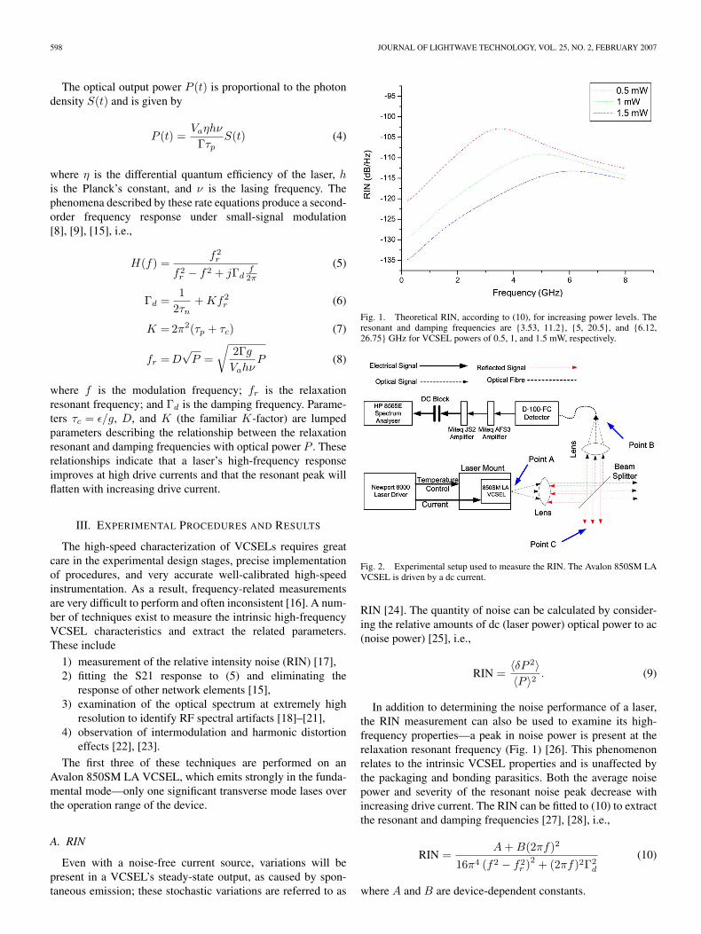
Fig. 1. Theoretical RIN, according to (10), for increasing power levels. Theresonant and damping frequencies are 3.53, 11.2, 5, 20.5, and 6.12,26.75 GHz for VCSEL powers of 0.5, 1, and 1.5 mW, respectively.
Fig. 2. Experimental setup used to measure the RIN. The Avalon 850SM LAVCSEL is driven by a dc current.
RIN [24]. The quantity of noise can be calculated by consider-ing the relative amounts of dc (laser power) optical power to ac(noise power) [25], i.e.,
RIN =〈δP 2〉〈P 〉2 . (9)
In addition to determining the noise performance of a laser,the RIN measurement can also be used to examine its high-frequency properties—a peak in noise power is present at therelaxation resonant frequency (Fig. 1) [26]. This phenomenonrelates to the intrinsic VCSEL properties and is unaffected bythe packaging and bonding parasitics. Both the average noisepower and severity of the resonant noise peak decrease withincreasing drive current. The RIN can be fitted to (10) to extractthe resonant and damping frequencies [27], [28], i.e.,
RIN =A+B(2πf)2
16π4 (f2 − f2r )2 + (2πf)2Γ2
d
(10)
where A and B are device-dependent constants.
O’BRIEN et al.: CRITICAL COMPARISON OF HIGH-SPEED VCSEL CHARACTERIZATION TECHNIQUES 599
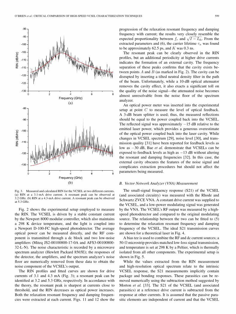
Fig. 3. Measured and calculated RIN for the VCSEL at two different currents.(a) RIN at a 3.1-mA drive current. A resonant peak can be observed at3.2 GHz. (b) RIN at a 4.3-mA drive current. A resonant peak can be observedat 5.3 GHz.
Fig. 2 shows the experimental setup employed to measurethe RIN. The VCSEL is driven by a stable constant currentby the Newport 8000 modular controller, which also maintainsa 298 K device temperature, and the light is coupled intoa Newport D-100-FC high-speed photodetector. The averageoptical power can be measured directly, and the RF com-ponent is transmitted through a dc block and two low-noiseamplifiers (Miteq JS2-00100800-17-0A and AFS3-00100800-32-L-N). The noise characteristic is recorded by a microwavespectrum analyzer (Hewlett Packard 8565E); the responses ofthe detector, the amplifiers, and the spectrum analyzer’s noisefloor are numerically removed from these data to obtain thenoise component of the VCSEL’s output.
The RIN profiles and fitted curves are shown for drivecurrents of 3.1 and 4.3 mA (Fig. 3); a resonant peak can beidentified at 3.2 and 5.3 GHz, respectively. In accordance withthe theory, the resonant peak is sharpest at currents close tothreshold, and the RIN decreases as optical power increases.Both the relaxation resonant frequency and damping frequen-cies were extracted at each current. Figs. 11 and 12 show the
progression of the relaxation resonant frequency and dampingfrequency with current; the results very closely resemble theexpected proportionality between fr and
√I − Ith. From the
extracted parameters and (6), the carrier lifetime τn was foundto be approximately 62.5 ps, and K was 0.3 ns.
The resonant peak can be clearly observed in the RINprofiles, but an additional periodicity at higher drive currentsindicates the formation of an external cavity. The frequencyseparation of these peaks confirms that the cavity exists be-tween points A and B (as marked in Fig. 2). The cavity can bedisrupted by inserting a tilted neutral density filter in the pathof the beam. Unfortunately, while a 10-dB optical attenuatorremoves the cavity effect, it also exacts a significant toll onthe quality of the noise signal—the attenuated noise becomesalmost unresolvable from the noise floor of the spectrumanalyzer.
An optical power meter was inserted into the experimentalsetup at point C to measure the level of optical feedback.A 3-dB beam splitter is used; thus, the measured reflectionsshould be equal to the power coupled back into the VCSEL.The reflected signal was approximately −15 dB relative to theemitted laser power, which provides a generous overestimateof the optical power coupled back into the laser cavity. Whilechanges in VCSEL spectrum [29], noise level [30], and trans-mission quality [31] have been reported for feedback levels aslow as −30 dB, Bae et al. demonstrate that VCSELs can beexposed to feedback levels as high as −13 dB without alteringthe resonant and damping frequencies [32]. In this case, theexternal cavity obscures the features of the noise signal andcomplicates extraction procedures but should not affect theparameters being measured.
B. Vector Network Analyzer (VNA) Measurement
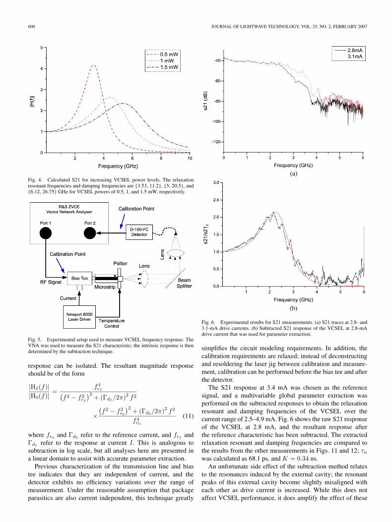
The small-signal frequency response (S21) of the VCSEL(and associated circuitry) was measured with the Rhode andSchwartz ZVCE VNA. A constant drive current was supplied tothe VCSEL, and a low-power modulating signal was generatedby the VNA. The VCSEL’s RF output was measured by a high-speed photodetector and compared to the original modulatingsource. The relationship between the two can be fitted to (5)to determine the relaxation resonant frequency and dampingfrequency of the VCSEL. The ideal S21 transmission curvesare shown for a theoretical laser in Fig. 4.
A bias tee is used to combine the RF and dc current sources; a50-Ω microstrip provides matched low-loss signal transmission,and temperature is set at 298 K by a Peltier, which is thermallyisolated from all other components. The experimental setup isshown in Fig. 5.
While the values extracted from the RIN measurementand high-resolution optical spectrum relate to the intrinsicVCSEL response, the S21 measurements implicitly containpackage and bonding responses. These parasitics can be re-moved numerically using the subtraction method suggested byMorton et al. [33]. The S21 of the VCSEL (and associatedparasitics) at a reference drive current is subtracted from theresponse at other currents. It is assumed that the passive para-sitic elements are independent of current and that the VCSEL
600 JOURNAL OF LIGHTWAVE TECHNOLOGY, VOL. 25, NO. 2, FEBRUARY 2007
Fig. 4. Calculated S21 for increasing VCSEL power levels. The relaxationresonant frequencies and damping frequencies are 3.53, 11.2, 5, 20.5, and6.12, 26.75 GHz for VCSEL powers of 0.5, 1, and 1.5 mW, respectively.
Fig. 5. Experimental setup used to measure VCSEL frequency response. TheVNA was used to measure the S21 characteristic; the intrinsic response is thendetermined by the subtraction technique.
response can be isolated. The resultant magnitude responseshould be of the form
|HI(f)||H0(f)| =
f4rI(
f2 − f2rI
)2 + (ΓdI/2π)2 f2
×(f2 − f2
r0
)2 + (Γd0/2π)2 f2
f4r0
(11)
where fr0 and Γd0 refer to the reference current, and frIand
ΓdIrefer to the response at current I . This is analogous to
subtraction in log scale, but all analyses here are presented ina linear domain to assist with accurate parameter extraction.
Previous characterization of the transmission line and biastee indicates that they are independent of current, and thedetector exhibits no efficiency variations over the range ofmeasurement. Under the reasonable assumption that packageparasitics are also current independent, this technique greatly
Fig. 6. Experimental results for S21 measurements. (a) S21 traces at 2.8- and3.1-mA drive currents. (b) Subtracted S21 response of the VCSEL at 2.8-mAdrive current that was used for parameter extraction.
simplifies the circuit modeling requirements. In addition, thecalibration requirements are relaxed; instead of deconstructingand resoldering the laser jig between calibration and measure-ment, calibration can be performed before the bias tee and afterthe detector.
The S21 response at 3.4 mA was chosen as the referencesignal, and a multivariable global parameter extraction wasperformed on the subtracted responses to obtain the relaxationresonant and damping frequencies of the VCSEL over thecurrent range of 2.5–4.9 mA. Fig. 6 shows the raw S21 responseof the VCSEL at 2.8 mA, and the resultant response afterthe reference characteristic has been subtracted. The extractedrelaxation resonant and damping frequencies are compared tothe results from the other measurements in Figs. 11 and 12; τnwas calculated as 68.1 ps, and K = 0.34 ns.
An unfortunate side effect of the subtraction method relatesto the resonances induced by the external cavity; the resonantpeaks of this external cavity become slightly misaligned witheach other as drive current is increased. While this does notaffect VCSEL performance, it does amplify the effect of these
O’BRIEN et al.: CRITICAL COMPARISON OF HIGH-SPEED VCSEL CHARACTERIZATION TECHNIQUES 601
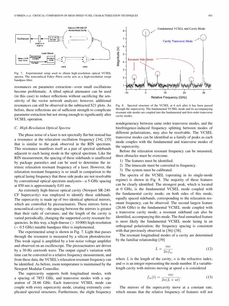
Fig. 7. Experimental setup used to obtain high-resolution optical VCSELspectra. The nonconfocal Fabry–Pérot cavity acts as a high-resolution sweptbandpass filter.
resonances on parameter extraction—even small oscillationsbecome problematic. A tilted optical attenuator can be used(in this case) to reduce reflections without sacrificing the sen-sitivity of the vector network analyzer; however, additionalresonances can still be observed in the subtracted S21 plots. Asbefore, these reflections are of sufficient strength to complicateparameter extraction but not strong enough to significantly alterVCSEL operation.
C. High-Resolution Optical Spectra
The phase noise of a laser is not spectrally flat but instead hasa resonance at the relaxation oscillation frequency [34], [35]that is similar to the peak observed in the RIN spectrum.This resonance manifests itself as a pair of spectral sidebandsadjacent to each lasing mode in the optical spectrum. Like theRIN measurement, the spacing of these sidebands is unaffectedby package parasitics and can be used to determine the in-trinsic relaxation resonant frequency of a laser. However, therelaxation resonant frequency is so small in comparison to theoptical lasing frequency that these side peaks are not resolvableby conventional optical spectrum analyzers—a 5-GHz spacingat 850 nm is approximately 0.01 nm.
An extremely high-finesse optical cavity (Newport SR-240-CF Supercavity) was employed to identify these sidebands.The supercavity is made up of two identical spherical mirrors,which are controlled by piezoactuators. These mirrors form anonconfocal cavity—the spacing between the mirrors is greaterthan their radii of curvature, and the length of the cavity isvaried periodically, changing the supported cavity resonant fre-quencies. In this way, a high-finesse (> 10 000) high-resolution(< 0.5 GHz) tunable bandpass filter is implemented.
The experimental setup is shown in Fig. 7. Light that passesthrough the resonator is measured by a silicon photodetector.This weak signal is amplified by a low-noise voltage amplifierand observed on an oscilloscope. The piezoactuators are drivenby a 30-Hz sawtooth wave. The output signal’s variation withtime can be converted to a relative frequency measurement, andfrom these data, the VCSEL’s relaxation resonant frequency canbe identified. As before, room temperature is maintained by theNewport Modular Controller.
The supercavity supports both longitudinal modes, witha spacing of 7853 GHz, and transverse modes with a sep-aration of 28.66 GHz. Each transverse VCSEL mode cancouple with every supercavity mode, creating extremely com-plicated spectral structures. Furthermore, the slight frequency
Fig. 8. Spectral structure of the VCSEL at 6 mA after it has been passedthrough the supercavity. The fundamental VCSEL mode and its accompanyingresonant side modes are coupled into the fundamental and first-order transversecavity modes.
nondegeneracy between same order transverse modes, and thebirefringence-induced frequency splitting between modes ofdifferent polarizations, may also be resolvable. The VCSELtransverse modes can be identified as a family of peaks as eachmode couples with the fundamental and transverse modes ofthe supercavity.
Before the relaxation resonant frequency can be measured,three obstacles must be overcome.
1) The features must be identified.2) The timescale must be converted to frequency.3) The system must be calibrated.The spectra of the VCSEL (operating in its single-mode
regime) is shown in Fig. 8. The majority of these featurescan be clearly identified. The strongest peak, which is locatedat 0 GHz, is the fundamental VCSEL mode coupled withthe fundamental cavity mode; on both sides of this mode,equally spaced sidebands, corresponding to the relaxation res-onant frequency, can be observed. The second largest feature(28.66 GHz) is the fundamental VCSEL mode coupled witha transverse cavity mode; a resonant sideband can also beidentified, accompanying this mode. The final unmarked featureis most likely the fundamental VCSEL mode lasing in anorthogonal polarization; the frequency spacing is consistentwith that previously observed in [36]–[38].
The resonant longitudinal modes of a cavity are determinedby the familiar relationship [39]
L =mc
2nfm(12)
where L is the length of the cavity; n is the refractive index;andm is an integer representing the mode number. If a variable-length cavity with mirrors moving at speed u is considered
fm(t) =mc
2n(L+ ut). (13)
The mirrors of the supercavity move at a constant rate,which means that the relative frequency of features will not
602 JOURNAL OF LIGHTWAVE TECHNOLOGY, VOL. 25, NO. 2, FEBRUARY 2007
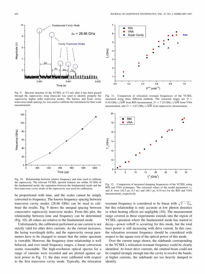
Fig. 9. Spectral structure of the VCSEL at 5.5 mA after it has been passedthrough the supercavity; long timescale was used to identify properly thesupercavity higher order transverse modes. The known, and fixed, cavitytransverse-mode spacing ∆ν was used to calibrate the instrument for finer scalemeasurements.
Fig. 10. Relationship between relative frequency and time used to calibratethe supercavity. The relevant VCSEL spectral features are within 10 GHz ofthe fundamental mode; the separation between the fundamental mode and thefirst transverse cavity mode of the supercavity was used for calibration.
be proportional with time, and the scales cannot be simplyconverted to frequency. The known frequency spacing betweentransverse cavity modes (28.66 GHz) can be used to cali-brate the results. Fig. 9 shows the unequal spacing betweenconsecutive supercavity transverse modes. From this plot, therelationship between time and frequency can be determined(Fig. 10); all values are relative to the fundamental mode.
Unfortunately, the calibration performed at one current is notstrictly valid for other drive currents. As the current increases,the lasing wavelength drifts, and the supercavity sweep para-meters have to be changed to ensure that the entire spectrumis viewable. However, the frequency–time relationship is wellbehaved, and over small frequency ranges, a linear conversionseems reasonable. The high-resolution optical spectra for arange of currents were recorded and are plotted against op-tical power in Fig. 11; the data were calibrated with respectto the first transverse cavity mode. Typically, the relaxation
Fig. 11. Comparison of relaxation resonant frequencies of the VCSELmeasured using three different methods. The extracted slopes are D =
6.93 GHz/√
mW from RIN measurement, D = 7.25 GHz/√
mW from VNAmeasurement, and D = 5.67 GHz/
√mW from supercavity measurement.
Fig. 12. Comparison of measured damping frequencies of the VCSEL usingRIN and VNA techniques. The extracted values of the model parameters τn
and K were 62.5 ps, 0.3 ns and 68.1 ps, 0.34 ns for the RIN and VNAmeasurements, respectively.
resonant frequency is considered to be linear with√I − Ith,
but this relationship is only accurate at low photon densitiesor when heating effects are negligible [16]. The measurementrange covered in these experiments extends into the region ofVCSEL operation where the fundamental mode has started todecay—power rolloff is occurring for this mode, but the totallaser power is still increasing with drive current. In this case,the relaxation resonant frequency should be considered withrespect to the square root of the optical power of this mode.
Over the current range shown, the sidebands correspondingto the VCSEL’s relaxation resonant frequency could be clearlyidentified. At lower drive currents, the emitted beam could notbe coupled strongly enough into the cavity to resolve the bands;at higher currents, the sidebands are too heavily damped toidentify.
O’BRIEN et al.: CRITICAL COMPARISON OF HIGH-SPEED VCSEL CHARACTERIZATION TECHNIQUES 603
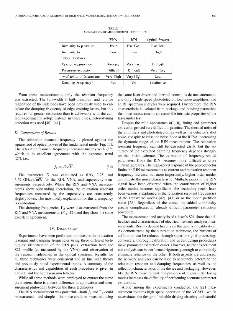
TABLE ICOMPARISON OF MEASUREMENT TECHNIQUES
From these measurements, only the resonant frequencywas extracted. The full-width at half-maximum and relativemagnitude of the sidelobes have been previously used to cal-culate the damping frequency of edge-emitting lasers, but thisrequires far greater resolution than is achievable with the cur-rent experimental setup; instead, in these cases, heterodyningdetection was used [40], [41].
D. Comparison of Results
The relaxation resonant frequency is plotted against thesquare root of optical power of the fundamental mode (Fig. 11).The relaxation resonant frequency increases linearly with
√P ,
which is in excellent agreement with the expected trend[27], i.e.,
fr = D√P . (14)
The parameter D was calculated as 6.93, 7.25, and5.67 GHz/
√mW for the RIN, VNA, and supercavity mea-
surements, respectively. While the RIN and VNA measure-ments show outstanding correlation, the relaxation resonantfrequencies measured by the supercavity are consistentlyslightly lower. The most likely explanation for this discrepancyis calibration.
The damping frequencies Γd were also extracted from theRIN and VNA measurements (Fig. 12), and they show the sameexcellent agreement.
IV. DISCUSSION
Experiments have been performed to measure the relaxationresonant and damping frequencies using three different tech-niques: identification of the RIN peak, extraction from theS21 profile (as measured by the VNA), and observation ofthe resonant sidebands in the optical spectrum. Results forall three techniques were consistent and in line with theoryand previously noted experimental trends. A summary of thecharacteristics and capabilities of each procedure is given inTable I, and further discussion follows.
While all three methods were employed to extract the sameparameters, there is a stark difference in application and mea-surement philosophy between the three techniques.
The RIN measurement was powerful—both fr and Γd couldbe extracted—and simple—the noise could be measured using
the same laser driver and thermal control as dc measurements,and only a high-speed photodetector, low-noise amplifiers, andan RF spectrum analyzer were required. Furthermore, the RINcharacteristic is isolated from package and bonding parasitics;the noise measurement represents the intrinsic properties of thelaser under test.
Despite the mild appearance of (10), fitting and parameterextraction proved very difficult in practice. The thermal noise ofthe amplifiers and photodetector, as well as the detector’s shotnoise, conspire to raise the noise floor of the RFSA, decreasingthe dynamic range of the RIN measurement. The relaxationresonant frequency can still be extracted easily, but the ac-curacy of the extracted damping frequency depends stronglyon the initial estimate. The extraction of frequency-relatedparameters from the RIN becomes more difficult as drivecurrent increases. The high-speed response of the photodetectorlimits the RIN measurements as current and relaxation resonantfrequency increase, but more importantly, higher order modescomplicate the noise characteristic. Multiple peaks in the RINsignal have been observed when the contribution of higherorder modes becomes significant; the secondary peaks havebeen variously explained as the relaxation resonant frequenciesof the transverse modes [42], [43] or as the mode partitionnoise [28]. Regardless of the cause, the added complexitygreatly complicates an already difficult parameter extractionprocedure.
The measurement and analysis of a laser’s S21 share the dif-ficulties and characteristics of electrical network analyzer mea-surements: Results depend heavily on the quality of calibration.As demonstrated by the subtraction technique, the burdens ofcalibration can be reduced through superior signal processing;conversely, thorough calibration and circuit design proceduresmake parameter extraction easier. However, neither experimentnor analysis can be performed rigorously enough to completelyeliminate reliance on the other. If both aspects are addressed,the network analyzer can be used to accurately determine therelaxation resonant and damping frequencies, as well as thereflection characteristics of the device and packaging. However,like the RIN measurement, the presence of higher order lasingmodes increases the difficulty of performing accurate parameterextractions.
Alone among the experiments conducted, the S21 mea-surement requires high-speed operation of the VCSEL, whichnecessitates the design of suitable driving circuitry and careful

604 JOURNAL OF LIGHTWAVE TECHNOLOGY, VOL. 25, NO. 2, FEBRUARY 2007
consideration of calibration points. Once the initial designissues have been overcome, the S21 is an extremely simplemeasurement to make. This technique benefits greatly from thelegacy of microwave measurements and accumulated knowl-edge, and unlike high-finesse optical cavities, network analyz-ers are ubiquitous in laboratory environments.
Despite the power and availability of network analyzers,the S21 is an inherently nonideal measurement for this par-ticular application (extraction of intrinsic laser parameters).The VCSEL’s transfer function is complicated by package andbonding parasitics, which are nontrivial to remove. The useof a probing station on VCSEL chips reduces the problemscaused by parasitics but does not eliminate them completely.If possible, it is far more appealing to measure the intrinsicparameters directly. The network analyzer measurements seemmore suitable for use in higher level analysis, such as integratedtransmitter characterization, in which the parasitic response isas important as the VCSEL characteristics.
Analysis of the optical spectrum is neither as popular noras powerful as the previous two measurement techniques. Thesidebands are spaced too closely to resolve with conventionalinstruments, and only the relaxation resonant frequency can beeasily determined from these bands. The relative strength of thepeaks decreases with drive current, indicating that the dampingfrequency could also be calculated if sufficient resolution couldbe achieved.
In measuring the relaxation resonant frequency alone, spec-tral analysis is a very attractive procedure. The phase noise isisolated from package parasitics; the bulk of the experimentalsetup is shared with the dc characterization procedures; opticalpower is measured at dc, and thus, the operational range is notlimited by the speed of the photodetector; and time-consumingparameter extractions are avoided, as the relaxation resonantfrequency can be determined almost immediately from theinitial data. Unfortunately, the supercavity employed is neitheruser friendly, flexible, nor robust; calibration is a problem area,and the optical sidebands are weak and difficult to identify. Theimplementation of a heterodyning spectrum analyzer, insteadof a supercavtiy, could reduce these problems but will noteliminate them; in addition, the damping frequency could alsobe extracted.
For all its difficulties, this technique seems verypromising—it addresses the shortcomings of other measure-ments. In amplitude-based measurements, such as the RIN andS21, the contributions of transverse modes are superimposedand unresolvable; in spectral measurements, the modes remainspectrally separated and can easily be distinguished from eachother. The lasing of higher order modes will not hinder themeasurement of the fundamental mode’s relaxation resonantfrequency. In fact, if sufficient power could be coupled fromthe transverse modes, the relaxation resonant frequency of eachmode could be measured simultaneously.
V. CONCLUSION
The S21 measurement is, in essence, electrical, and it inheritsthe familiar difficulties and requirements, namely well-matcheddriving circuitry, low attenuation at all frequencies, and rigor-
ous calibration conducted as close to the device as possible.By contrast, the supercavity provides an optical measurement;success relies heavily on alignment, mode matching, couplingpower, and quality of optical components. The RIN measure-ment falls somewhere in between—it measures a fundamentaloptical characteristic (spontaneous emission) but in the elec-trical domain. Through this fortunate combination, it is onlyslightly burdened by either electrical or optical concerns.
In the final analysis, the supercavity measurement seems tobe the most promising and underdeveloped; the VNA measure-ment is the most convenient and familiar; and the RIN measure-ment is the most robust. The three techniques provide consistentresults but possess clear advantages for various situations.
REFERENCES
[1] M. Forbes, J. Gourlay, and M. Desmulliez, “Optically interconnectedelectronic chips: A tutorial and review of the technology,” Electron.Commun. Eng. J., vol. 13, no. 5, pp. 221–231, Oct. 2001.
[2] S. Tang, R. T. Chen, L. Garrett, D. Gerold, and M. M. Li, “Designlimitations of highly parallel free-space optical interconnects based onarrays of vertical cavity surface-emitting laser diodes, microlenses andphotodetectors,” J. Lightw. Technol., vol. 12, no. 11, pp. 1971–1975,Nov. 1994.
[3] N. McArdle, M. Naruse, and M. Ishikawa, “Optoelectronic parallelcomputing using optically interconnected pipelined processing arrays,”IEEE J. Sel. Topics Quantum Electron., vol. 5, no. 2, pp. 250–260,Mar./Apr. 1999.
[4] Y. Liu, “Heterogeneous integration of OE arrays with Si electronicsand microoptics,” IEEE Trans. Adv. Packag., vol. 25, no. 1, pp. 43–49,Feb. 2002.
[5] L. A. Coldren, O. Sjolund, D. A. Louderback, S. Nakagawa, andE. R. Hegblom, “Flip-chip bonded, back emitting, microlensed arrays ofmonolithic vertical cavity lasers and resonant photodetectors,” in Proc.Electron. Compon. Technol. Conf., 1999, pp. 733–740.
[6] A. Karim, J. Piprek, P. Abraham, D. Lofgreen, Y. Chiu, and J. E.Bowers, “1.55-um vertical-cavity laser arrays for wavelength-divisionmultiplexing,” IEEE J. Quantum Electron., vol. 7, no. 2, pp. 178–183,Mar./Apr. 2001.
[7] L. A. Coldren, Diode Lasers and Photonic Integrated Circuits. NewYork: Wiley, 1995.
[8] J. E. Bowers, “High speed semiconductor laser design and performance,”Solid-State Electron., vol. 30, no. 1, pp. 1–11, Jan. 1987.
[9] K. Petermann, Laser Diode Modulation and Noise. Norwell, MA:Kluwer, 1991.
[10] S. Z. Zang, N. M. Margalit, T. E. Reynolds, and J. E. Bowers, “1.54 µmvertical-cavity surface-emitting laser transmission at 2.5 GB/s,” IEEEPhoton. Technol. Lett., vol. 9, no. 3, pp. 374–376, Mar. 1997.
[11] K. Czotscher, S. Weisser, A. Levin, and J. Rosenzweig, “Intensitymodulation and chirp of 1.55-um multiple-quantum-well laser diodes:Modeling and experimental verification,” IEEE J. Sel. Topics QuantumElectron., vol. 5, no. 3, pp. 606–612, May/Jun. 1999.
[12] K. A. Black, E. S. Bjorlin, J. Piprek, E. Hu, and J. E. Bowers, “Small-signal frequency response of long-wavelength vertical-cavity lasers,”IEEE Photon. Technol. Lett., vol. 13, no. 10, pp. 1049–1051, Oct. 2001.
[13] M. Bruensteiner and G. C. Papen, “Extraction of VCSEL rate-equationparameters for low bias system simulation,” IEEE J. Sel. Topics QuantumElectron., vol. 5, no. 3, pp. 487–494, May/Jun. 1999.
[14] J. K. Guenter, J. A. Tatum, A. Clark, R. S. Penner, R. H. Johnson,R. A. Hawthorne, J. R. Biard, and Y. Liu, “Commercialization ofHoneywell’s VCSEL technology: Further developments,” Proc. SPIE,vol. 4286, no. 1, pp. 1–14, 2001.
[15] L. Bjerkan, A. Royset, L. Hafskjaer, and D. Myhre, “Measurement of laserparameters for simulation of high-speed fiberoptic systems,” J. Lightw.Technol., vol. 14, no. 5, pp. 839–850, May 1996.
[16] G. Guekos, Photonic Devices for Telecommunications: How to Model andMeasure. Berlin, Germany: Springer-Verlag, 1999.
[17] D. Tauber, G. Wang, R. S. Geels, J. E. Bowers, and L. A. Coldren, “Largeand small signal dynamics of vertical cavity surface emitting lasers,” Appl.Phys. Lett., vol. 62, no. 4, pp. 325–327, Jan. 1993.
[18] S. Jiang, M. Dagenais, and R. A. Morgan, “Optical spectrum sidebandsof a vertical-cavity surface-emitting laser,” in Proc. IEEE/LEOS Annu.Meeting, 1994, vol. 1, pp. 278–279.

O’BRIEN et al.: CRITICAL COMPARISON OF HIGH-SPEED VCSEL CHARACTERIZATION TECHNIQUES 605
[19] K. Vahala, C. Harder, and A. Yariv, “Observation of relaxation resonanceeffects in the field spectrum of semiconductor lasers,” Appl. Phys. Lett.,vol. 42, no. 3, pp. 211–213, Feb. 1983.
[20] C. H. Henry, “Theory of the phase noise and power spectrum of a singlemode injection laser,” IEEE J. Quantum Electron., vol. QE-19, no. 9,pp. 1391–1397, Sep. 1983.
[21] ——, “Phase noise in semiconductor lasers,” J. Lightw. Technol.,vol. LT-4, no. 3, pp. 298–311, Mar. 1986.
[22] T. E. Darcie, R. S. Tucker, and G. J. Sullivan, “Intermodulation andharmonic distortion in InGaAsP lasers,” Electron. Lett., vol. 21, no. 16,pp. 665–666, Aug. 1985.
[23] M. Majewski and L. Coldren, “Distortion characteristics in directly mod-ulated laser diodes by microwave signals,” in IEEE MTT-S Int. Microw.Symp. Dig., 1989, pp. 1167–1170.
[24] K. Petermann, “External optical feedback phenomena in semi-conductor lasers,” IEEE J. Sel. Topics Quantum Electron., vol. 1, no. 2,pp. 480–489, Jun. 1995.
[25] G. E. Obarski and P. D. Hale, “How to measure relative intensity noise inlasers,” Laser Focus World, vol. 35, no. 5, pp. 273–277, May 1999.
[26] D. M. Kuchta, J. Gamelin, J. D. Walker, J. Lin, K. Y. Lau, J. S. Smith,M. Hong, and J. P. Mannaerts, “Relative intensity noise of vertical cavitysurface emitting lasers,” Appl. Phys. Lett., vol. 62, no. 11, pp. 1194–1196,Mar. 1993.
[27] M. C. Tatham, I. F. Lealman, C. P. Seltzer, L. D. Westbrook, andD. M. Cooper, “Resonance frequency, damping, and differential gainin 1.5 µm multiple quantum-well lasers,” IEEE J. Quantum Electron.,vol. 28, no. 2, pp. 408–414, Feb. 1992.
[28] L.-G. Zei, S. Ebers, J.-R. Kropp, and K. Petermann, “Noise performanceof multimode VCSELs,” J. Lightw. Technol., vol. 19, no. 6, pp. 884–892,Jun. 2001.
[29] P. S. Spencer, C. R. Mirasso, and K. A. Shore, “Effect of strong op-tical feedback on vertical-cavity surface-emitting lasers,” IEEE Photon.Technol. Lett., vol. 10, no. 2, pp. 191–193, Feb. 1998.
[30] T. Kondo, M. Arai, A. Matsutani, T. Miyamoto, and F. Koyama, “Iso-lator free 10 Gb/s singlemode fibre data transmission using 1.1 µmGaInAs/GaAs vertical cavity surface emitting laser,” Electron. Lett.,vol. 40, no. 1, pp. 65–66, Jan. 2004.
[31] P. B. Subrahmanyam, Y. Zhou, L. Chrostowski, and C. J. Chang-Hasnain,“VCSEL tolerance to optical feedback,” Electron. Lett., vol. 41, no. 21,pp. 1178–1179, Oct. 2005.
[32] J. W. Bae, H. Temkin, S. E. Swirhun, W. E. Quinn, P. Brusenbach,C. Parsons, M. Kim, and T. Uchida, “Reflection noise in vertical cavitysurface emitting lasers,” Appl. Phys. Lett., vol. 63, no. 11, pp. 1480–1482,Sep. 1993.
[33] P. A. Morton, T. Tanbun-Ek, R. A. Logan, A. M. Sergent, P. F. Sciortino,and D. L. Coblentz, “Frequency response subtraction for simple measure-ment of intrinsic laser dynamic properties,” IEEE Photon. Technol. Lett.,vol. 4, no. 2, pp. 133–136, Feb. 1992.
[34] S. Piazzolla, P. Spano, and M. Tamburrini, “Characterization ofphase noise in semiconductor lasers,” Appl. Phys. Lett., vol. 41, no. 8,pp. 695–696, Oct. 1982.
[35] B. Daino, P. Spano, M. Tamburrini, and S. Piazzolla, “Phase noise andspectral line shape in semiconductor lasers,” IEEE J. Quantum Electron.,vol. QE-19, no. 3, pp. 266–270, Mar. 1983.
[36] A. K. J. V. Doorn, M. P. V. Exter, and J. P. Woerdman, “Effects oftransverse anisotropy on VCSEL spectra,” Electron. Lett., vol. 30, no. 23,pp. 1941–1943, Nov. 1994.
[37] J. E. Epler, S. Gehrsitz, K. H. Gulden, M. Moser, H. C. Sigg, andH. W. Lehmann, “Mode behavior and high resolution spectra of circularly-symmetric GaAs–AlGaAs air-post vertical cavity surface emitting lasers,”Appl. Phys. Lett., vol. 69, no. 6, pp. 722–724, Aug. 1996.
[38] F. Robert, P. Besnard, M. L. Charès, and G. M. Stéphan, “Switching of thepolarization state of a vertical cavity surface-emitting laser using polarizedfeedback,” Opt. Quantum Electron., vol. 27, no. 9, pp. 805–811, 1995.
[39] J. T. Verdeyen, Laser Electronics. Englewood Cliffs, NJ: Prentice-Hall,1995.
[40] R. J. Lang, H. P. Meyer, H. Schweizer, and A. P. Mozer, “Measurementof relaxation resonance, damping, and nonlinear gain coefficient from thesidebands in the field spectrum of a 1.3 µm InGaAsP distributed feedbacklaser,” Appl. Phys. Lett., vol. 54, no. 19, pp. 1845–1847, May 1989.
[41] M. P. V. Exter, W. A. Hamel, J. P. Woerdman, and B. R. P. Zeijlmans,“Spectral signature of relaxation oscillations in semiconductor lasers,”IEEE J. Quantum Electron., vol. 28, no. 6, pp. 1470–1478, Jun. 1992.
[42] Y. Satuby and M. Orenstein, “Small-signal modulation of multitrans-verse modes vertical-cavity surface-emitting semiconductor lasers,” IEEEPhoton. Technol. Lett., vol. 10, no. 6, pp. 757–759, Jun. 1998.
[43] A. Valle and L. Pesquera, “Relative intensity noise of multitransversemode vertical cavity surface emitting lasers,” in Proc. CLEO, 1999,pp. 175–176.
Christopher J. O’Brien was born in Adelaide, S.A., Australia, in 1980. Hereceived the B.Eng. (Elec.) and Ph.D. degrees in electrical engineering fromthe University of Queensland, Brisbane, Qld., Australia, in 2001 and 2006,respectively.
His primary research interests are the experimental investigation and model-ing of vertical-cavity surface-emitting lasers, particularly in a free-space opticalinterconnect environment.
Marian L. Majewski, photograph and biography not available at the time ofpublication.
Aleksandar D. Rakic (S’94–M’95) received the Dipl.-Ing. degree in electricalengineering/engineering physics and the M.Eng.Sci. degree in optoelectronicsfrom the University of Belgrade, Belgrade, Yugoslavia, and the Ph.D. degreein electrical engineering from the University of Queensland, Brisbane, Qld.,Australia.
He is the Director of electrical engineering and a Senior Lecturer with theSchool of Information Technology and Electrical Engineering, University ofQueensland. He has coauthored more than 120 research articles and one bookchapter.
Dr. Rakic served as the General Chair for the 2004 Conference on Opto-electronic and Microelectronic Materials and Devices (COMMAD04) and theCo-Chair of the Symposium on Molecular and Organic Electronics and Or-ganic Displays within the 2006 International Conference on Nanoscience andNanotechnology (ICONN 2006). He has been involved as a Program Commit-tee Member with a number of photonics and optical materials conferences.