Embed Size (px)
Citation preview

A Digital VLSI Architecture forReal-World Applications
Dan Hammerstrom
INTRODUCTION
As the other chapters of this book show, the neuralnetwork model has significant advantages over tradi-tional mcdels for certain applications. It has also ex-panded our understanding of biological neural net-works b> providing a theoretical foundation and a setof functional models.
.Neural network simulation remains a computa-tional]!. intensive activity, however. The underlyingcomputations-generally multiply-accumulates-aresimple but numerous. For example, in a simple artifi-cial neural network (ANN) model, most nodes areconnected to most other nodes, leading to O(W) COKZ-necrions: A network with 100,000 nodes, modest bybiological standards, would therefore have about 10billion connections, with a multiply-accumulate oper-ation needed for each connection. If a state-of-the-artworkstation can simulate roughly 10 million connec-
‘The “o&r of” O(F(n)) notation means that the quantity repre-sented by 0 is approximate for the function F within a multiplica-tion or diGon by n.
tions per second, then one pass through the networktakes 1000 set (about 20 min). This data rate is muchtoo slow for real-time process control or speech rec-ognition, which must update several times a second.Clearly, we have a problem.
This performance bottleneck is worse if each con-nection requires more complex computations, for in-stance, for incremental learning algorithms or for morerealistic biological simulations. Eliminating this com-putational barrier has led to much research into build-ing custom Very Large Scale Integration (VLSI)silicon chips optimized for ANNs. Such chips mightperform ANN simulations hundreds to thousands oftimes faster than workstations or personal comput-ers-for about the same cost.
The research into VLSI chips for neural networkand pattern recognition applications is based on thepremise that optimizing the chip architecture to thecomputational characteristics of the problem letsthe designer create a silicon device offering a big im-provement in performance/cost or “operations per dol-lar.” In silicon design, the cost of a chip is primarilydetermined by its two-dimensional area. Smaller chips
L ,_.‘Llr iuwductm to Neural and Electronic Networks, Second Edition. Copyright Q 1995 by Academic Press, Inc. All rights of reproduction in any forin resewed.
335

336 Dan Hammerstrom ;,
are cheaper chips. Within a chip, the cost of an opera-tion is roughly determined by the silicon area neededto implement it. Furthermore, speed and cost usuallyhave an inverse relationship: faster chips are generallybigger chips.
The silicon designer’s goal is to increase the numberof operations per unit area of silicon, calledfunctionaldensity, in turn, increasing operations per dollar. Anadvantage of ANN, pattern recognition, and imageprocessing algorithms is that they employ simple, low-precision operations requiring little silicon area. As aresult, chips designed for ANN emulation can have ahigher functional density than traditional chips such asmicroprocessors. The motive for developing special-ized chips, whether analog or digital, is this potentialto improve performance, reduce cost, or both.
The designer of specialized silicon faces many otherchoices and trade-offs. One of the most important isflexibility versus speed. At the “specialized” end ofthe flexibility spectrum, the designer gives up versatil-ity for speed to make a fast chip dedicated to one task.At the “general purpose” end, the sacrifice is reversed,yielding a slower, but programmable device. Thechoice is difficult because both traits are desirable.Real-world neural network applications ultimatelyneed chips across the entire spectrum.
This chapter reviews one such architecture, CNAPS2(Connected Network of Adaptive Processors), devel-oped by Adaptive Solutions, Inc. This architecture wasdesigned for ANN simulation, image processing, andpattern recognition. To be useful in these related con-texts, it occupies a point near the “general purpose”end of the flexibility spectrum. We believe that, for itsintended markets, the CNAPS architecture has theright combination of speed and flexibility. One reasonfor writing this chapter is to provide a retrospectiveon the CNAPS architecture after several years’ ex-perience developing software and applications for it.
The chapter has three major sections, each framedin terms of the capabilities needed in the CNAPS com-puter’s target markets. The first section presents an
‘Trademark Adaptive Solutions, Inc.
overview of the CNAPS architecture and offers a ra-tionale for its major design decisions. It also sum-marizes the architecture’s limitations and describesaspects that, in hindsight. its designers might havedone differently. The section ends with a brief dis-cussion of the software developed for the machineso far.
The second section briefly reviews applications de-veloped for CNAPS at this writing.’ The applicationsdiscussed are simple image processing, automatic tar-get recognition, a simulation of the Lynch/GrangerPyriform Model, and Kanji OCR. Finally. to offer abroader perspective of real-world ANN usage. thethird section reviews non-CNAPS applications. specif-ically, examples of process control and financialanalysis.
THE CNAPSARCHITECTURE
The CNAPS architecture consists of an array’ of pro-cessors controlled by a sequencer. both implementedas a chip set developed by Adaptive Solutions. Inc.The sequencer is a one-chip device called the CNAPSSequencer Chip (CSC). The processor an-a!- is also aone-chip device, available with either 64 or 16 proces-sors per chip (the CNAPS- 1064 or CNAPS- 10 16). TheCSC can control up to eight 1064s or 1016s. which actlike one large device.
These chips usually sit on a printed circuit boardthat plugs into a host computer, also called the controlprocessor (CP). The CNAPS board acts as a coproces-sor within the host. Under the coprocessor model, thehost sends data and programs to the board. which runsuntil done, then interrupts the host to indicate comple-tion. This style of operation is called “run to comple-tion semantics.” Another possible model is to use theCNAPS board as a stand-alone device to process datacontinuously.
3Because ANNs are becoming a key technology. many customersconsider their use of ANNs to be proprietary information. Manyapplications are not yet public knowledge.

17. Digital VLSI Architecture for Real-World Problems
The CNAPS Architecture
Basic Structure
CNAPS is a single instruction, multiple data stream(SIMD) architecture. A SIMD computer has one in-struction sequencing/control unit and many processornodes (PNs). In CNAPS, the PNs are connected in aone-dimensional array (Figure 1) in which each PNcan “talk” only to its right or left neighbors. The se-quencer broadcasts each instruction plus input data toall PNs. which execute the same instruction at eachclock. The PNs transmit output data to the sequencer,with se\.eral arbitration modes controlling access tothe output bus.
As Figure 2 suggests, each PN has a local memory,4a multiplier, an adder/subtracter, a shifter/logic unit, aregister tile,’ and a memory addressing unit. The entirePN uses fixed-point, two’s complement arithmetic, andthe precision is 16 bits, with some exceptions. The PNmemory can handle 8- or 16-bit reads or writes. Themultiplier produces a 24-bit output; an 8 X 16 or 8 X8 multiply takes one clock, and a 16 X 16 multiplytakes two clocks. The adder can switch between 16- or32-bit modes. The input and output buses are 8 bitswide, and a 16-bit word can be assembled (or disas-sembled! from two bytes in two clocks.
A P5 has several additional features (Hammer-Strom. 1990, 1991) including a function that finds thePN with the largest or smallest values (useful forwinner-take-all and best-match operations), variousprecision and memory control features, and OutBusarbitration. These features are too detailed to discussfully here.
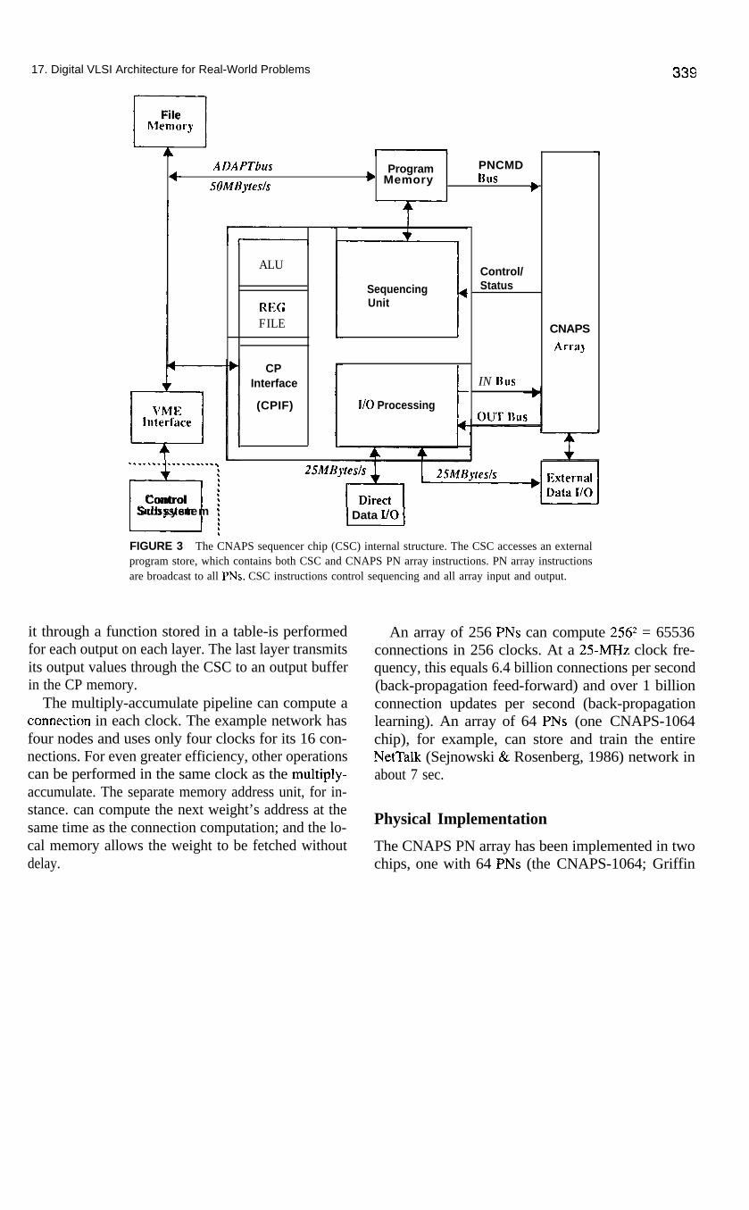
The CSC sequencer (Figure 3) performs programsequencing for the PN array and has private accessto a program memory. The CSC also performs input/output (l/O) processing for the array, writing inputdata to the array and reading output data from it. Tomove data to and from CP memory, the CSC has a 32-bit bus, called the AdaptBus, on the CP side. The CSC
d Currently 4 KB per PN.5 Currently 32, 16-bit registers.
also has a direct input port and aused to connect the CSC directlyhigher-bandwidth data movement.
Neural Network Example
337
direct output portto I/O devices for
The CNAPS architecture can run many ANN and non-ANN algorithms. Many SIMD techniques are the samein both contexts, so an ANN can serve as a generalexample of mapping an algorithm to the &-ray. Specif-ically, the example here shows how the PN array sim-ulates a layer in an ANN.
Start by assuming a two-layered network (Figure 4)in which-for simplicity-each node in each layermaps to one PN. PN, thus simulates the node n,;, wherei is the node index in the layer andj is the layer index.Layers are simulated in a time-multiplexed manner.All layer 1 nodes thus execute as a block, then all layer2 nodes, and so on. Finally, assume that layer 1 hasalready calculated its various n,,, outputs.
The goal at this point is to calculate the outputs forlayer 2. To achieve this, all layer 1 PNs simultaneouslyload their output values into a special output bufferand begin arbitration for the output bus. In this case,the arbitration mode lets each PN transmit its output insequence. In one clock, the content of PN,‘s buffer isplaced on the output bus and goes through the se-quencer6 to the input bus. From the input bus, thevalue is broadcast to all PNs (this out-to-in loopbackfeature is a key to implementing layered structures ef-ficiently). Each PN then multiplies node n,,‘s outputwith a locally stored weight, w,,~.
On the next clock, node n,,,‘s output is broadcast toall PNs, and so on for the remaining layer 1 outputvalues. After N clocks, all outputs have been broad-cast, and the inner product computation is complete.All PNs then use the accumulated value’s most signif-icant 8 bits to look up an &bit nonlinear output valuein a 256-item table stored in each PN’s local memory.This process-calculating a weighted sum, then passing
hThis operation actually takes several clocks and must be pipe-lined. These details are eliminated here for clarity.

338 Dan Hammerstrom
OUTBus
PNCMDBus
D
INI
Bus
CNAPS
I
Inter-PN4 PNO- PNl .a............... PNfjj-Bus
AA A4 AA
131r
CNAPS
FIGURE 1 The basic CNAPS architecture. CNAPS is a single instruction, multiple data (SIMD)architecture that uses broadcast input, one-dimensional interprocessor communication, and a singleshared output bus.
A Bus 16
B Bus, 16
2 I
w *outputUnit
&A
,InputUnit
Inter-PN Bus , 4 (2 in, 2 out)I b
2
PNCMD Bus
IN Bus
131 b
+FIGURE 2 The internal structure of a CNAPS processor node (PN). Each PN has its own storageand arithmetic capabilities. Storage consists of 4096 bytes. Arithmetic operations include multiply,accumulate, logic, and shift. All units are interconnected by two 16-bit buses.
17. Digital VLSI Architecture for Real-World Problems 339
l--lFileMenior~
Al.AYTlws4-
Program PNCMD
SOMll~Vesls + Memory BUSb
. ..-... . .._..._\.\
tl ::Control i
Subsystem ::,
ALU
REGFILE
CPInterface
(CPIF)
SequencingUnit
I/O Processingt
Control/Status
IN Bus
CNAPSArra)
1 Data L/O]
FIGURE 3 The CNAPS sequencer chip (CSC) internal structure. The CSC accesses an externalprogram store, which contains both CSC and CNAPS PN array instructions. PN array instructionsare broadcast to all PNs. CSC instructions control sequencing and all array input and output.
it through a function stored in a table-is performedfor each output on each layer. The last layer transmitsits output values through the CSC to an output bufferin the CP memory.
The multiply-accumulate pipeline can compute aconnection in each clock. The example network hasfour nodes and uses only four clocks for its 16 con-nections. For even greater efficiency, other operationscan be performed in the same clock as the multiply-accumulate. The separate memory address unit, for in-stance. can compute the next weight’s address at thesame time as the connection computation; and the lo-cal memory allows the weight to be fetched withoutdelay.
An array of 256 PNs can compute 256* = 65536connections in 256 clocks. At a 25-MHz clock fre-quency, this equals 6.4 billion connections per second(back-propagation feed-forward) and over 1 billionconnection updates per second (back-propagationlearning). An array of 64 PNs (one CNAPS-1064chip), for example, can store and train the entireNetTalk (Sejnowski & Rosenberg, 1986) network inabout 7 sec.
Physical Implementation
The CNAPS PN array has been implemented in twochips, one with 64 PNs (the CNAPS-1064; Griffin

340
CN4 CN5 CN6 CN7
CNO CNl CN2 CN3
Broadcast by PNO of CNO’s output to CN4, 5, 6,7takes 1 clock
N* connections in N clocks
FIGURE 4
f f _ t
CNO CNl CN2 CN3
PNO PNl PN2 PN3
CN4 CN5 CN6 CN7
t t t t
A simple two-layered neural network. In this example,each PN emulates two network nodes. PNs emulate the first layer,computing one connection each clock. Then, they sequentially placenode output on the OutBus while emulating, in parallel, the secondlayer.
et al., 1990 Figure 5) and the other with 16 PNs (theCNAPS-1016). Both chips are implemented in a 0.8micron CMOS process. The 64-PN chip is a full cus-tom design and is approximately 26 mm on a side andhas more than 14 million transistors, making it one ofthe largest processor chips ever made. The simplecomputational model makes possible a small, simplePN, in turn permitting the use of redundancy to im-prove semiconductor yield for such a device.
The CSC is implemented using a gate array technol-ogy, using a lOO,OOO-gate die and is about 10 mm ona side.
The next section reviews the various design deci-sions and the reasons for making them. Some of thefeatures described are unique to CNAPS; others applyto any digital signal processor chip.
Dan Hammerstrom
Major Design DecisionsWhen designing the CNAPS architecture, a key ques-tion was where it should sit relative to other computingdevices in cost and capabilities. In computer design,flexibility and performance are almost always in-versely related. We wanted CNAPS to be flexibleenough to execute a broad family of ANN algorithmsas well as other related pattern recognition and pre-processing algorithms. Yet, we wanted it to have muchhigher performance than state-of-the-art workstationsand-at the same time-lower cost for its functions.
Figure 6 shows where we are targeting CK_iPS. Thevertical dimension plots each architecture by- its flexi-bility. Flexibility is difficult to quantify, because it in-volves not only the range of algorithms that anarchitecture can execute. but also the complexity ofthe problems it can solve. (Greater complexity typi-cally requires a larger range of operations. I As a re-sult, this graph is subjective and provided only as anillustration.
The horizontal dimension plots each architecture byits performance/cost-or operations per second perdollar. The values are expressed in a log scale due tothe orders-of-magnitude difference between tradi-tional microprocessors at the low end and highly cus-tom, analog chips at the high end. Note the technologybarrier, defined by practical limits of current semicon-ductor manufacturing. No one can build past the bar-rier: you can do only so much with a transistor; youcan put only so many of them on a chip; and you canrun them only so fast.
For pattern recognition, we placed the CN.\PS ar-chitecture in the middle, between the specialized ana-log chips and the general-purpose microprocessors. Wewanted it to be programmable enough to so1L.e manyreal-world problems, and yet have a performance/costabout 100 times faster than the highest performanceRISC processors. The CNAPS applications discussedlater show that we have provided sufficient flexibilityto solve complex problems.
In determining the degree of function required, wemust solve all or most of a targeted problem. This needresults from Amdahl’s law, which states that system

17. Digital VLSI Architecture for Real-World Problems 341
FIGURE 5 The CNAPS PN array chip. There are 64 PNs with memory on each die.The PN array chip is one of the largest processor chips ever made. It consists of 14million transistors and is over 26 mm on a side. PN redundancy, there are 16 sparePNs, is used to guarantee high yields.
performance depends mainly on the slowestnent. This law can be formalized as follows:
s = 1@pi * q> + @p,, * s/J
compo-
(1)
where S is the total system speed-up, op,is the fractionof total operations in the part of the computation runon the f&r chip, sr is the speedup the chip provides,op,, is the fraction of total operations run on the hostcomputer without acceleration. Hence, as opf or sr getlarge, S approaches l/op,,. Unfortunately, opf needs tobe close to one before any real system-level improve-ment occurs, as shown in the following example.
Suppose there are two such support chips to choosefrom: the first can run 80% of the computation with20X improvement on that 80%; the second can runonly 205. but runs that 20% 1000X faster. By Am-dahl’s law. the first chip speeds up the system by morethan 4005, whereas the second-and seemingly fas-ter-chip speeds up the system by only 20%. So Am-dahl tells us that flexibility is often better than rawperformance, especially if that performance results
~ Technology Barrier
and DSPs
CNAPS
\Full CustomDigital/Analog
c
Operations/Dollar
FIGURE 6 Though subjective, this graph gives a rough indicationof the CNAPS market positioning. The vertical dimension measuresthe range of functionality of an architecture; the horizontal dimen-sion measures the performance/cost in operations per second perdollar. The philosophy behind CNAPS is that by restricting func-tionality to pattern recognition, image processing, and neural net-work emulation, a larger performance/cost is possible than withtraditional machines (parallel or sequential).
342from limiting the range of operations performed by thedevice.
Dan Harmerstrom
DigitalMuch effort has been dedicated to building analogVLSI chips for ANNs. Analog chips have great ap-peal, partly because they follow biological modelsmore closely than digital chips. Analog chips also canachieve higher functional density. Excellent papers re-porting research in this area include Mead (1989), Ak-ers, Haghighi, and Rao (1990), Graf, Jackel, andHubbard (1988), Holler, Tam, Castro, and Benson(1989), and Alspector (1991). Also, see Morgan(1990) for a good summary of digital neural networkemulation.
Analog ANN implementations have been primarilyacademic or industrial research projects, however.Only a few have found their way into the real world ascommercial products: getting an analog device to workin a laboratory is one thing; making it work over awide range of voltages, temperatures, and user capa-bilities is another. In general, analog chips requiremuch more stringent operating conditions than digitalchips. They are also more difficult to design and, afterimplementation, less flexible.
The semiconductor industry is heaviIy oriented to-ward digital chips. Analog chips represent only a mi-nor part of the total output, reinforcing their secondaryposition. There are, of course, successful analog parts,and there always will be, because some applicationsrequire analog’s higher functional density to achievetheir cost and performance constraints, and those ap-plications can tolerate analog’s limited flexibility.Likewise, there will be successful products using ana-log ANN chips. Analog parts will probably be used insimple applications, or as a part of a larger system inmore complex applications.
This prediction follows primarily from the limitedflexibility of analog chips. They typically implementone algorithm, hardwired into the chip. A hardwiredalgorithm is fine if it is truly stable and it is all youneed. The field of ANN applications is still new, how-ever, So most complex implementations are still ac-
tively evolving-even at the algorithm level. Ananalog device cannot easily follow such changes. Adigital, programmable device can change algorithmsby changing software.
Our major goal was to produce a commercial prod-uct that would be flexible enough and provide suffi-cient precision to cover a broad range of <omplexproblems. This goal dictated a digital design. becausedigital could offer accurate precision and niush moreflexibility than a typical CMOS analog impismenta-tion. Digital also offered excellent performmce andthe advantages of a standardized technolog!-.
Limited, Fixed-Point Precision
In both analog and digital domains, an impcrrant de-cision is choosing the arithmetic precision rscxired. Inanalog, precision affects design complexit\ Jnd theamount of compensation circuitry required. In digital,it effects the number of wires available as \&?!I as thesize and complexity of memory, buses, and LYthmeticunits. Precision also affects the power dissiparion.
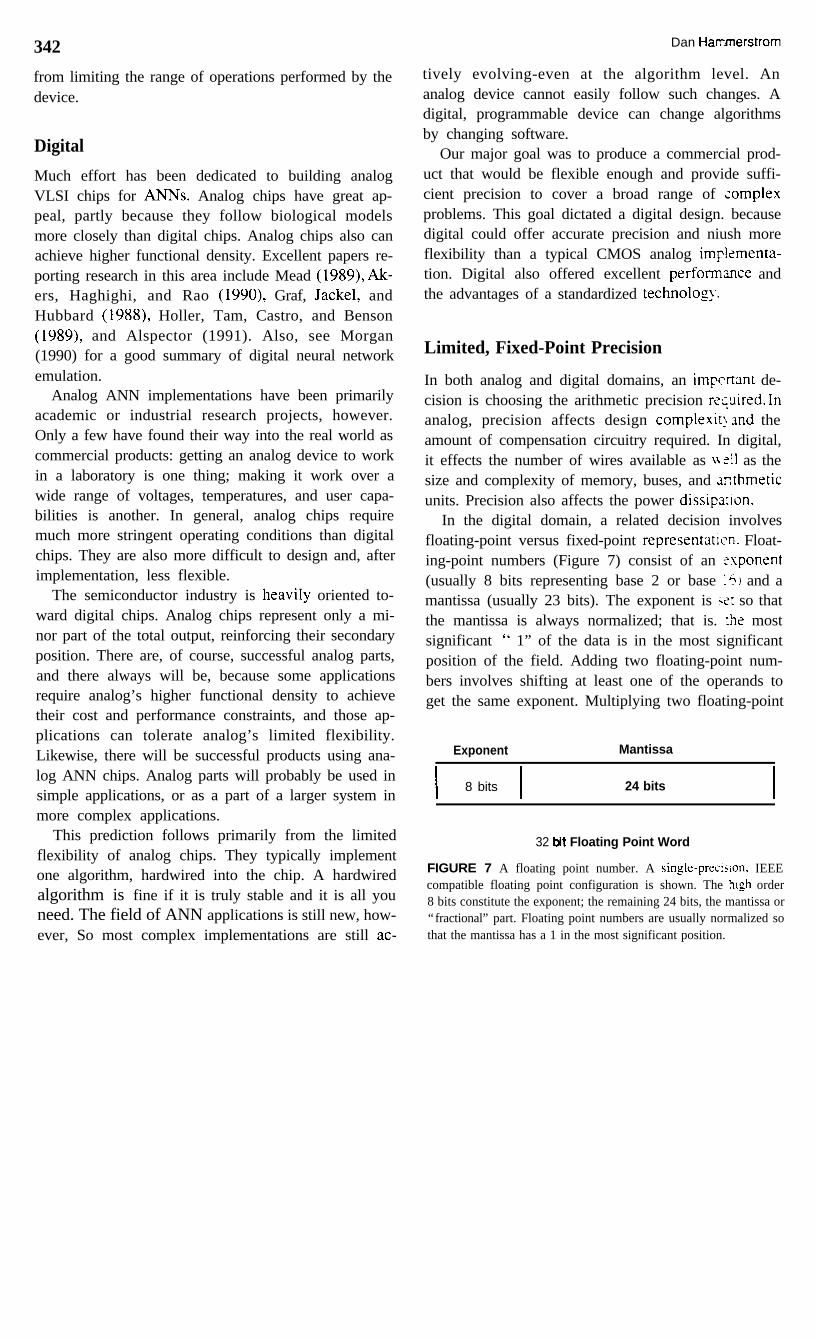
In the digital domain, a related decision involvesfloating-point versus fixed-point representaric’n. Float-ing-point numbers (Figure 7) consist of an _=uponent(usually 8 bits representing base 2 or base ;6~ and amantissa (usually 23 bits). The exponent is 5s: so thatthe mantissa is always normalized; that is. :he mostsignificant “ 1” of the data is in the most significantposition of the field. Adding two floating-point num-bers involves shifting at least one of the operands toget the same exponent. Multiplying two floating-point
Exponent Mantissa
I 8 bits I24 bits
I
32 tit Floating Point Word
FIGURE 7 A floating point number. A single-preckon. IEEEcompatible floating point configuration is shown. The high order8 bits constitute the exponent; the remaining 24 bits, the mantissa or“fractional” part. Floating point numbers are usually normalized sothat the mantissa has a 1 in the most significant position.
17. Digita’ VLSI Architecture for Real-World Problems 343numbers involves separate arithmetic on both expo-nents and mantissas. Both operations require postnor-malizing shifts after the arithmetic operations.
Floating point has several advantages. The primaryadvantage is dynamic range, which results from theseparate exponent. Another is precision, due to the 24-bit mantissas. The disadvantage to floating point is itscost in silicon area. Much circuitry is required to keeptrack of both exponents and mantissas and to performpre- and postoperation shifting of the mantissa. Thiscircuitr! is particularly complicated if high speed isrequired.
Fixed-point numbers consist of a numeral (usually16 to 1’ bits) and a radix point (in base 2, the binarypoint 1. In fixed point, the programmer chooses the po-sition of the radix point. This position is typically fixedfor the <alculation, although it is possible to changethe radix point under software control by explicitlyshifting operands. For many applications needing onlylimited dynamic range and precision, fixed point issufficient. It is also much cheaper than floating pointbecaus? it requires less silicon area.
After choosing a digital signal representation forCNAPS. the next question was how to represent thenumbers. Biological neurons are known to use rela-tive]!. i?w precision and to have a limited dynamicrange. These characteristics strongly suggest that adigital computer for emulating ANN structures shouldbe able to employ limited precision fixed-point arith-metic. This conjecture in turn suggests an opportunityto simplify significantly the arithmetic units and toprovid? greater computational density. Fixed-point ar-ithmetic also places the design near the desired pointon the flexibility versus performance/cost curve (Fig-ure 6).
To confirm the supposition that fixed point is ade-quate. we performed extensive simulations. We foundthat for the target applications, 8- or 16-bit fixed-pointprecision was sufficient (Baker & Hammerstrom,1989). Other researchers have since reached the sameconclusion (Hoehfeld and Fahlman, 1992; Shoemaker,Carlin. 6: Shimabukuro, 1990). In keeping with exper-imental results, we used a general 16-bit resolutioninside the PN. One exception was to use a 32-bit adder
to provide additional head-room for repeated multiply-accumulates. Another was to use 8-bit input and outputdata buses, because most computations involve 8-bitdata and 8- or 16-bit weights, and because busing ex-ternal to the PN is expensive in silicon area.
SIMD
The next major decision was how to control the PNs.A computer can have one or more instruction streamsand one or more data streams. Most computers aresingle instruction, single data (SISD) computers.These have one control unit and one processor unit,usually combined on one chip (a microprocessor). Thecontrol unit fetches instructions from program mem-ory and decodes them. It then sends data operationssuch as add, subtract, or multiply to the processingunit. Sequencing operations, such as branch, are exe-cuted by the control unit itself. The SISD computersare serial, not parallel.
Two major families of parallel computer architec-tures have evolved: multiple instruction, multiple data(MIMD) and single instruction, multiple data (SIMD).MIMD computers have many processing units, eachof which has its own control unit. Each control/processing unit can operate in parallel, executing manyinstructions at once. Because the processors operateindependently, MIMD is the most powerful and flexi-ble parallel architecture. The independent, asynchro-nous processors also make MIMD the most difficult touse, requiring complex processor synchronization.
The SIMD computers have many processors butonly one instruction stream. All processors receive thesame instruction at the same time, but each acts on itsown slice of the data. SIMD computers thus have anarray of processors and can perform an operation on ablock of data in one step. SIMD computing is oftencalled “data parallel” computing, because it appliesone control thread to multiple local data elements, ex-ecuting one instruction at each clock.
SIMD computation is perfect for vector and matrixarithmetic. Because of Amdahl’s law, however, SIMDis cost-effective only if most operations are matrix orvector operations. For general-purpose computing,

344this is not the case. Consequently, SIMD machines arepoor general-purpose computers and rarer than SISDor even MIMD computers. Our target domain is notgeneral-purpose computing, however. For ANNs andother image and signal processing algorithms, thedominant calculations are vector or matrix operations.SIMD fits this domain perfectly.
The SIMD architecture is a good choice for practicalreasons, too. One advantage is cost: SIMD is muchcheaper than MIMD, because there is only one controlunit for the entire array of processors. Another is thatSIMD is easier to program than MIMD, because allprocessors do the same thing at the same time. Like-wise, it is easier to develop computer languages forSIMD, because it is relatively easy to develop paralleldata structures where the data are operated on simul-taneously. Figure 8 shows a simple CNAPS-C pro-gram that multiplies a vector times a matrix. Normally,vector matrix multiply takes n* operations. By placing
Dan Hmmerstrom
# define N 20
#define K 30
typedef scaled 8 8 arithType;
domain Krows
{arithType sourceMatrix[N];
arithType resultVector;} dimK[K];
main0
{ int n;
[domain dimK].(
resultvector = 0;
for (n=O; n c N; n++)
resultvector += sourceMatrix[n] l getchar();
]
FIGURE 8 A CNAPS-C program to do a simple vector-matrixmultiply. The “data-parallel” programming is evident here. Withinthe loop, it is assumed because of the domain declaration that thereare multiple copies of each matrix element, one on each PN. Theprogram takes N loop iterations, which would require Nz on a se-quential machine.
each column of the matrix on each PN, it takes n op-erations on n processors.
In sum, SIMD was better than MIMD for CNAPSbecause it fit the problem domain, was much moreeconomical, and easier to program.
Broadcast Interconnect
The next decision concerned how to interconnect thePNs for data transfer, both within the arra! 3nd out-side it. Computer architects have develops2 severalinterconnect structures for connecting proczrsors inmultiprocessor systems. Because CNAPS is 1 SIMDmachine, we were interested only in sync:hronousstructures.
The two families of interconnect structure- me localand global. Local interconnect attaches onl! zzighbor-ing PNs. The most common local scheme :s NEWS(North-East-West-South, Figure 9). In NEWS. :he PNsare laid out in a two-dimensional array, and ?xh PNis connected to its four nearest neighbors. A one-
FIGURE 9 A two-dimensional PN layout. This cont;uration isoften called a “NEWS” network, because each PN corrects to itsnorth, east, west, and south neighbor. These networks pi?vide moreflexible intercommunication than a one-dimensional ~~.voork, butare more expensive to implement in VLSI and diffic2 to makework when redundant PNs are used.
17. Digita VLSI Architecture for Real-World Problems 345
dimensional variation connects each PN only to its leftand right neighbors.
Global interconnect permits any PN to talk to anyother PN. not just to .its immediate neighbors. Thereare several possible configurations with different lev-els of performance/cost. At one end of the scale, CTOSS-bar interconnect is versatile because it permits randompoint-to-point communications, but expensive [thecost is O!n’), where n is the number of PNs]. At theother end. hroadcasr interconnect is cheaper but lessflexible. Here, one bus connects all PNs, so any onePN can talk to any other (or set of others) in one clock.On the other hand, it takes n clocks for all PNs to havea turn. The cost is O(1). In between crossbar andbroadcast are other configurations that can emulate across-bar in O(logn) clocks and have cost O(nlogn).
Choosing an interconnect structure interacted withother design choices. We decided against using a sq’s-folio computing style. in which operands, intermediateresults. or both flow down a row of PNs using onlylocal inrer<onnect. Systolic arrays are harder to pro-gram. Thz>’ are also occasionally inefficient becauseof the cl<~ks needed to fill or empty the pipeline-peak effi%rcy occurs only when all PNs see all oper-ands. Chcoosing a systolic array would have permittedus to us= local interconnect, saving cost. Decidingagainst i: forced us to provide some form of globalinterconn23.
Choosing “global” leads to the next choice: whattype? Th: basic computations in our target applica-tions required “one-to-many” or “many-to-many”communization almost exclusively. We therefore de-cided to use a broadcast bus, which uses only oneclock for one-to-many communication. In the many-to-many’ zse, n PNs can talk to all y1 PNs in y1 clocks.Broadcast interconnect thus allows y2* connections in y2clocks. Such O(n2) total connectivity occurs often inour apph<arions. An example is a back-propagationnetwork in which all nodes in one layer connect to allnodes in the next.
Another advantage is that broadcast interconnectionis synchronous and fits the synchronous SIMD struc-:ure quite well. We were able to use a “slotted” pro-:ocol, in lvhich each connection occurs at a known
time on the bus. Because the time is known, there isno need to send an address with each data element,saving wires, clocks, or both. Also, the weight addressunit can “remember” the slot number and use it toaddress the weight associated with the connection.A single broadcast bus is simple, economical to im-plement, and efficient for the application domain. Infact, if every PN always communicates with everyother PN, then broadcast offers the best possibleperformance/cost.
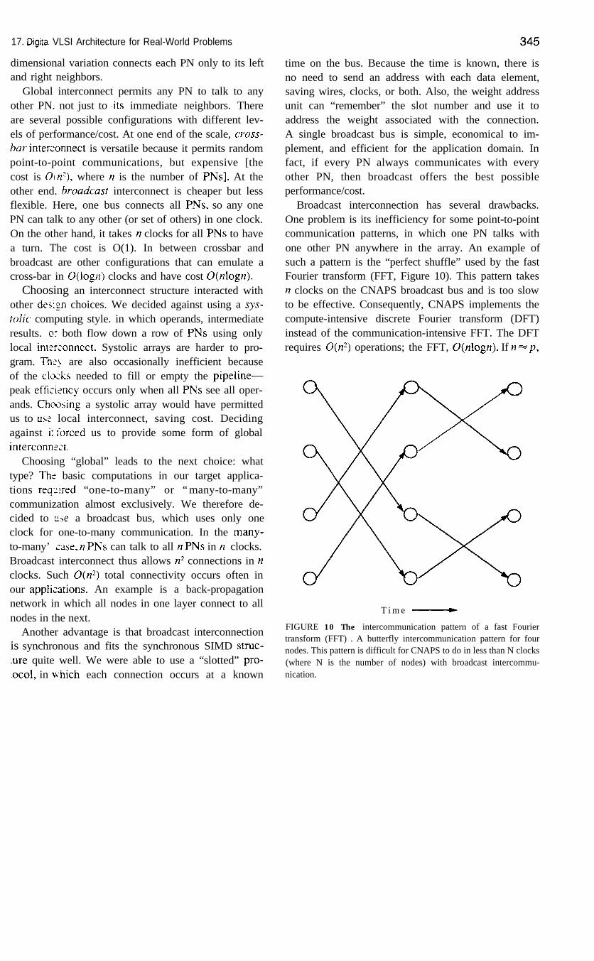
Broadcast interconnection has several drawbacks.One problem is its inefficiency for some point-to-pointcommunication patterns, in which one PN talks withone other PN anywhere in the array. An example ofsuch a pattern is the “perfect shuffle” used by the fastFourier transform (FFT, Figure 10). This pattern takesn clocks on the CNAPS broadcast bus and is too slowto be effective. Consequently, CNAPS implements thecompute-intensive discrete Fourier transform (DFT)instead of the communication-intensive FFT. The DFTrequires O(n*) operations; the FFT, O(nlogn). If n = p,
T i m e -
FIGURE 10 The intercommunication pattern of a fast Fouriertransform (FFT) . A butterfly intercommunication pattern for fournodes. This pattern is difficult for CNAPS to do in less than N clocks(where N is the number of nodes) with broadcast intercommu-nication.
346 Dan Hammerstrom
where p is the number of PNs, then CNAPS can per-form a DFT in O(n) clocks. If n > p, then performancecan approach the O(nlogn) of a sequential processor.
Another problem involves computation localized ina portion of an input vector, where each PN operateson a different (possibly overlapping) subset of the el-ements. Here, all PNs must wait for all inputs to bebroadcast before any computation can begin. A com-mon example of this situation is the limited receptivefield structure, often found in image classificationand character recognition networks. The convolutionoperation, also common in image processing, usessimilar localized computation. The convolution canproceed rapidly after some portion of the image hasbeen input into each PN, because each PN operatesindependently on its subset of the image.
When these subfields overlap (such as is in convo-lution), a PN must communicate with its neighbors. Toimprove performance for such cases, we added a one-dimensional inter-PN pathway, connecting each PN toits right and left neighbors. (One dimension was cho-sen over two to allow processor redundancy, discussedlater). The CNAPS array therefore has both global(broadcast) and local (inter-PN) interconnection. Anexample of using the inter-PN pathway might be im-age processing, where a column of each image is allo-cated to each PN. The inter-PN pathway permitsefficient communication between columns-and,consequently, efficient computation for most image-processing algorithms.
A final problem is sparse random interconnect,where each node connects to some random subset ofother nodes. Broadcast, from the viewpoint of the con-nected PNs, is in this case efficient. Nonetheless, whena slotted protocol is used, many PNs are idle becausethey lack weights connected to the current input anddo not need the data being broadcast. Sparse intercon-nect affects all aspects of the architecture, not just datacommunication. To improve efficiency for sparselyconnected networks, the CNAPS PN offers a specialmemory technique called virtual zero, which savesmemory locations that would otherwise be filled withzeros by not loading zeros into memory for unused
connections. The Virtual Zero technique does not helpthe idle PN problem, however. Full efficiency withsparse interconnect requires a much more complex ar-chitecture, including more individualized control perPN, more complex memory-referencing capabilities,and so on, and is beyond the scope of this chapter.
On-Chip Memory
One of the most difficult decisions was whether toplace the local memory on-chip inside the PN or off-chip. Both approaches have advantages and draw-backs-it was a complex decision with no obviousright answer and little opportunity for compromise.
The major advantage of off-chip memory is that itallows essentially unlimited memory per PN. Placingmemory inside the PN, in contrast, limits the availablememory because memory takes significant siliconarea. Increasing PN size also limits the number of PNs.Another advantage to off-chip memory is that it allowsthe use of relatively low-cost commercial memorychips. On-chip memory, in contrast, increases the costper bit-even if the memory employs a commercialmemory cell.
The major advantage of on-chip memory is that itallows much higher bandwidth for memory access. Tosee that bandwidth is a crucial factor, consider the fol-lowing analysis. Recall that each PN has its on-n dataarithmetic units, therefore each PN requires a uniquememory data stream. The CNAPS-1064 has 61 PNs,each potentially requiring up to 2 bytes per clock. At25 MHz, that is 25M * 64 * 2 = 3.2 billion by-tss/sec.Attaining 3.2 billion bytes/set from off-chip memoryis difficult and expensive because of the limits on thenumber of pins per chip and the data rate per pin.’ Anoption would be to reduce the number of PNs per chip,eroding the benefit of maximum parallelism.
Another advantage to on-chip memory is that eachPN can address different locations in memory in each
‘For most implementations, the bit rate per pin is roughly equalto the clock rate, which can vary anywhere from 25 to 700 MHZ.There are some special interface protocols which now allow up to500 Mbitdsec per pin.

17. Digital VLSI Architecture for Real-World Problems
clock. Systems with off-chip memory, in contrast, typ-ically require all PNs to address the same location foreach memory reference to reduce the number of exter-nal output pins for memory addressing. With a sharedaddress only a single set of address pins is required foran entire PN array. Allowing each PN to have uniquememory addresses, requires a set of address pins foreach PN. which is expensive. Yet, having each PNaddress its own local memory improves versatility andspeed, because table lookup, string operations, andother kinds of “indirect” reference are possible.
Another advantage is that the total system is simpler.On-chip memory makes it possible to create a com-plete system with little more than one sequencer chip,one PN array chip, and some external RAM or ROMfor the sequencer program. (Program memory needsless bandwidth than PN memory because SIMD ma-chines access it serially, one instruction per clock.)
It is possible to place a cache in each PN, then useoff-chip memory as a backing store, which attempts togain the benefits of both on-chip and off-chip memoryby using aspects of both designs. Our simulations onthis point verified what most people who work inANNs already suspected: Caching is ineffective forANNs because of the nonlocality of the memory ref-erence streams. Caches are effective if the processorrepeatedi! accesses a small set of memory locations,called a il.orking set. Pattern recognition and signalprocessing programs rarely exhibit that kind of behav-ior: instead. they reference long, sequential vectorarrays.
Separate PN memory addressing also reduces thebenefit of caching. Unless all PNs refer to the sameaddress. some PNs can have a cache miss and othersnot. If the probability of a cache miss is 10% per PN,then a 25PN array will most likely have a cache missevery clock. But because of the synchronous SIMDcontrol, all PNs must wait for the one or more PNs thatmiss the cache. This behavior renders the cache use-less. A MI54D structure overcomes the problem, butincreases system complexity and cost.
As this discussion suggests, local PN memory is acomplex topic with no easy answers. Primarily be-
347
cause of the bandwidth needs and because we had ac-cess to a commercial density static RAM CMOSprocess, we decided to implement PN memory onchip, inside the PN. Each PN has 4 KB of static RAMin the current 1064 and 1016 chips.
CNAPS is the only architecture for ANN applica-tions we are aware of that uses on-chip memory. Sev-eral designs have been proposed that use off-chipmem-ory. The CNS system being developed at Berke-ley (Wawrzyneck, Asanovic, & Morgan, 1993), forinstance, restricts the number of PNs to 16 per chip. Italso uses a special high-speed PN-to-memory bus toachieve the necessary bandwidth. Another system, de-veloped by Ramacher at Siemens (Ramacher et al.,1993) uses a special systolic pipeline that reduces thenumber of fetches required by forcing each memoryfetch to be used several times. This organization isefficient at doing inner products, but has restrictedflexibility. HNC has also created a SIMD array calledthe SNAP (Means & Lisenbee, 1991). It uses floating-point arithmetic, reducing the number of PNs on achip to only four-in turn, reducing the bandwidthrequirements.
The major problem with on-chip memory is its lim-ited memory capacity. Although this limitation doesrestrict CNAPS applications somewhat, it has notbeen a major problem. With early applications, theperformance/cost advantages of on-chip memory havebeen more important than the memory capacity limits.
Redundancy for Yield Improvement
During the manufacture of integrated circuits, smalldefects and other anomalies occur, causing some cir-cuits to malfunction. These defects have a more or lessrandom distribution on a silicon wafer. The larger thechip, the greater the probability that at least one defectwill occur there during manufacturing. The number ofgood chips per wafer is called the yield. As chips getlarger, fewer chips fit on a wafer and more have de-fects, therefore, yield drops off rapidly with size. Be-cause wafer costs are fixed, cost per chip is directlyrelated to the number of good chips per wafer. The
348 Dan Hammerstrom
result is that bigger chips cost more. On the other hand,bigger chips do more, and their ability to fit more func-tion into a smaller system makes big chips worth more.Semiconductor engineers are constantly pushing thelimits to maximize both function and yield at the sametime.
One way to build larger chips and maximize yieldis to use redundancy, where many copies of a circuitare built into the chip. After fabrication, defective cir-cuits are switched out and replaced with a good copy.Memory designers have used redundancy for years;where extra memory words are fabricated on the chipand substituted for defective words. With redundancy,some defects can be tolerated and still yield a fullyfunctional chip.
One advantage of building ANN silicon is that eachPN can be simple and small. In the CNAPS processorarray chip, the PNs are small enough to be effective as“units of redundancy.” By fabricating spare PNs, wecan significantly improve yield and reduce cost perPN. The 1064 has 80 PNs (in an 8 X 10 array), andthe 1016 has 20 (4 X 5). Even with a relatively highdefect density, the probability of at least 64 out of 80(or 16 out of 20) PNs being fully functional is close to1 .O. CNAPS is the first commercial processor to makeextensive use of such redundancy to reduce costs.Without redundancy, the processor array chips wouldhave been smaller and less cost-effective. We estimatea CNAPS implementation using redundancy has abouta two-times performance/cost advantage over onelacking redundancy.
Redundancy also influenced the decision to use lim-ited-precision, fixed-point arithmetic. Our analysesshowed that floating-point PNs would have been toolarge to leverage redundancy; hence, floating pointwould have been even more expensive than just thesize difference (normally about a factor of four) indi-cates. Redundancy also influenced the decision to useone-dimensional inter-PN interconnect. One-dimen-sional interconnect makes it relatively easy to imple-ment PN redundancy, because any 64 of the 80 PNscan be used. Two-dimensional interconnect compli-cates redundancy and was not essential for our appli-cations. We chose one-dimensional interconnect, be-
cause it was adequate for our applications and does notimpact the PN redundancy mechanisms.
Limitations
In retrospect, we are satisfied with the decisions madein designing the CNAPS architecture. We have no re-grets about the major decisions such as the choices ofdigital, SIMD, limited fixed point. broadcast intsrcon-nect, and on-chip memory.
The architecture does have a few minor bonlsnecksthat will be alleviated in future versions. For example.the g-bit input/output buses should be 16-bit. In linewith that, a true one-clock 16 X 16 multiply is needed.as well as better support for rounding. And future ver-sions will have higher frequencies and more pn-chipmemory. The one-dimensional inter-PN bus is 3. bits.it should be 16 bits. Despite these few limitaricns. thearchitecture has been successfully applied to rsveralapplications with excellent performance.
Product Realization and Software
Adaptive Solutions has created a complete dsk-clap-ment software package for CNAPS. It includss a li-brary of important ANN algorithms and a C compilerwith a library of commonly used functions.’ Severalboard products are now available and sold to custom-ers to use for ANN emulation, image and signal pro-cessing, and pattern recognition applications.
CNAPS APPLICATIONS
This section reviews several CNAPS applications. Be-cause of the nature of this book its focus is on XNXapplications, although CNAPS has also been used fornon-ANN applications such as image processing.Some applications mix ANN and non-ANS tech-niques. For example, an application could preprocessand enhance an image via standard imaging algo-
*CNAPS-C is a data parallel version of the standard C lqua~s.
17. Digital VLSI Architecture for Real-World Problems 349
most curve-fitting problems, such as function predic-tion, which have more stringent accuracy require-ments. In those cases in which BP16 does not have theaccuracy of floating point, BP32 is as accurate as float-ing point in all cases studied so far. The rest of thissection focuses on the BP16 algorithm. It does notdiscuss the techniques involved in dealing with limitedprecision on CNAPS.
Back-propagation has two phases. The first is feed-forward operation, in which the network passes datawithout updating weights. The second is error back-propagation and weight update during training. Eachphase will be discussed separately. This discussion as-sumes that the reader already has a working under-standing of BP
rithms. then use an ANN classifier on segments of theimage. keeping all data inside the CNAPS array for alloperations.9 A discussion of the full range of CNAPS’scapabilities is beyond the scope of this paper. For adetailed discussion of CNAPS in signal processing,see Skinner, 1994.
Back-Propagation
The most popular ANN algorithm is back-propagation(BP; Rumelhart & McClellan, 1986). Although itrequires large computational resources during training,BP has several advantages that make it a valuablealgorithm:
l it is reasonably generic, meaning that one networkmodel (emulation program) can be applied to a widerange of applications with little or no modification;
l its nonlinear, multilayer architecture lets it solvecomplex problems:
l it is relatively easy to use and understand; andl several commercial software vendors have excellent
BP implementations.
It is estimated that more than 90% of the ANN ap-plications in use today use BP or some variant of it.We therefore felt that it was important for CNAPS toexecute BP efficiently. This section briefly discussesthe general implementation of BP on CNAPS. Formore detail, see McCartor (1991).
There are two CNAPS implementations of BP asingle-precision version (BP1 6) and a double-preci-sion version (BP32). BP16 uses unsigned g-bit inputand output values and signed 16-bit weights. The ac-tivation function is a traditional sigmoid, implementedby table lookup. BP32 uses signed 16-bit input andoutput values and signed 32-bit weights. The activa-tion function is a hyperbolic tangent implemented bytable lookup for the upper 8 bits and by linear extrap-olation for the lower 8 bits. All values are fixed point.We have found that BP16 is sufficient for all classifi-zation problems. BP16 has also been sufficient for
9To change algorithms. the CSC need only branch to a differentsection of a program.
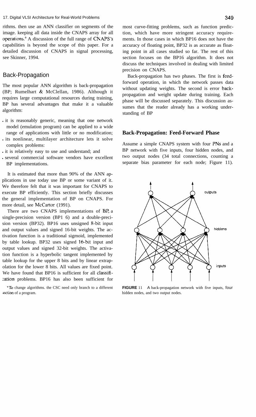
Back-Propagation: Feed-Forward Phase
Assume a simple CNAPS system with four PNs and aBP network with five inputs, four hidden nodes, andtwo output nodes (34 total connections, counting aseparate bias parameter for each node; Figure 11).
FIGURE 11 A back-propagation network with five inputs, fourhidden nodes, and two output nodes.

350Allocate nodes 0 and 4 to PNO, nodes 1 and 5 to PN 1,node 2 to PN2, and node 3 to PN3. When a node isallocated to a PN, the local memory of that PN isloaded with the weight values for each of the node’sconnections and with the lookup table for the sig-moid function. If learning is to be performed, theneach connection requires a 2-byte weight plus 2 bytesto sum the weight deltas, and a 2-byte transposeweight (discussed below). This network then requires204 bytes for connection information. Using momen-tum-ignored here for simplicity-would requiremore bytes per connection.
Each input vector contains five elements. Theweight index notation is WA,,, where A is the layerindex, in our example, 0 for input, 1 for hidden, and 2for output. B indexes the node in the layer, and C in-dexes the weight in the node. To start the emulationprocess, each element of the input vector is read froman external file by the CSC and broadcast over theInbus to all four PNs. PNO performs the multiply v0 *~1,; PNl, v0 * wl,,; and so on. This happens in oneclock. In the next clock, v, is broadcast, PNO computesVI * wl,,; PNl, v, * WI,,; and so on. Meanwhile, theprevious clock’s products are sent to the adder, whichinitially contains zero.
All of the hidden-layer products have been gener-ated after five clocks. One more clock is required toadd the last product to the accumulating sum (ignoringthe bias terms here for simplicity). Next, all PNs ex-tract the most significant byte out of the product anduse it as an address into the lookup table to get thesigmoid output. The read value then is put into the out-put buffer, and the PNs are ready to compute the outputnode outputs.
The next step is computing the output-layer nodevalues (nodes 4 and 5). In the first clock, PNO trans-mits its output (node O’s output) onto the output bus.This value goes through the CSC and comes out on theInbus, where it is broadcast to all PNs. Although onlyIWO and PNl are used, all PNs compute values (PN2and PN3 compute dummy values). PNO and PN 1 com-pute n, * ~2, and n, * w2,,. In the next clock, nodel’s value is broadcast and n, * w2,, and n, * w2,, arecomputed, and so on. After four clocks, PNO and PNl
Dan Hammerstrom
have computed all products. One more clock is neededfor the last addition; then, a sigmoid table lookup isperformed. Finally, the node 4 and 5 outputs are trans-mitted sequentially on the Outbus, and the CSC writesthem into a file.
Let a connection clock be the time it takes to com-pute one connection. For standard BP a connectionrequires a multiply-accumulate plus, depending on thearchitecture, a memory fetch of the next weight, thecomputation of that weight’s address, and so on. Forthe CNAPS PN, a connection clock takes one cycle.On a commercial microprocessor chip, a connectionclock can require one or more cycles, because manycommercial chips cannot simultaneously execute alloperations required to compute a connection clock:weight fetch, weight address increment, input elementfetch, multiply, and accumulate. These operations cantake up to 10 clocks on many microprocessors. Muchof this overhead is memory fetching, because manystate-of-the-art microprocessors are making more useof several levels of intermediate data caching. How-ever, as discussed previously, ANNs are notoriouscache busters, so many memory and input elementfetches can take several clocks each.
Simulating a three-layer BP network with .f’. inputs,NH nodes in the hidden layer, and N, nodes in theoutput layer will require (N, * NH) * (N, * _\.,) + N,connection clocks for nonlearning, feed-foru-ard op-eration on a single-processor system. On CS.\PS. as-suming there are more PNs than hidden or outputnodes, the same network will require N, + _\e.q + N,connection clocks. For example, assume that N, =256, NH = 128, and N, = 64. For a single processorsystem, the total is 73,792 connection clocks: forCNAPS, 448. If a workstation takes about four cycleson average per connection, which is typical. to com-pute a connection, then CNAPS is about 600X fasteron this network.
Back-Propagation: Learning Phase
The second and more complex aspect of BP learningis computing the weight delta for each connection. Adetailed discussion of this computation and its CNAPS

17. Digital VLSI Architecture for Real-World Problems 351implementation is beyond the scope of this chapter, soonly a brief overview is given here. The computationis more or less the same as a sequential implementa-tion. The basic learning operation in BP is to computean error signal for each node. The error signal is pro-portional to that node’s contribution to the output error(the difference between the target output vector andthe actual output error). From the error signal, a nodecan then compute how to update its weights. At theoutput layer, the error signal is the difference betweenthe feed-forward output vector and the target outputvector for that training vector. The output nodes cancompute their error signals in parallel.
The next step is to compute the delta for each outputnode’s input weight (the hidden-to-output weights).This computation can be done in parallel, with eachnode computing, sequentially, the deltas for allweights of the output node on this PN. If a batchingalgorithm is used, then the deltas are added to a dataelement associated with each weight. After severalweight updates have been computed, the weights areupdated according to an accumulated delta.
The next step is to compute the error signals forthe hidden-layer nodes, which requires a multiply-accumulate of the output-node error signals throughthe output-node weights. Unfortunately, the output-layer w.eights are in the wrong place (on the outputPNs) for computing the hidden-layer errors; that is, thebidder, nodes need weights that are scattered amongthe output PNs, which can best be represented as atranspose of the weight matrix for that layer. In otherwords. a row of the forward weight matrix is allo-cated to each PN. When propagating the error back tothe hidden layer, the inner product uses the columnof the same matrix which is spread across PNs. Atranspose of the weight matrix makes these columnsinto rows and allows efficient matrix-vector opera-tions, A transpose operation is slow on CNAPS, tak-ing 0(h3) operations. The easiest solution was tomaintain two weight matrices for each layer, the feed-forward version and a transposed version for the er-ror back-propagation. This requires twice the weightmemory for each hidden node, but permits error prop-agation to be parallel, not serial. Although the new
weight value need only be computed once, it mustbe written to two places. This duplicate transposeweight matrix is required only if learning is to beperformed.
After the hidden-layer error signals have been com-puted, the weight delta computation can proceed ex-actly as previously described. If more than one hiddenlayer is used, then the entire process is repeated for thesecond hidden layer. The input layer does not requirethe error signal.
For nonbatched weight update, in which the weightsare updated after the presentation of each vector, thelearning overhead requires about five times more cy-cles than feed-forward execution. A 256-PN (four-chip) system with all PNs busy can update about onebillion connections per second, almost one thousandtimes faster than a Sparc2 workstation. A BP networkthat takes an hour on a Sparc2 takes only a few secondson CNAPS.
Simple Image ProcessingOne major goal of CNAPS was flexibility because, byAmdahl’s law, the more the problem can be parallel-ized the better; therefore, other parallelizable, but non-ANN, parts of the problem Should also be moved toCNAPS where possible. Many imaging applications,including OCR programs, require image processingbefore turning the ANN classifier loose on the data. Acommon image-processing operation is convolutionby spatial filtering.
Using spatial (pixel) filters to enhance an image re-quires more complex computations than simple pixeloperations require. Convolution, for example, is acommon operation performed during feature extrac-tion to filter noise or define edges. Here, a kernel, anM by M dimensional matrix, is convolved over an im-age. In the following equation, for instance, the localkernel k is convolved over an N by N image a to pro-duce a filtered N by N image b:
6, = C kp.qar - *., - qP.4
(i I i,j i N)(l ‘p,q 5 M)
(2)
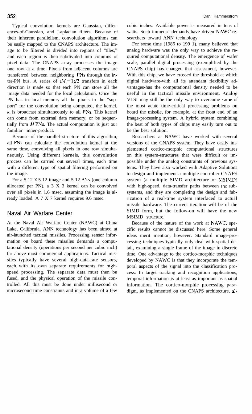
352 Dan Hammerstrom
Typical convolution kernels are Gaussian, differ-ences-of-Gaussian, and Laplacian filters. Because oftheir inherent parallelism, convolution algorithms canbe easily mapped to the CNAPS architecture. The im-age to be filtered is divided into regions of “tiles,”and each region is then subdivided into columns ofpixel data. The CNAPS array processes the imageone row at a time. Pixels from adjacent columns aretransferred between neighboring PNs through the in-ter-PN bus. A series of (M - 1)/2 transfers in eachdirection is made so that each PN can store all theimage data needed for the local calculation. Once thePN has in local memory all the pixels in the “sup-port” for the convolution being computed, the kernel,k, is broadcast simultaneously to all PNs. This kernelcan come from external data memory, or be sequen-tially from M PNs. The actual computation is just ourfamiliar inner-product.
Because of the parallel structure of this algorithm,all PNs can calculate the convolution kernel at thesame time, convolving all pixels in one row simulta-neously. Using different kernels, this convolutionprocess can be carried out several times, each timewith a different type of spatial filtering performed onthe image.
For a 5 12 X 5 12 image and 5 12 PNs (one columnallocated per PN), a 3 X 3 kernel can be convolvedover all pixels in 1.6 msec, assuming the image is al-ready loaded. A 7 X 7 kernel requires 9.6 msec.
Naval Air Warfare CenterAt the Naval Air Warfare Center (NAWC) at ChinaLake, California, ANN technology has been aimed atair-launched tactical missiles. Processing sensor infor-mation on board these missiles demands a compu-tational density (operations per second per cubic inch)far above most commercial applications. Tactical mis-siles typically have several high-data-rate sensors,each with its own separate requirements for high-speed processing. The separate data must then befused, and the physical operation of the missile con-trolled. All this must be done under millisecond ormicrosecond time constraints and in a volume of a few
cubic inches. Available power is measured in tens ofwatts. Such immense demands have driven N‘\WC re-searchers toward ANN technology.
For some time (1986 to 199 1). many believed thatanalog hardware was the only way to achieve the re-quired computational density. The emergence of waferscale, parallel digital processing (exemplified by theCNAPS chip) has changed that assessment, however.With this chip, we have crossed the threshold at whichdigital hardware-with all its attendant flexibility ad-vantages-has the computational density needed to beuseful in the tactical missile environment. .\nalogVLSI may still be the only way to overcome some ofthe most acute time-critical processing problems onboard the missile, for example. at the front end of animage-processing system. A hybrid system combiningthe best of both types of chips may easily turn out tobe the best solution.
Researchers at NAWC have worked with severalversions of the CNAPS system. They have easily im-plemented cortico-morphic computational structureson this system-structures that were difficult or im-possible under the analog constraints of previous sys-tems. They have also worked with Adaptive Solutionsto design and implement a multiple-controller CYAPSsystem (a multiple SIMD architecture or h1SIMD)with high-speed, data-transfer paths between the sub-systems, and they are completing the design and fab-rication of a real-time system interfaced to actualmissile hardware. The current iteration will be of theSIMD form, but the follow-on will have the newMSIMD structure.
Because of the nature of the work at NAW-C. spe-cific results cannot be discussed here. Some generalideas merit mention, however. Standard image-pro-cessing techniques typically only deal with spatial de-tail, examining a single frame of the image in discretetime. One advantage to the cortico-morphic techniquesdeveloped by NAWC is that they incorporate the tem-poral aspects of the signal into the classification pro-cess. In target tracking and recognition applications,temporal information is at least as important as spatialinformation. The cortico-morphic processing para-digm, as implemented on the CNAPS architecture, al-
17. Digital VLSI Architecture for Real-World Problems 353
lows sequential processing of patches of data in realtime. similar to the processing in the vertebrate retinaand cortex.
One important near-term application of this compu-tational structure is in the area of adaptive, nonuni-formity compensation for staring focal plane arrays. Itappears also that this structure will allow the imple-mentation of three-dimensional wavelet transformswhere the third dimension is time.
Lynch/Granger PyriformImplementation
Researchers Gary Lynch and Richard Granger (Grangeret al.. this volume) at the University of California,Irvin?. have produced an ANN model based on theirstudies of the pyriform cortex of the rat. The algo-rithm contains features abstracted from actual bio-logical operations. and has been implemented on theCNAPS parallel computer (Means & Hammerstrom,1991 I.
Ths algorithm contains both parallel and serial ele-ments. and lends itself well to execution on CNAPS.Clusters of competing neurons, called patches or sub-r?ers. hierarchically classify inputs by first competingfor the greatest activation within each patch, then sub-tracting the most prominent features from the input asit procseds down the lateral olfactory tract (LOT, theprimar>- input channel) to subsequent patches. Patchacti\larion and competition occur in parallel in theCNAPS implementation. A renormalization functionanalogous to the automatic gain control performed inpyriform cortex also occurs in parallel across compet-ing PNs in the CNAPS array.
Transmission of LOT input from patch to patch isan inherently serial element of the pyriform model, soopportunities for parallel execution for this part of themodel are few. Nevertheless, overall speedups for ex-ecution on CNAPS (compared to execution on a serialmachine) of 50 to 200 times are possible, dependingon network dimensions.
Refinements of the pyrifonn model and applica-tions of it to diverse pattern recognition applicationscontinue.
Sharp Kanji
Another application that has successfully used ANNsand the CNAPS system is a Kanji optical characterrecognition (OCR) system developed by the SharpCorporation of Japan. In OCR, a page of printed textis scanned to produce a bit pattern of the entire image.The OCR program’s task is to convert the bit patternof each character into a computer representation of thecharacter. In the United States and Europe, the mostcommon representation of Latin characters is the &bitASCII code. In Japan, because of their unique writingsystem, it is the 16-bit JIS code.
The OCR system requires a complex set of imagerecognition operations. Many companies have foundthat ANNs are effective for OCR because ANNs arepowerful classifiers. Many commercial OCR compa-nies, such as Caere, Calera, Expervision, and Mimet-its, use ANN classifiers as a part of their software.
Japanese OCR is much more difficult than EnglishOCR because Japanese has a larger character set. Writ-ten Japanese has two basic alphabets. The first isKanji, or pictorial characters borrowed from China.Japanese has tens of thousands of Kanji characters,although it is possible to manage reasonably well withabout 3500 characters. Sharp chose these basic Kanjicharacters for their recognizer.
The second alphabet is Kana, composed of two pho-netic alphabets (hiragana and katakana) having 53characters each. Typical written Japanese mixes Kanjiand Kana. Written Japanese also employs arabic nu-merals and Latin characters also found in business andnewspaper writing. A commercial OCR system mustbe able to identify all four types of characters. To addfurther complexity, any character can appear in severaldifferent fonts.
Japanese keyboards are difficult to use, so a muchsmaller proportion of business documentation thanone sees in the United States and other western coun-tries is in a computer readable form. This difficultycreates a great demand for the ability to read accu-rately printed Japanese text and to convert it to thecorresponding JIS code automatically. Unfortunately,because of the large alphabet, computer recognition of

354
written Japanese is a daunting task. At the time thischapter is being written, the commercial market con-sists of slow (10-50 characterslsec), expensive (tensof thousands of dollars), and marginally accurate(96%) systems. Providing high speed and accuracy fora reasonable price would be a quantum leap in capa-bility in the current market.
Sharp Corporation and Mitsubishi Electric Corpo-ration have both built prototype Japanese recognitionsystems based on the CNAPS architecture. Both sys-tems recognize a total of about 4000 characters in 15or more different fonts at accuracies of more than 99%and speeds of several hundred characters per second.These applications have not yet been released as com-mercial products, but both companies have announcedintentions to do so.
Sharp’s system uses a hierarchical three-layer net-work (Hammerstrom, 1993; Togawa, Ueda, Aramaki,& Tanaka, 199 1; Figures 12 and 13). Each layer isbased on the Kohonen’s Learning Vector Quantization(LVQ), a Bayesian approximation algorithm that shiftsthe node boundaries to maximize the number of cor-rect classifications. In Sharp’s system, unlike back-propagation, each hidden-layer node represents acharacter class, and some classes are assigned to sev-eral nodes. Ambiguous characters pass to the nextlayer. When any layer unambiguously classifies a char-acter, it has been identified, and the system moves onto the next character.
The first two levels take as input a 16 X 16 pixelimage (256 elements) (Figure 12). With some excep-tions, these layers classify the character into multiplesubcategories. The third level has a separate networkper subcategory (Figure 13). It uses a high-resolution32 X 32 pixel image (1024 elements), focusing on thesubareas of the image known to have the greatest dif-ferences among characters belonging to the subcate-gory. These subareas of the image are trained totolerate reasonable spatial shifting without sacrificingaccuracy. Such shift tolerance is essential because ofthe differences among fonts and shifting duringscanning.
Sharp’s engineers clustered 3303 characters into893 subcategories containing similar characters. The
Dan Hammerstrom
use of subcategories let Sharp build and train severalsmall networks instead of one large network. Eachsmall network took its input from several local recep-tive fields designed to look for particular features. Thelocations of these fields were chosen automaticallyduring training to maximize discriminative informa-tion. The target features are applied to several posi-tions within each receptive field, enhancing the shifttolerance of the field.
On a database of scanned characters that includedmore than 26 fonts, Sharp reported an accuracy of99.92% on the I3 fonts used for training and 99.01%accuracy on characters on the 13 fonts used for testing.These results show the generalization capabilities ofthis network.
NON-CNAPS APPLICATIONS
This section discusses two applications that do not useCNAPS (although they could easily use the CNAPSBP implementation).
x
Stage 1
FIGURE 12 A schematicized version of the three-layer LVQ net-work that Sharp uses in their Kanji OCR system. The character ispresented as a 16 X 16 or 256-element system. Some characters arerecognized immediately; others are merely grouped with similarcharacters.

17. Digital VLSI Architecture for Real-World Problems 355
FIGURE 13 Distinguishing members of a group by focusing on a group-specific subfield.Here. a more detailed 32 X 32 image is used (Togawa et al., 1991).
Nippon SteelANNs are starting to make a difference in process con-trol for manufacturing. In many commercial environ-ments, controlling a complex process can be beyondthe best adaptive control systems or rule-based expertsystems. One reason for this is that many natural pro-cesses are strongly nonlinear. Most adaptive controltheory, on the other hand, assumes linearity. Further-more, many processes are so complex that there is noconcise mathematical description of the process, justlarge amounts of data.
Working with such data is the province of ANNs,because they have been shown to extract, from data
alone, accurate descriptions of highly complex, non-linear processes. After the network describes the pro-cess, it can be used to help control it. Anothertechnique is to use two networks, where one modelsthe process to be controlled and the other the inversecontrol model. An inverse network takes as input thedesired state and returns the control values that placethe process in that state.
There are many examples of using ANNs for indus-trial process control. This section describes an appli-cation in the steel industry, developed jointly byFujitsu Ltd., Kawasaki, and Nippon Steel, Kitakyu-shu-shi, Japan. The technique is more effective than

356 Dan Hammerstrom
any previous technique and has reduced costs by sev-eral million dollars a year.
This system controls a steel production processcalled continuous casting. In this process, molten steelis poured into one end of a special mold, where themolded surface hardens into a solid shell around themolten center. Then, the partially cooled steel is pulledout the other end of the mold. Everything works fineunless the solid shell breaks, spilling molten steel andhalting the process. This “breakout” appears to becaused by abnormal temperature gradients in the mold,which develop when the shell tears inside the mold.The tear propagates down the mold toward a secondopening. When the tear reaches the open end, a break-out occurs. Because a tear allows molten metal totouch the surface of the mold, an incipient breakout isa moving hot spot on the mold. Such tears can bespotted by strategically placing temperature sensingdevices on the mold. Unfortunately, temperature fluc-tuation on the mold makes it difficult to find the hotspot associated with a tear. Fujitsu and Nippon Steeldeveloped an ANN application that recognizes break-out almost perfectly. It has two sets of networks: thefirst set looks for certain hot spot shapes; the second,for motion. Both were developed using the back-propagation algorithm.
The first type of network is trained to find a partic-ular temperature rise and fall between the input andoutput of the mold. Each sensor is sampled 10 times,providing 10 time-shifted inputs for each network for-ward pass. These networks identify potential breakoutprofiles. The second type of network is trained on ad-jacent pairs of mold input sensors. These data are sam-pled and shifted in six steps, providing six time-shiftedinputs to each network. The output indicates whetheradjacent sensors detect the breakout temperature pro-file. The final output is passed to the process-controlsoftware which, if breakout conditions are signalled,slows the rate of steel flow out of the mold.
Training was done on data from 34 events includingnine breakouts. Testing was on another 27 events in-cluding two breakouts. The system worked perfectly,detecting breakouts 6.5 set earlier than a previous con-trol system developed at considerable expense. The
new system has been in actual operation at NipponSteel’s Yawata works and has been almost 100%accurate.
Financial AnalysisANNs can do nonlinear curve fitting on the basis ofdata points used to train the networks. This character-istic can be used to model natural or synthetic pro-cesses and then to control them by predicting futurevalues or states. Manufacturing processes such as thesteel manufacturing described earlier are excellent ex-amples of such processes. Financial decisions also canbenefit from modeling complex. nonlinear processesto predict future values.
Financial commodities markets-for example bonds,stocks, and currency exchange-can be \.ie\vedcomplex processes. Granted, these processes sre noisyand highly nonlinear. Making a profit by predictingcurrency exchange rates or the price of a stock doesnot require perfect accuracy, however. Accounting forall of the statistical variance is unneeded. What isneeded is only doing better than other people orsystems.
Researchers in mathematical modeling of financialtransactions are finding that ANN models are powerfulestimators of these processes. Their results ars so goodthat most practitioners have become secretiL.e abouttheir work. It is therefore difficult to get accurate in-formation about how much research is being done inthis area, or about the quality of results. One academicgroup publishing some results is affiliated with theLondon Business School and University College Lon-don, where Professor A. N. Refenes (1993) has estab-lished the NeuroForecasting Centre. The Czntre hasattracted more than El.2 million in funding from theBritish Department of Trade and Industry. Citicorp,Barclays-BZW, the Mars Corp.. and several pensionfunds.
Under Professor Refenes’s direction, several ANN-based financial decision systems have been created forcomputer-assisted trading in foreign exchange, stockand bond valuation, commodity price prediction, andglobal capital markets. These systems have shown

17. Digital VLSI Architecture for Real-World Problems 3:
ter performance than traditional automatic systems.One network, trained to select trading strategies,earned an average annual profit of 18%. A traditionalsystem earned only 12.3%.
CONCLUSION
As with all ANN systems, the more you know aboutthe environment you are modeling, the simpler thenetwork, and the better it will perform. One systemdeveloped at the NeuroForecasting Centre modelsinternational bond markets to predict when capitalshould be allocated between bonds and cash. The sys-tem models seven countries, with one network for each(Figure 14). Each network predicts the bond returnsfor that country one month ahead. All seven predic-tions for each month are then presented to a software-based portfolio management system. This systemallocates capital to the markets with the best predictedresults-simultaneously minimizing risk.
This chapter has given only a brief view into t iCNAPS product and into the decisions made during 1design. It has also briefly examined some real appcations that use this product. The reader should havtbetter idea about why the various design decisio;were made during this process and the final outconof this effort. The CNAPS system has achieved igoals in speed and performance and, as discussed,finding its way into real world applications.
Acknowledgments
Each country network was trained with historicalbond market data for that country between the years1971 and 1988. The inputs are four to eight parame-ters. such as oil prices, interest rates, precious metalprices. and so on. Network output is the bond returnfor the next month. According to Refenes, this systemreturned 125% between 1989 and 1992; a more conven-tional system earned only 34%. This improvement rep-resents a significant return in the financial domain. Thissystem has actually been used to trade a real invest-ment of $10 million, earning 2.4% above a standardbenchmark in November and December of that year.
I would like to acknowledge, first and foremost, Adaptive Solution<investors for their foresight and patience in financing the development of the CNAPS system. They are the unsung heros of this entireffort. I would also like to acknowledge the following people antheir contributions to the chapter: Dr. Dave Andes of the Naval A,Warfare Center. and Eric Means and Steve Pendleton of Adapti\Solutions.
The Office of Naval Research funded the development of theimplementation of the Lynch/Granger model on the CNAPS systenthrough Contracts No. NO0014 88 K 0329 and No. NOOO14-90-J.1349.
References
Akers, L. A., Haghighi, S., & Rao, A. (1990). VLSI implementa-tions of sensory processing systems. In Proceedings of the NeuralNetwjorks for Sensory and Motor Systems (NSMS) Workshop.March.
cAustralia Canada b
T” 80R t
0Rs USA‘Cash. .s
FIGURE 14 A simple neural network-based financial analyzer.This network consists of seven simple subnetworks, each trained topredict bond futures in its respective market. An allocation expertsystem is used to allocate a fixed amount of cash to each market(Refenes. 1993).
Alspector, J. (199 1). Experimental evaluation of learning in a neuralmicrosystem. In Advances in Neural Information Processing Sys-tems III. San Mateo, CA: Morgan Kaufman.
Baker, T, & Hammerstrom, D. (1989). Characterization of artificialneural network algorithms. In 1989 International IEEE Sympo-sium on Circuits and Systems, pp. 78-8 1, September.
Griffin, M., et al. (1990). An 11 million transistor digital neuralnetwork execution engine. In The IEEE International Solid StateCircuits Conference.
Graf, H. P, Jackel, L. D., & Hubbard, W. E. (1988). VLSI implemen-tation of a neural network model. IEEE Computer, 21(3). 4149.
Hammerstrom, D. (1990). A VLSI architecture for high-perfor-mance, low-cost, on-chip learning. In Proceedings of the IJCNN.
Hammerstrom, D. (1991). A highly parallel digital architecture forneural network emulation. In J. G. Delgado-Frias & W. R. Moore

358 Dan Hammerstrom
Computer Society Press of the IEEE, Washington, DC.Ramacher, U. (1993). Multiprocessor and memory architecture of
the neurocomputer synapse- 1. In Proceedings of the World Con-gress of Neural Networks.
Refenes, A. N. (1993). Financial modeling using neural networks.Commercial applications of parallel computing. UNICOM.
Rumelhart, D., & McClellan, J. (1986). Parallel distribured pro-cessing. New York: MIT Press.
Sejnowski, T., & Rosenberg, C. (1986). NetTalk: A parallel networkthat learns to read aloud. Technical Report JHUIEECS-.Y6101,The Johns Hopkins University Electrical Engineering and Com-puter Science Department.
Shoemaker, I? A., Carlin, M. J.. & Shimabukuro, R. L. (19901. Back-propagation learning with coarse quantization of weight updates.In Proceedings of the IJCNN.
Skinner, T., (1994). Harness multiprocessing power for DSP sys-tems. In Electronic Design, February 7.
Togawa, E. Ueda, T., Aramaki, T., & Tanaka. A. ( 199 1). Receptivefield neural networks with shift tolerant capability for kclr!:i char-acter recognition. In Proceedings of rhe Internutionul Jotrrr Con-ference on Neural Netilorks. June.
Wawrzyneck, J., Asanovic, K.. & Morgan, N. (1993). The design ofa neuro-microprocessor. lEEE Transactions on Nelrrui .l;JD\,orks.4(3), May.
(Eds.), VLSI for artijicial intelligence and neural nen*lorks. NewYork: Plenum Press.
jammerstrom, D. (1993a). Neural networks at work. In IEEE Spec-trum, pp. 26-322, June.
jammerstrom, D. (1993b). Working with neural networks. In IEEESpectrum, pp. 46-53, July.
-Ioehfeld, M., & Fahlman, S. E. (1992). Learning with limited nu-merical precision using the cascade-correlation algorithm. IEEETransactions on Neural Networks, 3(4), July.
Holler, M., Tam, S., Castro, H., & Benson, R. (1989). An electricallytrainable artificial neural network (eTANN) with 10,240 floatinggate synapses. In Proceedings of the IJCNN.
.McCartor, H. (199 1). Back-propagation implementations on theadaptive solutions neurocomputer chip. In Advances in neuralinformation processing systems II, Denver. CO. San Mateo, CA:Morgan Kaufman.
Mead, C. (1989). Analog VLSI and Neural Systems. New York:Addison-Wesley.
Means, E., & Hammerstrom, D. (1991). Piriform model executionon a neurocomputer. In Proceedings of the IJCNN.
Means, R. W., & Lisenbee, L. (199 1). Extensible linear floating pointsimd neurocomputer array processor. In Proceedings of the IJCNN.
Morgan, N. Ed. (1990). Artificial neural networks: Electronic im-plementations. Computer Society Press Technology Series and