Embed Size (px)
Citation preview
A FPGA Based High Performance Heart Beat Monitoring System
A FPGA Based High Performance Heart Beat Monitoring System
B. Khaleelu Rehman1, Adesh Kumar1 and Paawan Sharma1
1 Department of Electronics Instrumentation and Control Engineering COES, University of Petroleum and Energy Studies,
Dehradun-248007, Uttarakhand, India, Emails: [email protected], [email protected] ,
Abstract: This paper proposes the methodology of Electrocardiogram (ECG) FIR filtering based on FPGA.The ECG
signal is processed and implemented on FPGA Spartan 6 platform. The digital filtering technique is carried out with
low pass FIR architecture. Filters remove the 50 Hz coupled noise and other frequency noises. The Filtered signal is
subjected to short time Fourier transform (STFT) by which lot of implications can be made by medical experts. A
recorded ECG signal is used as test input and to test the implemented modules on FPGA.
Keywords: Electrocardiogram, filtering, Short time Fourier transform, FPGA.
1. INTRODUCTION
Presently the cardiovascular disease is becoming a hazard to human life and a major health disease which
is increasing from many years. The predominance rate of cardiovascular disease causes illness and death
which shows an upward trend continued 45% of number of deaths through cardiovascular disease. Focusing
on the diagnosis of this disease, prevention of the disease is thought as the most important to be adopted
[1].
The single-chip is not flexible when compared to the digital signal processor that is flexible, even though
it is too slow. It is for this reason that the usage of FPGA and implementing FIR digital filter has grown its
importance with the features of real-time, high flexibility, faster processing speed , occupying a small area and
low cost of production[2]. Now a days the digital filtering techniques in signal processing which deals with ECG
occupies a large location. The application of neural networks can yield in getting an optimized filtering by
providing a reference input. At the same time the electrocardiogram signals cannot be reorganized and therefore
it is very difficult to implement in the hardware[3]-[4]. By using the MCU and Digital Signal Processor the
filtering can be completed in the hardware which is a portable ECG monitoring with more hardware
circuits[1][5][6]. The earlier Field Programmable Gate array (FPGA) has a restriction with the limited internal
resources through which the filtering of only 50Hz frequency interference is possible[7][8]. In view of this the
handy ECG signal reduces the hardware circuits and a better ECG signal is obtained. This paper proposes the
50Hz FPGA filtering and 0.05~100Hz band-pass double filtering.
B. Khaleelu Rehman, Adesh Kumar and Paawan Sharma
2. FPGA GENERAL FRAMEWORK ECG COLLECTION
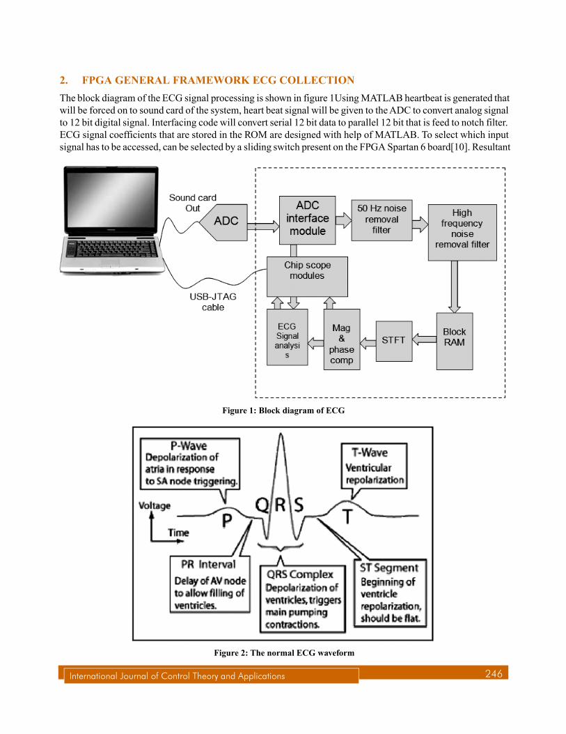
The block diagram of the ECG signal processing is shown in figure 1Using MATLAB heartbeat is generated that
will be forced on to sound card of the system, heart beat signal will be given to the ADC to convert analog signal
to 12 bit digital signal. Interfacing code will convert serial 12 bit data to parallel 12 bit that is feed to notch filter.
ECG signal coefficients that are stored in the ROM are designed with help of MATLAB. To select which input
signal has to be accessed, can be selected by a sliding switch present on the FPGA Spartan 6 board[10]. Resultant
Figure 1: Block diagram of ECG
Figure 2: The normal ECG waveform
A FPGA Based High Performance Heart Beat Monitoring System
signal is fed to Notch Filter. Notch filter is designed to operate at a frequency of 50 Hz (attenuation), in order to
remove power supply interference noise. Data thus obtained from the Notch filter is sent to high frequency noise
removal filter. This filter is designed to attenuate signals which are not in the range of 0.05 to 100Hz (allows
these frequencies only). The output from high frequency noise removal filter is given to block ram which store
the data in it and forwards data to STFT (Short Time Fourier Transform) block to process FFT on the signal.
STFT is developed by Xilinx IP core so Block ram is also embedded in the core. So external block ram is not
required as shown in block diagram, STFT is used to analyze frequency response of the heartbeat. Magnitude
and phase comparator module will carry out time domain analysis i.e. magnitude and time period of each wave
(P, Q, R, S & T) shown in figure 2[9] and the standard ECG values shown in table 1.
Table 1
standard ECG values
Amplitude Duration
P wave 0.25 mV P-R interval 0.12 to 0.20 Sec
R waveQ wave 1.60mV25% of R wave Q-T intervalS-T segment 0.35 to 0.44 Sec0.05 to 0.15 Sec
T wave 0.1 to 0.5mV P wave Interval 0.11 sec
QRS complex 0.09 Sec
PR segment 0.06 to 0.10 Sec
ST segmentT wave 0.10 to 0.15 secVaries
3. ADC MODULE
3.1. Analog input interface (ADC)
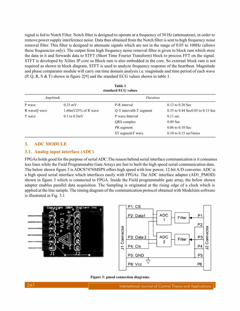
FPGAs holds good for the purpose of serial ADC.The reason behind serial interface communication is it consumes
less lines while the Field Programmable Gate Arrays are fast to built the high speed serial communication data.
The below shown figure 3 is ADCS7476MSPS offers high speed with low power, 12-bit A/D converter. ADC is
a high speed serial interface which interfaces easily with FPGAs. The ADC interface adapter (AD1_PMOD)
shown in figure 3 which is connected to FPGA. Inside the Field programmable gate array, the below shown
adapter enables parallel data acquisition. The Sampling is originated at the rising edge of a clock which is
applied at the line sample. The timing diagram of the communication protocol obtained with Modelsim software
is illustrated in Fig. 3.1
Figure 3: pmod connection diagrams.
B. Khaleelu Rehman, Adesh Kumar and Paawan Sharma
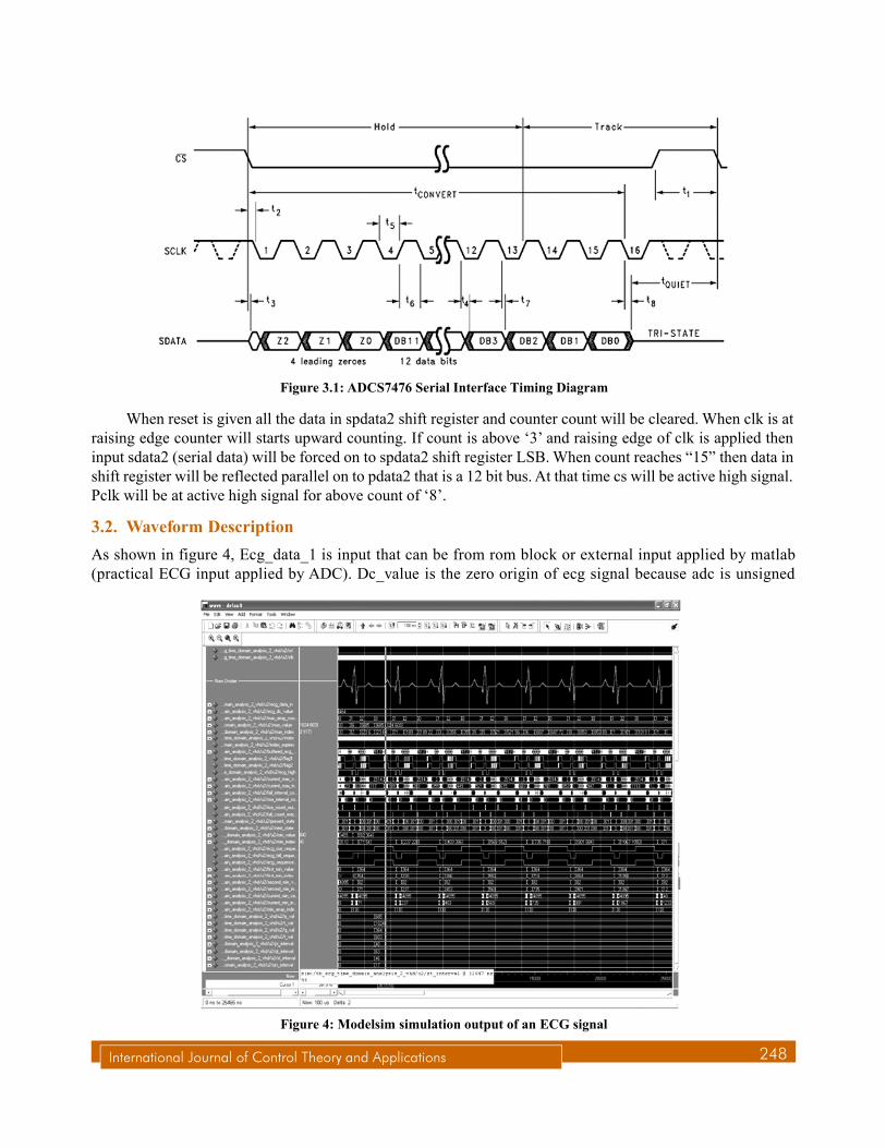
When reset is given all the data in spdata2 shift register and counter count will be cleared. When clk is at
raising edge counter will starts upward counting. If count is above ‘3’ and raising edge of clk is applied then
input sdata2 (serial data) will be forced on to spdata2 shift register LSB. When count reaches “15” then data in
shift register will be reflected parallel on to pdata2 that is a 12 bit bus. At that time cs will be active high signal.
Pclk will be at active high signal for above count of ‘8’.
3.2. Waveform Description
As shown in figure 4, Ecg_data_1 is input that can be from rom block or external input applied by matlab
(practical ECG input applied by ADC). Dc_value is the zero origin of ecg signal because adc is unsigned
Figure 3.1: ADCS7476 Serial Interface Timing Diagram
Figure 4: Modelsim simulation output of an ECG signal
A FPGA Based High Performance Heart Beat Monitoring System
hence cannot predict negative values. So +ve and –ve peaks are calculated by taking Dc_value as reference,
max_value and max_index are the peak values of P,R,T which are been generated add min_value and min_index
for Q and T.
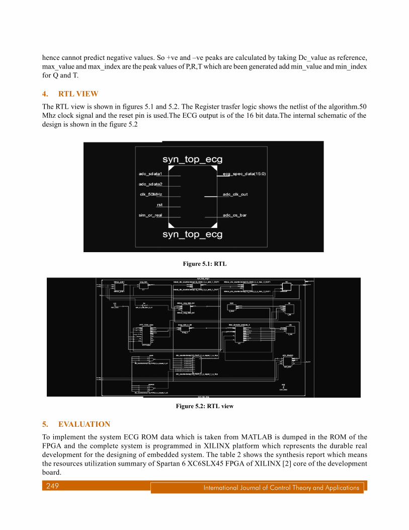
4. RTL VIEW
The RTL view is shown in figures 5.1 and 5.2. The Register trasfer logic shows the netlist of the algorithm.50
Mhz clock signal and the reset pin is used.The ECG output is of the 16 bit data.The internal schematic of the
design is shown in the figure 5.2
Figure 5.1: RTL
Figure 5.2: RTL view
5. EVALUATION
To implement the system ECG ROM data which is taken from MATLAB is dumped in the ROM of the
FPGA and the complete system is programmed in XILINX platform which represents the durable real
development for the designing of embedded system. The table 2 shows the synthesis report which means
the resources utilization summary of Spartan 6 XC6SLX45 FPGA of XILINX [2] core of the development
board.
B. Khaleelu Rehman, Adesh Kumar and Paawan Sharma
Table 2
Synthesis Report
ECFPGA2 Project Status (11/05/2016 - 15:22:03)
Project File: ECFPGA2.xise Parser Errors: No Errors
Module Name: syn_top_ecg Implementation State: Synthesized
Target Device: xc6slx45-3csg324 Errors: No Errors
Product Version: ISE 14.2 Warnings: No warnings
Design Goal: Balanced Routing Results: All Signals Completely Routed
Design Strategy: Xilinx Default (unlocked) Timing Constraints:
Environment: System Settings Final Timing Score: 0 (Timing Report)
Device Utilization Summary (estimated values) [-]
Logic Utilization Used Available Utilization
Number of Slice Registers 14 54576 0%
Number of Slice LUTs 43 27288 0%
Number of fully used LUT-FF pairs 14 43 32%
Number of bonded IOBs 7 218 3%
Number of BUFG/BUFGCTRLs 1 16 6%
6. SPARTAN 6 FPGA ECG FILTER DESIGN & CHIPSCOPE RESULTS
ChipScope is embedded software which is based on logic analyzer. By importing an “integrated controller core”
(icon) and an “integrated logic analyzer” (ila) into the design and making the connections properly, the design is
placed and routed using the implementation tools under XILINX ISE 14.2, and then download the bit stream file
into the target device to test and analysis the design which is carried out with the analyzer software.
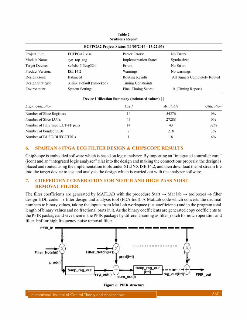
7. COEFFICIENT GENERATION FOR NOTCH AND HIGH PASS NOISE
REMOVAL FILTER.
The filter coefficients are generated by MATLAB with the procedure Start Mat lab toolboxes filter
design HDL coder filter design and analysis tool (FDA tool). A MatLab code which converts the decimal
numbers to binary values, taking the inputs from Mat Lab workspace (i.e. coefficients) and in the program total
length of binary values and no fractional parts in it. As the binary coefficients are generated copy coefficients to
the PFIR package and save them in the PFIR package by different naming as filter_notch for notch operation and
filter_bpf for high frequency noise removal filter.
Figure 6: PFIR structure
A FPGA Based High Performance Heart Beat Monitoring System
PFIR module: The package created which consist of the filter coefficients will be utilized by calling the
package in to program PFIR structure is shown in below figure 6. Input is taken as PFIR_in and is given to a
multiplier in a loop and another input to multiplier is the filter coefficient (i) stored in the PFIR package. Result
generated by the multiplier will be added with another multiplier in the loop (i+1). Loop will be running till last
coefficient is multiplied and result is reflected on to output signal PFIR_out
ECG Rom Block: An ECG signal is generated from MATLAB by using the command ECG for a sampling
rate of 160 the normal heartbeat rate is 72 beats per/min i.e. 0.83 sec for the beat so number of samples taken for
the beat is 160 samples . A MATLAB code has been developed to convert data in the workspace to binary format
according to specified length. The generated values in binary format is copied and saved in the ECG ROM. As
the clk is given the values are given to the output which will result in ECG signal
With the help of MATLAB and XILINX the ECG FIR filter design offers more effective channel. By using
XILINX IP core the FIR filter Can be easily designed through which low-pass filtering, high-pass filtering,
band-pass filtering and band-stop filtering can be achieved and the result of filtering is shown in figure 7. ECG
samples are stored the ROM unit of FPGA. First step is the removal of 50 Hz frequency interference through
FIR filter Then the second step is FIR high-frequency interference level filter scaling unit. In the storage unit of
ROM block ECG signals with frequency interference 150 Hz sinusoidal and 50Hz sinusoidal interference. The
first 50Hz frequency signal can be removed by using FIR distributed algorithms and hamming window for the
band-stop filter 45~55 Hz by taking the sampling frequency of 300 Hz. The second high-frequency interference
can be removed for FIR distributed algorithms, hamming window for the band-pass filter design 0.05~100 Hz
by taking the sampling frequency of 300 Hz. Earlier discussed first 50 Hz frequency interference of FIR filter
can decrease the power frequency noise of 40db whereas the second high frequency interference can decrease
the noise of 60db.
To verify results of the filtering the generated bit file is dumped in the target device Spartan-6 XC6SLX45.
Figure 7 shows the effect of filter with the help of chipscope pro analyzer software. From the figure 7, it can be
observed that the high-frequency interference and power frequency noise have a strong ability to filter. From the
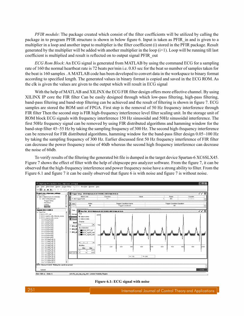
Figure 6.1 and figure 7 it can be easily observed that figure 6 is with noise and figure 7 is without noise.
Figure 6.1: ECG signal with noise
B. Khaleelu Rehman, Adesh Kumar and Paawan Sharma
8. CONCLUSION
The paper presents the Electrocardiogram signal FIR filtering design method implemented on Field Programmable
Gate Array board. The results discussed the effect of high-frequency noise interference and 50Hz power-frequency
interference noise with double filtering is observed. The filters may be directly used in the Field Programmable
Gate Array embedded ECG monitor design. This ECG monitor design system can be used to collect, store the
information, playback, wireless transmission and can be integrated into a FPGA chip, so as to reduce the utilization
of analog circuits, reducing development costs, and reducing the device utilization.
REFERENCES
[1] Yang Xue,, “Development of an ECG wireless monitoring system for home care based on GPRS”, Beijing university of
technology Lecture Notes in Electrical Enginnering, Springer, pp. 207-215, 2016.
[2] Lv Saojuan,Zhao Buhui. “Implemenattaion FIR digital filter,” Internation Journal of Microcomputer information”s, vol. 28,
pp. 1219-1227, 2015.
[3] Pan Jing ,Guo Xingming,Chne Min “Detection of ECG in remote in remote Electrocardiographic monitoring of computer
measurment & control ,” Vision, Image and Signal Processing, IEE Proceedings -, vol. 145, pp. 560-574, 2012.
[4] Aubert XL, “ Estimation of vital signs in bed from a single unobtusive mechanical sensor:Algoritms and real- life evaluation
“, In IEEE Engineering in medice and biology society conference proceedings, Spain, 2008.
[5] LIU Chang-sheng,TANG yan,XU wen-bin,DAI HUA, “Hardware system design of a wireless Electrocardiograph monitoring
terminal based on GPRS “, Microcomputer information, Volume 10,2010.
[6] Blanco-Velasco,M.Embeded filter bank-based algorithm for ECG compression ,” International Journal of signal processing”,
Volume 88(no 6) 2008.
[7] Wei jian-min,Yang young-ming,GUO Qiao-hui,”Design of real time ECG signals processing system based on FPGA”.,
International Journal of Electronic Devices 2015 vol(19) pno 142-156.
Figure 7: Filtered ECG signal.

A FPGA Based High Performance Heart Beat Monitoring System
[8] Suresh HN.Removal of EMG and ECG artifacts from EEG based on real time recurrent learning algorithm., International
Journal of physical sciences, 2008 Volume 3. No.5.
[9] N. Debbabi, S.El Asmi, H. Arfa, “Real-time Correction of ECG baseline wander Application to the Pan & Tompkins QRS
detection algorithm,” IEEE Transaction on signal Processing, vol. 10, pp. 1579-1592, Oct. 2014.
[10] XILINX internet site addredd(www.xilinx.com/support/documentation/user_guides/ug384.pdf)