Embed Size (px)
Citation preview

A HIGH-FREQUENCY QUAD-MODULUS PRESCALER
FOR FRACTIONAL-N FREQUENCY SYNTHESIZER
LAU WEE YEE WENDY
(B. Eng. (Hons.), NTU)
A THESIS SUBMITTED
FOR THE DEGREE OF MASTER OF ENGINEERING
DEPARTMENT OF ELECTRICAL & COMPUTER ENGINEERING
NATIONAL UNIVERSITY OF SINGAPORE
2009

i
ACKNOWLEDGEMENTS
Many people have played different roles in encouraging and inspiring me throughout
my course of graduate study at National University of Singapore (NUS). The
accomplishment of this thesis would not have been possible without the support and
guidance from all of them.
I would like to express my utmost gratitude and appreciation towards my supervisor,
Assistant Professor Yao Libin from Electrical & Computer Engineering (ECE)
Department of NUS, for his invaluable guidance and encouragements during my
course of study at NUS. This project would not have been completed without his
immense support, advice and guidance. I would also like to thank the ECE Department
for granting the commencement of this project. I am grateful towards the lecturers
from ECE Department for their remarkable teachings, and my course-mates for their
altruistic assistance.
I would like to express my heartfelt thanks to my former superiors, Mr. Fumio Muto
and Mr. Ivan Foo, from Cyrips Pte. Ltd. for supporting the project and providing a
conducive working environment which encourages research and development works. I
am grateful towards Dr. Zheng Jia Jun and Mr. Cheong Ban Chuan for sharing their
technical experiences, and providing advices and guidance. I wish to extend my
sincere thanks to my other colleagues, Ms. Qi Xiao Fei, Mr. Zhang Liang and Ms.
Chua Sue Suen, for their collaborations and understandings. All the skills and
experiences shared by my experienced colleagues will definitely be beneficial in my
future endeavours.

ii
I also wish to thank Associate Professor Siek Liter and Associate Professor Goh Wang
Ling from School of Electrical and Electronic Engineering of Nanyang Technological
University for encouraging me to further my study after my Bachelor’s Degree
graduation.
Last but not least, I would like to express my special thanks to my family members
and friends for their supports, encouragement and reassurance.

iii
TABLE OF CONTENTS
ACKNOWLEDGEMENTS......................................................................................... i
SUMMARY..... ........................................................................................................ vii
LIST OF FIGURES................................................................................................. viii
LIST OF TABLES .................................................................................................. xxi
CHAPTER 1 INTRODUCTION............................................................................... 1
1.1 Motivation........................................................................................... 1
1.2 Thesis Organization............................................................................. 2
CHAPTER 2 FREQUENCY SYNTHESIZER.......................................................... 4
2.1 Phase-Locked Loop (PLL)................................................................... 4
2.1.1 Frequency Multiplication ...................................................... 8
2.2 Frequency Synthesizer Architectures ................................................... 9
2.2.1 Direct Digital Frequency Synthesizer .................................... 9
2.2.2 Integer-N Frequency Synthesizer ........................................ 10
2.2.3 Fractional-N Frequency Synthesizer.................................... 13
2.2.4 Delay-Locked Loop (DLL) Frequency Synthesizer ............. 16
CHAPTER 3 PRESCALER....... ............................................................................. 17
3.1 Divide-by-2 Topologies..................................................................... 17
3.2 Synchronous and Asynchronous Dividers.......................................... 21
3.3 Dual-modulus Prescaler..................................................................... 22
3.4 Multi-modulus Prescaler.................................................................... 22
3.4.1 Ring Prescaler ..................................................................... 23
3.4.2 Phase-switching Prescaler ................................................... 23
CHAPTER 4 CIRCUIT DESIGN AND IMPLEMENTATION .............................. 26

iv
4.1 Fractional-N Frequency Synthesizer Circuit Overview, Architecture,
and Layout ................................................................................................. 26
4.1.1 Counters ............................................................................. 29
4.1.2 MASH ................................................................................ 34
4.1.3 Interface.............................................................................. 36
4.1.4 Mode Register..................................................................... 38
4.1.5 MUX_Output...................................................................... 40
4.1.6 PFD and Charge Pump........................................................ 40
4.1.7 Loop Filter and VCO .......................................................... 44
4.1.8 Fast-lock Control Switch..................................................... 49
4.1.9 Quad-modulus Prescaler ..................................................... 51
4.2 Quad-Modulus Prescaler Circuit Design............................................ 51
4.3 Frequency Synthesizer and Prescaler Layout ..................................... 61
4.4 Design Specifications ........................................................................ 62
4.5 PC Program for PLL Frequency Synthesizer Setting.......................... 65
4.5.1 User Interface ..................................................................... 65
4.5.2 Hardware Interface.............................................................. 67
CHAPTER 5 SIMULATION AND MEASUREMENT RESULTS ........................ 68
5.1 Testbenches....................................................................................... 68
5.1.1 Counters ............................................................................. 70
5.1.2 MASH ................................................................................ 78
5.1.3 Interface.............................................................................. 82
5.1.4 Mode Register..................................................................... 84
5.1.5 Fastlock .............................................................................. 86
5.1.6 Prescaler ............................................................................. 88

v
5.2 Simulation Results............................................................................. 89
5.2.1 Prescaler ............................................................................. 89
5.2.2 Frequency Synthesizer Current Consumption...................... 92
5.2.3 PLL Settings ....................................................................... 94
5.2.4 Prescaler Controller ............................................................ 95
5.2.5 N-Counter and MASH ........................................................ 96
5.2.6 Modulus Control............................................................... 100
5.2.7 PFD and Charge Pump...................................................... 101
5.2.8 Loop Filter ........................................................................ 104
5.3 Measurement Results....................................................................... 109
5.3.1 Test Plan........................................................................... 109
5.3.2 Operating Frequency Range .............................................. 110
5.3.4 Reference Spurs................................................................ 111
5.3.5 Fractional Spurs................................................................ 113
5.3.6 Integer-N Boundary Spur.................................................. 115
5.3.7 Loop Filter ........................................................................ 118
5.3.8 Phase Noise ...................................................................... 120
5.3.9 Crystal Oscillating Frequency ........................................... 120
5.3.10 Effect of Loop Bandwidth on Settling Time ...................... 121
5.3.11 Effect of Fastlock Function on Settling Time .................... 121
5.3.12 PC Program for PLL Setting (User Interface) .................... 122
CHAPTER 6 CONCLUSION............................................................................... 123
BIBLIOGRAPHY .................................................................................................. 129
APPENDICES.............................................................................................................136
Appendix A Reference Spur Plots............................................................136

vi
Appendix B Fractional Spur Plots............................................................139
Appendix C Integer-N Boundary Spurs...................................................150
Appendix D Phase Noise..........................................................................160

vii
SUMMARY
A fully integrated fractional-N frequency synthesizer which utilizes high-frequency,
fast-switching quad-modulus prescaler is proposed and demonstrated in this thesis. In
this proposed design, a quad-modulus prescaler with a divide-by-4/5/6 core is
implemented to minimize dynamic power consumption, avoid glitches and jitter due to
mismatch in input signals’ phases whilst maintaining high-frequency, fast-switching
capability. Besides, fast-lock function has been instigated in the synthesizer design to
reduce the frequency-locking time, and Multi-stAge noise SHaping (MASH)
technique has been utilized to reduce the overall phase noise and spurs. The proposed
frequency synthesizer offers technological robustness, fast locking capability,
versatility, low noise contribution, superior integration and deployment capacity, and
multi-modulus flexibility.
The proposed design has been studied, simulated at both circuit and system levels and
implemented to examine its performances. The actual circuit performances are verified
via measurements conducted after fabrication and packaging.
viii
LIST OF FIGURES
Figure 2.1: Role of frequency synthesizer in common transceiver............... 4
Figure 2.2: Phase-locked loop....................................................................... 5
Figure 2.3: Characteristic of phase detector.................................................. 6
Figure 2.4: Signals in a PLL.......................................................................... 6
Figure 2.5: Response of PLL to a small increase in frequency……………. 7
Figure 2.6: Linear approximation of PLL………………………………….. 8
Figure 2.7: Frequency multiplication of PLL…………………………….... 8
Figure 2.8: Direct digital frequency synthesizer with accumulator………... 9
Figure 2.9: An integer-N frequency synthesizer………………………….... 10
Figure 2.10: Frequency synthesizer with single modulus prescaler………… 11
Figure 2.11: High-frequency programmable divider……………………....... 12
Figure 2.12: Fractional-N synthesizer with: (a) pulse remover, (b) dual-
modulus prescaler………………………………........................
13
Figure 2.13: Noise shaping using ∆−∑ modulator……………………….... 14
Figure 2.14: First-order ∆−∑ modulator........................................................ 15
Figure 2.15: Delay-locked loop frequency synthesizer……………………... 16
Figure 3.1: Divide-by-2 circuit...................................................................... 18
Figure 3.2: Synchronous divider.................................................................... 21
Figure 3.3: Asynchronous divider................................................................. 21
Figure 3.4: Synchronous divide-by-4/5 circuit.............................................. 22
Figure 3.5: A cascaded divide-by-2/3 programmable prescaler.................... 23
Figure 3.6: A divide-by-2/3 core circuit........................................................ 24
Figure 3.7: A divide-by-2/3 using phase-switching....................................... 24

ix
Figure 4.1: Fractional-N frequency synthesizer block diagram.................... 28
Figure 4.2: R_Counter block diagram........................................................... 31
Figure 4.3: R_Counter_Bit schematic........................................................... 32
Figure 4.4: N_Counter block diagram........................................................... 33
Figure 4.5: Counter_Bit schematic................................................................ 34
Figure 4.6: MASH block diagram................................................................. 35
Figure 4.7: MASH_4order schematic............................................................ 35
Figure 4.8: Interface block diagram............................................................... 37
Figure 4.9: PLL synthesizer serial interface timing diagram......................... 38
Figure 4.10: Mode Register block diagram..................................................... 38
Figure 4.11: PFD state diagram....................................................................... 41
Figure 4.12: PFD block diagram...................................................................... 41
Figure 4.13: PFD_RSFF schematic................................................................. 42
Figure 4.14: CP block diagram........................................................................ 43
Figure 4.15: Linear model of PLL................................................................... 44
Figure 4.16: Schematic of third order loop filter............................................. 45
Figure 4.17: Schematic of loop filter with Fast-lock function......................... 48
Figure 4.18: LP_Filter schematic..................................................................... 49
Figure 4.19: Fastlock_Counter block diagram................................................ 50
Figure 4.20: State diagrams prescaler core...................................................... 52
Figure 4.21: Div16172021_top diagram.......................................................... 53
Figure 4.22: Input buffer schematic................................................................. 54
Figure 4.23: Effect of feedback resistor on buffer stability............................. 55
Figure 4.24: Div456_top block diagram.......................................................... 56
Figure 4.25: CML latch schematic.................................................................. 57

x
Figure 4.26: OR-embedded CML latch schematic.......................................... 59
Figure 4.27: OR gate schematic...................................................................... 60
Figure 4.28: Layout view of fractional-N frequency synthesizer.................... 61
Figure 4.29: Layout view of quad-modulus prescaler..................................... 62
Figure 4.30: Main user interface for synthesizer setting................................. 65
Figure 4.31: Second user interface for synthesizer setting.............................. 66
Figure 4.32: Third user interface displaying “Help” information................... 66
Figure 4.33: PLL setting through parallel port................................................ 67
Figure 5.1: PLL locking simulation testbench............................................... 68
Figure 5.2: Top level simulation testbench.................................................... 69
Figure 5.3: Testbench for AB_Counter functionality test............................. 70
Figure 5.4: Transient simulation results of AB_Counter............................... 71
Figure 5.5: Testbench for C_Counter functionality test................................ 72
Figure 5.6: Transient simulation results of C_Counter.................................. 73
Figure 5.7: Testbench for N_Counter functionality test................................ 74
Figure 5.8: Transient simulation results of N_Counter................................. 75
Figure 5.9: Testbench for R_Counter functionality test................................ 76
Figure 5.10: Transient simulation results of R_Counter.................................. 77
Figure 5.11: Testbench for 4th
order MASH functionality test........................ 78
Figure 5.12: Transient simulation result of MASH_4order............................. 79
Figure 5.13: Testbench for MASH top cell functionality test......................... 80
Figure 5.14: Transient response of MASH top cell......................................... 81
Figure 5.15: Testbench for Interface functionality test.................................... 82
Figure 5.16: Transient simulation results of Interface..................................... 83
Figure 5.17: Testbench for Mode Register functionality test.......................... 84

xi
Figure 5.18: Transient response of Mode_Reg................................................ 85
Figure 5.19: Testbench for Fastlock Counter functionality test...................... 86
Figure 5.20: Transient response of Fastlock_Counter..................................... 87
Figure 5.21: Testbench for div16172021_top functionality test...................... 88
Figure5.22: Minimum input signal amplitude requirement for prescaler....... 89
Figure 5.23: Current consumption of MASH in 45 cases................................ 93
Figure 5.24: Timing diagram of PLL setting................................................... 94
Figure 5.25: Dynamic characteristic of prescaler at Typical condition........... 95
Figure 5.26: Modulus-changing patterns in 2450MHz band........................... 96
Figure 5.27: Pulse interval of N-Counter output............................................. 97
Figure 5.28: Greatest common divisor of FN and FD..................................... 97
Figure 5.29: Error for pulse interval of N-Counter output.............................. 98
Figure 5.30: Noise shift characteristic of MASH............................................ 99
Figure 5.31: Noise level of PFD output at 6.25kHz ( REFf = 25MHz)............. 100
Figure 5.32: Delay of MOD_A in 45 cases..................................................... 100
Figure 5.33: Delay of MOD_B in 45cases...................................................... 101
Figure 5.34: Intercept of charge pump current in Typical condition............... 101
Figure 5.35: Intercept of charge pump current in 45 cases.............................. 102
Figure 5.36: Linearity of charge pump current with PFD at Typical
condition......................................................................................
103
Figure 5.37: Linearity of charge pump current with PFD at Typical condition......................................................................................
104
Figure 5.38: Locking curve of PLL without Fast-lock function at Typical
condition......................................................................................
105
Figure 5.39: Locking curve of PLL with Fast-lock function at Typical
condition......................................................................................
106
Figure 5.40: Synthesizer responses to frequency jumps.................................. 107

xii
Figure 5.41: Frequency ripple of synthesizer.................................................. 108
Figure 5.42: Timing diagram for PLL setting.................................................. 111
Figure 5.43: #5 frequency synthesizer reference spur plot at ~25MHz offset
(right)...........................................................................................
112
Figure 5.44: #5 frequency synthesizer reference spur plot at 10.80MHz
offset (left)...................................................................................
112
Figure 5.45: #5 frequency synthesizer reference spur plot at ~25MHz offset (left).............................................................................................
113
Figure 5.46: Fractional spurious levels at 2462.5MHz and 2463.3MHz......... 113
Figure 5.47: Integer-N boundary spurs for 2450.05MHz~2451.30MHz......... 115
Figure 5.48: Integer-N boundary spurs for 2451.35MHz~2451.85MHz......... 116
Figure 5.49: Integer-N boundary spurs at carrier frequency of 2451MHz
and offset of 1MHz with Moduli= 500, MASH=3, FN= 20.......
116
Figure 5.50: Integer-N boundary spurs at carrier frequency of 2451MHz
and offset of 1MHz with Moduli= 501, MASH= 3, FN= 20......
117
Figure 5.51: Effect of denominator on averaging the integer-N boundary
spurious levels.............................................................................
117
Figure 5.52: Effect of MASH order on integer-N boundary spurious levels.. 118
Figure 5.53: Frequency synthesizer’s phase noise performances.................... 120
Figure 5.54: User interface for PLL setting..................................................... 122
Figure A.1: #1 reference spur plot at ~25MHz offset (right)......................... 136
Figure A.2: #1 reference spur plot at 10.80MHz offset (left)......................... 136
Figure A.3: #1 reference spur plot at ~25MHz offset (left)............................ 136
Figure A.4: #2 reference spur plot at ~25MHz offset (right)......................... 136
Figure A.5: #2 reference spur plot at 10.80MHz offset (left)......................... 137
Figure A.6: #2 reference spur plot at ~25MHz offset (left)............................ 137
Figure A.7: #3 reference spur plot at ~25MHz offset (right)......................... 137
Figure A.8: #3 reference spur plot at 10.80MHz offset (left)......................... 137
xiii
Figure A.9: #3 reference spur plot at ~25MHz offset (left)............................
137
Figure A.10: #4 reference spur plot at ~25MHz offset (right)......................... 137
Figure A.11: #4 reference spur at 10.80MHz offset (left)................................ 138
Figure A.12: #4 reference spur at ~25MHz offset (left)................................... 138
Figure B.1: Fractional spur with carrier frequency of 2462.50MHz and offset at 25MHz...........................................................................
139
Figure B.2: Fractional spur with carrier frequency of 2462.50MHz and
offset at 50MHz...........................................................................
139
Figure B.3: Fractional spur with carrier frequency of 2462.50MHz and
offset at 75MHz...........................................................................
139
Figure B.4: Fractional spur with carrier frequency of 2462.55MHz and
offset at 25MHz...........................................................................
139
Figure B.5: Fractional spur with carrier frequency of 2462.55MHz and
offset at 50MHz...........................................................................
140
Figure B.6 Fractional spur with carrier frequency of 2462.55MHz and
offset at 75MHz...........................................................................
140
Figure B.7: Fractional spur with carrier frequency of 2462.60MHz and offset at 25MHz...........................................................................
140
Figure B.8: Fractional spur with carrier frequency of 2462.60MHz and
offset at 50MHz...........................................................................
140
Figure B.9: Fractional spur with carrier frequency of 2462.60MHz and offset at 75MHz...........................................................................
140
Figure B.10: Fractional spur with carrier frequency of 2462.65MHz and
offset at 25MHz...........................................................................
140
Figure B.11: Fractional spur with carrier frequency of 2462.65MHz and
offset at 50MHz...........................................................................
141
Figure B.12: Fractional spur with carrier frequency of 2462.65MHz and
offset at 75MHz...........................................................................
141
Figure B.13: Fractional spur with carrier frequency of 2462.70MHz and
offset at 25MHz...........................................................................
141
Figure B.14: Fractional spur with carrier frequency of 2462.70MHz and
offset at 50MHz...........................................................................
141

xiv
Figure B.15: Fractional spur with carrier frequency of 2462.70MHz and
offset at 75MHz...........................................................................
141
Figure B.16: Fractional spur with carrier frequency of 2462.70MHz and
offset at 100MHz.........................................................................
141
Figure B.17: Fractional spur with carrier frequency of 2462.75MHz and offset at 25MHz...........................................................................
142
Figure B.18: Fractional spur with carrier frequency of 2462.75MHz and
offset at 50MHz...........................................................................
142
Figure B.19: Fractional spur with carrier frequency of 2462.75MHz and offset at 75MHz...........................................................................
142
Figure B.20: Fractional spur with carrier frequency of 2462.75MHz and
offset at 100MHz.........................................................................
142
Figure B.21: Fractional spur with carrier frequency of 2462.80MHz and
offset at 25MHz...........................................................................
142
Figure B.22: Fractional spur with carrier frequency of 2462.80MHz and
offset at 50MHz...........................................................................
142
Figure B.23: Fractional spur with carrier frequency of 2462.80MHz and
offset at 75MHz...........................................................................
143
Figure B.24: Fractional spur with carrier frequency of 2462.80MHz and
offset at 100MHz.........................................................................
143
Figure B.25: Fractional spur with carrier frequency of 2462.85MHz and offset at 25MHz...........................................................................
143
Figure B.26: Fractional spur with carrier frequency of 2462.85MHz and
offset at 50MHz...........................................................................
143
Figure B.27: Fractional spur with carrier frequency of 2462.85MHz and
offset at 75MHz...........................................................................
143
Figure B.28: Fractional spur with carrier frequency of 2462.85MHz and
offset at 100MHz.........................................................................
143
Figure B.29: Fractional spur with carrier frequency of 2462.90MHz and
offset at 25MHz...........................................................................
144
Figure B.30: Fractional spur with carrier frequency of 2462.90MHz and
offset at 50MHz...........................................................................
144

xv
Figure B.31: Fractional spur with carrier frequency of 2462.90MHz and
offset at 75MHz...........................................................................
144
Figure B.32: Fractional spur with carrier frequency of 2462.90MHz and
offset at 100MHz.........................................................................
144
Figure B.33: Fractional spur with carrier frequency of 2462.95MHz and offset at 25MHz...........................................................................
144
Figure B.34: Fractional spur with carrier frequency of 2462.95MHz and
offset at 50MHz...........................................................................
144
Figure B.35: Fractional spur with carrier frequency of 2462.95MHz and offset at 75MHz...........................................................................
145
Figure B.36: Fractional spur with carrier frequency of 2462.95MHz and
offset at 100MHz.........................................................................
145
Figure B.37: Fractional spur with carrier frequency of 2463.00MHz and
offset at 25MHz...........................................................................
145
Figure B.38: Fractional spur with carrier frequency of 2463.00MHz and
offset at 50MHz...........................................................................
145
Figure B.39: Fractional spur with carrier frequency of 2463.00MHz and
offset at 75MHz...........................................................................
145
Figure B.40: Fractional spur with carrier frequency of 2463.00MHz and
offset at 100MHz.........................................................................
145
Figure B.41: Fractional spur with carrier frequency of 2463.05MHz and offset at 25MHz...........................................................................
146
Figure B.42: Fractional spur with carrier frequency of 2463.05MHz and
offset at 50MHz...........................................................................
146
Figure B.43: Fractional spur with carrier frequency of 2463.05MHz and
offset at 75MHz...........................................................................
146
Figure B.44: Fractional spur with carrier frequency of 2463.05MHz and
offset at 100MHz.........................................................................
146
Figure B.45: Fractional spur with carrier frequency of 2463.10MHz and
offset at 25MHz...........................................................................
146
Figure B.46: Fractional spur with carrier frequency of 2463.10MHz and
offset at 50MHz...........................................................................
146

xvi
Figure B.47: Fractional spur with carrier frequency of 2463.10MHz and
offset at 75MHz...........................................................................
147
Figure B.48: Fractional spur with carrier frequency of 2463.10MHz and
offset at 100MHz.........................................................................
147
Figure B.49: Fractional spur with carrier frequency of 2463.15MHz and offset at 25MHz...........................................................................
147
Figure B.50: Fractional spur with carrier frequency of 2463.15MHz and
offset at 50MHz...........................................................................
147
Figure B.51: Fractional spur with carrier frequency of 2463.15MHz and offset at 75MHz...........................................................................
147
Figure B.52: Fractional spur with carrier frequency of 2463.15MHz and
offset at 100MHz.........................................................................
147
Figure B.53: Fractional spur with carrier frequency of 2463.20MHz and
offset at 25MHz...........................................................................
148
Figure B.54: Fractional spur with carrier frequency of 2463.20MHz and
offset at 50MHz...........................................................................
148
Figure B.55: Fractional spur with carrier frequency of 2463.20MHz and
offset at 75MHz...........................................................................
148
Figure B.56: Fractional spur with carrier frequency of 2463.20MHz and
offset at 100MHz.........................................................................
148
Figure B.57: Fractional spur with carrier frequency of 2463.25MHz and offset at 25MHz...........................................................................
148
Figure B.58: Fractional spur with carrier frequency of 2463.25MHz and
offset at 50MHz...........................................................................
148
Figure B.59: Fractional spur with carrier frequency of 2463.25MHz and
offset at 75MHz...........................................................................
149
Figure B.60: Fractional spur with carrier frequency of 2463.25MHz and
offset at 100MHz.........................................................................
149
Figure B.61: Fractional spur with carrier frequency of 2463.30MHz and
offset at 25MHz...........................................................................
149
Figure B.62: Fractional spur with carrier frequency of 2463.30MHz and
offset at 50MHz...........................................................................
149

xvii
Figure B.63: Fractional spur with carrier frequency of 2463.30MHz and
offset at 75MHz...........................................................................
149
Figure B.64: Fractional spur with carrier frequency of 2463.30MHz and
offset at 100MHz.........................................................................
149
Figure C.1: Integer-N boundary spur with carrier frequency of 2450.00MHz................................................................................
151
Figure C.2: Integer-N boundary spur with carrier frequency of
2450.05MHz and offset at 50kHz...............................................
151
Figure C.3: Integer-N boundary spur with carrier frequency of 2450.10MHz and offset at 100kHz.............................................
152
Figure C.4: Integer-N boundary spur with carrier frequency of
2450.15MHz and offset at 150kHz.............................................
152
Figure C.5: Integer-N boundary spur with carrier frequency of
2450.20MHz and offset at 200kHz.............................................
152
Figure C.6: Integer-N boundary spur with carrier frequency of
2450.25MHz and offset at 250kHz.............................................
152
Figure C.7: Integer-N boundary spur with carrier frequency of
2450.30MHz and offset at 300kHz.............................................
152
Figure C.8: Integer-N boundary spur with carrier frequency of
2450.35MHz and offset at 350kHz.............................................
152
Figure C.9: Integer-N boundary spur with carrier frequency of 2450.40MHz and offset at 400kHz.............................................
153
Figure C.10: Integer-N boundary spur with carrier frequency of
2450.45MHz and offset at 450kHz.............................................
153
Figure C.11: Integer-N boundary spur with carrier frequency of
2450.50MHz and offset at 500kHz.............................................
153
Figure C.12: Integer-N boundary spur with carrier frequency of
2450.55MHz and offset at 550kHz.............................................
153
Figure C.13: Integer-N boundary spur with carrier frequency of
2450.60MHz and offset at 600kHz.............................................
153
Figure C.14: Integer-N boundary spur with carrier frequency of
2450.65MHz and offset at 650kHz.............................................
153

xviii
Figure C.15: Integer-N boundary spur with carrier frequency of
2450.70MHz and offset at 700kHz.............................................
154
Figure C.16: Integer-N boundary spur with carrier frequency of
2450.75MHz and offset at 750kHz.............................................
154
Figure C.17: Integer-N boundary spur with carrier frequency of 2450.80MHz and offset at 800kHz.............................................
154
Figure C.18: Integer-N boundary spur with carrier frequency of
2450.85MHz and offset at 850kHz.............................................
154
Figure C.19: Integer-N boundary spur with carrier frequency of 2450.90MHz and offset at 900kHz.............................................
154
Figure C.20: Integer-N boundary spur with carrier frequency of
2450.95MHz and offset at 950kHz.............................................
154
Figure C.21: Integer-N boundary spur with carrier frequency of
2451.00MHz and offset at 1.00MHz...........................................
155
Figure C.22: Integer-N boundary spur with carrier frequency of
2451.05MHz and offset at 1.05MHz...........................................
155
Figure C.23: Integer-N boundary spur with carrier frequency of
2451.10MHz and offset at 1.10MHz...........................................
155
Figure C.24: Integer-N boundary spur with carrier frequency of
2451.15MHz and offset at 1.15MHz...........................................
155
Figure C.25: Integer-N boundary spur with carrier frequency of 2451.20MHz and offset at 1.20MHz...........................................
155
Figure C.26: Integer-N boundary spur with carrier frequency of
2451.25MHz and offset at 1.25MHz...........................................
155
Figure C.27: Integer-N boundary spur with carrier frequency of
2451.30MHz and offset at 1.30MHz...........................................
156
Figure C.28: Integer-N boundary spur with carrier frequency of
2451.35MHz and offset at 1.35MHz...........................................
156
Figure C.29: Integer-N boundary spur with carrier frequency of
2451.40MHz and offset at 1.40MHz...........................................
156
Figure C.30: Integer-N boundary spur with carrier frequency of
2451.45MHz and offset at 1.45MHz...........................................
156

xix
Figure C.31: Integer-N boundary spur with carrier frequency of
2451.50MHz and offset at 1.50MHz...........................................
156
Figure C.32: Integer-N boundary spur with carrier frequency of
2451.55MHz and offset at 1.55MHz...........................................
156
Figure C.33: Integer-N boundary spur with carrier frequency of 2451.60MHz and offset at 1.60MHz...........................................
157
Figure C.34: Integer-N boundary spur with carrier frequency of
2451.65MHz and offset at 1.65MHz...........................................
157
Figure C.35: Integer-N boundary spur with carrier frequency of 2451.70MHz and offset at 1.70MHz...........................................
157
Figure C.36: Integer-N boundary spur with carrier frequency of
2451.75MHz and offset at 1.75MHz...........................................
157
Figure C.37: Integer-N boundary spur with carrier frequency of
2451.80MHz and offset at 1.80MHz...........................................
157
Figure C.38: Integer-N boundary spur with carrier frequency of
2451.85MHz and offset at 1.85MHz...........................................
157
Figure D.1: #1 (LF 1kHz) phase noise performance at 2450MHz at
10kHz offset................................................................................
160
Figure D.2: #1 (LF 1kHz) phase noise performance at 2450MHz at
20kHz offset................................................................................
160
Figure D.3: #1 (LF 1kHz) phase noise performance at 2450MHz at 50kHz offset................................................................................
160
Figure D.4: #1 (LF 1kHz) phase noise performance at 2450MHz at
200kHz offset..............................................................................
160
Figure D.5: #2 (LF 50kHz) phase noise performance at 2450MHz at
10kHz offset................................................................................
160
Figure D.6: #2 (LF 50kHz) phase noise performance at 2450MHz at
20kHz offset................................................................................
160
Figure D.7: #2 (LF 50kHz) phase noise performance at 2450MHz at
50kHz offset................................................................................
161
Figure D.8: #2 (LF 50kHz) phase noise performance at 2450MHz at
200kHz offset..............................................................................
161

xx
Figure D.9: #3 (LF 100kHz) phase noise performance at 2450MHz at
10kHz offset................................................................................
161
Figure D.10: #3 (LF 100kHz) phase noise performance at 2450MHz at
20kHz offset................................................................................
161
Figure D.11: #3 (LF 100kHz) phase noise performance at 2450MHz at 50kHz offset................................................................................
161
Figure D.12: #3 (LF 100kHz) phase noise performance at 2450MHz at
200kHz offset..............................................................................
161
Figure D.13: #4 (LF 200kHz) phase noise performance at 2450MHz at 10kHz offset................................................................................
162
Figure D.14: #4 (LF 200kHz) phase noise performance at 2450MHz at
20kHz offset................................................................................
162
Figure D.15: #4 (LF 200kHz) phase noise performance at 2450MHz at
50kHz offset................................................................................
162
Figure D.16: #4 (LF 200kHz) phase noise performance at 2450MHz at
200kHz offset..............................................................................
162
Figure D.17: #5 (LF 20kHz) phase noise performance at 2450MHz at
10kHz offset................................................................................
162
Figure D.18: #5 (LF 20kHz) phase noise performance at 2450MHz at
20kHz offset................................................................................
162
Figure D.19: #5 (LF 20kHz) phase noise performance at 2450MHz at 50kHz offset................................................................................
163
Figure D.20: #5 (LF 20kHz) phase noise performance at 2450MHz at
200kHz offset..............................................................................
163

xxi
LIST OF TABLES
Table 3.1: Latch topologies............................................................................. 18
Table 4.1: Proposed design specification for frequency synthesizer.............. 29
Table 4.2: PLL frequency synthesizer and operational mode register map.... 30
Table 4.3: Setting for order of MASH............................................................ 39
Table 4.4: Settings for output signal at “Counter_Out” pin............................ 39
Table 4.5: Charge Pump current control table................................................ 40
Table 4.6: Decoder control table..................................................................... 44
Table 4.7: Effect of prescaler moduli on minimum continuous divide ratio.. 51
Table 4.8: Moduli-control pins setting............................................................ 53
Table 4.9: Control logic for divide-by-4/5/6................................................... 56
Table 4.10: Power supply specification for PLL.............................................. 63
Table 4.11: Parameters of PLL counters, timer and registers........................... 63
Table 4.12: Theoretical frequency range of frequency synthesizer.................. 64
Table 4.13: Specifications for timing diagram of frequency synthesizer
settings...........................................................................................
64
Table 5.1: Operating ranges of prescaler in 45 cases...................................... 90
Table 5.2: Current consumptions of synthesizer building blocks at Typical
conditions (TT, 3.3V, 250C, 2450.05MHz)...................................
92
Table 5.3: Average current consumptions of synthesizer building blocks
in 45 cases......................................................................................
93
Table 5.4: Typical values of counters, registers and timer (crystal
oscillator frequency= 25MHz).......................................................
94
Table 5.5: Period of pseudo-random series..................................................... 98
Table 5.6: Pulse interval error of N-Counter output at various frequencies
and MASH order (FD= 500).........................................................
98
Table 5.7: Test conditions for frequency synthesizer.................................... 109

xxii
Table 5.8: Measurement equipments list........................................................ 109
Table 5.9: Simulation and measured operating frequency ranges.................. 110
Table 5.10: Frequency synthesizer reference spurs.......................................... 112
Table 5.11: Frequency synthesizer (Sample #5) fractional spurs..................... 114
Table 5.12: Loop filter designs......................................................................... 118
Table 5.13: Crystal oscillating frequency......................................................... 120
Table 5.14: Effect of loop bandwidth on settling time..................................... 121
Table 5.15: Effect of fastlock function on settling time................................... 122
Table 6.1: Summary table for fractional-N frequency synthesizer
performance...................................................................................
125
Table 6.2: Performance comparison with a few reported frequency
synthesizers....................................................................................
126
Table C.1: Integer-N boundary spurious levels at 2450MHz.......................... 150
Table C.2: Integer-N boundary spurious levels at carrier frequency of
2451MHz.......................................................................................
158

1
CHAPTER 1
INTRODUCTION
1.1 Motivation
The wireless communication market has been expanding, resulting in increasingly
stringent requirements for low cost, low power consumption, higher operating
frequencies and miniaturization on circuits due to limited battery life and highly
competitive market environment. Gallium Arsenide (GaAs) technology was used in
the early 80’s for implementation of circuits operating in the GHz bands. However,
silicon wafers is still preferred for its lower manufacturing cost, and improved unity-
gain bandwidth over the years via device scaling, new materials for interconnection,
and additional metal layers. Recent publications have highlighted the increasing
importance of CMOS RF circuits due to its compatibility with CMOS digital building
block, enabling the implementation of full RF System-on-Chip (SoC) [1].
Frequency synthesizer is one of the critical building blocks in integrated transceivers.
Conventional RF synthesizers are mostly integer-N synthesizers with output
frequencies fixed at integer multiples of reference frequency. Fractional-N synthesizer
is introduced because it allows deployment of higher reference frequency, contributing
to higher loop bandwidth, better phase noise suppression, faster loop settling time and
frequency flexibility. The only two blocks operating at full frequency in a synthesizer
are the voltage-controlled oscillator (VCO) and prescaler. In current CMOS
technology, it is easy to design high-frequency VCO but the prescaler remains as a
2
major challenge in high-frequency synthesizer design [2]. High-speed multi-modulus
prescaler are more intricate to be constructed as compared to fixed-division-ratio
divider and dual-modulus prescaler because the additional logic gates might slow
down the system.
Recent publications have demonstrated an increasing trend of proposing phase-
switching prescaler to rectify the lower operating speed inherited by conventional
synchronous divider [2, 3, 4]. However, phase-switching technique has glitches and
jitters due to phases mismatch issues which have to be addressed during
implementation. Besides, the need for Multiplexer and switching control blocks
increases the complexity of the circuit.
1.2 Thesis Organization
In Chapter 2, the principles of frequency synthesizer and the functionality of PLL are
discussed. Various frequency synthesizer architectures, together with their pros and
cons, are examined.
In Chapter 3, the fundamentals of prescaler are reviewed. Various divide-by-2
topologies, and their advantages and disadvantages are discussed. Besides, the
differences between synchronous and asynchronous dividers, dual-modulus and multi-
modulus prescalers are highlighted.

3
In Chapter 4, the circuit overview and implementations of the proposed frequency
synthesizer are presented, which includes counters, fast-lock timer, interface, mode
register, PFD, charge pump, quad-modulus prescaler, loop filter, etc..
In Chapter 5, the testbench setups, simulation results and measurement results of the
proposed design are presented.
In Chapter 6, a summary of the research has been outlined.

4
CHAPTER 2
FREQUENCY SYNTHESIZER
The output frequency of oscillator in an RF transceiver (transmitter-receiver) has to
meet the stringent requirements of high precision and capability of varying in small,
accurate steps. Hence, it is usually embedded in synthesizer which synthesizes clean,
fast-switching and programmable frequencies from one or more fixed reference
frequencies. Figure 2.1 shows the role of synthesizer in common transceiver
architecture.
Figure 2.1 Role of frequency synthesizer in common transceiver
2.1 Phase-Locked Loop (PLL)
PLL is a feedback system operating on the excess phase of nominally periodic signals.
Figure 2.2 shows a simple PLL comprising of phase detector (PD), low-pass filter
LNA
Duplexer
Filter
PA
Band Pass
Filter
Band Pass Filter
Frequency
Synthesizer
Channel
Selection

5
(LPF), and voltage-controlled oscillator (VCO). The loop is locked when the phase
difference, ∆Φ, is constant with time, resulting in equal input and output frequencies.
Figure 2.2 Phase-locked loop
PD acts as “error amplifier” in the feedback loop by minimizing ∆Φ between x(t) and
y(t). Under locked condition, it will produce an output with dc value that is
proportional to ∆Φ (Figure 2.3),
∆Φ∗= PDout Kv (2.1)
where KPD is the “gain” of the phase detector in V/rad. The LPF will pass the dc value
of the PD output while suppressing the high-frequency components. The dc value is
used to control the VCO such that it will oscillate at a frequency equals to the input
frequency but with a phase difference of ∆Φ [5]. Hence, VCO can be characterized by
outVCOFRout vK+= ωω and ( )
+∗= ∫
∞−
t
outVCOFRC dttvKtAty )(cos)( ω , with the input-
output transfer function given by
s
Ks
V
VCO
out
out =Φ
)( (2.2)
where ωFR is the “free-running” frequency and KVCO is the “gain” of VCO in rad/s/V.
Figure 2.4 shows an example of the signals at various points in a PLL with both input
and output signals having same frequency but finite phase difference.
y(t)
x(t) Phase
Detector
Low-pass
Filter
VCO

6
Figure 2.3 Characteristic of phase detector
Figure 2.4 Signals in a PLL
As shown in Figure 2.5, when a locked PLL experiences a small increase in frequency:
the input frequency, ωin, will be greater than the output frequency, ωout, temporarily;
x(t) will accumulate phase faster than y(t); PD will progressively generate wider
pulses. Wider pulse contributes to higher dc value at the LPF output, resulting in an
increase in VCO frequency. The increase in VCO frequency will reduce the difference
between ωin and ωout, resulting in the reduction of the width of PD output pulses and
the eventual settlement of dc value at a value which is slightly greater than its initial
locked-phase value [6]. Hence, the loop is locked only after both “frequency
acquisition” and “phase acquisition” are satisfied.
outV
Phase
Detector Vout
∆Φ
t
∆Φ

7
Figure 2.5 Response of PLL to a small increase in frequency
Although PLL has a nonlinear transient response, a linear approximation is used to
estimate its performance as shown in Figure 2.6. The closed-loop transfer function, or
jitter transfer function, is given by,
)(
)(
)(
)()(
sGKKs
sGKK
s
ssH
LPFVCOPD
LPFVCOPD
in
out
+=
Φ
Φ= (2.3)
If
LPF
LPF ssG
ω+
=
1
1)( and
RCLPF
1=ω ,
VCOPD
LPF
VCOPD
KKss
KKsH
++
=
ω
2)( (2.4)
22
2
2)(
nn
n
sssH
ωζω
ω
++= (2.5)
8
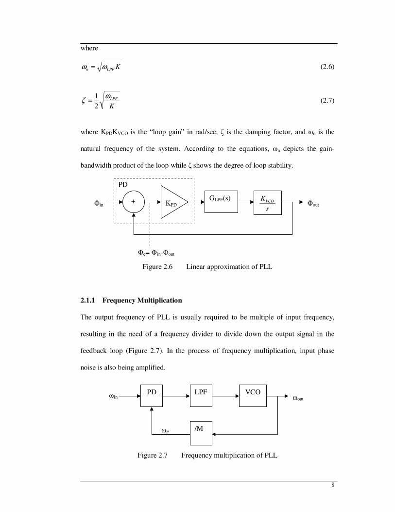
where
KLPFn ωω = (2.6)
K
LPFωζ
2
1= (2.7)
where KPDKVCO is the “loop gain” in rad/sec, ζ is the damping factor, and ωn is the
natural frequency of the system. According to the equations, ωn depicts the gain-
bandwidth product of the loop while ζ shows the degree of loop stability.
Figure 2.6 Linear approximation of PLL
2.1.1 Frequency Multiplication
The output frequency of PLL is usually required to be multiple of input frequency,
resulting in the need of a frequency divider to divide down the output signal in the
feedback loop (Figure 2.7). In the process of frequency multiplication, input phase
noise is also being amplified.
Figure 2.7 Frequency multiplication of PLL
PD LPF VCO
/M
ωin ωout
ωF
GLPF(s)
s
KVCO KPD + Φin Φout
Φe= Φin-Φout
PD
9
2.2 Frequency Synthesizer Architectures
The output frequencies, fout, of frequency synthesizers vary in steps of multiplications
of channel spacing: chout kfff += 0 , where f0 is the lower limit of frequency, k is the
number of channels and fch is the channel spacing. The use of PLL is often required
due to the requirement for high precision in the definition of f0 and fch. Some of the
frequency synthesizer architectures will be discussed in the following sections.
2.2.1 Direct Digital Frequency Synthesizer
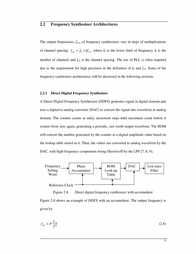
A Direct Digital Frequency Synthesizer (DDFS) generates signal in digital domain and
uses a digital-to-analog converter (DAC) to convert the signal into waveform in analog
domain. The counter counts in unity, increment steps until maximum count before it
restarts from zero again, generating a periodic, saw-tooth output waveform. The ROM
will convert the number generated by the counter to a digital amplitude value based on
the lookup table stored in it. Then, the values are converted to analog waveform by the
DAC, with high-frequency components being filtered-off by the LPF [7, 8, 9].
Figure 2.8 Direct digital frequency synthesizer with accumulator
Figure 2.8 shows an example of DDFS with an accumulator. The output frequency is
given by
M
CKout
fPf
2= (2.8)
Frequency
Setting Word
Phase
Accumulator
ROM
Look-up Table
DAC Low-pass
Filter
Reference Clock

10
where fCK is the clock frequency, P is the programmable step and M is the register bit
number.
DDFS has the following advantages: low phase noise due to avoidance of use of
analog VCO; fine frequency increments but at the expense of complexity; faster
channel switching capability as compared to PLL; continuous-phase channel switching;
direct modulation of output signal in digital domain. However, DDFS has the
following drawbacks: speed limitation due to highest-frequency limitation according
to Nyquist’s sampling theorem [5, 10, 11, 12]; spectral purity is limited by the speed,
resolution and power dissipation of DAC.
2.2.2 Integer-N Frequency Synthesizer
The integer-N frequency synthesizer is one of the most commonly used architecture.
As shown in Figure 2.9, the output frequency is given by chREFout kfffNf +=∗= 0 ,
where kNN L += ; k=0, 1,…, P. It shows that input reference frequency and channel
spacing must be the same.
Figure 2.9 An integer-N frequency synthesizer
A low fREF, which requires a narrow loop bandwidth to block the signal components at
fREF and its harmonics, is desired for small channel spacing. Settling time will increase
fREF PD LPF VCO fout
/M
Modulus select

11
and VCO noise suppression capability will decrease as a result of narrow loop
bandwidth. A divider with larger division value is needed for low fREF but this will
result in the increase of VCO in-band phase noise. Hence, this topology is not suitable
for systems which require low phase noise, fast switching time and small frequency
spacing [13].
A prescaler can be added when the VCO output frequency is higher than the
programmable divider maximum clock frequency, as shown in Figure 2.10. Under
locked condition, REFPout fNPf ∗∗= , where P is the programmable frequency divider
division ratio, NP is the prescaler division ratio, and REFP fN ∗ is the frequency
channel spacing. The drawbacks of this topology are larger frequency channel spacing,
smaller reference frequency, longer lock-on time, and sidebands.
Figure 2.10 Frequency synthesizer with single modulus prescaler
Dual-modulus prescaler is able to solve the frequency resolution problem by providing
two division ratios, i.e. NP and (NP+1), with the control signal from additional logic
circuit. Hence, a high-frequency programmable divider can be formed by combining a
dual-modulus prescaler with two counters, as shown in Figure 2.11.
PFD
LPF
VCO
Prescaler
/Np
Programmable
divider
/P
Reference frequency
fREF fout

12
Figure 2.11 High-frequency programmable divider
The prescaler will first divide by (NP+1) and the swallow counter will start counting
till it overflows at S. Then, the overflow bit will set the division ratio of prescaler to
NP while the program counter will start counting till it overflows at P. Both the S-
counter and P-counter will be reset and the division cycle repeats again. The overall
division is given by
( )[ ] ( )[ ] SPNSPNSNN PPP +=−++= 1 (2.9)
where P must be larger than S for proper reset operation by program counter, and
( )( ) )(01)( 2
minminmin PPPPP NNNNSNPN −=+−=+= (2.10)
maxmaxmax )( SNPN P += (2.11)
This topology has the following drawbacks: occurrence of reference spur; limited loop
bandwidth; higher close-in phase noise at the output.
Dual-modulus
prescaler
/Np, /(Np+1)
Programmable
counter
/P
Swallow counter
/S
modulus control
reset
fin fout
Channel selection

13
2.2.3 Fractional-N Frequency Synthesizer
As shown in Figure 2.12 is two fractional-N frequency synthesizer topologies. The
conventional design as shown in Figure 2.12(a) includes a pulse-remover which
removes one output pulse upon activation. The average output frequency is given by
prefout T
ff 1+= (2.12)
where Tp is the period when pulse-remove command is activated. Figure 2.12(b)
shows an alternative design using dual-modulus prescaler, with the phase accumulator
being clocked at reference frequency. Assuming a word of length Ldiv represents a
division-ratio setting at each clock cycle, the dual-modulus prescaler will divide by N
while the phase accumulator accumulates its output. Once the phase-accumulator-
output overflows, the prescaler will divide by (N+1). For an accumulator of length
Lacc, the accumulator will overflow Ldiv times per cycle. Hence, the average division
ratio is given by
( )
acc
div
acc
divdivaccave
L
LN
L
LNLLNN +=
++−=
1)( (2.13)
+=
acc
divrefout
L
LNff (2.14)
(a)
PDF LPF VCO
Pulse
remover
1/N
fREF fout

14
(b)
Figure 2.12 Fractional-N synthesizer with: (a) pulse remover, (b) dual-modulus
prescaler
The fractional-N frequency synthesizer allows for higher PLL loop bandwidths but the
main drawback is the appearance of fractional spurs. Under closed-loop condition,
with VCO output of REFfN )( α+ and periodic, ramp LPF output waveform of period
( )REFfα/1 , sidebands will appear at REFfα , REFfα2 , etc. with respect to centre
frequency. Fractional compensation can be implemented to suppress the fractional
spurs by injecting another current pulse series of similar width but opposite direction
to the low-pass filter. However, the major limitation is the inaccuracy due to
mismatches in the compensation current. Alternatively, ∆−∑ modulation method
(Figure 2.13) can be used to average out the division factor and convert the fractional
spurs to random noise before shaping the resultant noise spectrum and push it beyond
the loop bandwidth [13-18].
Figure 2.13 Noise shaping using ∆−∑ modulator
To PD
xF(t)
1/(N+1), 1/N
From VCO
fout
Σ∆
Modulator
b(t)
PFD LPF VCO fREF fout
overflow
/N, /(N+1)
Phase accumulator
Division-ratio
setting word

15
Figure 2.14 First-order ∆−∑ modulator
As shown in Figure 2.14 is a first-order ∆−∑ modulator. Input signal representing the
fractional value is input to the integrator before passing through the quantizer, which is
operating at higher sampling frequency with respect to the Nyquist frequency. The
transfer function of the integrator is given by
11
1)(
−−=
zzH (2.15)
The output of the first-order ∆−∑ modulator can be expressed as
)()(1
1)(
)(1
)()(
11zq
zHzzx
zHz
zHzy
++
+=
−− (2.16)
)()1()( 1zqzzx
−−+= (2.17)
)()()(1
zqzHzx noise
−+= (2.18)
where x(z) is the input signal and q(z) is the quantization noise. Hnoise, which is a high-
frequency component, can be filtered out by passing the signal via a low-pass filter.
A dithering enabled Σ-∆ modulator will further reduce the unwanted fractional spurs.
Dithering is a method of introducing random noise to the Σ-∆ modulator. One
technique involves one LSB dithering at the DC input but at the compromise of
x + 11
1−− z
1-bit
quantization
fs
z-1
y

16
synthesizer resolution because any changes in the DC input will directly affect the
output frequency. Another technique involves initializing the input word of first stage
accumulator to a value which is independent to the long term average of the Σ-∆
modulator [19].
2.2.4 Delay-Locked Loop (DLL) Frequency Synthesizer
Figure 2.15 shows a DLL frequency synthesizer with a voltage controlled delay line
in-place of the voltage controlled oscillator [20]. Under “locked” condition, the
difference between input and output of delay line is one reference clock cycle, TREF.
Hence, a synthesizer with N-delay stages will experience a delay of NTREF for each
stage. Each transition in the delay-line output will trigger a transition at the edge
combiner, causing the latter to produce an output frequency of REFNf .
Figure 2.15 Delay-locked loop frequency synthesizer
This topology has the following advantages: jitter will not be carried forward to
successive cycles; lower phase noise for adjacent frequencies; it does not require high
Q. However, it is not suitable for applications that entail frequency tuning because of
the fixed output frequency, which is determined by the number of delay stages.
Phase
Detector
Loop
Filter
Vctrl
fREF
Edge Combiner fout = NfREF
Voltage-controlled Delay Line
(with N delay elements)

17
CHAPTER 3
PRESCALER
Due to the inherent limitation to switching speed of CMOS digital cells [21], prescaler
is needed to divide down the VCO frequency before transmitting the signal to
programmable divider in high-frequency PLL-based synthesizer system [22]. Despite
the current advancement of CMOS process, the prescaler remains as a major challenge
in high-frequency design due to the trade-off between functionality and operating
speed [2, 3, 23, 24]. The various divider topologies and common implementations of
prescaler will be discussed in the following sections. Usually, the first few divider
blocks will utilize fast-switching, high-frequency divider topologies such as current
mode logic (CML) (also called source-coupled logic (SCL)) [25] and injection-locked
[26, 27]. Subsequent divider blocks, which operate at lower frequency, can utilize
simpler topologies such as True Single-Phase Clock (TSPC) to minimize overall
power consumption.
3.1 Divide-by-2 Topologies
Figure 3.1 shows a divide-by-2 structure (also called Johnson Counter) that is formed
using two cascaded latches. The maximum operating speed is determined by the
propagation delay of latches (delay1, delay2), i.e. the time taken for the input signal of
each latch to propagate to its respective output, and the setup time of latches (Ts)
sin Tdelay
T+⟩ 2,1
2 (3.1)
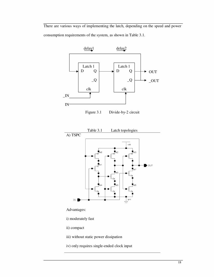
18
There are various ways of implementing the latch, depending on the speed and power
consumption requirements of the system, as shown in Table 3.1.
Figure 3.1 Divide-by-2 circuit
Table 3.1 Latch topologies
A) TSPC
Advantages:
i) moderately fast
ii) compact
iii) without static power dissipation
iv) only requires single-ended clock input
Latch 1
D Q
_Q
clk
Latch 1
D Q
_Q
clk
_IN
IN
delay1 delay2
OUT
_OUT

19
Drawbacks:
i) slower speed due to stacked PMOS
ii) signal passes through three gates per cycle
iii) requires full-swing input signal
B) Razavi’s [28]
Advantages:
i) fast due to absence of stacked PMOS
ii) signal passes through two gates per cycle
Drawbacks:
i) presence of static power dissipation
ii) requires full-swing, differential input signals
C) Wang’s [29]
Advantages:
i) fast due to absence of stacked PMOS
ii) signal passes through two gates per cycle
Drawbacks:
i) presence of static power dissipation
ii) requires full-swing, differential input signals

20
D) CML
Advantages:
i) very fast due to absence of PMOS
ii) signal passes through two gates per cycle
iii) requires smaller input swing
Drawbacks:
i) presence of static power dissipation
ii) requires differential input signals and biasing
iii) occupies larger chip area

21
3.2 Synchronous and Asynchronous Dividers
A synchronous divider uses a single clock signal to feed all the clock inputs
simultaneously, as shown in Figure 3.2. This approach introduces lower jitter but
higher power consumption due to high frequency operation of all registers, and higher
loading on the clock to drive all registers simultaneously. Figure 3.3 shows an
asynchronous divider with each divide-by-2 stage being clock by the output of the
preceding stage. Hence, this approach introduces lower power consumption with
subsequent stages consume lesser power while operating at lower frequency, and
lesser loading on the clock which only needs to drive the first stage but larger jitter.
Figure 3.2 Synchronous divider
Figure 3.3 Asynchronous divider
DFF1
D Q
_Q
clk _clk
DFF2
D Q
_Q
clk _clk
IN
_IN
_OUT
OUT
DFF1
D Q
_Q
clk _clk
DFF2
D Q
_Q
clk _clk
IN
_IN
OUT
_OUT

22
3.3 Dual-modulus Prescaler
A dual-modulus prescaler provides two division ratios, N and N+1, e.g. 16/17, 32/33,
64/65, 128/129, etc. [4]. Figure 3.4 shows a traditional synchronous divide-by-4/5
design. A modulus control signal, M, is used to control the division ratio to divide by
either N or N+1. As shown, when M=‘0’, D1 and D2 will form a divide-by-4 with q3
remaining at ‘High’ and NAND1 behaving like a NOT gate. When M=‘1’, NAND2 will
behave like a NOT gate and NAND1 will output ‘0’ when both q2 and q3 are at ‘High’.
Hence, q1 will change from high-to-low after 3 cycles of fclk, forming a divide-by-5.
Figure 3.4 Synchronous divide-by-4/5 circuit
3.4 Multi-modulus Prescaler
A multi-modulus prescaler provides multiple division ratios that are selected via
external control signals, which extend the functional frequency range of the system [2,
30].
NAND1
DFF1
D1 Q1
_Q1
clk _clk
DFF2
D2 Q2
_Q2
clk _clk
DFF3
D3 Q3
_Q3
clk _clk
NAND2
IN
_IN
M

23
3.4.1 Ring Prescaler
A series of divide-by-2/3 dividers can be cascaded to form a divider with division
ratios ranging from 2n to 2n+1-1 [31, 32]. Figure 3.5 shows a cascaded divide-by-2/3
design [33, 34]. The asynchronous topology allows the divider to function at a higher
speed with lower power consumption, but at the expense of accumulation of jitters.
Figure 3.5 A cascaded divide-by-2/3 programmable prescaler
3.4.2 Phase-switching Prescaler
Referring to Figure 3.6, the maximum operating speed of a divide-by-2/3 structure is
slower than basic divide-by-2 (Eqn. 3.1) due to the presence of gating logics
sin Tdelaydelay
T++⟩ 32,1
2 (3.2)
Hence, phase-switching topology is utilized to realize a divide-by-2/3 by multiplexing
the outputs of a divide-by-2 circuit (Figure 3.7). The maximum operating speed of this
structure is equivalent to the speed of a basic divide-by-2, with the multiplexer
operating at half of the input frequency. However, conventional phase-switching
prescaler that switches in “increasing cycle” (or anticlockwise) manner between output
phases may suffer from glitches [2, 3], and special attention is needed to ensure that
there is no mismatch in phases to avoid jitter.
3/2÷
3/2÷
3/2÷
CON0 CON1 CON2
IN OUT

24
Figure 3.6 A divide-by-2/3 core circuit
Figure 3.7 A divide-by-2/3 using phase-switching
Prescaler is required in high-frequency PLL system to overcome the issue of process
limitations. Higher modulus prescaler is desired to achieve larger N-value range,
especially the minimum N value [24]. The choice of prescaler architecture to be
implemented in a system will depend on the system’s requirements, such as power
consumption, phase noise, spurious level, etc..
Although phase-switching topology seems to be the most preferred architecture
recommended by literatures, it may face the issue of unwanted glitches during phase
DFF
D Q
_Q
clk _clk
MUX
Logic
_IN
IN
OUT
_OUT
CON
_OUT
Gating Logic
Latch 1
D Q
_Q
clk _clk
CON
_IN
IN
OUT
delay3 delay1 delay2
Latch 2
D Q
_Q
clk _clk

25
switching [23, 24]. Literatures have suggested various ways to remove the glitches [2-
4, 35]. A re-timer circuit is suggested by [35] to synchronize the input signals of
phase-switching control block at the expense of circuit complexity, power
consumption and die size. In [36], glitches are removed by reversing the switching
sequence but the switching control logic may not be sufficiently fast to detect the
switching from one phase to another. In [24], “time borrowing” technique is suggested
to overcome the switch-control-logic speed problem at the expense of power
consumption and additional pulse-generator block. In [2, 3], 8 output phases are used
to produce desired output signals and to reduce the error window but with increased
circuit complexity. Unfortunately, all these glitch-removing techniques either increase
circuit power consumption and/or reduce maximum operating frequency.
Other topologies possess respective shortcomings such as large power consumption,
lower maximum operating frequency, narrow locking range, large die size, etc. [2, 3,
26]. In [37], injection-locked technique is proposed for very high frequency operation
at the expense of very narrow operating range. In [38, 39], TSPC is used but this
topology has low input sensitivity due to the need for rail-to-rail input signal swing
and high switching noise. In [40], n divide-by-2/3 blocks are cascaded to form multi-
modulus prescaler. Although the cascaded structure provides option for power
optimization and reusability, special care is required in the design of divider because
reduction in time window between arrival of input feedback signal and successive
input clock edge will limit the maximum operating frequency.
Hence, high-speed, low-power and robust prescaler design remains as a challenge in
high-frequency synthesizer design.

26
CHAPTER 4
CIRCUIT DESIGN AND IMPLEMENTATION
As discussed in Chapter 2, fractional-N frequency synthesizer offers an improvement
on the phase noise by )log(20 F× , theoretically, while remaining competitive in terms
of current consumption, circuit complexity, and die size. The major concern with this
implementation is the spurious signal at VCO, caused by the phase perturbation during
divide-ratios switching. Delta-sigma modulation technique is a widely implemented
solution to address this problem. If the divide-ratio remains unchanged with increasing
switching frequency over F cycles, phase noise will be pushed to higher frequencies
before being filtered out by loop filter. Hence, the remaining noise will only exist at
low frequency, resulting in an overall improvement of phase noise performance.
Instead of direct phase-noise cancellation, this noise-shaping technique utilizes
switching-pattern modification to suppress the low frequency spectral caused by
divide-ratio switching.
4.1 Fractional-N Frequency Synthesizer Circuit Overview,
Architecture, and Layout
A high-frequency, fast-locking fractional-N PLL frequency synthesizer that utilizes
quad-modulus prescaler has been designed. In this design, fast-lock timer has been
incorporated to shorten the frequency locking time, Multi-stAge noise SHaping
(MASH) technique is implemented to reduce the phase noise and spurs, and quad-

27
modulus prescaler is employed to extend the system’s functional frequency range.
Hence, the proposed design offers technology robustness, versatility, fast locking
ability, low noise contribution, high integration competency, multi-modulus flexibility,
and ease of future expansion and deployment activities.
The design was realized using Chartered Semiconductor 0.35µm, 2P4M, CMOS
technology with MIM capacitor option. The system and circuit levels’ analyses,
designs and simulations were carried out in Cadence IC5.0.33 under Redhat 8.0 and
Cadence IC5.1.41 under Red Hat Enterprise Linux WS release 4 (Nahant Update 4).
All the basic digital cells are Synopsys standard cells.
Figure 4.1 shows the topology of the fractional-N frequency synthesizer design. The
design consists of the following building blocks: R-Counter, N-Counter, Fast-lock
Timer, MASH, Interface, Mode Register, MUX_Output, Phase-Frequency Detector
(PFD), Charge Pump, Fast-lock Control Switch, Quad-modulus Prescaler, and Loop
Filter. R-Counter will divide down the input reference frequency. Then, PFD will
compare this divided reference signal with the divided Local Oscillator (LO) signal
and generate two outputs which are not complementary. The PFD outputs are used to
drive charge pump that provides several gains to cater for the variation in VCO gain.
The variable charge pump gain ensures that the PLL loop gain is stable. Loop filter is
implemented with fast-lock function to shorten the locking time significantly.
Subsequently, the filtered signal is used to control the VCO frequency.
Then, the VCO differential output signals are divided by quad-modulus prescaler
before transmitting to N-Counter because digital circuit usually has lower functional

28
frequency. N-Counter, which supports 910MHz and 2450MHz operations, provides
whole-number division to the signal while the 3rd/4th order MASH produces fractional
output frequency. The divided signal is then compared with the divided reference
frequency. Hence, frequency locking is accomplished through these procedures. Table
4.1 lists the proposed design specification for the frequency synthesizer design.
Figure 4.1 Fractional-N frequency synthesizer block diagram
R-Counter PFD Charge
Pump
N-Counter
∆-Σ
Prescaler
Interface
Mode
Register
Fast-lock
Timer
PLL_DATA
PLL_CLK
PLL_LE
fREF_IN
VCO
Loop Filter
DATA
CLK
LE_NR
LE_FN
LE_FD
LE_MODE
RESET
5
DATA
CLK
LE_MODE
MASH_ORDER
CP0
CP1
CP2
FL_DATA
CP
2
CP
1
CP
0
FL_DATA
CLK

29
Table 4.1 Proposed design specification for frequency synthesizer
Parameter Unit Min Typ Max
Operating frequency MHz 2400.0 2450.0 2500.0
Operating voltage V 3.0 3.3 3.6
Current consumption mA <25.0
Operating temperature 0C -40.0 +85.0
Simulation temperature 0C -40.0 +27.0 +90.0
Reference frequency MHz 25.0
Channel spacing kHz 50.0
Modulus P 16/17/20/21
4.1.1 Counters
There are three counters, namely R-Counter, N-Counter and Fast-lock Timer. Both the
R-Counter and Fast-lock Timer have same counting units, which are implemented
using complete synchronous logic design for easy expansion to higher number of bits,
but different control units. There are hardware handshaking signals between the
counting unit and control unit, and there is no process-related delay cell involved so as
to ease the deployment of the counters to other process. N-counter consists of A-
Counter, B-Counter and C-Counter. It is capable of supporting 910MHz and 2450MHz
operations, with its initial value varying according to the output of MASH.
Table 4.2 shows the register map for the six registers in the frequency synthesizer,
namely: R-Counter Register, N-Counter Register, FN Register, FD Register, Fast-lock
Timer Register, and Operational Mode Register.

30
Table 4.2 PLL frequency synthesizer and operational mode register map
Counter/
Register
C0 C1 2 3 4 5 6 7 8 9 10 11 12 13/
18
14/
19
RN 0 0 R0 R1 R2 R3 N0 N1 N2 N3 N4 N5 N6 N7 N8
FN 1 0 FN0 FN1 FN2 FN3 FN4 FN5 FN6 FN7 FN8 X(Don’t Care)
FD 0 1 FD0 FD1 FD2 FD3 FD4 FD5 FD6 FD7 FD8 X(Don’t Care)
MODE 1 1 MO CO0 CO1 CP0 CP1 CP2 FLE FL0 FL2 FL3 ... FL10 FL11
The R-Counter Register has 4 bits, represented by R0 (least significant bit, LSB) to R3
(most significant bit, R3); N-Counter Register has 9 bits, represented by N0 (LSB) to
N8 (MSB); FN Register has 9 bits, represented by FN0 (LSB) to FN8 (MSB); FD
Register has 9 bits, represented by FD0 (LSB) to FD8 (MSB); Operational Mode
Register has 7 bits, represented by MO, CO0, CO1, CP0, CP1, CP2 and FLE.
R-Counter
R-Counter divides down the frequency of input reference signal, and PFD will
compare the divided reference signal to the divided LO signal. Assuming the R-
Counter input signal has frequency INREFf _ , R-Counter output signal has frequency
REFf , and R-Counter has value R,
R
ff
INREF
REF
_= (4.1)
If the built-in crystal PAD and external crystal are the reference source, INREFf _ is the
oscillating frequency of the crystal.

31
Figure 4.2 R_Counter block diagram
RE
SE
T f
un
ctio
n
Ou
tpu
t M
UX

32
Figure 4.3 R_Counter_Bit schematic
Figure 4.2 shows the block diagram of reference counter (i.e. R_Counter), which
consists of 4-bit shift register, 4-bit synchronous counter, comparator and reset
function when counter is full. Each bit counter (i.e. R_Counter_Bit) is implemented as
shown in Figure 4.3. After the data (i.e. R0-R3) from the register has been latched onto
R-Counter, bit-comparator will start comparing each data bit with the respective
counter’s output bit. The synchronous counter will start counting from “0000” until all
DATA_OUT=Bit_Out, and fREF_IN is being divided by R during the process and output
as fREF. Then, RESET function will send a “0” to all bit counters to clear the counter
back to “0000”. Once the reset is accomplished, signal will be fed back to the reset
logic. RESET will send a “1” to all bit counters and R-Counter is ready for the next
counting cycle.
N-Counter
Figure 4.4 shows the implementation of N-Counter, which is formed by A-Counter, B-
Counter and C-Counter. Assuming the minimum division ratio of prescaler is P and it
is a multiple of 4, the counters must satisfy the following conditions:
T Q
_Q
CDN
D Q
_Q
D Q
DATA_IN
CLK LE
DATA_OUT
A_Out
Bit_Out Bit_In
Bit_CLK
RESET
Bit_Comp
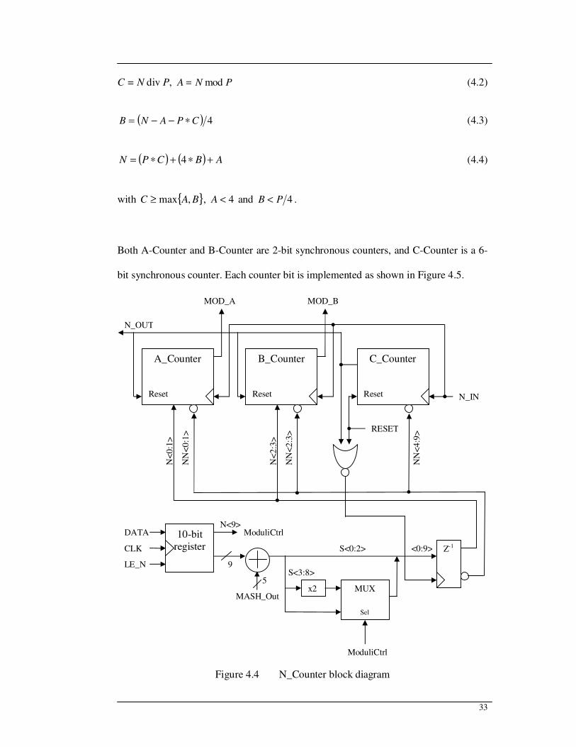
33
C = N div P, PNA mod= (4.2)
( ) 4CPANB ∗−−= (4.3)
( ) ( ) ABCPN +∗+∗= 4 (4.4)
with BAC ,max≥ , 4<A and 4PB < .
Both A-Counter and B-Counter are 2-bit synchronous counters, and C-Counter is a 6-
bit synchronous counter. Each counter bit is implemented as shown in Figure 4.5.
Figure 4.4 N_Counter block diagram
10-bit
register
DATA
CLK
LE_N
ModuliCtrl N<9>
MASH_Out MUX
Sel
x2
ModuliCtrl
Z-1
9
5
S<0:2>
S<3:8>
<0:9>
A_Counter
Reset
B_Counter
Reset
C_Counter
Reset N_IN
RESET
N_OUT
MOD_A MOD_B
N<
0:1
>
N<
2:3
>
NN
<0
:1>
NN
<2
:3>
NN
<4
:9>

34
Figure 4.5 Counter_Bit schematic
The pseudo-random number from MASH is added to the N-Counter register value, and
set as the initial value for N-Counter. N-Counter will divide down the Prescaler output
frequency before feeding the signal back to MASH and PFD, and generate the
Prescaler division-ratio control signals (MOD_A and MOD_B).
4.1.2 MASH
MASH generates pseudo-random numbers based on the numerator and denominator
value set by FN Register and FD Register respectively, and can function as a third-
order or forth-order modulator. The generated pseudo-random number is added to the
value indicated by N-Counter Register, and set as initial value of N-Counter. N-
Counter divides down the frequency of LO signal, and PFD will compare the divided
LO signal to the divided reference signal. Assuming LO signal has frequency LOf , and
prescaler has modulus value P ,
REFLO fFD
FNNPf ∗
+∗= (4.5)
where N is the value of N-Counter Register, FN is the value of FN Register, and FD is
the value of FD Register. Figure 4.6 shows the block diagram of MASH, and Figure
T Q
_Q
CDN
Bit_In
Bit_CLK
RESET
Bit_Out
Bit_Comp
NN

35
4.7 shows the implementation of four order MASH with option of choosing either 3rd
or 4th order via the “ORDER”pin.
Figure 4.6 MASH block diagram
Figure 4.7 MASH_4order schematic
D_Register
(2’s complement)
DATA F_Register
CLK
LE_F
LE_D
MASH 4order
ORDER
N_OUT
8
8
MASH_Out 5
RESET
F<0:8>
Z-1
Z-1
Z-1
Z-1
Accumulator
C1D1
C2D1
C2D2
C3D1
C3D2
C3D3
Z-1
D<0:8>
Z-1 Z-1
Z-1
Z-1
Z-1
C0
C1
C2
C3
C0
C1
C2
C3
ORDER
5 CA
A
B
A+B
A
B
A+B
A
B
A+B
A
B
A+B

36
After the DATA is latched to the outputs of F-register (denotes as FO) and D-register
(denotes as DO) respectively, at the rising edge of N_OUT pulse (i.e. the clock for
MASH_4order)
For 3,2,1,0=i ,
)()1()( ipSumipSumiSum +−= (4.6)
If DOiSum ≥)( ,
1=Ci ; DOiSumipSum −= )()( (4.7)
Else
0=Ci ; )()( iSumipSum = (4.8)
If 3=ORDER ,
( ) 22122211103 DCDCCDCCCMO +∗−+−+= (4.9)
If 4=ORDER ,
( ) ( ) 33233133334 DCDCDCCMOMO −∗+∗−+= (4.10)
where FOpSum =− )1( , MO3 = MASH_Out 3rd
order, MO4 = MASH_Out 4th
order.
4.1.3 Interface
The 3-wire serial interface is designed for receiving external PLL control commands,
enabling frequency setting and output signal selection. It abides by an industrial
standard timing diagram. Figure 4.8 illustrates the block diagram of Interface.

37
Figure 4.8 Interface block diagram
Data is latched into selective register(s) via the use control bits, i.e. C0 and C1, of the
Interface (Table 4.2). R-Counter Register and N-Counter Register share the same
control-bits configuration, while Operational Mode Register and Fast-lock Timer
Register share the same configuration. The serial data is clocked on the rising edge of
the serial clock, and is latched into the destined registers on the rising edge of PLL_LE,
as shown in Figure 4.9.

38
C0C1Bit2
PLL_LE
PLL_DATA
PLL_CLK
MSB
tdcs
tdch
tcwh
tcwl
tlw
tcls
tcr
tcf
tlf
tlr
*Symbol definitions are defined in Table 4.12
Figure 4.9 PLL synthesizer serial interface timing diagram
4.1.4 Mode Register
Mode Register is used to set the MASH order, output signal from frequency
synthesizer, and the charge pump current. Figure 4.10 shows the Mode Register block
diagram, which is formed by 6-bit serial-in, parallel-out shift register and 6-bit
parallel-in, parallel-out shift register.
Figure 4.10 Mode Register block diagram
6-bit parallel-in, parallel-out
shift register
LE_MODE
DATA
CLK
MASH_Order
Counter_Out_0
Counter_Out_1
CP0
CP1
CP2
6-bit serial-in, parallel-out
shift register DATA_OUT

39
Operating Mode Register has 7 bits, i.e. MO, CO0, CO1, CP0, CP1, CP2 and FLE
(Table 4.2). The order of MASH, i.e. 3rd order or 4th order, is set by MO as depicted by
Table 4.3.
Table 4.3 Setting for order of MASH
MO MASH order
0 3
1 4
CO0 and CO1 are used to select the output signal to be transmitted to “Counter_Out”
pin, from the output of R-Counter, Prescaler, Divider_N or Lock Detect. The settings
are as defined in Table 4.4.
Table 4.4 Settings for output signal at “Counter_Out” pin
CO0 CO1 Output at “Counter_Out”
0 0 R-Counter
1 0 Prescaler
0 1 Divider_N
1 1 Lock Detect
Fast-Lock Enable (FLE) bit is used to activate or de-activate the fast-lock function
with bit value “1” or “0”, respectively. FLE, CP0, CP1 and CP2 will set the Charge
Pump current, in accordance with Table 4.5.

40
Table 4.5 Charge Pump current control table
CP2 CP1 CP0 Current
(µA)
0 0 0 200
0 0 1 400
0 1 0 600
0 1 1 800
1 0 0 2000
1 0 1 3200
4.1.5 MUX_Output
MUX_Output is an output driver for the selection and transmission of output signals
from R-Counter, prescaler, divider and lock detector.
4.1.6 PFD and Charge Pump
PFD compares the phase and frequency difference between reference signal and
divided LO signal while Charge Pump will either source or sink current from the
external loop-filter. In this design, Charge Pump supports fast-lock function and has
six available current selections.
The operation of the PFD is as follow:
• if INDIVINREF ff __ > , positive pulses will be generated at UP while DN=0
• if INDIVINREF ff __ < , positive pulses will be generated at DN while UP=0
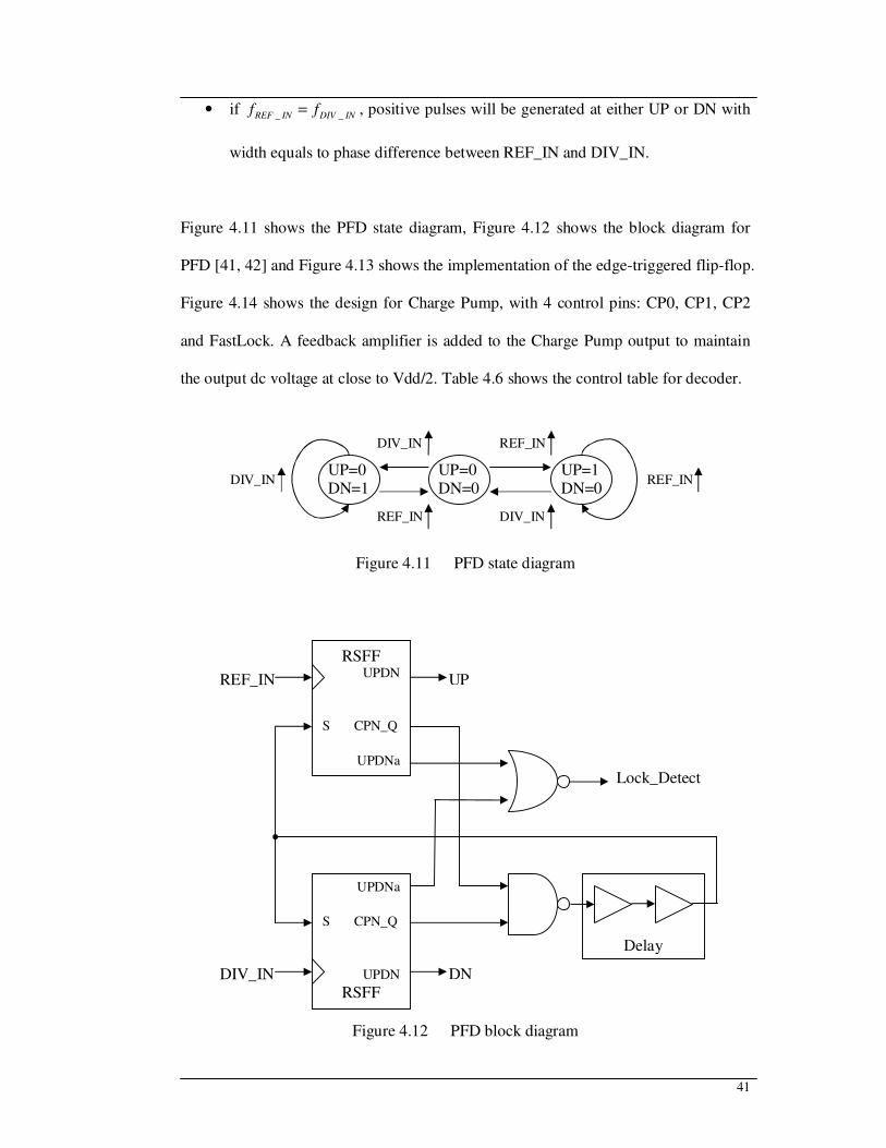
41
• if INDIVINREF ff __ = , positive pulses will be generated at either UP or DN with
width equals to phase difference between REF_IN and DIV_IN.
Figure 4.11 shows the PFD state diagram, Figure 4.12 shows the block diagram for
PFD [41, 42] and Figure 4.13 shows the implementation of the edge-triggered flip-flop.
Figure 4.14 shows the design for Charge Pump, with 4 control pins: CP0, CP1, CP2
and FastLock. A feedback amplifier is added to the Charge Pump output to maintain
the output dc voltage at close to Vdd/2. Table 4.6 shows the control table for decoder.
Figure 4.11 PFD state diagram
Figure 4.12 PFD block diagram
RSFF UPDN
S CPN_Q
UPDNa
UPDNa
S CPN_Q
UPDN
RSFF
REF_IN
DIV_IN DN
UP
Lock_Detect
Delay
UP=0 DN=1
UP=0 DN=0
UP=1 DN=0
DIV_IN
REF_IN DIV_IN
REF_IN
REF_IN DIV_IN

42
Figure 4.13 PFD_RSFF schematic
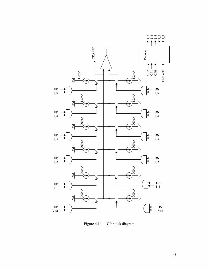
43
Figure 4.14 CP block diagram
UP
Vdd
20
0uA
20
0uA
Vd
d
20
0uA
20
0uA
Vd
d
20
0uA
20
0uA
Vdd
20
0uA
20
0uA
Vdd
DN
Vdd
UP
I_1
DN
I_1
DN
I_2
UP
I_2
DN
I_3
UP
I_3
1.2
mA
1.2
mA
Vdd
DN
I_4
UP
I_4
1.2
mA
1.2
mA
Vdd
DN
I_5
UP
I_5 C
P_
OU
T
Dec
oder
C
P2
CP
1
CP
0
Fast
Lock
I_5
I_4
I_3
I_2
I_1

44
Table 4.6 Decoder control table
Decoder output Fastlock CP2 CP1 CP0
I_5 I_4 I_3 I_2 I_1 I_0
CP_OUT
(µA)
0 0 0 0 0 0 0 0 0 1 200
0 0 0 1 0 0 0 0 1 1 400
0 0 1 0 0 0 0 1 1 1 600
0 0 1 1 0 0 1 1 1 1 800
0 1 0 0 0 1 1 1 1 1 2000
0 1 0 1 1 1 1 1 1 1 3200
0 1 1 0 0 0 1 1 1 1 800
0 1 1 1 0 0 1 1 1 1 800
1 x x x 1 1 1 1 1 1 3200
4.1.7 Loop Filter and VCO
Loop Filter is constructed by external resistors and capacitors, and modified according
to measurement results. VCO is represented by Verilog-A code for the functional test
of the synthesizer. In order to analyze the loop filter, the entire PLL loop has to be
taken into consideration. Figure 4.15 shows the linear model of PLL.
Kd
Z(s)θref θ
o
θN
s
KVCO
N
1
θeΣ
+
-
Figure 4.15 Linear model of PLL
The output current of PFD and Charge Pump is given by

45
( ) edd KtI θ= (4.11)
where θe is the phase error and Kd is the PFD gain. The VCO angular frequency ω is
( ) ( )fuKt fVCO+= 0ωω (4.12)
where KVCO is the VCO gain in rad.s
-1.V
-1. The open-loop gain of PLL is defined as
s
sZ
N
KKsG VCOd
e
N )()( ==
θ
θ (4.13)
where N is the division ratio of frequency divider and Z(s) is the loop filter transfer
function.
The fourth order PLL has a third order loop filter as demonstrated by the schematic in
Figure 4.16.
R1
C1 C3 C2
R2 VI
Figure 4.16 Schematic of third order loop filter
The transfer impedance of loop filter can be expressed as
+
+
+
+
+
=
++
==
3
2
2
1
1
2
2
2
3
2
1
22
1
1
1
1
1
1
1
1)(
sC
sCR
sCR
sCR
sCZ
Z
Z
ZsC
I
VsZ (4.14)
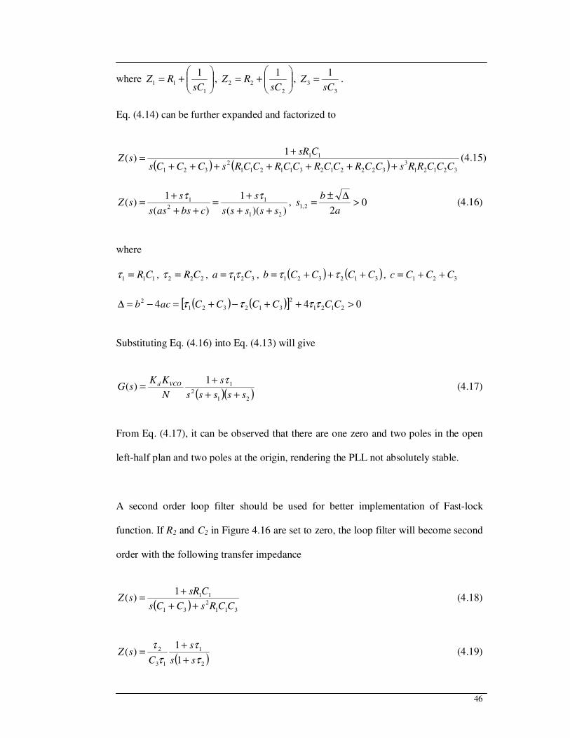
46
where
+=
1
11
1
sCRZ ,
+=
2
22
1
sCRZ ,
3
3
1
sCZ = .
Eq. (4.14) can be further expanded and factorized to
( ) ( ) 32121
3
322212311211
2
321
111)(
CCCRRsCCRCCRCCRCCRsCCCs
CsRsZ
+++++++
+= (4.15)
))((
1
)(
1)(
21
1
2
1
sssss
s
cbsass
ssZ
++
+=
++
+=
ττ, 0
22,1 >
∆±=
a
bs (4.16)
where
111 CR=τ , 222 CR=τ , 321 Ca ττ= , ( ) ( )312321 CCCCb +++= ττ , 321 CCCc ++=
( ) ( )[ ] 044 2121
2
312321
2 >++−+=−=∆ CCCCCCacb ττττ
Substituting Eq. (4.16) into Eq. (4.13) will give
( )( )21
2
11)(
sssss
s
N
KKsG VCOd
++
+=
τ (4.17)
From Eq. (4.17), it can be observed that there are one zero and two poles in the open
left-half plan and two poles at the origin, rendering the PLL not absolutely stable.
A second order loop filter should be used for better implementation of Fast-lock
function. If R2 and C2 in Figure 4.16 are set to zero, the loop filter will become second
order with the following transfer impedance
( ) 311
2
31
111)(
CCRsCCs
CsRsZ
++
+= (4.18)
( )2
1
13
2
1
1)(
τ
τ
τ
τ
ss
s
CsZ
+
+= (4.19)

47
where 111 CR=τ and
+=
31
3112
CC
CCRτ . The open loop gain Eq. (4.17) is redefined as
( )
+
+=
2
2
1
13
2
1
1)(
τ
τ
τ
τ
ss
s
CN
KKsG VCOd (4.20)
With s= jω, Eq. (4.20) can be expressed as
+
+−=
2
1
13
2
2
1
1)(
ωτ
ωτ
τω
τω
j
j
CN
KKjG VCOd (4.21)
Phase of G(jω) is given by
0
2
1
1
1 180)(tan)(tan)( −−= −− ωτωτωφ (4.22)
Phase margin is defined as
)(tan)(tan)( 2
1
1
1
arg ωτωτωφ −− −=inm (4.23)
In order to execute the Fast-lock function, resistor of the loop filter has to be resized.
Let n
RR 1'
1 = ,
n
1'
1
ττ = ,
n
2'
2
ττ = ,
−
= −−
2
'1
1
'1'' tantan)( τ
ωτ
ωωφ
nn (4.24)
To maintain constant phase margin as obtained from Eq. (4.21),
)(tan)(tan)(tantan)( 2
1
1
1
2
'1
1
'1'' ωτωτωφτ
ωτ
ωωφ −−−− −==
−
=
nn (4.25)

48
From Eq. (4.25), it shows that the loop bandwidth has been extended by n time
( ωω n=' ), resulting in the reduction of locking time by n times. In order to maintain
constant gain with extended bandwidth,
+
+−==
+
+−=
2
1
13
2
2
'
2
'
'
1
'
'
13
2'
'
2
'''
1
1)(
1
1)(
ωτ
ωτ
τω
τω
τω
τω
τω
τω
j
j
CN
KKjG
j
j
CN
KKjG VCOdVCOd (4.26)
where 22'
'
ωωdd KK
= , ddd KnKK 2
2
2'' ==
ω
ω. Hence, the conditions for bandwidth
extension are n
RR 1'
1 = , dd KnK2' = and ωω n=' .
Figure 4.17 illustrates the schematic of Loop Filter with Fast-lock function. “FL” is the
fast-lock function control switch that has to be connected to the chip’s “Fast-lock
Control” pin. For enhanced fast-lock performance, R2* should be shorted and C2*
should be opened. Otherwise, R2* and C2* can be optimized for enhanced noise
suppression capability.
C1
C3 C2*
R2* VI
n
R1
1)
11( R
n−
FL
Figure 4.17 Schematic of loop filter with Fast-lock function
Figure 4.18 shows the schematic of actual Loop Filter design which is used for PLL
locking simulation. The expected locking time for this fast-lock-incorporated loop
filter is 4 times shorter than normal loop filter without fast-lock function.

49
Figure 4.18 LP_Filter schematic
4.1.8 Fast-lock Control Switch
Fast-lock Timer Register has 12 bits, represented by FL0 (LSB) to FL11 (MSB)
(Table 4.2). When FLE is set to “1” and Fast-lock Timer Register has a non-zero
preset value, the fast-lock function will be activated. The Fast-lock Control switch will
be turned on, and Charge Pump will function at its maximum supply current of 3.2mA.
Once any of the registers (as listed in Table 4.2) is set, the Fast-lock Timer will start
counting the number of input-reference-signal pulses. When the number of pulses
fulfills the preset value, fast-lock function will be deactivated and Fast-lock Control
switch will be turned off, leaving the Charge Pump to function at the supply current
set by CP0, CP1 and CP2.
Assuming the preset value of Fast-lock Timer is FL and the period of Fast-lock Timer
is tFast-lock,
INREF
lockFastf
FLt
_
=− (4.27)

50
Figure 4.19 shows the design of Fast-lock Counter, which consists of 12-bit shift
register, 12-bit synchronous counter, comparator and reset function when counter is
full. Each bit counter design is as shown in Figure 4.3. Fast-lock Control Switch is an
analog switch that functions with Fast-lock Timer and external loop-filter by
connecting the “FL_Gnd” pin to external ground when the Fast-lock function is
activated.
Figure 4.19 Fast-lock Counter block diagram
Z-1
Z-1
12-bit shift register
+
12-bit synchronous counter +
Comparator DATA
REF_IN
Vdd
LE_FL
CLK
RESET0
Bit_CLK
Bit_Out Bit_Comp
12 12
D _Q
CDN
D Q
CDN
D Q
CDN
Vdd
RESET0
Vdd Vdd
RESET
FLE
FastLock
FLE
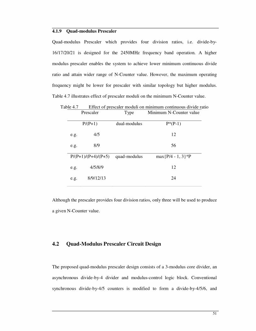
51
4.1.9 Quad-modulus Prescaler
Quad-modulus Prescaler which provides four division ratios, i.e. divide-by-
16/17/20/21 is designed for the 2450MHz frequency band operation. A higher
modulus prescaler enables the system to achieve lower minimum continuous divide
ratio and attain wider range of N-Counter value. However, the maximum operating
frequency might be lower for prescaler with similar topology but higher modulus.
Table 4.7 illustrates effect of prescaler moduli on the minimum N-Counter value.
Table 4.7 Effect of prescaler moduli on minimum continuous divide ratio
Prescaler Type Minimum N-Counter value
P/(P+1) dual-modulus P*(P-1)
e.g. 4/5 12
e.g. 8/9 56
P/(P+1)/(P+4)/(P+5) quad-modulus maxP/4 - 1, 3*P
e.g. 4/5/8/9 12
e.g. 8/9/12/13 24
Although the prescaler provides four division ratios, only three will be used to produce
a given N-Counter value.
4.2 Quad-Modulus Prescaler Circuit Design
The proposed quad-modulus prescaler design consists of a 3-modulus core divider, an
asynchronous divide-by-4 divider and modulus-control logic block. Conventional
synchronous divide-by-4/5 counters is modified to form a divide-by-4/5/6, and
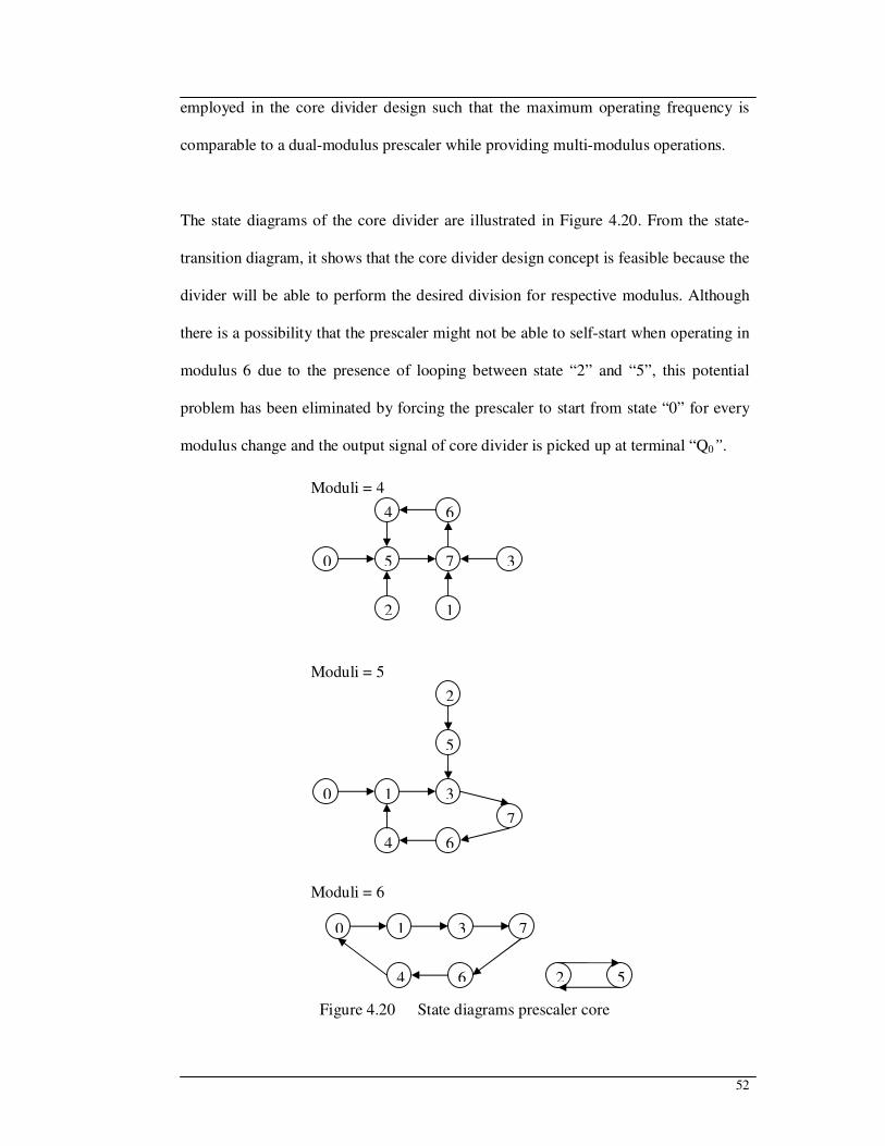
52
employed in the core divider design such that the maximum operating frequency is
comparable to a dual-modulus prescaler while providing multi-modulus operations.
The state diagrams of the core divider are illustrated in Figure 4.20. From the state-
transition diagram, it shows that the core divider design concept is feasible because the
divider will be able to perform the desired division for respective modulus. Although
there is a possibility that the prescaler might not be able to self-start when operating in
modulus 6 due to the presence of looping between state “2” and “5”, this potential
problem has been eliminated by forcing the prescaler to start from state “0” for every
modulus change and the output signal of core divider is picked up at terminal “Q0”.
Figure 4.20 State diagrams prescaler core
4 6
5 70 3
2 1
Moduli = 4
2
5
31
4 6
7
0
Moduli = 5
0 1 3 7
4 6 2 5
Moduli = 6

53
MOD_A and MOD_B are the control signals from N-Counter, which are used to
control the division ratio of the prescaler according to the setting listed in Table 4.8.
Table 4.8 Moduli-control pins setting
MOD_B MOD_A Division ratio
0 0 4*4 = 16
0 1 (4*3) + 5 = 17
1 0 5*4 = 20
1 1 (5*3) + 6 = 21
Figure 4.21 shows the design of quad-modulus prescaler which consists of a core
divide-by-4/5/6 divider operating at highest frequency, an asynchronous divide-by-4
divider, a high frequency input buffer, a differential-to-single-ended output buffer and
modulus-control logic block.
Figure 4.21 Div16172021_top diagram
Div-by 4/5/6
IN_p
IN_n
Div-by 2
Div-by 2
presc_OUT Modulus-control logic
MOD_A
MOD_B
SA
_SA
SB _SB
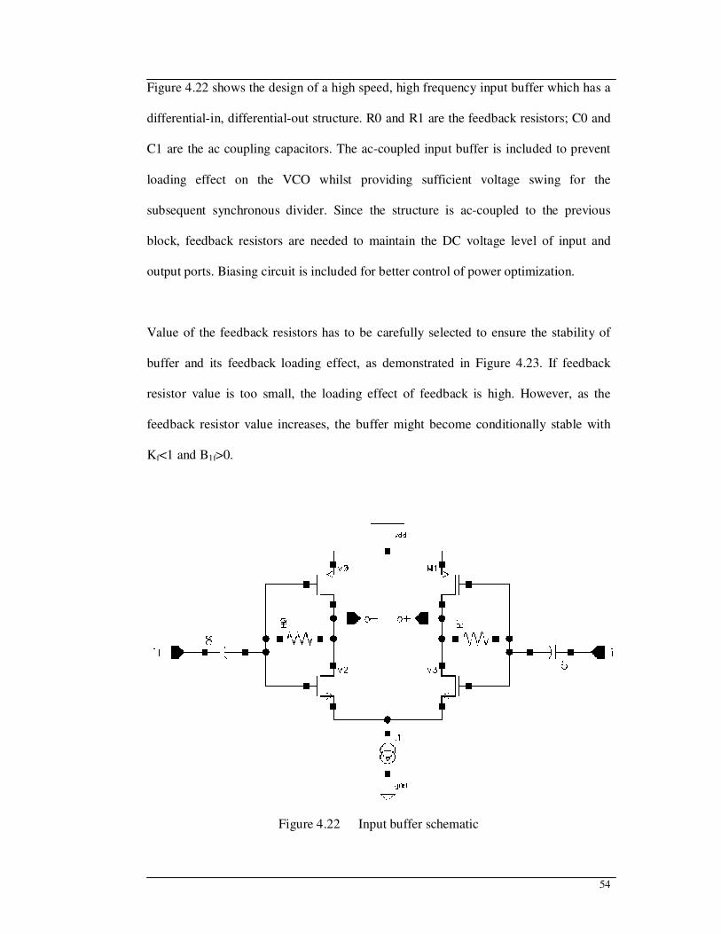
54
Figure 4.22 shows the design of a high speed, high frequency input buffer which has a
differential-in, differential-out structure. R0 and R1 are the feedback resistors; C0 and
C1 are the ac coupling capacitors. The ac-coupled input buffer is included to prevent
loading effect on the VCO whilst providing sufficient voltage swing for the
subsequent synchronous divider. Since the structure is ac-coupled to the previous
block, feedback resistors are needed to maintain the DC voltage level of input and
output ports. Biasing circuit is included for better control of power optimization.
Value of the feedback resistors has to be carefully selected to ensure the stability of
buffer and its feedback loading effect, as demonstrated in Figure 4.23. If feedback
resistor value is too small, the loading effect of feedback is high. However, as the
feedback resistor value increases, the buffer might become conditionally stable with
Kf<1 and B1f>0.
Figure 4.22 Input buffer schematic

55
Figure 4.23 Effect of feedback resistor on buffer stability
1kΩ
5kΩ
10kΩ
1kΩ
5kΩ
10
kΩ

56
Figure 4.24 shows the core divider design that consists of three synchronous DFF
which are constructed to form a divide-by-4/5/6 divider. SA and SB are the control
pins for selecting the division ratio of the core divider. Although the three dividers are
operating at the highest frequency, total power consumption can be reduced with
proper sizing of transistors and implementation of biasing circuit.
Figure 4.24 Div456_top block diagram
Table 4.9 shows the settings for div456_top which correspond to respective divide
ratios.
Table 4.9 Control logic for divide-by-4/5/6
SB SA Divide ratio
1 1 4
1 0 5
0 0 6
When both SA and SB are at logic “1”, the inverse output of third DFF (i.e. _Q2) will
remain at “0” and the output frequency of core divider is determined by the first 2
DFFs, which forms a divide-by-4 divider.
D Q1
_Q1
D1 Q0
D2 _Q0
D1 Q2
D2 _Q2
div456_out SA
SB
clk

57
When SB is at logic “1” but SA is at logic “0”, the loop will be momentarily closed
over the 3 DFFs. When Q0=Q1=0, _Q1=_Q2=1 and a “1” will be injected to the first
DFF, causing a delay which is equivalent to a divide-by-5 operation. When both SA
and SB are at logic “0”, the 3 DFFs will form a divide-by-6.
Differential-signal-pair concept is implemented throughout the entire architecture
instead of the usual single-ended structure because the former provides immunity
towards common-mode noise, supply voltage variation and fabrication process
variation. Figure 4.25 shows the current mode logic (CML) latch which is used for
constructing the master-slave DFFs in the divider. This topology is opted for the
various advantages which it offers as compared to conventional CMOS static circuit.
Figure 4.25 CML latch schematic

58
The propagation delay (D), dynamic power dissipation (P), power delay (PD) and
energy delay (ED) of CML structure is given by [42]
I
VCNNRCDCML
∆∗∗== (4.28)
ddCML VINP ∗∗= (4.29)
ddddCML VVCNI
VNCNIVPD ∗∆∗∗=
∆∗= 2 (4.30)
( ) ( ) ( )I
VVCN
I
VNVVVCNED dd
ddCML
2232 ∆
=∆
∗∆= (4.31)
where N is the number of identical gate, C is the load capacitance, I is the biasing
current and ∆V (=I*R) is the output voltage swing. According to the equations, CML
latches can be optimized by reducing the supply voltage, reducing signal voltage
swing and/or increasing biasing current.
The constant current drawn by the source-coupled transistors in CML can suppress the
common-mode noise which is caused by current spikes during switching. The
differential-signal pair in CML also minimizes the injection of current into substrate
and reduces switching noise significantly. Besides, the low input voltage swing
requirement also improves the circuit’s input sensitivity and enables the circuit to
function at higher speed due to shorter toggle time.
The core divider has to function at the highest speed possible but the major bottleneck
is the gates in the core divider loop. Figure 4.26 shows the implementation of CML
with embedded OR-gate. This topology minimizes the delay and power consumption
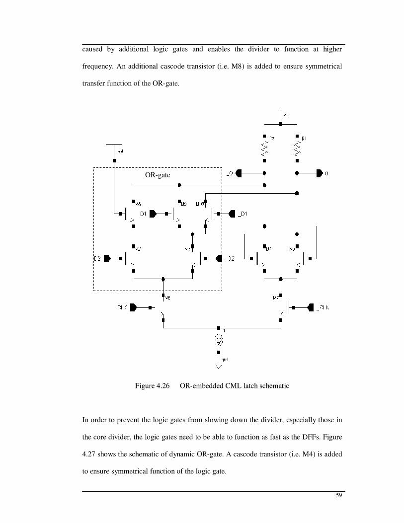
59
caused by additional logic gates and enables the divider to function at higher
frequency. An additional cascode transistor (i.e. M8) is added to ensure symmetrical
transfer function of the OR-gate.
Figure 4.26 OR-embedded CML latch schematic
In order to prevent the logic gates from slowing down the divider, especially those in
the core divider, the logic gates need to be able to function as fast as the DFFs. Figure
4.27 shows the schematic of dynamic OR-gate. A cascode transistor (i.e. M4) is added
to ensure symmetrical function of the logic gate.
OR-gate

60
Figure 4.27 OR gate schematic
Subsequent asynchronous divide-by-4 divider also utilizes the same DFF topology but
the sizing of the MOSFETS and current consumptions for the dividers and logic gates
were optimized because the asynchronous dividers are functioning at lower frequency.
Modulus-control-logic is integrated to control the timing for modulus change after
MOD_A or/and MOD_B is changed. The mode-control signals will be latched and
held by the DFFs during the falling edge of output signal, and passed to the circuit
during subsequent rising edge of the output signal.

61
4.3 Frequency Synthesizer and Prescaler Layout
The layout view for fractional-N frequency synthesizer is illustrated in Figure 4.28.
The entire design occupied an area of approximately 0.699mm2.
Figure 4.28 Layout view of fractional-N frequency synthesizer

62
Figure 4.29 shows the layout view for quad-modulus prescaler. The size of the
prescaler is approximately 0.102mm2.
Figure 4.29 Layout view of quad-modulus prescaler
4.4 Design Specifications
Table 4.10 shows the power supply specification for PLL. The minimum and
maximum values for the supply current were obtained from the transient simulation
results of 45 corners.

63
Table 4.10 Power supply specification for PLL
Value Parameter Symbol Conditions
Min Typ Max
Supply voltage Vdd (V) 3.0 3.3 3.6
Supply current Idd (mA) Without Prescaler
and Charge Pump
0.4 0.6 0.9
Table 4.11 shows the number of bits and range of the counters, timer and registers.
The values are stored in binary code.
Table 4.11 Parameters of PLL counters, timer and registers
Value Building block Bits
Min Max
R-Counter 4 1 15
Fast-lock Timer 12 0 4095
N-Counter 9 64 511
FN Register 9 0 511
FD Register 9 1 511
Interface Register 2 0 3
Mode Register 6 0 63
Table 4.12 shows the theoretical frequency range of the frequency synthesizer using
ideal prescaler. Based on this design topology, the ideal synthesizer is capable of
functioning from 1675MHz till 12724.95MHz when operating in the 2450MHz
frequency band (with reference frequency of 25MHz and channel spacing of 50kHz),
and functioning from 700MHz till 10179.95MHz when operating in the 910MHz
frequency band (with reference frequency of 20MHz and channel spacing of 50kHz).

64
However, the actual attainable maximum frequency will be restricted by the
performances of counters, VCO and prescaler.
Table 4.12 Theoretical frequency range of frequency synthesizer
Band
(MHz)
Reference
(MHz)
Modulus P Channel
spacing
(kHz)
Min Frequency
(MHz)
Max Frequency
(MHz)
2450 25 16/17/20/21 50 1675.00 12724.95*
910 20 8/9/12/13 50 700.00 10179.95*
* The actual frequency range might be narrower, depending on the performances of
counters, VCO and prescaler.
Table 4.13 shows the timing specifications of the frequency synthesizer settings,
which includes the setup time, rise/fall time, hold time, and pulse width of
PLL_DATA, PLL_CLK and PLL_LE signals.
Table 4.13 Specifications for timing diagram of frequency synthesizer settings
Symbol Min (ns)
Typ (ns)
Max (ns)
PLL_DATA/PLL_CLK Setup Time tdcs 10 - -
PLL_DATA/PLL_CLK Hold Time tdch 10 - -
PLL_CLK Rising Edge tcr - - 100
PLL_CLK Falling Edge tcf - - 100
PLL_CLK Width (High) tcwh 10 - -
PLL_CLK Width (Low) tcwl 10 - -
PLL_CLK/PLL_LE Setup Time tcls 10 - -
PLL_LE Rising Edge tlr - - 100
PLL_LE Falling Edge tlf - - 100
PLL_LE Pulse Width tlw 10 - -

65
4.5 PC Program for PLL Frequency Synthesizer Setting
A program was written for adjusting the PLL frequency synthesizer setting through
parallel port of PC with the aid of Visual C++ 6.0 compiler.
4.5.1 User Interface
There are three available user interfaces. Figure 4.30 and Figure 4.31 show the first
two interfaces: the former displays the bit-numbers and the latter displays the values of
respective counters. The switching between two interfaces can be executed by
depressing “I” or “l” key. The green-colour alphabets represent the letters to be
depressed in order to invoke respective predefined functions or input menu of
parameters.
Figure 4.30 Main user interface for synthesizer setting

66
Figure 4.31 Second user interface for synthesizer setting
Figure 4.32 shows the third user interface which contains the “Help” information. This
page can be invoked by depressing “H” key and revoked by depressing any random
key.
Figure 4.32 Third user interface displaying “Help” information

67
4.5.2 Hardware Interface
The parallel port found on PC may provide +3.3V or +5.0V interface voltage for PLL
frequency synthesizer setting but the chip-under-test might require a lower interface
voltage. A high-to-low level shifter from Philips Semiconductors (74HC4050) is used
to bridge the chip and parallel port. Power supply voltage of the chip is used as a
reference level by the level shifter to convert the parallel port voltage accordingly for
smooth interfacing. Figure 4.33 shows the assigned parallel port pins which will
output PLL_DATA, PLL_CLK and PLL_LE signals respectively.
Figure 4.33 PLL setting through parallel port

68
CHAPTER 5
SIMULATION AND MEASUREMENT RESULTS
5.1 Testbenches
Figure 5.1 shows the PLL locking simulation testbench and Figure 5.2 shows the top-
level fractional-N frequency synthesizer testbench.
Figure 5.1 PLL locking simulation testbench

69
Figure 5.2 Top level simulation testbench

70
5.1.1 Counters
Figures 5.3-5.10 show the testbenches for counters functionality tests and their
respective transient simulation results.
Figure 5.3 Testbench for AB_Counter functionality test

71
Figure 5.4 Transient simulation results of AB_Counter

72
Figure 5.5 Testbench for C_Counter functionality test

73
Figure 5.6 Transient simulation results of C_Counter

74
Figure 5.7 Testbench for N_Counter functionality test

75
Figure 5.8 Transient simulation results of N_Counter

76
Figure 5.9 Testbench for R_Counter functionality test

77
Figure 5.10 Transient simulation results of R_Counter
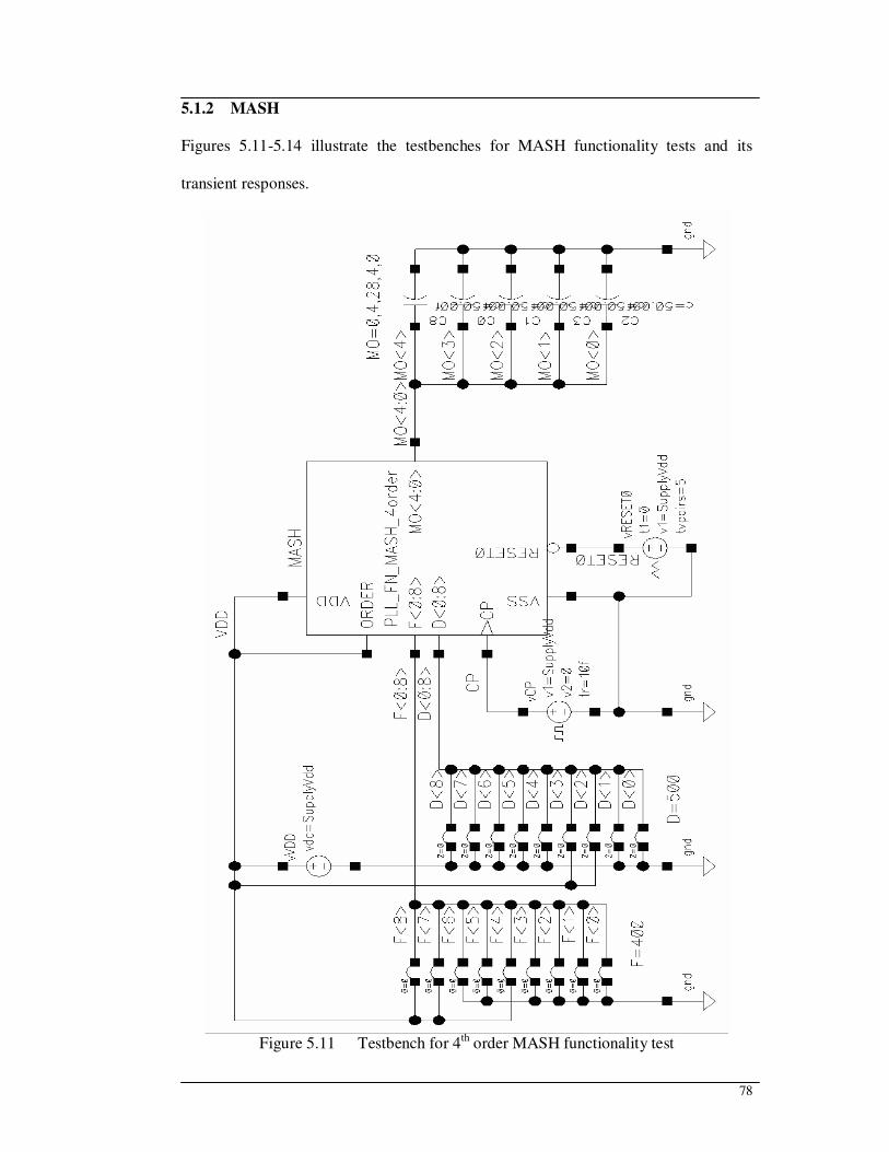
78
5.1.2 MASH
Figures 5.11-5.14 illustrate the testbenches for MASH functionality tests and its
transient responses.
Figure 5.11 Testbench for 4th order MASH functionality test

79
Figure 5.12 Transient simulation result of MASH_4order
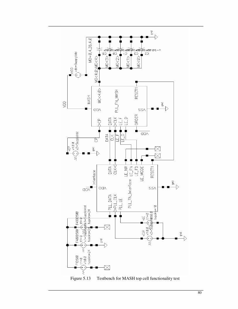
80
Figure 5.13 Testbench for MASH top cell functionality test

81
Figure 5.14 Transient response of MASH top cell

82
5.1.3 Interface
Figure 5.15 shows the testbench for Interface functionality test and the results are
shown in Figure 5.16.
Figure 5.15 Testbench for Interface functionality test

83
Figure 5.16 Transient simulation results of Interface

84
5.1.4 Mode Register
Figure 5.17 shows the simulation setups for testing the functionality of Mode Register
and Figure 5.18 shows its transient simulation results.
Figure 5.17 Testbench for Mode Register functionality test
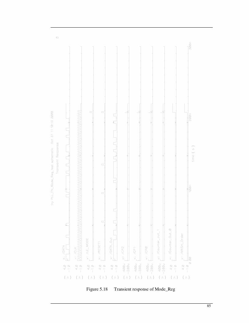
85
Figure 5.18 Transient response of Mode_Reg

86
5.1.5 Fastlock
Figure 5.19 demonstrates the testbench for Fastlock functionality test and the
simulation results is as shown in Figure 5.20.
Figure 5.19 Testbench for Fastlock Counter functionality test

87
Figure 5.20 Transient response of Fastlock_Counter
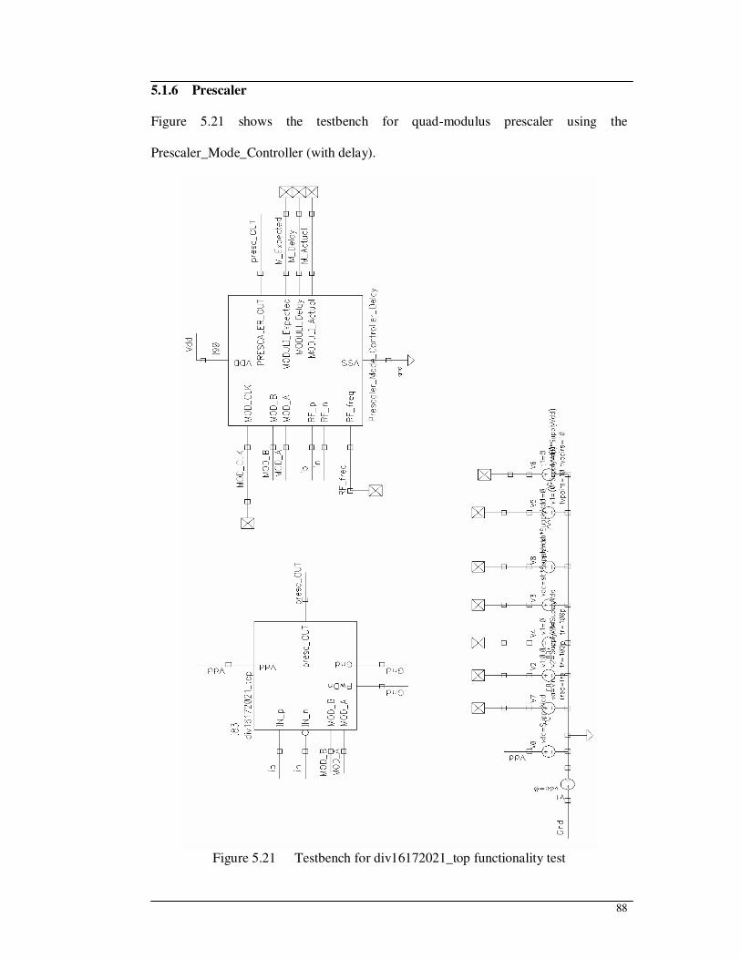
88
5.1.6 Prescaler
Figure 5.21 shows the testbench for quad-modulus prescaler using the
Prescaler_Mode_Controller (with delay).
Figure 5.21 Testbench for div16172021_top functionality test

89
5.2 Simulation Results
Simulations for the proposed frequency synthesizer design were carried out in
Cadence IC5.1.41 under Red Hat Enterprise Linux WS release 4 (Nahant Update 4).
5.2.1 Prescaler
Prescaler has a minimum input signal voltage amplitude requirement for the circuit to
function properly. The performance of prescaler with various differential input signal
amplitudes was simulated. Figure 5.22 shows the simulation results at Typical
condition (TT, 3.3V, 250C). It was observed that the input sensitivity of the proposed
prescaler design was very high with minimum differential input signal amplitude
required of 350mV.
100 200 300 400 500 600 700 800 900 1000 1100
12
13
14
15
16
17
18
19
20
21
22
Mod
ulu
s
Differential Amplitude (V)
16
17
20
21
Figure 5.22 Minimum input signal amplitude requirement for prescaler
The operating ranges of prescaler, simulated at 100MHz-step increments, were
obtained with the help of Verilog-A view of PLL_FN_Prescaler_mode_controller. At
Typical condition (TT, 3.3V, 250C), the prescaler was able to function up till 3.87GHz
with ac current consumption of 21.09mA and functioned up till 3.05GHz with ac

90
current consumption of 18.09mA. Table 5.1 shows the process corners simulation
results of the prescaler with supply current of 18.09mA (at Typical condition).
Table 5.1 Operating ranges of prescaler in 45 cases
Temp.
(0C)
Maximum operating frequency
(GHz)
Process corner Vdd
(V)
Schematic
(30fF parasitic capacitors)
Extracted_C
FF 3.0 25 3.00 3.00
FF 3.0 -40 3.00 3.00
FF 3.0 90 3.00 2.95
FF 3.3 25 3.00 3.00
FF 3.3 -40 3.00 3.00
FF 3.3 90 3.00 2.95
FF 3.6 25 3.00 3.00
FF 3.6 -40 3.00 3.00
FF 3.6 90 3.00 3.00
FS 3.0 25 3.00 3.00
FS 3.0 -40 3.00 3.00
FS 3.0 90 2.95 2.95
FS 3.3 25 3.00 3.00
FS 3.3 -40 3.00 3.00
FS 3.3 90 2.95 2.95
FS 3.6 25 3.00 3.00
FS 3.6 -40 3.00 3.00
FS 3.6 90 3.00 3.00

91
Temp.
(0C)
Maximum operating frequency
(GHz)
Process corner Vdd
(V)
Schematic
(30fF parasitic capacitors)
Extracted_C
SF 3.0 25 3.00 2.90
SF 3.0 -40 3.00 3.00
SF 3.0 90 2.85 2.75
SF 3.3 25 3.00 2.95
SF 3.3 -40 3.00 3.00
SF 3.3 90 2.80 2.75
SF 3.6 25 3.00 2.95
SF 3.6 -40 3.00 3.00
SF 3.6 90 2.80 2.80
SS 3.0 25 3.00 2.90
SS 3.0 -40 3.00 3.00
SS 3.0 90 2.90 2.80
SS 3.3 25 3.00 2.95
SS 3.3 -40 3.00 3.00
SS 3.3 90 2.80 2.75
SS 3.6 25 3.00 2.95
SS 3.6 -40 3.00 3.00
SS 3.6 90 2.80 2.80
TT 3.0 25 3.00 3.00
TT 3.0 -40 3.00 3.00
TT 3.0 90 2.85 2.85

92
Temp.
(0C)
Maximum operating frequency
(GHz)
Process corner Vdd
(V)
Schematic
(30fF parasitic capacitors)
Extracted_C
TT 3.3 25 3.05 3.05
TT 3.3 -40 3.00 3.00
TT 3.3 90 2.90 2.90
TT 3.6 25 3.00 3.00
TT 3.6 -40 3.00 3.00
TT 3.6 90 2.90 2.90
5.2.2 Frequency Synthesizer Current Consumption
Table 5.2 Current consumptions of synthesizer building blocks at Typical conditions (TT, 3.3V, 250C, 2450.05MHz)
Building block Current
MASH 1.66 mA
N-Counter 1.22 mA
R-Counter 15.64 µA
FL Counter 88.01 µA
Counter_Out 153.28 µA
Interface 0.58 nA
PFD 115.32 µA
Prescaler 18.09 mA
Total 21.34 mA
In order to investigate the performance of the fractional-N frequency synthesizer,
simulations were being carried out in all 45 cases which consisted of combinations

93
from five process corners (Typical (TT); Slow-Slow (SS); Fast-Fast (FF); Slow-Fast
(SF); Fast-Slow (FS)), three supply voltages (3.0V; 3.3V; 3.6V) and three
temperatures (-400C; 250C, 900C). The average ac current consumptions of the digital
circuits are measured over the period from 1µs to 3µs, and tabulated in Table 5.2.
Figure 5.23 shows the current consumption of MASH and Table 5.3 lists summary of
the average current consumptions for synthesizer building blocks in all 45 cases.
1.20
1.30
1.40
1.50
1.60
1.70
1.80
1.90
2.00
2.10
2.20
Cases
Cu
rre
nt
(mA
)
Figure 5.23 Current consumption of MASH in 45 cases
Table 5.3 Average current consumptions of synthesizer building blocks in 45
cases
Current Building block
Maximum Average Minimum
MASH 2.14 1.69 1.38 mA
N-Counter 1.56 1.23 0.97 mA
R-Counter 21.50 15.86 11.61 µA
FL Counter 117.78 89.65 69.15 µA
Counter_Out 228.06 155.71 101.39 µA
Interface 50.38 5.94 0.26 nA
PFD 143.26 115.96 93.95 µA
Total 4.21 3.30 2.62 mA

94
5.2.3 PLL Settings
With a crystal oscillator of 25MHz, the typical values for counters, registers and timer
are as shown in Table 5.4.
Table 5.4 Typical values of counters, registers and timer (crystal oscillator frequency= 25MHz)
Building block Value Note
R-Counter 1 Reference frequency= 25MHz
N-Counter 98 LO frequency= 2450.05MHz
FN Register 1
FD Register 500
MASH order 1 MASH order=4
Counter_Out 1 Prescaler output will be transmitted to
“Counter_Out”pin
Charge Pump current 0 Charge Pump current= 200µA
Fast-lock Timer 20 Initial value of Fast-lock Timer= 20µs
Figure 5.24 shows the timing diagram of PLL setting which was generated by the
Verilog-A view of PLL_FN_setting.
Figure 5.24 Timing diagram of PLL setting

95
5.2.4 Prescaler Controller
Prescaler Controller was used to test the dynamic characteristic of prescaler in a more
efficient manner. The desired modulus waveform, actual modulus waveform and their
discrepancies were plotted. Figure 5.25 shows an example of the test results at Typical
condition (TT, 3.3V, 250C) with 50MHz-step increments in schematic view.
Figure 5.25 Dynamic characteristic of prescaler at Typical condition

96
According to the graphs, the prescaler functioned properly for operating frequency
below 3500MHz and errors were detected in the division ratios for operating
frequency beyond 3450MHz.
Although there were 12 modulus-changing patterns, not all were involved in the
2450MHz frequency band operations. For operating frequency= 2400~2500MHz with
step size= 50kHz and MASH order= 3 or 4, the 8 modulus-changing patterns involved
were: 1617, 1716, 1620, 2016, 2116, 1621, 2120, 2117 while the
following 4 modulus-changing patterns were not involved: 1720, 2021, 2017,
1721, as illustrated in Figure 5.26.
16 17
2021
16 17
2021 X
X X
Figure 5.26 Modulus-changing patterns in 2450MHz band
If the design specifications for prescaler are very stringent, the ability to switch
between uninvolved modulus-changing patterns may be ignored. However, this will
limit the usable range of the prescaler.
5.2.5 N-Counter and MASH
The pulse interval of N-Counter output in Typical condition (TT, 3.3V, 250C) at
2450.05MHz and MASH order= 4 is shown in Figure 5.27. The pseudo-random
number for pulse interval was controlled by the MASH.

97
35
36
37
38
39
40
41
42
43
1 5 9 13 17 21 25 29 33 37 41 45 49 53 57 61 65
Cycle
Pu
lse
In
terv
al
(ns
)
Figure 5.27 Pulse interval of N-Counter output
The division ratio of FN over FD was simplified by using greatest common divisor
(GCD) method. Figure 5.28 illustrates the GCD value calculated via method of
exhaustion. Upon obtaining the GCD value, the respective period of pseudo-random
series was determined from Table 5.5.
Figure 5.28 Greatest common divisor of FN and FD
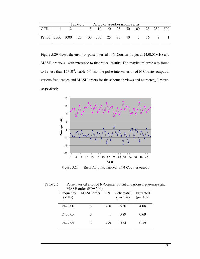
98
Table 5.5 Period of pseudo-random series
GCD 1 2 4 5 10 20 25 50 100 125 250 500
Period 2000 1000 125 400 200 25 80 40 5 16 8 1
Figure 5.29 shows the error for pulse interval of N-Counter output at 2450.05MHz and
MASH order= 4, with reference to theoretical results. The maximum error was found
to be less than 15*10-4
. Table 5.6 lists the pulse interval error of N-Counter output at
various frequencies and MASH orders for the schematic views and extracted_C views,
respectively.
-20
-15
-10
-5
0
5
10
15
1 4 7 10 13 16 19 22 25 28 31 34 37 40 43
Case
Err
or
(pe
r 1
0k
)
Figure 5.29 Error for pulse interval of N-Counter output
Table 5.6 Pulse interval error of N-Counter output at various frequencies and
MASH order (FD= 500)
Frequency
(MHz)
MASH order FN Schematic
(per 10k)
Extracted
(per 10k)
2420.00 3 400 6.60 4.08
2450.05 3 1 0.89 0.69
2474.95 3 499 0.54 0.39

99
2420.00 4 400 6.97 4.25
2450.05 4 1 7.08 4.22
2474.95 4 499 6.79 4.30
According to Table 5.6, the error for pulse interval of N-Counter output at various
frequencies was observed to be relatively smaller for 3rd
order MASH.
Figure 5.30 illustrates the theoretical noise shift characteristic of MASH at FN= 1,
FD=500 and REFf = 25MHz. Figure 5.31 shows the noise level of PDF output at
6.25kHz with REFf =25MHz. It was observed that 4th
order MASH had the best noise-
suppressing capability at low frequency, and the differences between noise levels of
adjacent MASH orders were around 56dB.
Figure 5.30 Noise shift characteristic of MASH

100
Figure 5.31 Noise level of PFD output at 6.25kHz ( REFf = 25MHz)
5.2.6 Modulus Control
In this design, MOD_A and MOD_B were the control lines for switching the modulus
of prescaler. Both lines had delay in terms of nanosecond, which was taken into
consideration during the design phase of prescaler. Figure 5.32 and Figure 5.33 show
the delay of MOD_A and MOD_B, respectively, in all 45 cases.
0.00
0.50
1.00
1.50
2.00
2.50
3.00
3.50
1 4 7 10 13 16 19 22 25 28 31 34 37 40 43
Case
MO
D_
A D
ela
y (
ns)
Minimum
Maximum
Figure 5.32 Delay of MOD_A in 45 cases

101
0.00
0.50
1.00
1.50
2.00
2.50
3.00
1 4 7 10 13 16 19 22 25 28 31 34 37 40 43
Case
MO
D_
B D
ela
y (
ns
)
Minimum
Maximum
Figure 5.33 Delay of MOD_B in 45cases
5.2.7 PFD and Charge Pump
Figure 5.34 Intercept of charge pump current in Typical condition

102
The intercept of charge pump current is a vital parameter for approximating the
linearity of charge pump and PFD. Hence, its absolute value was kept to be as small as
possible when the LO signal was synchronous with the reference signal. Figure 5.34
illustrates the intercept of charge pump current at various loop filter voltages (i.e., 0V
to 3.3V) in Typical condition (TT, 3.3V, 250C). Figure 5.35 demonstrates the intercept
of charge pump current at various loop filter voltages in 45 cases, showing optimal
performance when loop filter voltage is within the range of (0.1*Vdd) to (0.8*Vdd).
Figure 5.35 Intercept of charge pump current in 45 cases
Linearity of charge pump current is another key issue which needs to be addressed,
especially when the PLL is locked. Figure 5.36 and Figure 5.37 show the linearity of

103
charge pump current with PFD at Typical condition (TT, 3.3V, 250C). According to
the figure, PFD and Charge Pump functioned optimally when loop filter voltage was
within the range of (0.1*Vdd) to (0.8*Vdd), and the linearity was degenerated when
loop filter voltage was adjacent to supply voltages. The period of the linearity curve
was less than 2π because two delay cells were implemented to remove the dead-zone
in PFD and Charge Pump.
Figure 5.36 Linearity of charge pump current with PFD at Typical condition
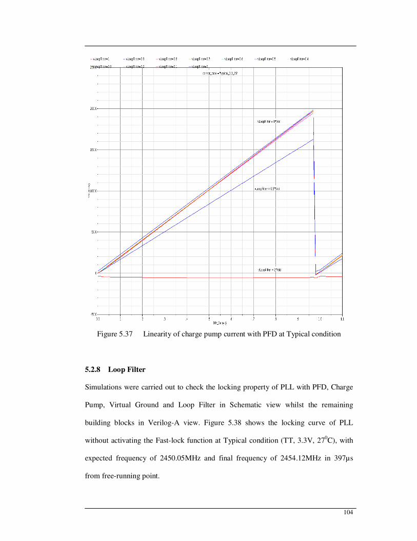
104
Figure 5.37 Linearity of charge pump current with PFD at Typical condition
5.2.8 Loop Filter
Simulations were carried out to check the locking property of PLL with PFD, Charge
Pump, Virtual Ground and Loop Filter in Schematic view whilst the remaining
building blocks in Verilog-A view. Figure 5.38 shows the locking curve of PLL
without activating the Fast-lock function at Typical condition (TT, 3.3V, 270C), with
expected frequency of 2450.05MHz and final frequency of 2454.12MHz in 397µs
from free-running point.

105
Figure 5.38 Locking curve of PLL without Fast-lock function at Typical condition
Figure 5.39 shows the PLL locking curve with Fast-lock Timer set at 20µs at Typical
condition (TT, 3.3V, 270C). The expected frequencies monitored were 2474.95MHz,
2450.05MHz and 2420.00MHz, respectively. According to the simulation results, PLL
was found to be able to lock faster upon activation of Fast-lock function.
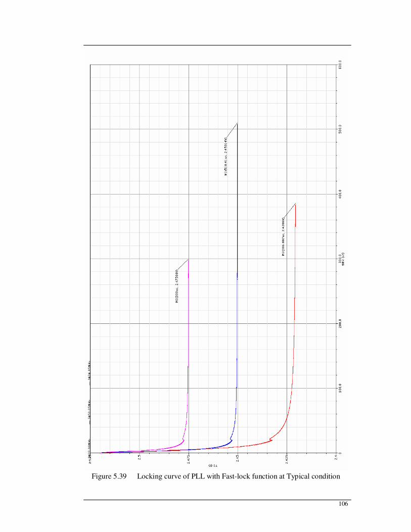
106
Figure 5.39 Locking curve of PLL with Fast-lock function at Typical condition

107
Figure 5.40 shows the responses of synthesizer when frequency jumped from
2400MHz to 2500MHz and vice versa at Typical condition (TT, 3.3V, 270C), with the
Fast-lock Timer set at 30µs. Frequency ripple was caused by the inherently inconstant
division ratio of N-Counter, due to MASH, as depicted by Figure 5.41. The ripple had
a period of around 40ns which was comparable to the period of 25MHz reference
signal, and amplitude of less than 300Hz which could be further reduced via narrow-
bandwidth loop filter. This 300Hz ripple was identified to be 0.125ppm of the
2400MHz center frequency.
Figure 5.40 Synthesizer responses to frequency jumps

108
Figure 5.41 Frequency ripple of synthesizer

109
5.3 Measurement Results
The frequency synthesizer design was taped-out for facilitating the study of its actual
performance. Five samples were obtained, and the performances of frequency
synthesizer were measured with an integrated VCO that is designed for 2450MHz
frequency band operation.
5.3.1 Test Plan
Table 5.7 shows the test conditions whilst Table 5.8 lists the measurement equipments
used for measuring the performances of frequency synthesizer.
Table 5.7 Test conditions for frequency synthesizer
Parameter Unit Test condition
PLL current consumption mA Vdd= 3.0; 3.3; 3.6V
Charge Pump current consumption µA Vdd= 3.0; 3.3; 3.6V
Operating frequency range MHz Vdd= 3.0; 3.3; 3.6V
Span= 1MHz for 2450MHz;
100kHz for 25MHz
Table 5.8 Measurement equipments list
Description Manufacturer Model Quantity
22GHz Microwave Spectrum Analyzer HP 8593E 1
9kHz~2.9GHz Spectrum Analyzer HP 8594E 1
BenchLink Spectrum Analyzer Agilent E4444A 1
USB/GPIB Interface Agilent
Technologies
82357A 1
DC Power Supply KENWOOD 1
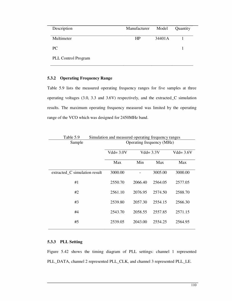
110
Description Manufacturer Model Quantity
Multimeter HP 34401A 1
PC 1
PLL Control Program
5.3.2 Operating Frequency Range
Table 5.9 lists the measured operating frequency ranges for five samples at three
operating voltages (3.0, 3.3 and 3.6V) respectively, and the extracted_C simulation
results. The maximum operating frequency measured was limited by the operating
range of the VCO which was designed for 2450MHz band.
Table 5.9 Simulation and measured operating frequency ranges
Operating frequency (MHz)
Vdd= 3.0V Vdd= 3.3V Vdd= 3.6V
Sample
Max Min Max Max
extracted_C simulation result 3000.00 - 3005.00 3000.00
#1 2550.70 2066.40 2564.05 2577.05
#2 2561.10 2076.95 2574.50 2588.70
#3 2539.80 2057.30 2554.15 2566.30
#4 2543.70 2058.55 2557.85 2571.15
#5 2539.05 2043.00 2554.25 2564.95
5.3.3 PLL Setting
Figure 5.42 shows the timing diagram of PLL settings: channel 1 represented
PLL_DATA, channel 2 represented PLL_CLK, and channel 3 represented PLL_LE.

111
Figure 5.42 Timing diagram for PLL setting
5.3.4 Reference Spurs
Reference spur is one of the most common contributors to the spurious levels on the
PLL output spectrum. These spurs can be observed at an offset of REFf± from the
PLL output frequency, and are instigated by the non-idealities in PLL components,
namely:
• leakage current in VCO tuning node
• mismatch in PFD and Charge Pump propagation delay
• mismatch in CP current, and charge injection.
Table 5.10 summarizes the reference spurious levels at REFf with carrier frequency set
at 2450MHz and operating voltage of 3.3V. Figures 5.43-5.45 show the reference spur

112
plots for Sample #5. Reference spur plots for Samples #1-#4 are attached in Appendix
A.
Table 5.10 Frequency synthesizer reference spurs
Spurious level (dBc) Sample
at 10.80MHz_left at 25.05MHz_right at 25.80MHz_left
#1 -61.98 -71.10 -68.89
#2 -62.45 -71.82 -69.41
#3 -63.08 -71.61 -69.26
#4 -62.14 -71.43 -69.42
#5 -62.82 -71.38 -70.26
Figure 5.43 #5 frequency synthesizer reference spur plot at ~25MHz offset (right)
Figure 5.44 #5 frequency synthesizer reference spur plot at 10.80MHz offset (left)
RBW= 10kHz
VBW= 3kHz
Span= 60MHz
Sweep= 6s
MASH= 3
Moduli= 500
RBW= 10kHz
VBW= 3kHz
Span= 60MHz
Sweep= 6s
MASH= 3
Moduli= 500

113
Figure 5.45 #5 frequency synthesizer reference spur plot at ~25MHz offset (left)
5.3.5 Fractional Spurs
Fractional spurs can be observed at spacings equal to the channel spacing, i.e. 50kHz,
of the synthesizer. This phenomenon could be due to the following:
• inability of modulator to adequately correlate the output samples, especially for
inputs which are close to integer value
• non-linear mixing in PFD generates down-conversion of tones which are
intrinsically present around 2REFf .
Figure 5.46 Fractional spurious levels at 2462.5MHz and 2463.3MHz
Fractional Spurious
-66
-65
-64
-63
-62
-61
-60
-59
-58
25 45 65 85
Offset (MHz)
Sp
ur
lev
el (d
Bc
)
#5 (2462.5MHz)
#5 (2463.3MHz)
Ref = 10dBm
Attn = 20dB
RBW = 1MHz
VBW = 300kHz
Sweep = 5s
Span = 150MHz
RBW= 10kHz
VBW= 3kHz
Span= 60MHz
Sweep= 6s
MASH= 3
Moduli= 500

114
Figure 5.46 shows the comparison of fractional spurious levels at 2462.5MHz and
2463.3MHz. Table 5.11 lists the fractional spurious levels at offsets of 25MHz,
50MHz, 75MHz, and 100MHz from carrier frequency of 2462.5MHz~2463.3MHz, at
channel spacing of 50kHz and loop filter bandwidth of 20kHz. Fractional spurs plots
for Sample #5 are attached in Appendix B.
Table 5.11 Frequency synthesizer (Sample #5) fractional spurs
Spurious level (dBc) Carrier frequency
(MHz)
at 25MHz
offset
at 50MHz
offset
at 75MHz
offset
at 100MHz
offset
2462.50 -60.16 -61.26 -64.00 -
2462.55 -60.20 -60.76 -63.24 -
2462.60 -60.05 -60.65 -63.51 -
2462.65 -60.26 -60.58 -63.41 -
2462.70 -60.07 -60.02 -62.80 -65.33
2462.75 -59.99 -59.96 -63.64 -65.02
2462.80 -60.49 -60.10 -62.82 -65.13
2462.85 -60.78 -60.37 -62.96 -65.40
2462.90 -60.32 -60.46 -63.04 -65.26
2462.95 -60.67 -60.65 -63.70 -65.54
2463.00 -57.33 -57.37 -59.21 -60.79
2463.05 -59.28 -59.77 -62.71 -65.42
2463.10 -60.52 -60.01 -62.63 -65.06
2463.15 -59.59 -59.88 -62.62 -64.91
2463.20 -59.41 -60.14 -62.60 -65.00
2463.25 -59.09 -59.65 -62.62 -64.25
2463.30 -59.08 -60.25 -63.00 -64.84

115
5.3.6 Integer-N Boundary Spur
Integer-N boundary spurs might appear when VCO frequency interacts with PFD
frequency and produces spurious sidebands on the VCO output spectrum at an offset
frequency equals to the difference between integer multiple of PFD frequency and
VCO frequency. These spurs are more apparent when VCO/PLL is programmed to
frequencies that are close to the harmonic multiples of PFD frequency. Higher PFD
frequency will create fewer integer channels in the desired band. Hence, reducing the
occurrences of integer boundary spurs.
Figure 5.47 and Figure 5.48 show the integer boundary spurious levels with loop filter
of 20kHz and operating voltage of 3.3V. The carrier frequencies were set at 50kHz
increments from 2450MHz. The graphs illustrate a general trend of reducing integer
boundary spurious level as the carrier frequency increases. Integer-N boundary
spurious levels and plots for Sample #5 are attached in Appendix C.
Figure 5.47 Integer-N boundary spurs for 2450.05MHz~2451.30MHz
Integer Boundary Spurious Level @ 2450MHz
-60
-55
-50
-45
-40
-35
-30
-25
-20
2450 2450.5 2451
Freq (MHz)
Sp
ur
lev
el (d
Bc
)
#5
P2450M = 4.99dBm
Reference = 10dBm
Attenuation = 20dB
RBW = 10kHz
VBW = 100Hz
Span = 1MHz
Sweep = 3s

116
Figure 5.48 Integer-N boundary spurs for 2451.35MHz~2451.85MHz
Figure 5.49 and Figure 5.50 show effect of denominator on the integer-N boundary
spurious levels at carrier frequency of 2451MHz and offset of 1MHz, with Moduli=
500 and Moduli= 501 respectively. Figure 5.51 demonstrates an overview of the
denominator’s effect on averaging the integer boundary spurious levels. From the
graphs, it was observed that higher denominator value would reduce the overall integer
boundary spurious levels.
Figure 5.49 Integer-N boundary spurs at carrier frequency of 2451MHz and offset
of 1MHz with Moduli= 500, MASH=3, FN= 20
Integer Boundary Spurious Level @ 2450MHz
-66
-64
-62
-60
-58
-56
-54
-52
-50
2451.25 2451.45 2451.65 2451.85
Freq (MHz)
Sp
ur
lev
el (d
Bc
)
#5
P2450M = 4.99dBm
Reference = 10dBm
Attenuation = 20dB
RBW = 30kHz
VBW = 300Hz
Span = 3MHz
Sweep = 1s

117
Figure 5.50 Integer-N boundary spurs at carrier frequency of 2451MHz and offset
of 1MHz with Moduli= 501, MASH= 3, FN= 20
Figure 5.51 Effect of denominator on averaging the integer-N boundary spurious
levels
Figure 5.52 shows the effect of MASH order (i.e. MASH=3 and MASH=4) on the
integer-N boundary spurious levels at carrier frequency of 2451MHz with various
moduli values (Table C.2). According to the graph, synthesizer with MASH=3 had
lower spurious level as compared to MASH=4, with maximum level at -40.44dBc and
minimum level at -46.57dBc.

118
Integer-N Boundary Spurs @ 2451MHz
-49
-47
-45
-43
-41
-39
-37
-35
0 100 200 300 400 500
Moduli
Sp
ur
lev
el (d
Bc)
#5_MASH3
#5_MASH4
Figure 5.52 Effect of MASH order on integer-N boundary spurious levels
5.3.7 Loop Filter
Table 5.12 shows various loop filter designs with respective loop-filter order and loop
bandwidth.
Table 5.12 Loop filter designs
1kHz (2nd
order) loop bandwidth
5kHz (2nd
order) loop bandwidth
10kHz (2nd order) loop bandwidth 20kHz (2nd order) loop bandwidth
10
14.7u 2.2u
20.5
VCOCP
FL
38
470n 100n
115
VCOCP
FL
75
100n 22n
232
VCOCP
FL 158
33n 5.6n
453
VCOCP
FL

119
50kHz (2nd order) loop bandwidth
100kHz (2nd order) loop bandwidth
200kHz (2nd
order) loop bandwidth
5kHz (3rd order) loop bandwidth 10kHz (3rd order) loop bandwidth
34
570n 33n
102
VCOCP
FL
1k
4.7n
68.1
147n 10n
205
VCOCP
FL
2.2k
1.5n
768
1.42n 220p
2.2
6k
VCOCP
FL383
5.7n 820p
1.1
5k
VCOCP
FL
1.5
4k
357p 56p
4.5
3k
VCOCP
FL

120
5.3.8 Phase Noise
Figure 5.53 shows the frequency synthesizer’s phase noise performances at 10kHz,
20kHz, 50kHz and 200kHz offsets from the carrier frequency of 2450MHz with
various loop bandwidths (at 2nd
order), respectively. As shown, the phase noise
suppression nearer to carrier frequency improved as the loop bandwidth increased. The
loop filter’s order would only affect the phase noise suppression at offsets farther from
the carrier frequency. The phase noise performances plots for Sample #1-#5 are
attached in Appendix D.
Frequency Synthesizer's Phase Noise
-95
-90
-85
-80
-75
-70
-65
-60
-55
0 50 100 150 200
Offset (kHz)
Ph
ase n
ois
e (
dB
c/H
z)
#01 (LF1kHz)
#02 (LF50kHz)
#03 (LF100kHz)
#04 (LF200kHz)
#05 (LF20kHz)
Figure 5.53 Frequency synthesizer’s phase noise performances
5.3.9 Crystal Oscillating Frequency
Table 5.13 lists the crystal oscillating frequency range at various operating voltages
(i.e. 3.0V~3.3V).
Table 5.13 Crystal oscillating frequency
Parameter Value
Operating voltage (V) 3.0 3.3 3.6
Frequency (MHz) 25.0023~25.0028 25.0028~25.0030 25.0030~25.0033

121
5.3.10 Effect of Loop Bandwidth on Settling Time
Table 5.14 demonstrates the effect of loop bandwidth on the settling time of output
signal rising and falling edges for 2nd order loop filters when fastlock= 0µs. According
to the table, when fastlock was set at 0µs, larger loop bandwidth would result in
shorter settling time. Besides, 2nd
order loop filter would result in slightly shorter
settling time as compared to 3rd
order loop filter with the same loop bandwidth.
Table 5.14 Effect of loop bandwidth on settling time
Sample #1
(LF 1kHz)
#5
(LF 20kHz)
#2
(LF 50kHz)
#3
(LF 100kHz)
#4
(LF 200kHz)
Edge rise fall rise fall rise fall rise fall rise fall
Settling
time (ms)
955.38 56.65 5.45 0.18 0.09 0.05 0.04 0.03 0.03 0.03
5.3.11 Effect of Fastlock Function on Settling Time
Table 5.15 shows the effect of fastlock function on the settling time of output signal
rising and falling edges for 2nd order loop filters with respective loop bandwidths.
According to the table, it was demonstrated that
• For loop bandwidth less than 50kHz (i.e. LF<50kHz), increment in fastlock
timing will shortened the settling time and the effect became noticeable for
larger loop bandwidth. Generally, the settling time would be faster when
fastlock timing was around 20µs. Thereafter, the settling time would increase
with further increments in fastlock timing.
• For loop bandwidth equal to, and larger than, 50kHz (i.e. LF ≥50kHz),
increment in fastlock timing would significantly lengthen the settling time.
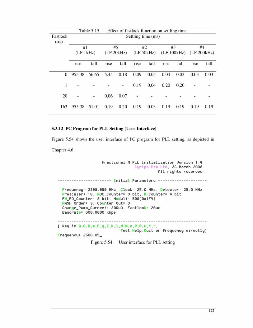
122
Table 5.15 Effect of fastlock function on settling time
Settling time (ms)
#1 (LF 1kHz)
#5 (LF 20kHz)
#2 (LF 50kHz)
#3 (LF 100kHz)
#4 (LF 200kHz)
Fastlock
(µs)
rise fall rise fall rise fall rise fall rise fall
0 955.38 56.65 5.45 0.18 0.09 0.05 0.04 0.03 0.03 0.03
1 - - - - 0.19 0.04 0.20 0.20 - -
20 - - 0.06 0.07 - - - - - -
163 955.38 51.01 0.19 0.20 0.19 0.03 0.19 0.19 0.19 0.19
5.3.12 PC Program for PLL Setting (User Interface)
Figure 5.54 shows the user interface of PC program for PLL setting, as depicted in
Chapter 4.6.
Figure 5.54 User interface for PLL setting

123
CHAPTER 6
CONCLUSION
A high frequency, robust, fast switching quad-modulus prescaler in a fully integrated,
versatile, low noise and fast-locking fractional-N frequency synthesizer has been
proposed and implemented with a 0.35µm CMOS technology.
The proposed frequency synthesizer consists of R-Counter, N-Counter, Fast-lock
Timer and Fast-lock Control Switch, MASH, Interface, Mode Register, MUX_Output,
PFD, Charge Pump and Quad-modulus Prescaler. Interface will receive external PLL
control commands and pass the data to respective blocks and R-Counter will divide
down the input reference frequency. The PFD serves as a phase- and frequency-
difference evaluator between divided reference frequency and divided LO frequency,
and outputs UP/DN pulses. Then, the outputs are fed to Charge Pump which offers 6
different current settings. Fast-lock function is integrated to shorten the frequency
locking time. The advantages of Charge Pump PLL are: the capture range is only
restricted by VCO output frequency range, and no static phase error if mismatches and
offsets are negligible. The dead-zone in PFD has been eliminated by implementation
of delay cells. The Charge Pump current will pass through loop filter, and the DC
voltage is used to control the VCO. The Loop filter is connected externally to
eliminate the issues of process sensitivity, temperature variations and aging. Then, the
VCO output frequency will be divided down by Prescaler, which offers 4 division
ratios.

124
Prescaler block faced the most challenge in this synthesizer design because the
0.35µm CMOS technology used for this design had a Transit frequency (fT) of less
than 50GHz, which restrained the maximum achievable operating frequency for multi-
modulus divider. Hence, much work was needed in optimizing and compromising
between the maximum operating frequency, power consumption, die size, and other
properties. In the proposed quad-modulus prescaler design, CML topology was
implemented in the construction of dividers to optimize the circuit’s maximum
operating frequency and minimize the switching noise contributed by hard-switching
of MOSFETs in other topologies. Besides, analog logic gates and gate-embedded
latches were used to meet the high-speed, high-frequency operation requirement. The
total dynamic power consumption was controlled by allowing only three synchronous
divider operating at highest frequency, with each having current biasing to control the
total current consumption during switching. The subsequent asynchronous dividers
had been optimized to minimize the overall power consumption since they are
operating at a lower frequency. The overall architecture of the prescaler was designed
in such a way that it can be easily deployed for other division ratio with minimal
amendments required.
A MASH which offers 3rd
and 4th
order selection was designed to produce fractional
output frequency. The generated pseudo-random number is added to the N-Counter
register value, and set as the initial value for N-Counter. N-Counter will then divide
down the Prescaler output frequency before feeding the signal to MASH and PFD, and
generate modulus-selection signals for Prescaler. Mode Register will set the MASH
order, frequency synthesizer output and charge pump current, and MUX_Output will

125
select signal from R-Counter output, prescaler output, divider output or lock detector
output to be transmitted out for testing purpose.
The proposed design had been analyzed, implemented and simulated at both circuit
and system levels. The actual performances of the circuit were further verified via
testing and measurements which were carried out after fabrication and packaging. The
chip area of the design was 853.65µm * 819.05µm. Table 6.1 summarizes the
measured performances of the fractional-N frequency synthesizer. Unless otherwise
stated, the measurements were carried out in the following conditions: Vdd= 3.3V,
Temp.= 250C, loop bandwidth= 20kHz (2nd order), MASH order= 3, operating
frequency= 2450MHz.
Table 6.1 Summary table for fractional-N frequency synthesizer performance
Value Parameter
Min Typ Max
Unit
Crystal oscillating frequency 25.0026 25.0029 25.0032 MHz
Operating frequency 2076.95 2574.50 MHz
Reference spurs
@ 25MHz offset -71.38 dBc
Fractional spurs @ 2462.50MHz
@ 25MHz offset -60.61 dBc
@ 50MHz offset -61.26 dBc
@ 75MHz offset -64.00 dBc
Integer-N boundary spurs - refer to Figure 5.47 and Figure 5.48 -
Phase noise
@ 10kHz offset -65.84 dBc/Hz
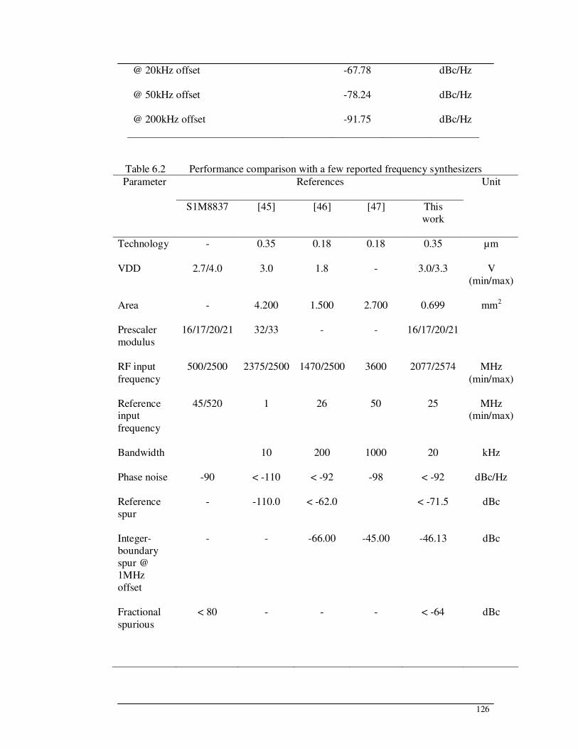
126
@ 20kHz offset -67.78 dBc/Hz
@ 50kHz offset -78.24 dBc/Hz
@ 200kHz offset -91.75 dBc/Hz
Table 6.2 Performance comparison with a few reported frequency synthesizers
References Parameter
S1M8837 [45] [46] [47] This
work
Unit
Technology - 0.35 0.18 0.18 0.35 µm
VDD 2.7/4.0 3.0 1.8 - 3.0/3.3 V
(min/max)
Area - 4.200 1.500 2.700 0.699 mm2
Prescaler
modulus
16/17/20/21 32/33 - - 16/17/20/21
RF input
frequency
500/2500 2375/2500 1470/2500 3600 2077/2574 MHz
(min/max)
Reference input
frequency
45/520 1 26 50 25 MHz (min/max)
Bandwidth 10 200 1000 20 kHz
Phase noise -90 < -110 < -92 -98 < -92 dBc/Hz
Reference
spur
- -110.0 < -62.0 < -71.5 dBc
Integer-
boundary
spur @
1MHz
offset
- - -66.00 -45.00 -46.13 dBc
Fractional
spurious
< 80 - - - < -64 dBc
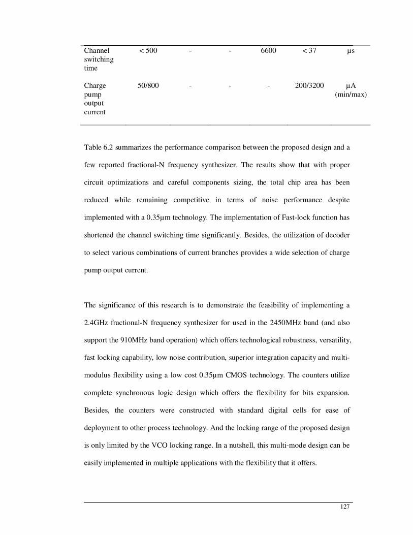
127
Channel
switching
time
< 500 - - 6600 < 37 µs
Charge
pump output
current
50/800 - - - 200/3200 µA
(min/max)
Table 6.2 summarizes the performance comparison between the proposed design and a
few reported fractional-N frequency synthesizer. The results show that with proper
circuit optimizations and careful components sizing, the total chip area has been
reduced while remaining competitive in terms of noise performance despite
implemented with a 0.35µm technology. The implementation of Fast-lock function has
shortened the channel switching time significantly. Besides, the utilization of decoder
to select various combinations of current branches provides a wide selection of charge
pump output current.
The significance of this research is to demonstrate the feasibility of implementing a
2.4GHz fractional-N frequency synthesizer for used in the 2450MHz band (and also
support the 910MHz band operation) which offers technological robustness, versatility,
fast locking capability, low noise contribution, superior integration capacity and multi-
modulus flexibility using a low cost 0.35µm CMOS technology. The counters utilize
complete synchronous logic design which offers the flexibility for bits expansion.
Besides, the counters were constructed with standard digital cells for ease of
deployment to other process technology. And the locking range of the proposed design
is only limited by the VCO locking range. In a nutshell, this multi-mode design can be
easily implemented in multiple applications with the flexibility that it offers.

128
Future works which may be carried out include expanding the bit number of FN and
FD registers to 23 bits to reduce the spurious levels of various spurs, and
implementing a programmable digital loop filter.

129
BIBLIOGRAPHY
[1] Craninckx J. and Steyaert M.. A Fully Integrated CMOS DCS-1800 Frequency
Synthesizer, IEEE Journal of Solid-State Circuits, Vol. 33, No. 12. 1998.
[2] Mao, X., H. Yang and H. Wang. New Frequency Divider with 8 Output Phases
for Phase switching Prescaler. In Proc. of IEEE International Conference on
Communications, Circuits and Systems, June 2006, Vol. 4, pp. 2588-2591.
[3] Shu, K. and E. Sanchez-Sinencio. A 5-GHz Prescaler using Improved Phase
Switching. In Proc. of IEEE International Symposium on Circuits and Systems,
May 2002, Vol. 3, pp. 85-88.
[4] Craninckx, J. and M.S.J. Steyaert. A 1.75-GHz/3-V Dual-modulus Divide-by-
128/129 Prescaler in 0.7-µm CMOS, IEEE Journal of Solid-State Circuits, Vol.
31, No. 7, pp. 890-897. 1996.
[5] Saul, P.H. and M.S.J. Mudd. A Direct Digital Synthesizer with 100-MHz
Output Capability, IEEE Journal of Solid-State Circuits, Vol. 23, No. 3, pp.
819-821. 1998.
[6] Razavi, B.. Monolithic Phase-Locked Loops and Clock Recovery Circuits.
New York: IEEE Press. 1996.
[7] Bellaouar, A., M.S. O’brecht, A.M. Fahim and M.I. Elmasry. Low-Power
Direct Digital Frequency Synthesis for Wireless Communications, IEEE
Journal of Solid-State Circuits, Vol. 35, No. 3, pp. 385-390. 2000.
[8] Torosyan, A., D. Fu and A.N. Willson, Jr. A 300-MHz Quadrature Direct
Digital Synthesizer/Mixer in 0.25-µm CMOS, IEEE Journal of Solid-State
Circuits, Vol. 38, No. 6, pp. 875-887. 2003.
130
[9] Hsu, T.Y., B.J. Shieh and C.Y. Lee. An All-Digital Phase-Locked Loop
(ADPLL)-based Clock Recovery Circuit, IEEE Journal of Solid-State Circuits,
Vol. 34, No. 8, pp. 1063-1073. 1999.
[10] Ekroot, C.G. and S.I. Long. A GaAs 4-bit Adder-Accumulator Circuit for
Direct Digital Synthesis, IEEE Journal of Solid-State Circuits, Vol. 23, No. 2,
pp. 573-580. 1988.
[11] Yamagishi, A., M. Ishikawa, T. Tsukahara and S. Date. A 2-V, 2-GHz Low-
Power Direct Digital Frequency Synthesizer Chip-Set for Wireless
Communication, IEEE Journal of Solid-State Circuits, Vol. 33, No. 2, pp. 210-
217. 1998.
[12] Madisetti, A., A.Y. Kwentus and A.N. Willson, Jr. A 100-MHz, 16-b, Direct
Digital Frequency Synthesizer with a 100-dBc Spurious-Free Dynamic Range,
IEEE Journal of Solid-State Circuits, Vol. 34, No. 8, pp. 1034-1043. 1999.
[13] Park, B.H. and P.E. Allen. A 1GHz, Low-Phase-Noise CMOS Frequency
Synthesizer with Integrated LC VCO for Wireless Communications. In Proc.
of IEEE Custom Integrated Circuits Conference, May 1998, pp. 567-570.
[14] Riley, T.A.D., M.A. Copeland and T.A. Kwasniewski. Delta-Sigma
Modulation in Fractional-N Frequency Synthesis, IEEE Journal of Solid-State
Circuits, Vol. 28, No. 5, pp. 553-559. 1993.
[15] Rhee, W., B.S. Song and A. Ali. A 1.1-GHz CMOS Fractional-N Frequency
Synthesizer with a 3-b Third-Order ∆Σ Modulator, IEEE Journal of Solid-State
Circuits, Vol.35, No. 10, pp. 1453-1460. 2000.
[16] Filiol, N.M., T.A.D. Riley, C. Plett and M.A. Copeland. An Agile ISM Band
Frequency Synthesizer with Built-In GMSK Data Modulation, IEEE Journal of
Solid-State Circuits, Vol. 33, No. 7, pp. 998-1008. 1998.

131
[17] Perrott, M.H., T.L. Tewksbury and C.G. Sodini. A 27mW CMOS Fractional-N
Synthesizer/Modulator IC. In Proc. of 44th IEEE International Solid-State
Circuits Conference, February 1997, pp. 366-367.
[18] Myer, D.P. A Multicarrier Feedforward Amplifier Design, Microwave Journal,
pp. 78-88. 1994.
[19] Reddy, A.. Noise Shaping with Sigma Delta Modulators in Fractional-N
Synthesizers. In Proc. of IEEE International Workshop on Radio-Frequency
Integration Technology, December 2007, pp. 329-332.
[20] Chien, G. and P.R. Gray. A 900-MHz Local Oscillator using a DLL-based
Frequency Multiplier Technique for PCS Applications, IEEE Journal of Solid-
State Circuits, Vol. 35, No. 12, pp. 1996-1999. 2000.
[21] Kang, S.M. and Y. Leblebici. CMOS Digital Integrated Circuits: Analysis and
Design. 3rd Edition, McGraw-Hill Professional. 2002.
[22] Banerjee, D.. PLL Performance, Simulation and Design. 4th
Edition, Dog Ear
Publishing, LLC. 2006.
[23] Yu, X.P., M.A. Do, J.G. Ma and K.S. Yeo. A New 5GHz CMOS Dual-
Modulus Prescaler. In Proc. of IEEE International Symposium on Circuits and
Systems, May 2005, Vol. 5, pp. 5027-5030.
[24] Quan, Y., H. Yang, F. Dong and Y. Tao. “Time Borrowing” Technique for
Design of Low-Power High-Speed Multi-Modulus Prescaler in Frequency
Synthesizer. In Proc. of IEEE International Symposium on Circuits and
Systems, May 2008, pp. 1004-1007.
[25] Mo Y., E. Skafidas, R. Evans and I. Mareels. A 40GHz Power Efficient Static
CML Frequency Divider in 0.13-µm CMOS Technology for High Speed
Millimeter-Wave Wireless Systems. In Proc. of 4th
IEEE International

132
Conference on Circuits and Systems for Communications, May 2008, pp. 812-
815.
[26] Yamamoto, K. and M. Fujishima. 70GHz CMOS Harmonic Injection-Locked
Divider. In Proc. of IEEE International Solid-State Circuits Conference,
February 2006, pp. 2472-2481.
[27] Chen, W.Z. and C.L. Kuo. 18GHz and 7GHz Superharmonic Injection-Locked
Dividers in 0.25µm CMOS Technology. In Proc. of IEEE 28th
European Solid-
State Circuits Conference, September 2002, pp. 89-92.
[28] Razavi B., et. al.. Design of High Speed, Low Power Frequency Dividers and
Phase-Locked Loops in Deep Submicron CMOS, JSSC, February 1995, pp.
101-109.
[29] Wang H.M.. A 1.8V 3mW 16.8GHz Frequency Divider in 0.25µm CMOS,
ISSCC 2000, pp. 196-197.
[30] Shu, K., E. Sanchez-Sinencio, J. Silva-Martinez and S.H.K. Embabi. A 16mW,
2.23~2.45GHz Fully Integrated Σ∆ PLL with Novel Prescaler and Loop Filter
in 0.35µm CMOS. In IEEE Radio Frequency Integrated Circuits Symposium,
June 2003, pp. 181-184.
[31] Ahn, H.J. and M. Ismail. GHz Programmable Dual-Modulus Prescaler for
Multi-Standard Wireless Applications. In IEEE International Symposium on
Circuits and Systems, May 2002, Vol. 1, pp. I-137-I-140.
[32] Kamoto, T., N. Adachi and K. Yamashita. High-Speed Multi-Modulus
Prescaler IC. In Proc. of Fourth IEEE International Conference on Universal
Personal Communications, Nov 1995, pp. 325-328.

133
[33] Vaucher, C.S., I. Ferencic, M. Locher, et. al. A Family of Low-Power Truly
Modular Programmable Dividers in Standard 0.35-µm CMOS Technology,
IEEE Journal of Solid-State Circuits, Vol. 35, No. 7, pp. 1039-1045. 2000.
[34] Wafa, A. and A. Ahmed. High-Speed RF Multi-Modulus Prescaler
Architecture for Σ-∆ Fractional-N PLL Frequency Synthesizers. In Proc. of
IEEE International Symposium on Circuits and Systems, May 2004, Vol. 4, pp.
241-244.
[35] Krishnapura, N. and P.R. Kinget. A 5.3-GHz Programmable Divider for
HiperLAN in 0.25-µm CMOS, IEEE Journal of Solid-State Circuits, Vol. 35,
pp. 1019-1024. 2000.
[36] Shu, K., E. Sanchez-Sinencio, J. Silva-Martinez and S.H.K. Embabi. A 2.4GHz
Monolithic Fractional-N Frequency Synthesizer with Robust Phase-Switching
Prescaler and Loop Capacitance Multiplier, IEEE Journal of Solid-State
Circuits, Vol. 38, pp. 866-874. 2003
[37] Chen, W.Z., C.L. Kuo and C.C. Liu. 10GHz Quadrature-Phase Voltage
Controlled Oscillator and Prescaler. In Proc. of 29th
European Solid-State
Circuits Conference, Septemter 2003, pp. 361-364.
[38] de Miranda, F.P.H., Jr.S.J. Navarro and W.A.M. Van Noije. A 4GHz Dual
Modulus Divider-by 32/33 Prescaler in 0.35µm CMOS Technology. In Proc.
of 17th Symposium on Integrated Circuits and Systems Design, September
2004, pp. 94-99.
[39] Yang, C.Y., G.K. Dehng, J.M. Hsu and S.I. Liu. New Dynamic Flip-Flops for
High-Speed Dual-Modulus Prescaler, IEEE Journal of Solid-State Circuits, Vol.
33, No. 10, pp. 1568-1571. 1998.

134
[40] Wafa, A. and A. Ahmed. High-Speed RF Multi-Modulus Prescaler
Architecture for Σ-∆ Fractional-N PLL Frequency Synthesizers. In Proc. of
2004 International Symposium on Circuits and Systems, May 2004, Vol. 4, pp.
241-244.
[41] Soyuer, M. and R.G. Meyer. Frequency Limitation of a Conventional Phase-
Frequency Detector, IEEE Journal of Solid-State Circuits, Vol. 25, No. 4,
pp.1019-1022. 1990.
[42] Sharpe, C.A.. A 3-state Phase Detector Can Improved Your Next PLL Design,
EDN, pp. 55-59. 1976.
[43] Mizuno, M., M. Yamashina, K. Furuta, et. al.. A GHz MOS Adaptive Pipeline
Technique Using MOS Current-Mode Logic, IEEE Journal of Solid-State
Circuits, Vol. 31, No. 6, pp. 784-791. 1996.
[44] Romano, L., S. Levantino, S. Pellerano, et. al.. Low Jitter Design of a 0.35µm-
CMOS frequency divider operating up to 3GHz. In Proc. of 28th
European
Solid-State Circuits Conference, Sept 2002, pp. 611-614.
[45] Rana, R.S. and A.C. Patel. A Fast Settling, Low Phase Noise, Digitally
Controlled 2.4GHz CMOS 12-bit Σ∆ Fractional-N Synthesizer with
Programmable Step Sizes. In Proc. of 2003 IEEE Radio Frequency Integrated
Circuits Symposium, June 2003, pp. 285-287.
[46] Yu, X.Y., Y.F. Sun, W. Rhee, H.K. Ahn, B.H. Park and Z.H. Wang. A ∆Σ
Fractional-N Synthesizer with Customized Noise Shaping for
WCDMA/HSDPA Applications, IEEE Journal of Solid-State Circuits, Vol. 44,
No. 8, pp. 2193-2201. 2009.
[47] Meninger, S.E. and M.H. Perrott. A 1-MHz Bandwidth 3.6-GHz 0.18-µm
CMOS Fractional-N Synthesizer Utilizing A Hybrid PFD/DAC Structure for

135
Reduced Broadband and Phase Noise, IEEE Journal of Solid-State Circuits,
Vol. 41, No. 4, pp. 966-980. 2006.

136
APPENDICES
Appendix A Reference Spur Plots
Unless otherwise stated, the settings for the measurements are as follow:
• RBW= 10kHz; VBW= 3kHz; Span= 60MHz; Sweep= 6s
• MASH= 3
• Moduli= 500
Figure A.1 #1 reference spur plot at
~25MHz offset (right)
Figure A.2 #1 reference spur plot at
10.80MHz offset (left)
Figure A.3 #1 reference spur plot at
~25MHz offset (left)
Figure A.4 #2 reference spur plot at
~25MHz offset (right)

137
Figure A.5 #2 reference spur plot at
10.80MHz offset (left)
Figure A.6 #2 reference spur plot at
~25MHz offset (left)
Figure A.7 #3 reference spur plot at
~25MHz offset (right)
Figure A.8 #3 reference spur plot at
10.80MHz offset (left)
Figure A.9 #3 reference spur plot at
~25MHz offset (left)
Figure A.10 #4 reference spur plot at
~25MHz offset (right)

138
Figure A.11 #4 reference spur at
10.80MHz offset (left)
Figure A.12 #4 reference spur at
~25MHz offset (left)
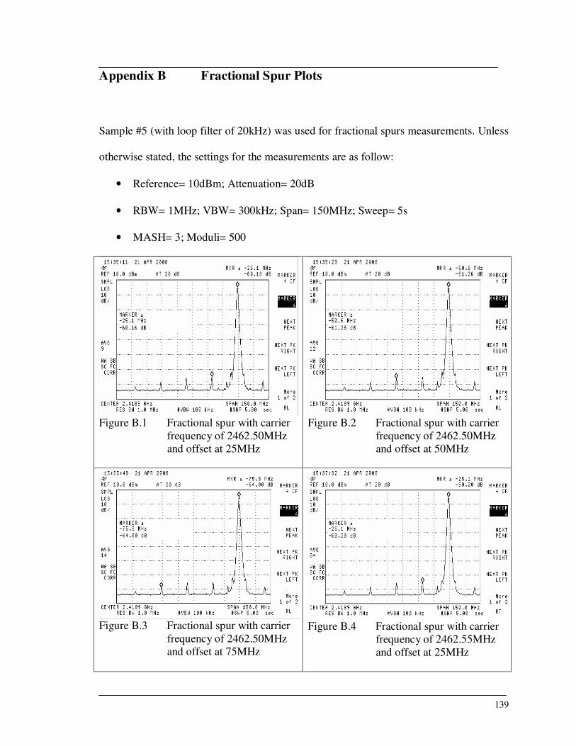
139
Appendix B Fractional Spur Plots
Sample #5 (with loop filter of 20kHz) was used for fractional spurs measurements. Unless
otherwise stated, the settings for the measurements are as follow:
• Reference= 10dBm; Attenuation= 20dB
• RBW= 1MHz; VBW= 300kHz; Span= 150MHz; Sweep= 5s
• MASH= 3; Moduli= 500
Figure B.1 Fractional spur with carrier
frequency of 2462.50MHz
and offset at 25MHz
Figure B.2 Fractional spur with carrier
frequency of 2462.50MHz
and offset at 50MHz
Figure B.3 Fractional spur with carrier
frequency of 2462.50MHz
and offset at 75MHz
Figure B.4 Fractional spur with carrier
frequency of 2462.55MHz
and offset at 25MHz

140
Figure B.5 Fractional spur with carrier
frequency of 2462.55MHz
and offset at 50MHz
Figure B.6 Fractional spur with carrier
frequency of 2462.55MHz
and offset at 75MHz
Figure B.7 Fractional spur with carrier
frequency of 2462.60MHz
and offset at 25MHz
Figure B.8 Fractional spur with carrier
frequency of 2462.60MHz
and offset at 50MHz
Figure B.9 Fractional spur with carrier
frequency of 2462.60MHz
and offset at 75MHz
Figure B.10 Fractional spur with carrier
frequency of 2462.65MHz
and offset at 25MHz
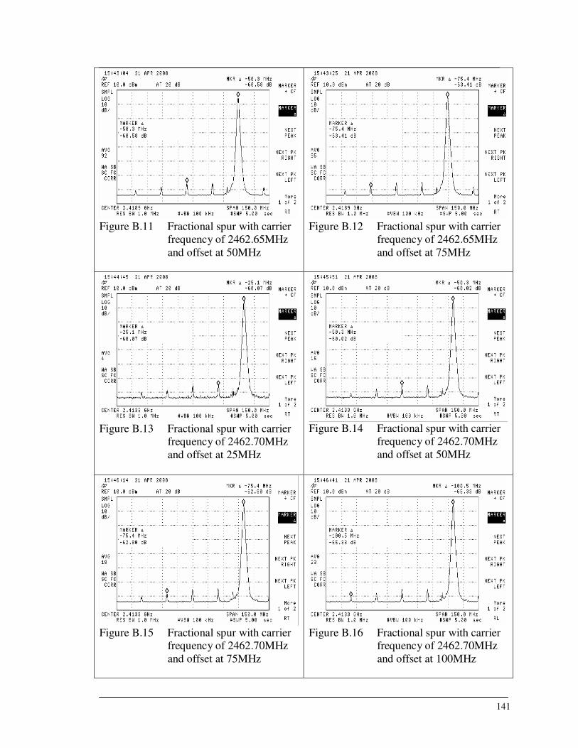
141
Figure B.11 Fractional spur with carrier
frequency of 2462.65MHz
and offset at 50MHz
Figure B.12 Fractional spur with carrier
frequency of 2462.65MHz
and offset at 75MHz
Figure B.13 Fractional spur with carrier
frequency of 2462.70MHz
and offset at 25MHz
Figure B.14 Fractional spur with carrier
frequency of 2462.70MHz
and offset at 50MHz
Figure B.15 Fractional spur with carrier
frequency of 2462.70MHz
and offset at 75MHz
Figure B.16 Fractional spur with carrier
frequency of 2462.70MHz
and offset at 100MHz

142
Figure B.17 Fractional spur with carrier
frequency of 2462.75MHz
and offset at 25MHz
Figure B.18 Fractional spur with carrier
frequency of 2462.75MHz
and offset at 50MHz
Figure B.19 Fractional spur with carrier
frequency of 2462.75MHz
and offset at 75MHz
Figure B.20 Fractional spur with carrier
frequency of 2462.75MHz
and offset at 100MHz
Figure B.21 Fractional spur with carrier
frequency of 2462.80MHz
and offset at 25MHz
Figure B.22 Fractional spur with carrier
frequency of 2462.80MHz
and offset at 50MHz

143
Figure B.23 Fractional spur with carrier
frequency of 2462.80MHz
and offset at 75MHz
Figure B.24 Fractional spur with carrier
frequency of 2462.80MHz
and offset at 100MHz
Figure B.25 Fractional spur with carrier
frequency of 2462.85MHz
and offset at 25MHz
Figure B.26 Fractional spur with carrier
frequency of 2462.85MHz
and offset at 50MHz
Figure B.27 Fractional spur with carrier
frequency of 2462.85MHz
and offset at 75MHz
Figure B.28 Fractional spur with carrier
frequency of 2462.85MHz
and offset at 100MHz

144
Figure B.29 Fractional spur with carrier
frequency of 2462.90MHz
and offset at 25MHz
Figure B.30 Fractional spur with carrier
frequency of 2462.90MHz
and offset at 50MHz
Figure B.31 Fractional spur with carrier
frequency of 2462.90MHz
and offset at 75MHz
Figure B.32 Fractional spur with carrier
frequency of 2462.90MHz
and offset at 100MHz
Figure B.33 Fractional spur with carrier
frequency of 2462.95MHz
and offset at 25MHz
Figure B.34 Fractional spur with carrier
frequency of 2462.95MHz
and offset at 50MHz
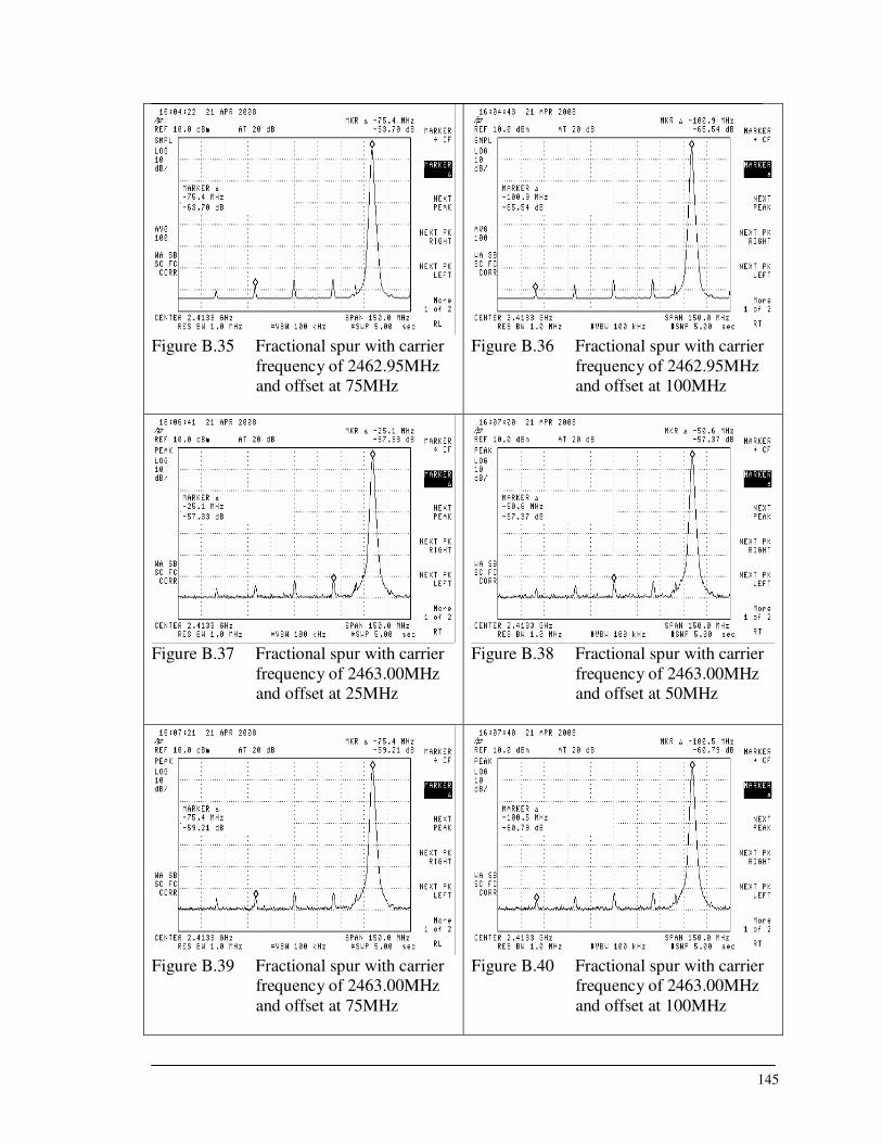
145
Figure B.35 Fractional spur with carrier
frequency of 2462.95MHz
and offset at 75MHz
Figure B.36 Fractional spur with carrier
frequency of 2462.95MHz
and offset at 100MHz
Figure B.37 Fractional spur with carrier
frequency of 2463.00MHz
and offset at 25MHz
Figure B.38 Fractional spur with carrier
frequency of 2463.00MHz
and offset at 50MHz
Figure B.39 Fractional spur with carrier
frequency of 2463.00MHz
and offset at 75MHz
Figure B.40 Fractional spur with carrier
frequency of 2463.00MHz
and offset at 100MHz

146
Figure B.41 Fractional spur with carrier
frequency of 2463.05MHz
and offset at 25MHz
Figure B.42 Fractional spur with carrier
frequency of 2463.05MHz
and offset at 50MHz
Figure B.43 Fractional spur with carrier
frequency of 2463.05MHz
and offset at 75MHz
Figure B.44 Fractional spur with carrier
frequency of 2463.05MHz
and offset at 100MHz
Figure B.45 Fractional spur with carrier
frequency of 2463.10MHz
and offset at 25MHz
Figure B.46 Fractional spur with carrier
frequency of 2463.10MHz
and offset at 50MHz
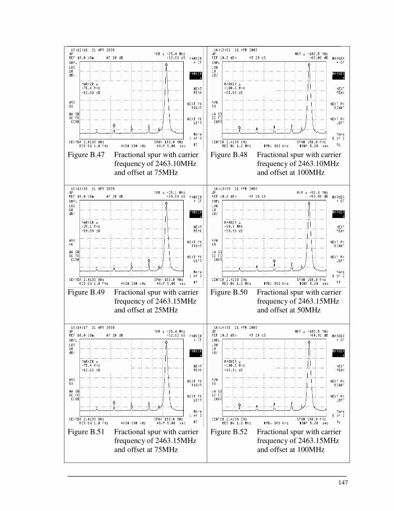
147
Figure B.47 Fractional spur with carrier
frequency of 2463.10MHz
and offset at 75MHz
Figure B.48 Fractional spur with carrier
frequency of 2463.10MHz
and offset at 100MHz
Figure B.49 Fractional spur with carrier
frequency of 2463.15MHz
and offset at 25MHz
Figure B.50 Fractional spur with carrier
frequency of 2463.15MHz
and offset at 50MHz
Figure B.51 Fractional spur with carrier
frequency of 2463.15MHz
and offset at 75MHz
Figure B.52 Fractional spur with carrier
frequency of 2463.15MHz
and offset at 100MHz

148
Figure B.53 Fractional spur with carrier
frequency of 2463.20MHz
and offset at 25MHz
Figure B.54 Fractional spur with carrier
frequency of 2463.20MHz
and offset at 50MHz
Figure B.55 Fractional spur with carrier
frequency of 2463.20MHz
and offset at 75MHz
Figure B.56 Fractional spur with carrier
frequency of 2463.20MHz
and offset at 100MHz
Figure B.57 Fractional spur with carrier
frequency of 2463.25MHz
and offset at 25MHz
Figure B.58 Fractional spur with carrier
frequency of 2463.25MHz
and offset at 50MHz

149
Figure B.59 Fractional spur with carrier
frequency of 2463.25MHz
and offset at 75MHz
Figure B.60 Fractional spur with carrier
frequency of 2463.25MHz
and offset at 100MHz
Figure B.61 Fractional spur with carrier
frequency of 2463.30MHz
and offset at 25MHz
Figure B.62 Fractional spur with carrier
frequency of 2463.30MHz
and offset at 50MHz
Figure B.63 Fractional spur with carrier
frequency of 2463.30MHz
and offset at 75MHz
Figure B.64 Fractional spur with carrier
frequency of 2463.30MHz
and offset at 100MHz

150
Appendix C Integer-N Boundary Spurs
Sample #5 (with loop filter of 20kHz) was used for integer-N boundary spurs
measurements. Unless otherwise stated, the settings for the measurements are as follow:
i) at carrier frequency= 2450.05MHz~2451.50MHz
• P2450M= 4.99dBm
• Reference= 10dBm; Attenuation= 20dB
• RBW= 10kHz; VBW= 100Hz; Span= 1MHz; Sweep= 3s
• MASH=3; Moduli= 500; FN= 20
ii) at carrier frequency= 2451.35MHz~2451.85MHz
• P2450M= 4.99dBm
• Reference= 10dBm; Attenuation= 20dB
• RBW= 10kHz; VBW= 100Hz; Span= 3MHz; Sweep= 1s
• MASH= 3; Moduli= 500; FN= 20
Table C.1 Integer-N boundary spurious levels at 2450MHz
Carrier frequency
(MHz)
Spurious level
at 2450MHz
(dBc)
Carrier frequency
(MHz)
Spurious level
at 2450MHz
(dBc)
2450.00 +4.99 2450.95 -53.44
2450.05 -25.22 2451.00 -46.13
2450.10 -28.97 2451.05 -55.26
2450.15 -32.50 2451.10 -55.35
2450.20 -32.10 2451.15 -53.52
2450.25 -35.17 2451.20 -51.84

151
Carrier frequency
(MHz)
Spurious level
at 2450MHz
(dBc)
Carrier frequency
(MHz)
Spurious level
at 2450MHz
(dBc)
2450.30 -38.41 2451.25 -50.13
2450.35 -39.69 2451.30 -59.32
2450.40 -40.28 2451.35 -60.59
2450.45 -42.24 2451.40 -53.37
2450.50 -45.53 2451.45 -60.21
2450.55 -47.01 2451.50 -58.87
2450.60 -47.57 2451.55 -60.49
2450.65 -49.61 2451.60 -56.23
2450.70 -48.83 2451.65 -60.73
2450.75 -47.98 2451.70 -63.30
2450.80 -46.27 2451.75 -59.23
2450.85 -51.37 2451.80 -63.01
2450.90 -52.42 2451.85 -63.98
Figure C.1 Integer-N boundary spur
with carrier frequency of
2450.00MHz
Figure C.2 Integer-N boundary spur
with carrier frequency of
2450.05MHz and offset at
50kHz

152
Figure C.3 Integer-N boundary spur
with carrier frequency of
2450.10MHz and offset at
100kHz
Figure C.4 Integer-N boundary spur
with carrier frequency of
2450.15MHz and offset at
150kHz
Figure C.5 Integer-N boundary spur
with carrier frequency of
2450.20MHz and offset at
200kHz
Figure C.6 Integer-N boundary spur
with carrier frequency of
2450.25MHz and offset at
250kHz
Figure C.7 Integer-N boundary spur
with carrier frequency of
2450.30MHz and offset at
300kHz
Figure C.8 Integer-N boundary spur
with carrier frequency of
2450.35MHz and offset at
350kHz
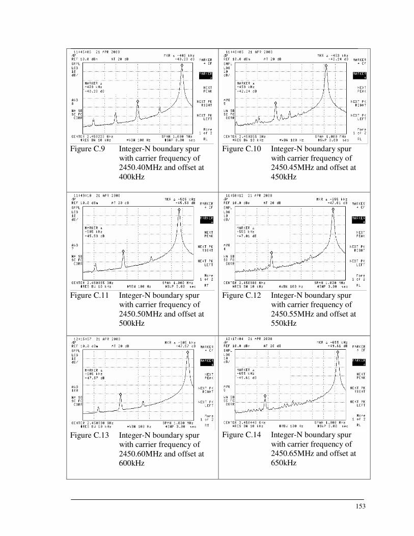
153
Figure C.9 Integer-N boundary spur
with carrier frequency of
2450.40MHz and offset at
400kHz
Figure C.10 Integer-N boundary spur
with carrier frequency of
2450.45MHz and offset at
450kHz
Figure C.11 Integer-N boundary spur
with carrier frequency of
2450.50MHz and offset at
500kHz
Figure C.12 Integer-N boundary spur
with carrier frequency of
2450.55MHz and offset at
550kHz
Figure C.13 Integer-N boundary spur
with carrier frequency of
2450.60MHz and offset at
600kHz
Figure C.14 Integer-N boundary spur
with carrier frequency of
2450.65MHz and offset at
650kHz

154
Figure C.15 Integer-N boundary spur
with carrier frequency of
2450.70MHz and offset at
700kHz
Figure C.16 Integer-N boundary spur
with carrier frequency of
2450.75MHz and offset at
750kHz
Figure C.17 Integer-N boundary spur
with carrier frequency of
2450.80MHz and offset at
800kHz
Figure C.18 Integer-N boundary spur
with carrier frequency of
2450.85MHz and offset at
850kHz
Figure C.19 Integer-N boundary spur
with carrier frequency of
2450.90MHz and offset at
900kHz
Figure C.20 Integer-N boundary spur
with carrier frequency of
2450.95MHz and offset at
950kHz

155
Figure C.21 Integer-N boundary spur
with carrier frequency of
2451.00MHz and offset at
1.00MHz
Figure C.22 Integer-N boundary spur
with carrier frequency of
2451.05MHz and offset at
1.05MHz
Figure C.23 Integer-N boundary spur
with carrier frequency of
2451.10MHz and offset at
1.10MHz
Figure C.24 Integer-N boundary spur
with carrier frequency of
2451.15MHz and offset at
1.15MHz
Figure C.25 Integer-N boundary spur
with carrier frequency of
2451.20MHz and offset at
1.20MHz
Figure C.26 Integer-N boundary spur
with carrier frequency of
2451.25MHz and offset at
1.25MHz

156
Figure C.27 Integer-N boundary spur
with carrier frequency of
2451.30MHz and offset at
1.30MHz
Figure C.28 Integer-N boundary spur
with carrier frequency of
2451.35MHz and offset at
1.35MHz
Figure C.29 Integer-N boundary spur
with carrier frequency of
2451.40MHz and offset at
1.40MHz
Figure C.30 Integer-N boundary spur
with carrier frequency of
2451.45MHz and offset at
1.45MHz
Figure C.31 Integer-N boundary spur
with carrier frequency of
2451.50MHz and offset at
1.50MHz
Figure C.32 Integer-N boundary spur
with carrier frequency of
2451.55MHz and offset at
1.55MHz

157
Figure C.33 Integer-N boundary spur
with carrier frequency of
2451.60MHz and offset at
1.60MHz
Figure C.34 Integer-N boundary spur
with carrier frequency of
2451.65MHz and offset at
1.65MHz
Figure C.35 Integer-N boundary spur
with carrier frequency of
2451.70MHz and offset at
1.70MHz
Figure C.36 Integer-N boundary spur
with carrier frequency of
2451.75MHz and offset at
1.75MHz
Figure C.37 Integer-N boundary spur
with carrier frequency of
2451.80MHz and offset at
1.80MHz
Figure C.38 Integer-N boundary spur
with carrier frequency of
2451.85MHz and offset at
1.85MHz
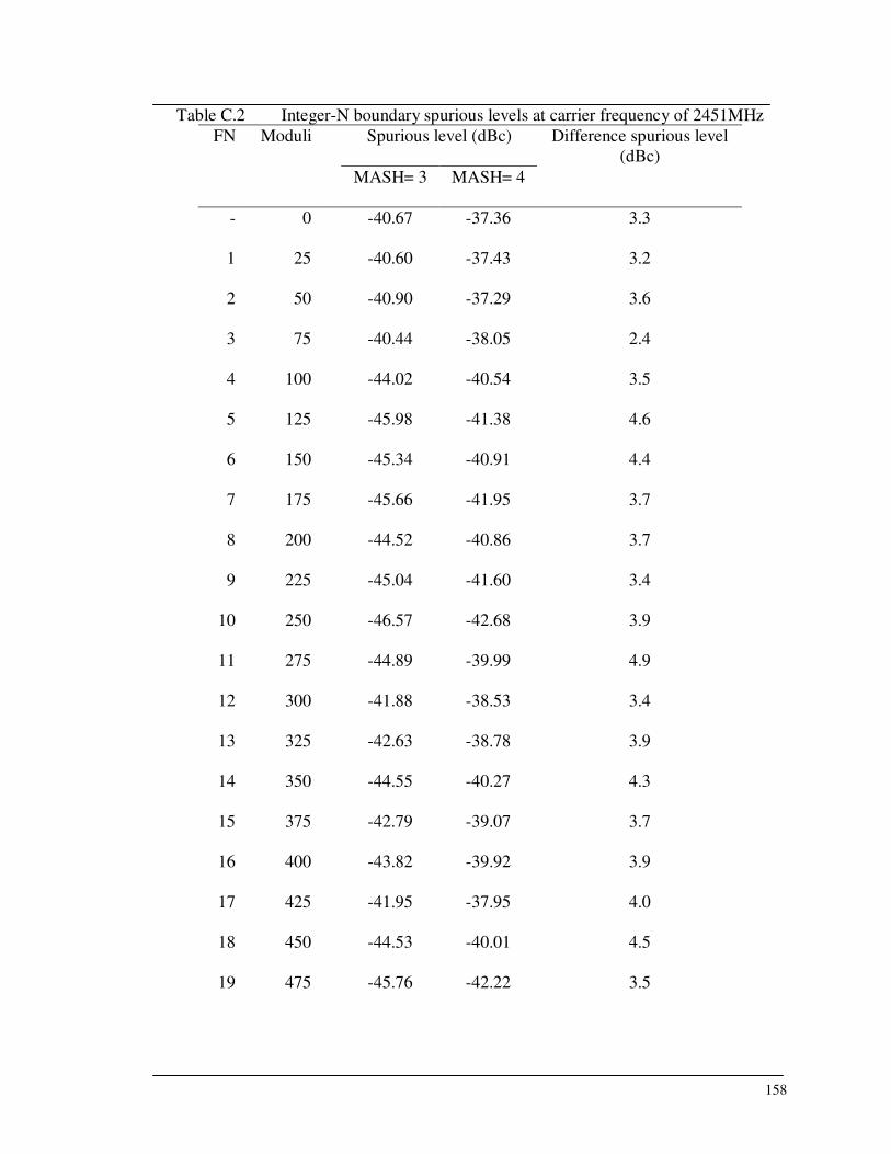
158
Table C.2 Integer-N boundary spurious levels at carrier frequency of 2451MHz
Spurious level (dBc) FN Moduli
MASH= 3 MASH= 4
Difference spurious level
(dBc)
- 0 -40.67 -37.36 3.3
1 25 -40.60 -37.43 3.2
2 50 -40.90 -37.29 3.6
3 75 -40.44 -38.05 2.4
4 100 -44.02 -40.54 3.5
5 125 -45.98 -41.38 4.6
6 150 -45.34 -40.91 4.4
7 175 -45.66 -41.95 3.7
8 200 -44.52 -40.86 3.7
9 225 -45.04 -41.60 3.4
10 250 -46.57 -42.68 3.9
11 275 -44.89 -39.99 4.9
12 300 -41.88 -38.53 3.4
13 325 -42.63 -38.78 3.9
14 350 -44.55 -40.27 4.3
15 375 -42.79 -39.07 3.7
16 400 -43.82 -39.92 3.9
17 425 -41.95 -37.95 4.0
18 450 -44.53 -40.01 4.5
19 475 -45.76 -42.22 3.5

159
Spurious level (dBc) FN Moduli
MASH= 3 MASH= 4
Difference spurious level
(dBc)
20 500 -45.11 -41.19 3.9
Max -40.44 -37.29 4.9
Min -46.57 -42.68 2.4
Delta 6.13 5.39 2.5
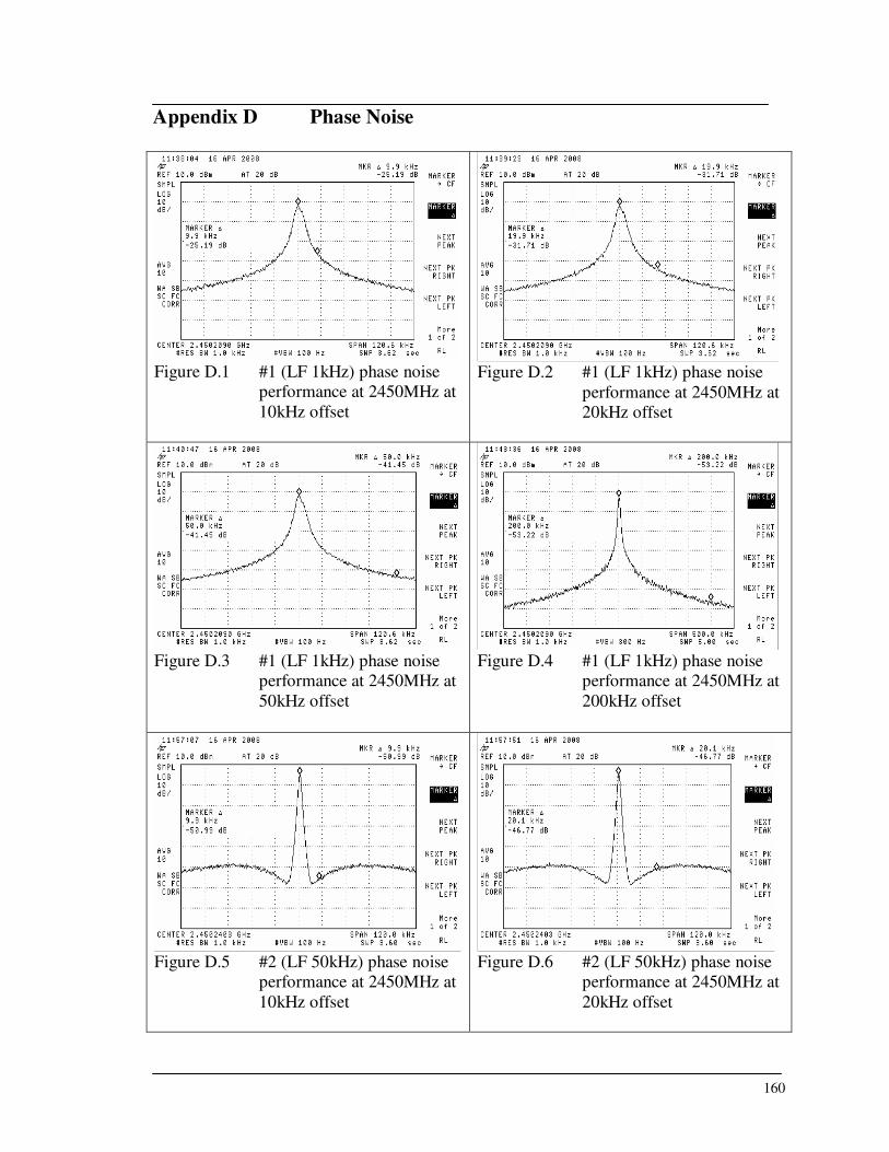
160
Appendix D Phase Noise
Figure D.1 #1 (LF 1kHz) phase noise
performance at 2450MHz at
10kHz offset
Figure D.2 #1 (LF 1kHz) phase noise
performance at 2450MHz at
20kHz offset
Figure D.3 #1 (LF 1kHz) phase noise
performance at 2450MHz at
50kHz offset
Figure D.4 #1 (LF 1kHz) phase noise
performance at 2450MHz at
200kHz offset
Figure D.5 #2 (LF 50kHz) phase noise
performance at 2450MHz at
10kHz offset
Figure D.6 #2 (LF 50kHz) phase noise
performance at 2450MHz at
20kHz offset

161
Figure D.7 #2 (LF 50kHz) phase noise
performance at 2450MHz at
50kHz offset
Figure D.8 #2 (LF 50kHz) phase noise
performance at 2450MHz at
200kHz offset
Figure D.9 #3 (LF 100kHz) phase noise
performance at 2450MHz at
10kHz offset
Figure D.10 #3 (LF 100kHz) phase noise
performance at 2450MHz at
20kHz offset
Figure D.11 #3 (LF 100kHz) phase noise
performance at 2450MHz at
50kHz offset
Figure D.12 #3 (LF 100kHz) phase noise
performance at 2450MHz at
200kHz offset

162
Figure D.13 #4 (LF 200kHz) phase noise
performance at 2450MHz at
10kHz offset
Figure D.14 #4 (LF 200kHz) phase noise
performance at 2450MHz at
20kHz offset
Figure D.15 #4 (LF 200kHz) phase noise
performance at 2450MHz at
50kHz offset
Figure D.16 #4 (LF 200kHz) phase noise
performance at 2450MHz at
200kHz offset
Figure D.17 #5 (LF 20kHz) phase noise
performance at 2450MHz at
10kHz offset
Figure D.18 #5 (LF 20kHz) phase noise
performance at 2450MHz at
20kHz offset

163
Figure D.19 #5 (LF 20kHz) phase noise
performance at 2450MHz at
50kHz offset
Figure D.20 #5 (LF 20kHz) phase noise
performance at 2450MHz at
200kHz offset