Embed Size (px)
Citation preview
June 2006Jukka Tapio Typpø, IETOddgeir Fikstvedt, Micrel
Master of Science in ElectronicsSubmission date:Supervisor:Co-supervisor:
Norwegian University of Science and TechnologyDepartment of Electronics and Telecommunications
Design of a 5.8 GHz Multi-ModulusPrescaler
Vidar Myklebust

Problem DescriptionEn prescaler er en viktig byggeblokk i en PLL der den deler ned VCO frekvensen til en laverefrekvens før fasedetektoren. En 5.8GHz multi-modulus prescaler skal designes i en 0.18ummixedsignalCMOS prosess. Denne skal brukes i en ISM-bånd transceiver.
Studenten skal basert på litteraturstudie finne arkitekturer som er egnet for on-chipimplementasjon i CMOS. Utfra disse aktuelle arkitekturene skal hun/han finne den beste medtanke på strømforbruk og areal.Den valgte arkitekturen skal implementeres 0.18um CMOS.
Frekvens: 5.8GHzModulu: 64Strømforbruk: 4mA
Assignment given: 16. January 2006Supervisor: Jukka Tapio Typpø, IET

Abstract
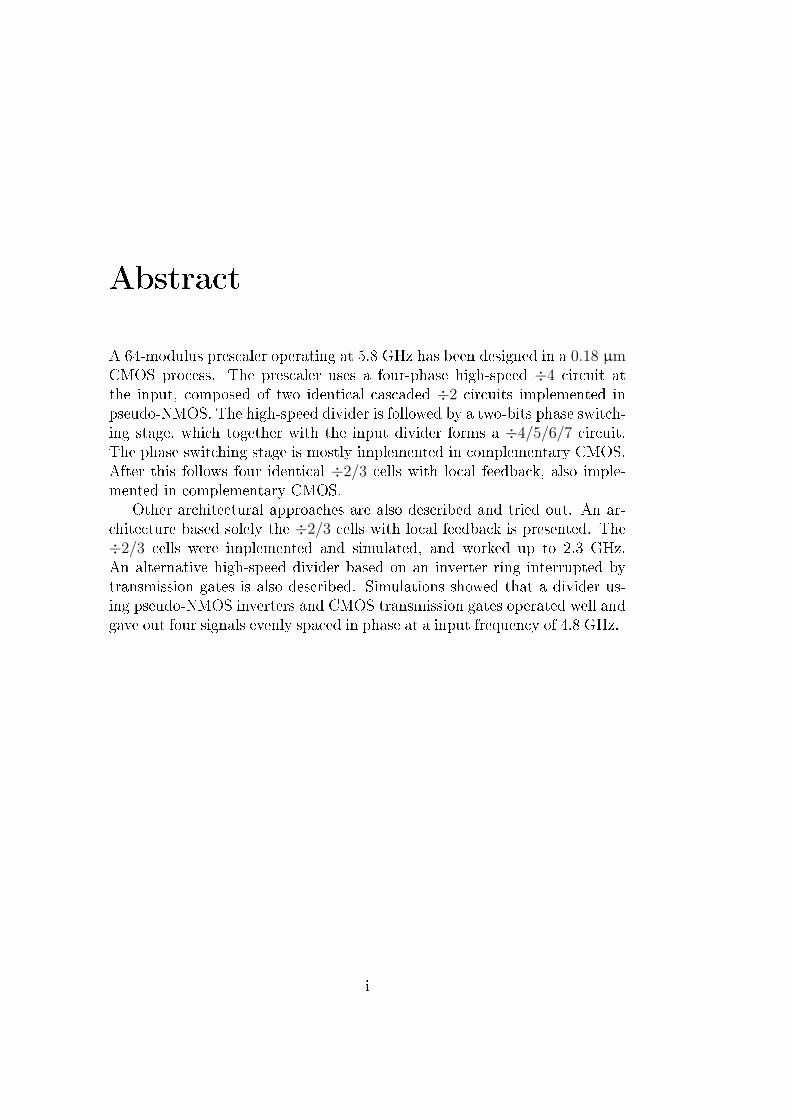
A 64-modulus prescaler operating at 5.8 GHz has been designed in a 0.18 µmCMOS process. The prescaler uses a four-phase high-speed ÷4 circuit atthe input, composed of two identical cascaded ÷2 circuits implemented inpseudo-NMOS. The high-speed divider is followed by a two-bits phase switch-ing stage, which together with the input divider forms a ÷4/5/6/7 circuit.The phase switching stage is mostly implemented in complementary CMOS.After this follows four identical ÷2/3 cells with local feedback, also imple-mented in complementary CMOS.
Other architectural approaches are also described and tried out. An ar-chitecture based solely the ÷2/3 cells with local feedback is presented. The÷2/3 cells were implemented and simulated, and worked up to 2.3 GHz.An alternative high-speed divider based on an inverter ring interrupted bytransmission gates is also described. Simulations showed that a divider us-ing pseudo-NMOS inverters and CMOS transmission gates operated well andgave out four signals evenly spaced in phase at a input frequency of 4.8 GHz.
i

ii
Preface
This report has been written for Micrel as part of my master thesis at Depart-ment of Electronics and Telecommunications at the Norwegian University ofScience and Technology (NTNU).
The work with this thesis has lasted for 20 weeks, and was �nished inJune 2006. At times the work has been hard and frustrating, but I feel thatI have also learned a lot.
My technical teacher at NTNU has been Jukka Typpö, and my teachingsupervisor at Micrel has been Oddgeir Fikstvedt. Thanks to both of themfor valuable guidance during this period.
.
.
.
.Trondheim, June 2006..Vidar Myklebust
iii

iv
Contents
1 Introduction 1
2 Background Theory 3
2.1 Basic Circuits . . . . . . . . . . . . . . . . . . . . . . . . . . . 32.1.1 The Johnson Counter (÷2) . . . . . . . . . . . . . . . . 32.1.2 ÷3 Circuit . . . . . . . . . . . . . . . . . . . . . . . . . 42.1.3 Dual-Modulus ÷2/3 Circuit . . . . . . . . . . . . . . . 5
2.2 Multi-Modulus Circuits . . . . . . . . . . . . . . . . . . . . . . 62.3 Phase Switching . . . . . . . . . . . . . . . . . . . . . . . . . . 72.4 Pseudo-NMOS Logic . . . . . . . . . . . . . . . . . . . . . . . 8
3 ÷2/3 Cells With Local Feedback 11
3.1 ÷2/3 Cells Using Pseudo-NMOS Latches . . . . . . . . . . . . 113.2 ÷2/3 Cells Using CMOS Latches . . . . . . . . . . . . . . . . 12
4 High-Speed Inverter Ring Divider 15
5 Architecture Based on Phase-Switching 19
5.1 High-Speed Four-Phase ÷4 Circuit . . . . . . . . . . . . . . . 195.2 Four-Phase Phase Switcher . . . . . . . . . . . . . . . . . . . . 22
5.2.1 Four-to-One Multiplexer . . . . . . . . . . . . . . . . . 225.2.2 Phase Select State Machine . . . . . . . . . . . . . . . 235.2.3 Mapping Logic . . . . . . . . . . . . . . . . . . . . . . 25
5.3 ÷2/3 Stages . . . . . . . . . . . . . . . . . . . . . . . . . . . . 275.3.1 ÷2/3 Core . . . . . . . . . . . . . . . . . . . . . . . . . 275.3.2 Control Quali�er . . . . . . . . . . . . . . . . . . . . . 295.3.3 Mapping Logic . . . . . . . . . . . . . . . . . . . . . . 315.3.4 The Last ÷2/3 Stage . . . . . . . . . . . . . . . . . . . 32
5.4 Version 2 � ÷2/3 Cells With Local Feedback . . . . . . . . . . 335.5 Version 3 � Four-to-One Multiplexer Implemented in CMOS . 355.6 Version 4 � Alternative Local Feedback ÷2/3 Cell . . . . . . . 37
v
vi CONTENTS
6 Simulations 41
6.1 ÷2/3 Cells With Local Feedback . . . . . . . . . . . . . . . . 416.2 High-Speed Inverter Ring Divider . . . . . . . . . . . . . . . . 416.3 Architectures Based on Phase Switching . . . . . . . . . . . . 42
7 Results 45
7.1 ÷2/3 Cells With Local Feedback . . . . . . . . . . . . . . . . 457.2 High-Speed Inverter Ring Divider . . . . . . . . . . . . . . . . 467.3 Architectures Based on Phase Switching . . . . . . . . . . . . 46
8 Discussion 51
8.1 Choice of Architecture . . . . . . . . . . . . . . . . . . . . . . 518.1.1 High-Speed Input Divider . . . . . . . . . . . . . . . . 518.1.2 Phase Switching Stage . . . . . . . . . . . . . . . . . . 528.1.3 Low Frequency Stage . . . . . . . . . . . . . . . . . . . 52
8.2 Implementation . . . . . . . . . . . . . . . . . . . . . . . . . . 538.3 Simulations . . . . . . . . . . . . . . . . . . . . . . . . . . . . 53
9 Conclusion 55
A Simulation Plots 59
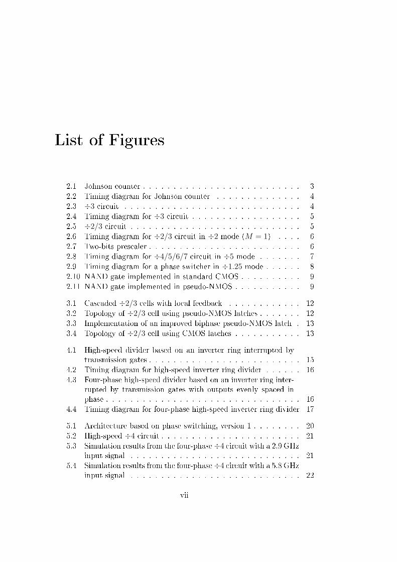
List of Figures
2.1 Johnson counter . . . . . . . . . . . . . . . . . . . . . . . . . . 3
2.2 Timing diagram for Johnson counter . . . . . . . . . . . . . . 4
2.3 ÷3 circuit . . . . . . . . . . . . . . . . . . . . . . . . . . . . . 4
2.4 Timing diagram for ÷3 circuit . . . . . . . . . . . . . . . . . . 5
2.5 ÷2/3 circuit . . . . . . . . . . . . . . . . . . . . . . . . . . . . 5
2.6 Timing diagram for ÷2/3 circuit in ÷2 mode (M = 1) . . . . 6
2.7 Two-bits prescaler . . . . . . . . . . . . . . . . . . . . . . . . . 6
2.8 Timing diagram for ÷4/5/6/7 circuit in ÷5 mode . . . . . . . 7
2.9 Timing diagram for a phase switcher in ÷1.25 mode . . . . . . 8
2.10 NAND gate implemented in standard CMOS . . . . . . . . . . 9
2.11 NAND gate implemented in pseudo-NMOS . . . . . . . . . . . 9
3.1 Cascaded ÷2/3 cells with local feedback . . . . . . . . . . . . 12
3.2 Topology of ÷2/3 cell using pseudo-NMOS latches . . . . . . . 12
3.3 Implementation of an improved biphase pseudo-NMOS latch . 13
3.4 Topology of ÷2/3 cell using CMOS latches . . . . . . . . . . . 13
4.1 High-speed divider based on an inverter ring interrupted bytransmission gates . . . . . . . . . . . . . . . . . . . . . . . . . 15
4.2 Timing diagram for high-speed inverter ring divider . . . . . . 16
4.3 Four-phase high-speed divider based on an inverter ring inter-rupted by transmission gates with outputs evenly spaced inphase . . . . . . . . . . . . . . . . . . . . . . . . . . . . . . . . 16
4.4 Timing diagram for four-phase high-speed inverter ring divider 17
5.1 Architecture based on phase switching, version 1 . . . . . . . . 20
5.2 High-speed ÷4 circuit . . . . . . . . . . . . . . . . . . . . . . . 21
5.3 Simulation results from the four-phase÷4 circuit with a 2.9 GHzinput signal . . . . . . . . . . . . . . . . . . . . . . . . . . . . 21
5.4 Simulation results from the four-phase÷4 circuit with a 5.8 GHzinput signal . . . . . . . . . . . . . . . . . . . . . . . . . . . . 22
vii
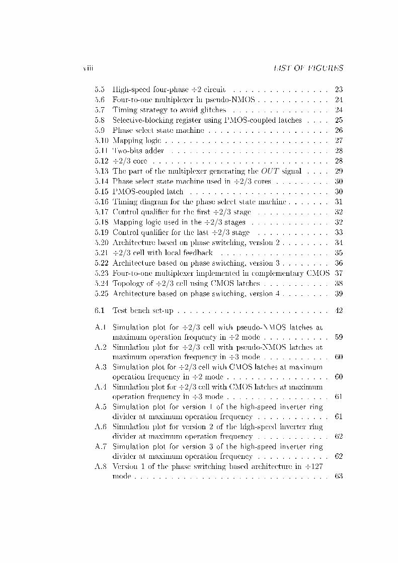
viii LIST OF FIGURES
5.5 High-speed four-phase ÷2 circuit . . . . . . . . . . . . . . . . 23
5.6 Four-to-one multiplexer in pseudo-NMOS . . . . . . . . . . . . 24
5.7 Timing strategy to avoid glitches . . . . . . . . . . . . . . . . 24
5.8 Selective-blocking register using PMOS-coupled latches . . . . 25
5.9 Phase select state machine . . . . . . . . . . . . . . . . . . . . 26
5.10 Mapping logic . . . . . . . . . . . . . . . . . . . . . . . . . . . 27
5.11 Two-bits adder . . . . . . . . . . . . . . . . . . . . . . . . . . 28
5.12 ÷2/3 core . . . . . . . . . . . . . . . . . . . . . . . . . . . . . 28
5.13 The part of the multiplexer generating the OUT signal . . . . 29
5.14 Phase select state machine used in ÷2/3 cores . . . . . . . . . 30
5.15 PMOS-coupled latch . . . . . . . . . . . . . . . . . . . . . . . 30
5.16 Timing diagram for the phase select state machine . . . . . . . 31
5.17 Control quali�er for the �rst ÷2/3 stage . . . . . . . . . . . . 32
5.18 Mapping logic used in the ÷2/3 stages . . . . . . . . . . . . . 32
5.19 Control quali�er for the last ÷2/3 stage . . . . . . . . . . . . 33
5.20 Architecture based on phase switching, version 2 . . . . . . . . 34
5.21 ÷2/3 cell with local feedback . . . . . . . . . . . . . . . . . . 35
5.22 Architecture based on phase switching, version 3 . . . . . . . . 36
5.23 Four-to-one multiplexer implemented in complementary CMOS 37
5.24 Topology of ÷2/3 cell using CMOS latches . . . . . . . . . . . 38
5.25 Architecture based on phase switching, version 4 . . . . . . . . 39
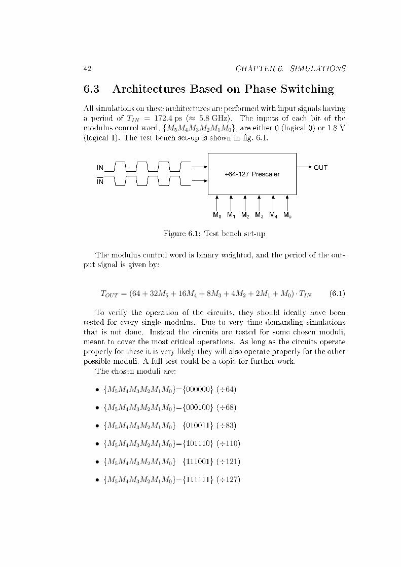
6.1 Test bench set-up . . . . . . . . . . . . . . . . . . . . . . . . . 42
A.1 Simulation plot for ÷2/3 cell with pseudo-NMOS latches atmaximum operation frequency in ÷2 mode . . . . . . . . . . . 59
A.2 Simulation plot for ÷2/3 cell with pseudo-NMOS latches atmaximum operation frequency in ÷3 mode . . . . . . . . . . . 60
A.3 Simulation plot for ÷2/3 cell with CMOS latches at maximumoperation frequency in ÷2 mode . . . . . . . . . . . . . . . . . 60
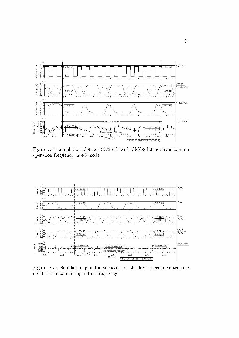
A.4 Simulation plot for ÷2/3 cell with CMOS latches at maximumoperation frequency in ÷3 mode . . . . . . . . . . . . . . . . . 61
A.5 Simulation plot for version 1 of the high-speed inverter ringdivider at maximum operation frequency . . . . . . . . . . . . 61
A.6 Simulation plot for version 2 of the high-speed inverter ringdivider at maximum operation frequency . . . . . . . . . . . . 62
A.7 Simulation plot for version 3 of the high-speed inverter ringdivider at maximum operation frequency . . . . . . . . . . . . 62
A.8 Version 1 of the phase switching based architecture in ÷127mode . . . . . . . . . . . . . . . . . . . . . . . . . . . . . . . . 63

LIST OF FIGURES ix
A.9 Version 2 of the phase switching based architecture in ÷127mode . . . . . . . . . . . . . . . . . . . . . . . . . . . . . . . . 63
A.10 Version 3 of the phase switching based architecture in ÷127mode . . . . . . . . . . . . . . . . . . . . . . . . . . . . . . . . 64
A.11 Version 4 of the phase switching based architecture in ÷127mode . . . . . . . . . . . . . . . . . . . . . . . . . . . . . . . . 64

x LIST OF FIGURES
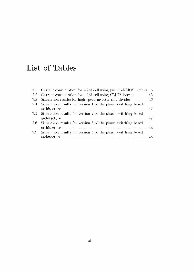
List of Tables
7.1 Current consumption for ÷2/3 cell using pseudo-NMOS latches 457.2 Current consumption for ÷2/3 cell using CMOS latches . . . . 457.3 Simulation results for high-speed inverter ring divider . . . . . 467.4 Simulation results for version 1 of the phase switching based
architecture . . . . . . . . . . . . . . . . . . . . . . . . . . . . 477.5 Simulation results for version 2 of the phase switching based
architecture . . . . . . . . . . . . . . . . . . . . . . . . . . . . 477.6 Simulation results for version 3 of the phase switching based
architecture . . . . . . . . . . . . . . . . . . . . . . . . . . . . 487.7 Simulation results for version 4 of the phase switching based
architecture . . . . . . . . . . . . . . . . . . . . . . . . . . . . 48
xi

xii LIST OF TABLES
Chapter 1
Introduction
A prescaler is an important building block in a PLL, where it divides the VCOfrequency to a lower frequency before the phase detector. A multi-modulusprescaler will typically be used in a fractional-N synthesizer (in which theseparation between the output frequencies can be given as a fraction of theinput frequency) to acheive very good resolution in frequency, and at thesame time have a high PLL bandwidth.
A 5.8 GHz 64-modulus prescaler for use in a ISM band transceiver, isto be designed in a 0.18 µm CMOS process. One of the main challengeswill be to acheive the wanted operation at high enough frequency. Di�erentapproaches will be tried out, in order to �nd the best architecture possible.An architecture based on a chain of identical ÷2/3 cells with local feedbackpresented by Cicero S. Vaucher et al. in [1], and one utilizing an interestingphase switching technique presented by Michael H. Perrott in his PhD thesisfrom MIT [2], are two approaches that will be investigated closer.
1

2 CHAPTER 1. INTRODUCTION
Chapter 2
Background Theory
2.1 Basic Circuits
2.1.1 The Johnson Counter (÷2)
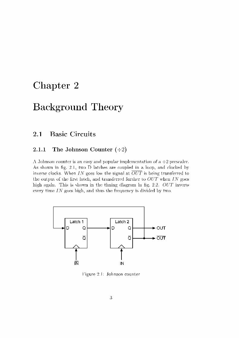
A Johnson counter is an easy and popular implementation of a ÷2 prescaler.As shown in �g. 2.1, two D latches are coupled in a loop, and clocked byinverse clocks. When IN goes low the signal at OUT is being transferred tothe output of the �rst latch, and transferred further to OUT when IN goeshigh again. This is shown in the timing diagram in �g. 2.2. OUT invertsevery time IN goes high, and thus the frequency is divided by two.
Figure 2.1: Johnson counter
3
4 CHAPTER 2. BACKGROUND THEORY
Figure 2.2: Timing diagram for Johnson counter
2.1.2 ÷3 Circuit
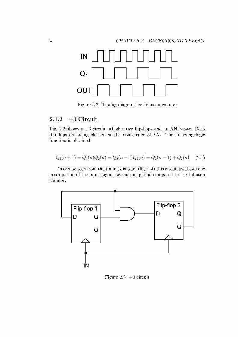
Fig. 2.3 shows a ÷3 circuit utilizing two �ip-�ops and an AND-gate. Both�ip-�ops are being clocked at the rising edge of IN . The following logicfunction is obtained:
Q2(n + 1) = Q1(n)Q2(n) = Q2(n− 1)Q2(n) = Q2(n− 1) + Q2(n) (2.1)
As can be seen from the timing diagram (�g. 2.4) this circuit swallows oneextra period of the input signal per output period compared to the Johnsoncounter.
Figure 2.3: ÷3 circuit
2.1. BASIC CIRCUITS 5
Figure 2.4: Timing diagram for ÷3 circuit
2.1.3 Dual-Modulus ÷2/3 Circuit
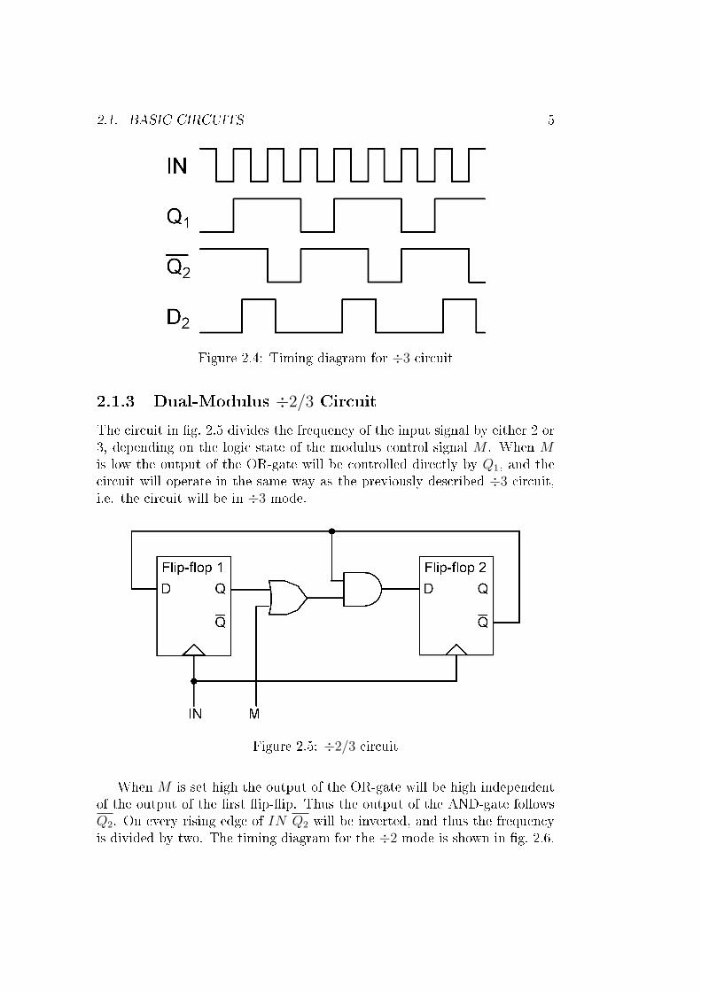
The circuit in �g. 2.5 divides the frequency of the input signal by either 2 or3, depending on the logic state of the modulus control signal M . When Mis low the output of the OR-gate will be controlled directly by Q1, and thecircuit will operate in the same way as the previously described ÷3 circuit,i.e. the circuit will be in ÷3 mode.
Figure 2.5: ÷2/3 circuit
When M is set high the output of the OR-gate will be high independentof the output of the �rst �ip-�ip. Thus the output of the AND-gate followsQ2. On every rising edge of IN Q2 will be inverted, and thus the frequencyis divided by two. The timing diagram for the ÷2 mode is shown in �g. 2.6.
6 CHAPTER 2. BACKGROUND THEORY
Figure 2.6: Timing diagram for ÷2/3 circuit in ÷2 mode (M = 1)
2.2 Multi-Modulus Circuits
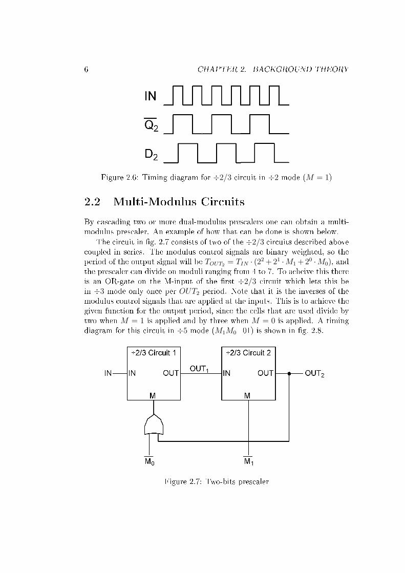
By cascading two or more dual-modulus prescalers one can obtain a multi-modulus prescaler. An example of how that can be done is shown below.
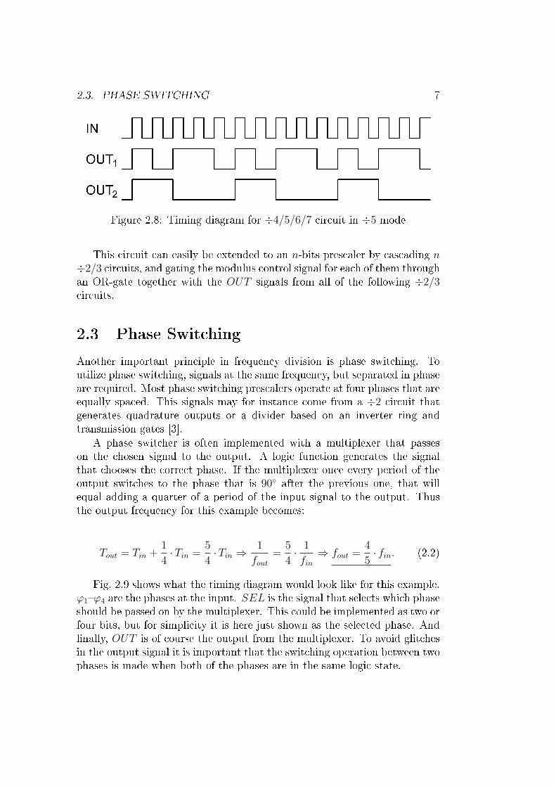
The circuit in �g. 2.7 consists of two of the ÷2/3 circuits described abovecoupled in series. The modulus control signals are binary weighted, so theperiod of the output signal will be TOUT2 = TIN · (22 + 21 ·M1 + 20 ·M0), andthe prescaler can divide on moduli ranging from 4 to 7. To acheive this thereis an OR-gate on the M-input of the �rst ÷2/3 circuit which lets this bein ÷3 mode only once per OUT2 period. Note that it is the inverses of themodulus control signals that are applied at the inputs. This is to achieve thegiven function for the output period, since the cells that are used divide bytwo when M = 1 is applied and by three when M = 0 is applied. A timingdiagram for this circuit in ÷5 mode (M1M0=01) is shown in �g. 2.8.
Figure 2.7: Two-bits prescaler
2.3. PHASE SWITCHING 7
Figure 2.8: Timing diagram for ÷4/5/6/7 circuit in ÷5 mode
This circuit can easily be extended to an n-bits prescaler by cascading n÷2/3 circuits, and gating the modulus control signal for each of them throughan OR-gate together with the OUT signals from all of the following ÷2/3circuits.
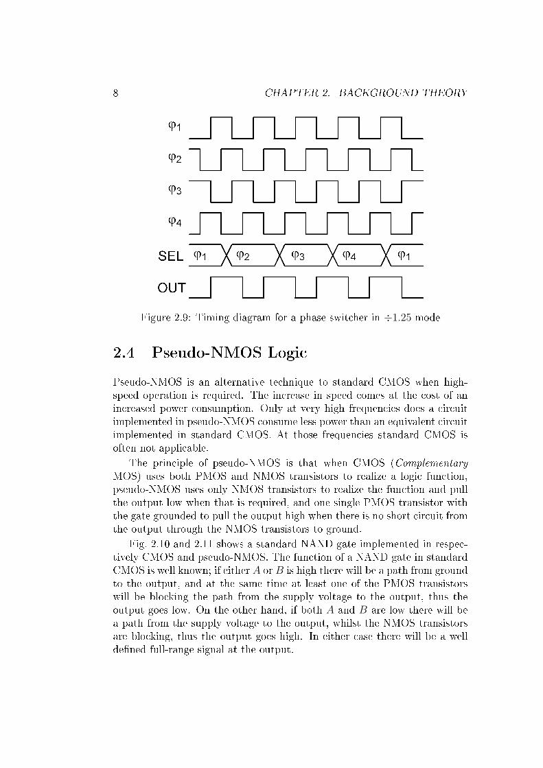
2.3 Phase Switching
Another important principle in frequency division is phase switching. Toutilize phase switching, signals at the same frequency, but separated in phaseare required. Most phase switching prescalers operate at four phases that areequally spaced. This signals may for instance come from a ÷2 circuit thatgenerates quadrature outputs or a divider based on an inverter ring andtransmission gates [3].
A phase switcher is often implemented with a multiplexer that passeson the chosen signal to the output. A logic function generates the signalthat chooses the correct phase. If the multiplexer once every period of theoutput switches to the phase that is 90◦ after the previous one, that willequal adding a quarter of a period of the input signal to the output. Thusthe output frequency for this example becomes:
Tout = Tin +1
4·Tin =
5
4·Tin ⇒
1
fout
=5
4· 1
fin
⇒ fout =4
5· fin. (2.2)
Fig. 2.9 shows what the timing diagram would look like for this example.ϕ1�ϕ4 are the phases at the input. SEL is the signal that selects which phaseshould be passed on by the multiplexer. This could be implemented as two orfour bits, but for simplicity it is here just shown as the selected phase. And�nally, OUT is of course the output from the multiplexer. To avoid glitchesin the output signal it is important that the switching operation between twophases is made when both of the phases are in the same logic state.
8 CHAPTER 2. BACKGROUND THEORY
Figure 2.9: Timing diagram for a phase switcher in ÷1.25 mode
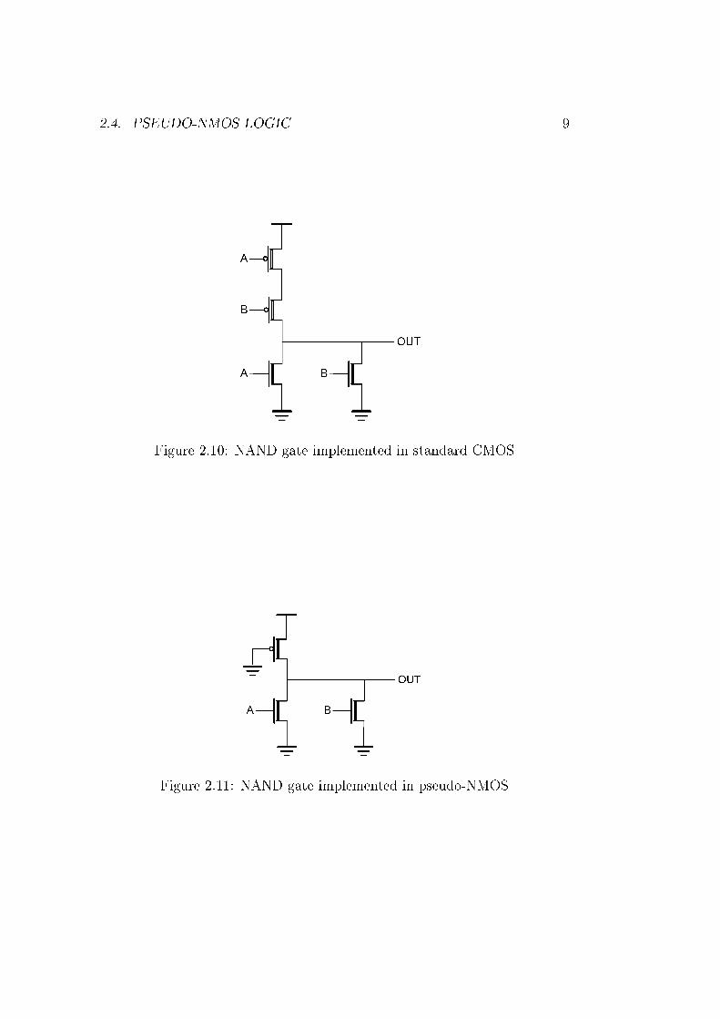
2.4 Pseudo-NMOS Logic
Pseudo-NMOS is an alternative technique to standard CMOS when high-speed operation is required. The increase in speed comes at the cost of anincreased power consumption. Only at very high frequencies does a circuitimplemented in pseudo-NMOS consume less power than an equivalent circuitimplemented in standard CMOS. At those frequencies standard CMOS isoften not applicable.
The principle of pseudo-NMOS is that when CMOS (Complementary
MOS) uses both PMOS and NMOS transistors to realize a logic function,pseudo-NMOS uses only NMOS transistors to realize the function and pullthe output low when that is required, and one single PMOS transistor withthe gate grounded to pull the output high when there is no short circuit fromthe output through the NMOS transistors to ground.
Fig. 2.10 and 2.11 shows a standard NAND gate implemented in respec-tively CMOS and pseudo-NMOS. The function of a NAND gate in standardCMOS is well known; if either A or B is high there will be a path from groundto the output, and at the same time at least one of the PMOS transistorswill be blocking the path from the supply voltage to the output, thus theoutput goes low. On the other hand, if both A and B are low there will bea path from the supply voltage to the output, whilst the NMOS transistorsare blocking, thus the output goes high. In either case there will be a wellde�ned full-range signal at the output.
2.4. PSEUDO-NMOS LOGIC 9
Figure 2.10: NAND gate implemented in standard CMOS
Figure 2.11: NAND gate implemented in pseudo-NMOS
10 CHAPTER 2. BACKGROUND THEORY
The behaviour of the pseudo-NMOS gate is not very di�erent. If bothinputs are low the NMOS transistors will block, whilst the gate-groundedPMOS transistor leads, and the output is pulled up to the level of the supplyvoltage. On the contrary, if one of the inputs are high there will be a pathbetween ground and the output. At the same time there will also be apath from the supply voltage to the output, since the gate of the PMOS isgrounded and hence leading constantly. The output voltage is thus given bythe ratio of the resistances from the output to ground and the supply voltagerespectively.
In a standard CMOS logical circuit each input is connected to the gateof both a PMOS and an NMOS transistor. In pseudo-NMOS it is onlyconnected to the gate of an NMOS. This reduces the input capacitance,and thus increases the maximum speed. This increase in speed comes atthe expense of a reduction in the signal swing. Pseudo-NMOS also consumesmore power than CMOS for operation at low and moderate frequencies. Thatis because there will be a constant, relatively high current pull from supplyto ground while the NMOS transistors are leading.
Chapter 3
÷2/3 Cells With Local Feedback
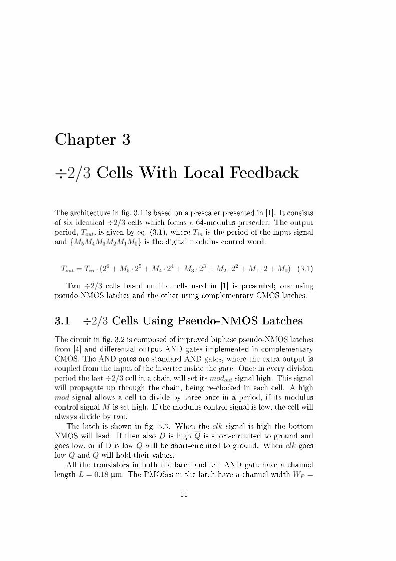
The architecture in �g. 3.1 is based on a prescaler presented in [1]. It consistsof six identical ÷2/3 cells which forms a 64-modulus prescaler. The outputperiod, Tout, is given by eq. (3.1), where Tin is the period of the input signaland {M5M4M3M2M1M0} is the digital modulus control word.
Tout = Tin · (26 + M5 · 25 + M4 · 24 + M3 · 23 + M2 · 22 + M1 · 2 + M0) (3.1)
Two ÷2/3 cells based on the cells used in [1] is presented; one usingpseudo-NMOS latches and the other using complementary CMOS latches.
3.1 ÷2/3 Cells Using Pseudo-NMOS Latches
The circuit in �g. 3.2 is composed of improved biphase pseudo-NMOS latchesfrom [4] and di�erential output AND gates implemented in complementaryCMOS. The AND gates are standard AND gates, where the extra output iscoupled from the input of the inverter inside the gate. Once in every divisionperiod the last ÷2/3 cell in a chain will set its modout signal high. This signalwill propagate up through the chain, being re-clocked in each cell. A highmod signal allows a cell to divide by three once in a period, if its moduluscontrol signal M is set high. If the modulus control signal is low, the cell willalways divide by two.
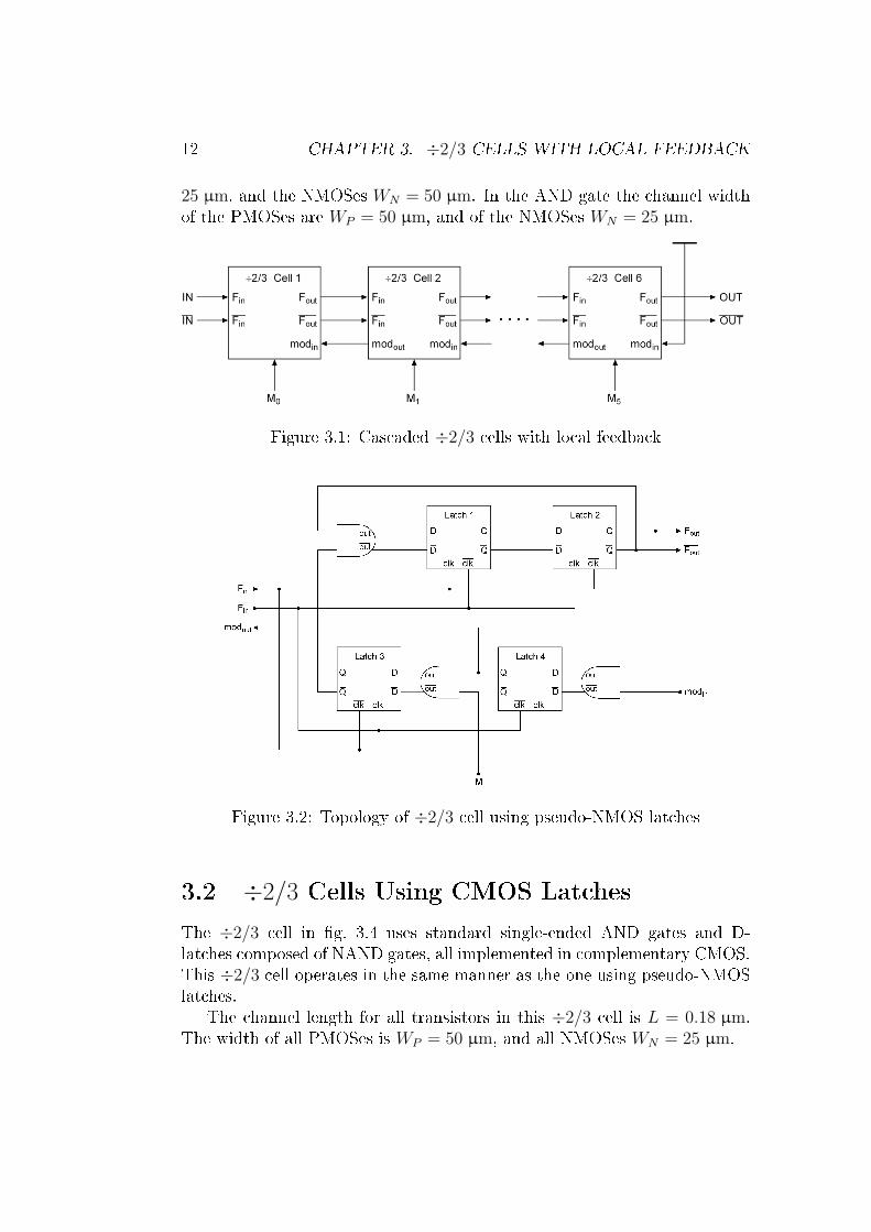
The latch is shown in �g. 3.3. When the clk signal is high the bottomNMOS will lead. If then also D is high Q is short-circuited to ground andgoes low, or if D is low Q will be short-circuited to ground. When clk goeslow Q and Q will hold their values.
All the transistors in both the latch and the AND gate have a channellength L = 0.18 µm. The PMOSes in the latch have a channel width WP =
11
12 CHAPTER 3. ÷2/3 CELLS WITH LOCAL FEEDBACK
25 µm, and the NMOSes WN = 50 µm. In the AND gate the channel widthof the PMOSes are WP = 50 µm, and of the NMOSes WN = 25 µm.
Figure 3.1: Cascaded ÷2/3 cells with local feedback
Figure 3.2: Topology of ÷2/3 cell using pseudo-NMOS latches
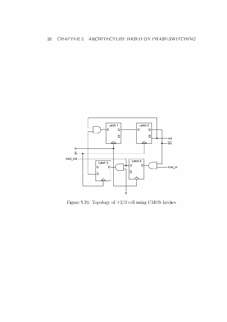
3.2 ÷2/3 Cells Using CMOS Latches
The ÷2/3 cell in �g. 3.4 uses standard single-ended AND gates and D-latches composed of NAND gates, all implemented in complementary CMOS.This ÷2/3 cell operates in the same manner as the one using pseudo-NMOSlatches.
The channel length for all transistors in this ÷2/3 cell is L = 0.18 µm.The width of all PMOSes is WP = 50 µm, and all NMOSes WN = 25 µm.
3.2. ÷2/3 CELLS USING CMOS LATCHES 13
Figure 3.3: Implementation of an improved biphase pseudo-NMOS latch
Figure 3.4: Topology of ÷2/3 cell using CMOS latches

14 CHAPTER 3. ÷2/3 CELLS WITH LOCAL FEEDBACK
Chapter 4
High-Speed Inverter Ring Divider
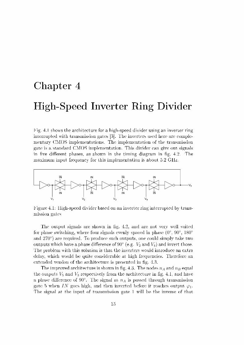
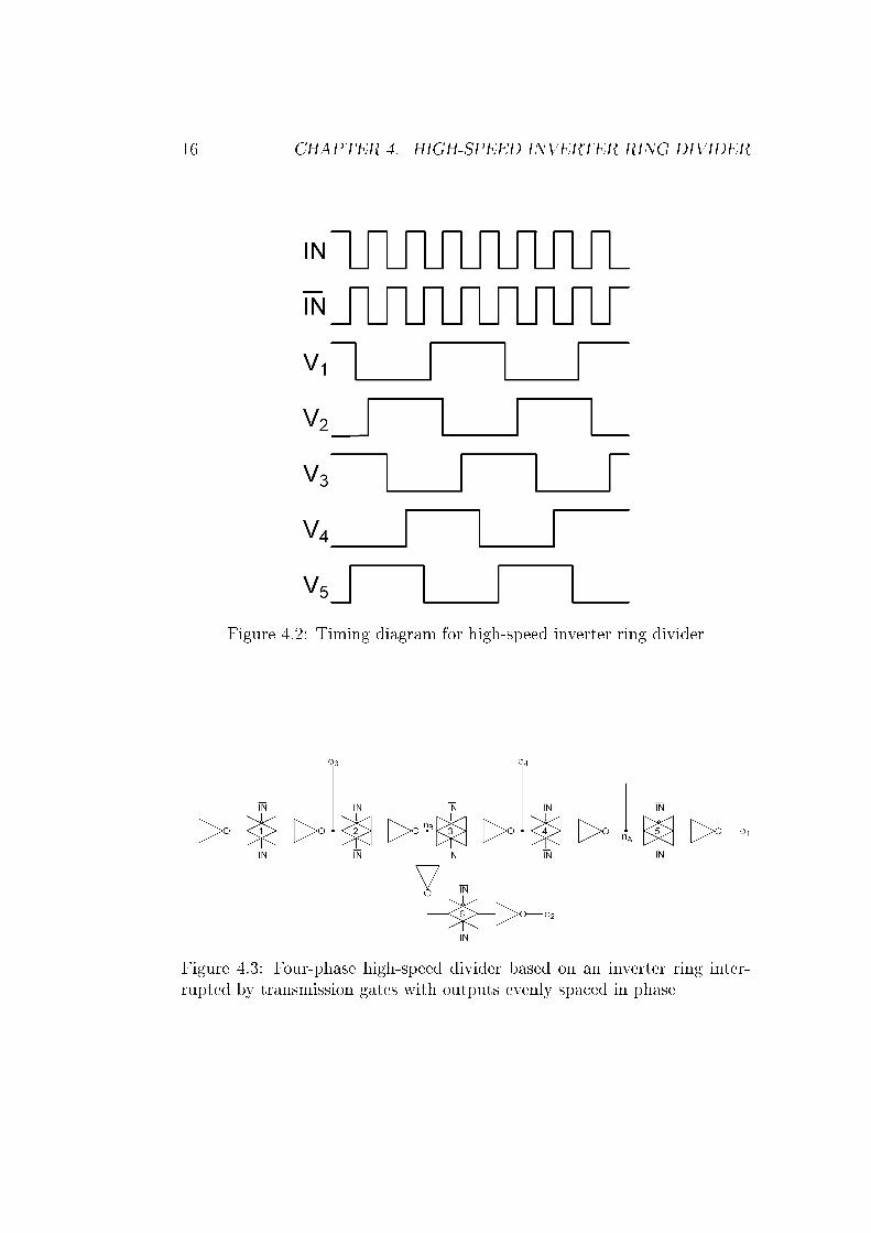
Fig. 4.1 shows the architecture for a high-speed divider using an inverter ringinterrupted with transmission gates [3]. The inverters used here are comple-mentary CMOS implementations. The implementation of the transmissiongate is a standard CMOS implementation. This divider can give out signalsin �ve di�erent phases, as shown in the timing diagram in �g. 4.2. Themaximum input frequency for this implementation is about 5.2 GHz.
Figure 4.1: High-speed divider based on an inverter ring interrupted by trans-mission gates
The output signals are shown in �g. 4.2, and are not very well suitedfor phase switching, where four signals evenly spaced in phase (0◦, 90◦, 180◦
and 270◦) are required. To produce such outputs, one could simply take twooutputs which have a phase di�erence of 90◦ (e.g. V2 and V4) and invert those.The problem with this solution is that the inverters would introduce an extradelay, which would be quite considerable at high frequencies. Therefore anextended version of the architecture is presented in �g. 4.3.
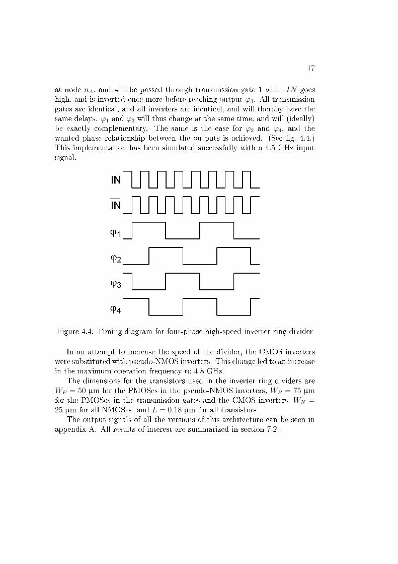
The improved architecture is shown in �g. 4.3. The nodes nA and nB equalthe outputs V5 and V3 respectively from the architecture in �g. 4.1, and havea phase di�erence of 90◦. The signal at nA is passed through transmissiongate 5 when IN goes high, and then inverted before it reaches output ϕ1.The signal at the input of transmission gate 1 will be the inverse of that
15
16 CHAPTER 4. HIGH-SPEED INVERTER RING DIVIDER
Figure 4.2: Timing diagram for high-speed inverter ring divider
Figure 4.3: Four-phase high-speed divider based on an inverter ring inter-rupted by transmission gates with outputs evenly spaced in phase
17
at node nA, and will be passed through transmission gate 1 when IN goeshigh, and is inverted once more before reaching output ϕ3. All transmissiongates are identical, and all inverters are identical, and will thereby have thesame delays. ϕ1 and ϕ3 will thus change at the same time, and will (ideally)be exactly complementary. The same is the case for ϕ2 and ϕ4, and thewanted phase relationship between the outputs is achieved. (See �g. 4.4.)This implementation has been simulated successfully with a 4.5 GHz inputsignal.
Figure 4.4: Timing diagram for four-phase high-speed inverter ring divider
In an attempt to increase the speed of the divider, the CMOS inverterswere substituted with pseudo-NMOS inverters. This change led to an increasein the maximum operation frequency to 4.8 GHz.
The dimensions for the transistors used in the inverter ring dividers areWP = 50 µm for the PMOSes in the pseudo-NMOS inverters, WP = 75 µmfor the PMOSes in the transmission gates and the CMOS inverters, WN =25 µm for all NMOSes, and L = 0.18 µm for all transistors.
The output signals of all the versions of this architecture can be seen inappendix A. All results of interest are summarized in section 7.2.

18 CHAPTER 4. HIGH-SPEED INVERTER RING DIVIDER
Chapter 5
Architecture Based on
Phase-Switching
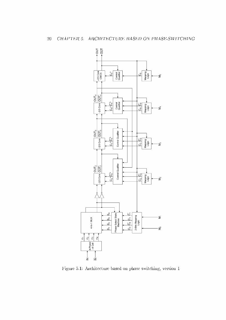
This architecture is based on a frequency divider used in Michael H. Perrott'sPhD thesis from MIT [2]. The �rst version of the architecture is just a slightmodi�cation of the original, and can be seen in �g. 5.1.
5.1 High-Speed Four-Phase ÷4 Circuit
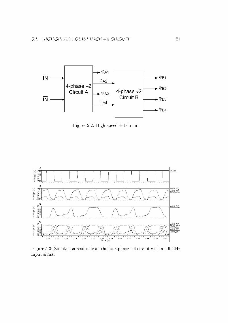
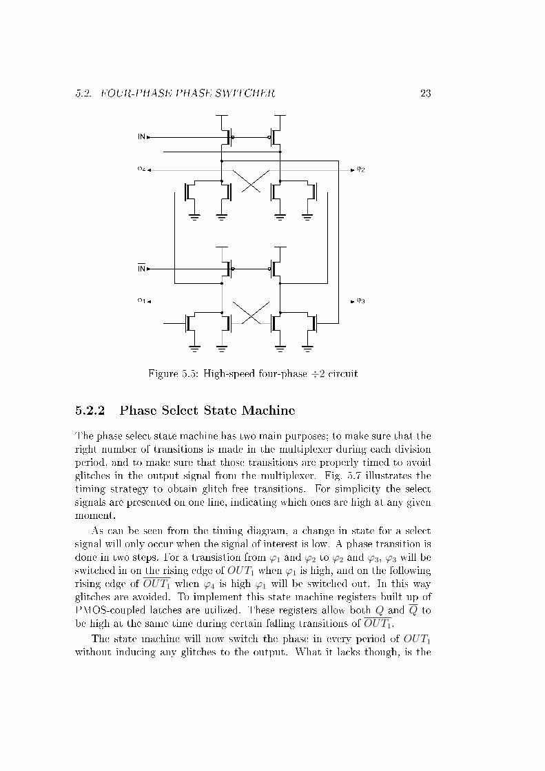
The high-speed ÷4 circuit is built up by two identical four-phase ÷2 circuits[5] connected in series, as shown in �g. 5.2. These ÷2 circuits require twocomplementary input signals to operate correctly, and give out four signalsat 0◦, 90◦, 180◦ and 270◦ phase, with a duty cycle slightly exceeding 25 %.
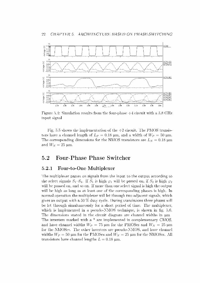
At lower frequencies this circuit would fail if the outputs ϕA2 and ϕA4 wereused directly as inputs to the next four-phase ÷2 circuit the way it is donehere. However it works very well in the input frequency range of interest,around 5.8 GHz. This is shown in the simulation plots in �g. 5.3 and �g. 5.4.The IN signal, which is exactly complementary to IN , is not shown here.Also, the ϕB1 signal is shown alone, in addition to being shown together withthe other outputs of the second ÷2 circuit, to make it easier to see the shapeof it. All the outputs of that circuit have the same shape, and are evenlyspaced in phase. As can be seen from �g. 5.3 (2.9 GHz input), the outputs ofthe second ÷2 circuits have main peaks at one fourth of the frequency of theinput, which is the wanted signal. But there are also unwanted spikes, due tothe delays from ϕA2 going low to ϕA4 going high, and from ϕA4 going low toϕA2 going high. In the case of a 5.8 GHz input these delays are signi�cantlyshorter, and as can be seen from �g. 5.4 the spikes are eliminated, and onlythe wanted signal is still there.
19
20 CHAPTER 5. ARCHITECTURE BASED ON PHASE-SWITCHING
Figure 5.1: Architecture based on phase switching, version 1
5.1. HIGH-SPEED FOUR-PHASE ÷4 CIRCUIT 21
Figure 5.2: High-speed ÷4 circuit
Figure 5.3: Simulation results from the four-phase ÷4 circuit with a 2.9 GHzinput signal
22 CHAPTER 5. ARCHITECTURE BASED ON PHASE-SWITCHING
Figure 5.4: Simulation results from the four-phase ÷4 circuit with a 5.8 GHzinput signal
Fig. 5.5 shows the implementation of the ÷2 circuit. The PMOS transis-tors have a channel length of LP = 0.18 µm, and a width of WP = 50 µm.The corresponding dimensions for the NMOS transistors are LN = 0.18 µmand WN = 25 µm.
5.2 Four-Phase Phase Switcher
5.2.1 Four-to-One Multiplexer
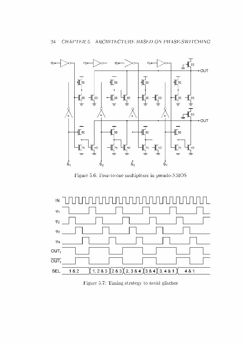
The multiplexer passes on signals from the input to the output according tothe select signals S1�S4. If S1 is high ϕ1 will be passed on, if S2 is high ϕ2
will be passed on, and so on. If more than one select signal is high the outputwill be high as long as at least one of the corresponding phases is high. Innormal operation the multiplexer will let through two adjacent signals, whichgives an output with a 50 % duty cycle. During transistions three phases willbe let through simultaneously for a short period of time. The multiplexer,which is implemented in a pseudo-NMOS technique, is shown in �g. 5.6.The dimensions stated in the circuit diagram are channel widths in µmThe inverters marked with a * are implemented in complementary CMOS,and have channel widths WP = 75 µm for the PMOSes and WN = 25 µmfor the NMOSes. The other inverters are pseudo-NMOS, and have channelwidths WP = 50 µm for the PMOSes and WN = 25 µm for the NMOSes. Alltransistors have channel lengths L = 0.18 µm.
5.2. FOUR-PHASE PHASE SWITCHER 23
Figure 5.5: High-speed four-phase ÷2 circuit
5.2.2 Phase Select State Machine
The phase select state machine has two main purposes; to make sure that theright number of transitions is made in the multiplexer during each divisionperiod, and to make sure that those transitions are properly timed to avoidglitches in the output signal from the multiplexer. Fig. 5.7 illustrates thetiming strategy to obtain glitch-free transitions. For simplicity the selectsignals are presented on one line, indicating which ones are high at any givenmoment.
As can be seen from the timing diagram, a change in state for a selectsignal will only occur when the signal of interest is low. A phase transition isdone in two steps. For a transistion from ϕ1 and ϕ2 to ϕ2 and ϕ3, ϕ3 will beswitched in on the rising edge of OUT1 when ϕ1 is high, and on the followingrising edge of OUT1 when ϕ4 is high ϕ1 will be switched out. In this wayglitches are avoided. To implement this state machine registers built up ofPMOS-coupled latches are utilized. These registers allow both Q and Q tobe high at the same time during certain falling transitions of OUT1.
The state machine will now switch the phase in every period of OUT1
without inducing any glitches to the output. What it lacks though, is the
24 CHAPTER 5. ARCHITECTURE BASED ON PHASE-SWITCHING
Figure 5.6: Four-to-one multiplexer in pseudo-NMOS
Figure 5.7: Timing strategy to avoid glitches
5.2. FOUR-PHASE PHASE SWITCHER 25
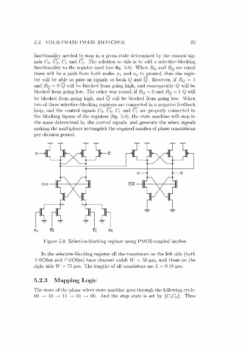
functionality needed to stop in a given state determined by the control sig-nals C0, C0, C1 and C1. The solution to this is to add a selective-blockingfunctionality to the register used (see �g. 5.8). When BQ and BQ are equalthere will be a path from both nodes n1 and n2 to ground, thus the regis-ter will be able to pass on signals to both Q and Q. However, if BQ = 1and BQ = 0 Q will be blocked from going high, and consequently Q will beblocked from going low. The other way round, if BQ = 0 and BQ = 1 Q will
be blocked from going high, and Q will be blocked from going low. Whentwo of these selective-blocking registers are connected in a negative feedbackloop, and the control signals C0, C0, C1 and C1 are properly connected tothe blocking inputs of the registers (�g. 5.9), the state machine will stop inthe state determined by the control signals, and generate the select signalsmaking the multiplexer accomplish the required number of phase transistionsper division period.
Figure 5.8: Selective-blocking register using PMOS-coupled latches
In the selective-blocking register all the transistors on the left side (bothNMOSes and PMOSes) have channel width W = 50 µm, and those on theright side W = 75 µm. The lengths of all transistors are L = 0.18 µm.
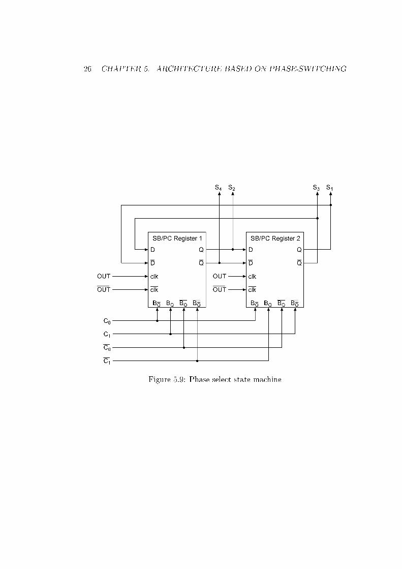
5.2.3 Mapping Logic
The state of the phase select state machine goes through the following cycle:00 → 10 → 11 → 01 → 00. And the stop state is set by {C1C0}. Thus
26 CHAPTER 5. ARCHITECTURE BASED ON PHASE-SWITCHING
Figure 5.9: Phase select state machine
5.3. ÷2/3 STAGES 27
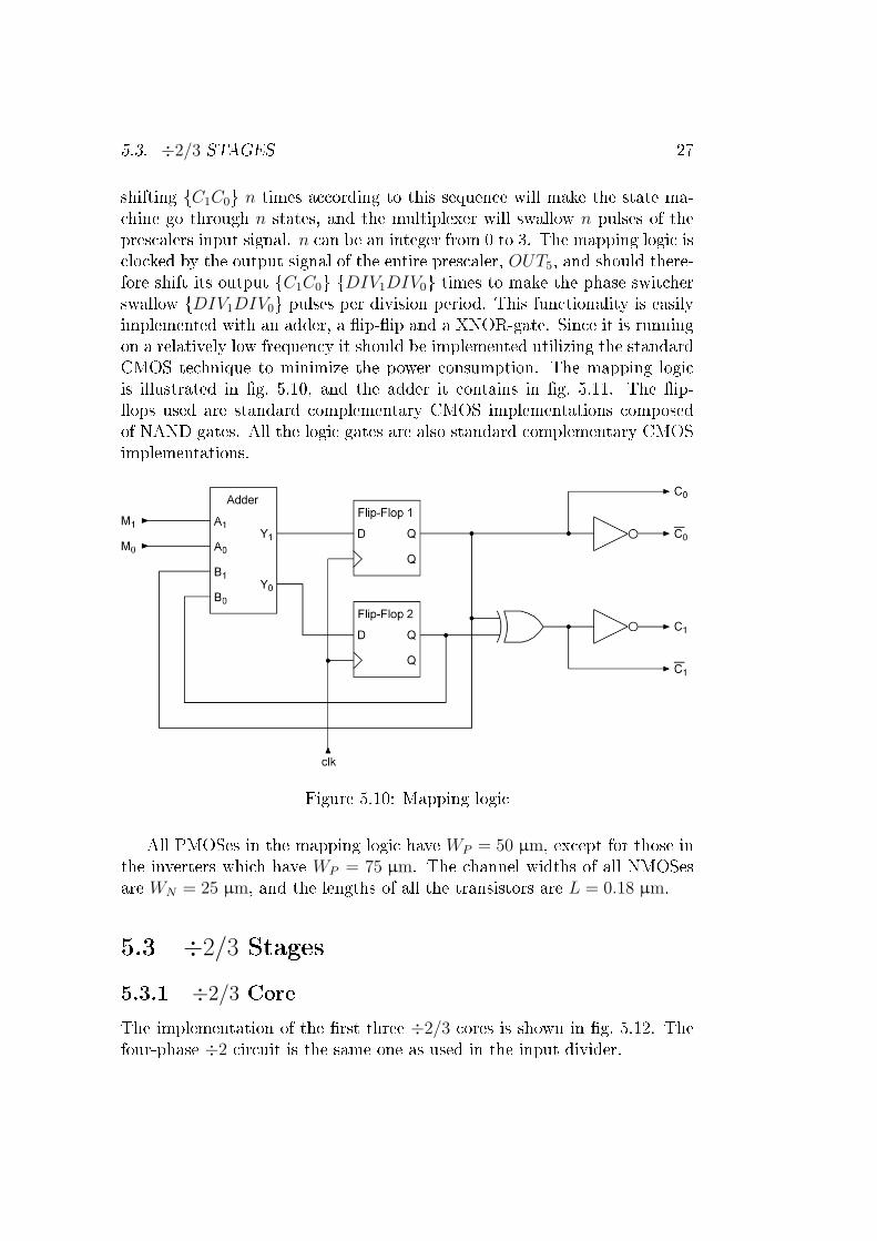
shifting {C1C0} n times according to this sequence will make the state ma-chine go through n states, and the multiplexer will swallow n pulses of theprescalers input signal. n can be an integer from 0 to 3. The mapping logic isclocked by the output signal of the entire prescaler, OUT5, and should there-fore shift its output {C1C0} {DIV1DIV0} times to make the phase switcherswallow {DIV1DIV0} pulses per division period. This functionality is easilyimplemented with an adder, a �ip-�ip and a XNOR-gate. Since it is runningon a relatively low frequency it should be implemented utilizing the standardCMOS technique to minimize the power consumption. The mapping logicis illustrated in �g. 5.10, and the adder it contains in �g. 5.11. The �ip-�ops used are standard complementary CMOS implementations composedof NAND gates. All the logic gates are also standard complementary CMOSimplementations.
Figure 5.10: Mapping logic
All PMOSes in the mapping logic have WP = 50 µm, except for those inthe inverters which have WP = 75 µm. The channel widths of all NMOSesare WN = 25 µm, and the lengths of all the transistors are L = 0.18 µm.
5.3 ÷2/3 Stages
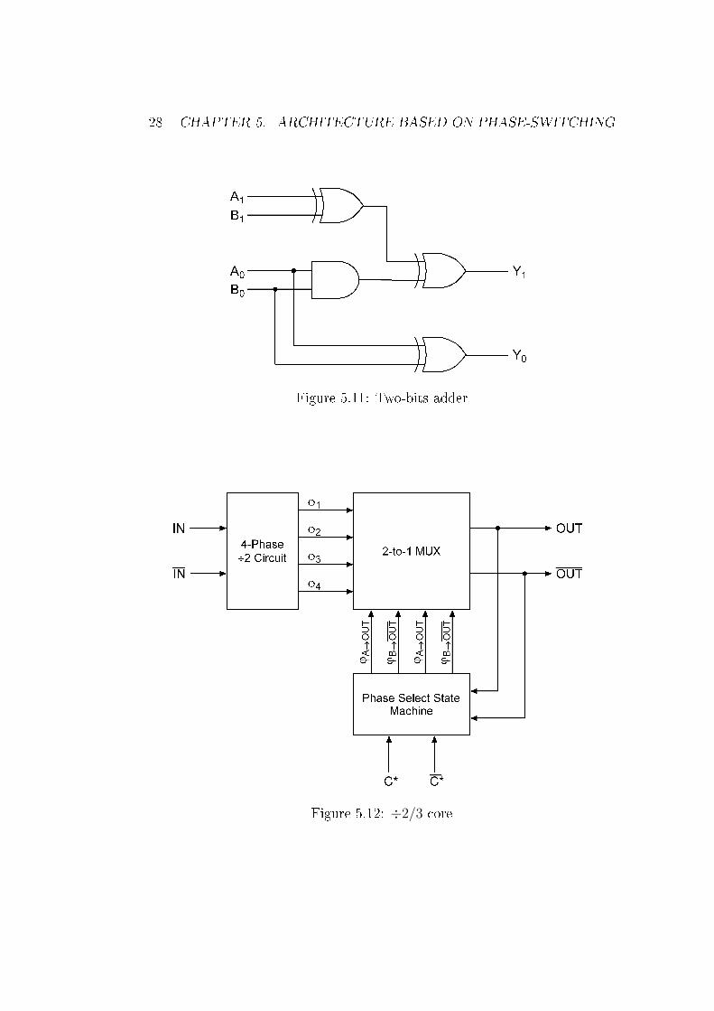
5.3.1 ÷2/3 Core
The implementation of the �rst three ÷2/3 cores is shown in �g. 5.12. Thefour-phase ÷2 circuit is the same one as used in the input divider.
28 CHAPTER 5. ARCHITECTURE BASED ON PHASE-SWITCHING
Figure 5.11: Two-bits adder
Figure 5.12: ÷2/3 core
5.3. ÷2/3 STAGES 29
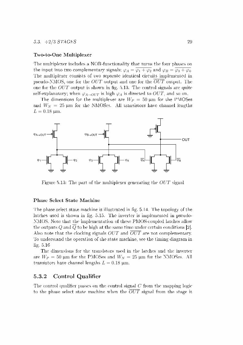
Two-to-One Multiplexer
The multiplexer includes a NOR-functionality that turns the four phases onthe input into two complementary signals; ϕA = ϕ1 + ϕ2 and ϕB = ϕ3 + ϕ4.The multiplexer consists of two separate identical circuits implemented inpseudo-NMOS, one for the OUT output and one for the OUT output. Theone for the OUT output is shown in �g. 5.13. The control signals are quiteself-explanatory; when ϕA→OUT is high ϕA is directed to OUT , and so on.
The dimensions for the multiplexer are WP = 50 µm for the PMOSesand WN = 25 µm for the NMOSes. All transistors have channel lengthsL = 0.18 µm.
Figure 5.13: The part of the multiplexer generating the OUT signal
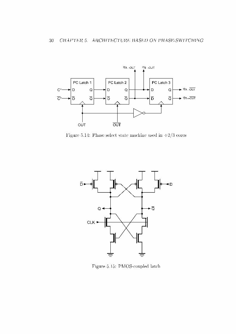
Phase Select State Machine
The phase select state machine is illustrated in �g. 5.14. The topology of thelatches used is shown in �g. 5.15. The inverter is implemented in pseudo-NMOS. Note that the implementation of these PMOS-coupled latches allowthe outputs Q and Q to be high at the same time under certain conditions [2].Also note that the clocking signals OUT and OUT are not complementary.To understand the operation of the state machine, see the timing diagram in�g. 5.16
The dimensions for the transistors used in the latches and the inverterare WP = 50 µm for the PMOSes and WN = 25 µm for the NMOSes. Alltransistors have channel lengths L = 0.18 µm.
5.3.2 Control Quali�er
The control quali�er passes on the control signal C from the mapping logicto the phase select state machine when the OUT signal from the stage it
30 CHAPTER 5. ARCHITECTURE BASED ON PHASE-SWITCHING
Figure 5.14: Phase select state machine used in ÷2/3 cores
Figure 5.15: PMOS-coupled latch
5.3. ÷2/3 STAGES 31
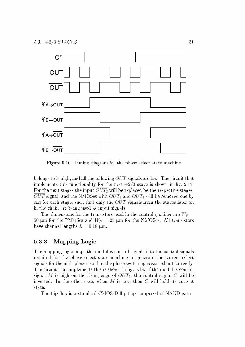
Figure 5.16: Timing diagram for the phase select state machine
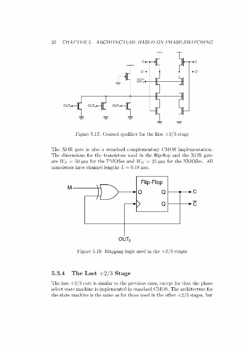
belongs to is high, and all the following OUT signals are low. The circuit thatimplements this functionality for the �rst ÷2/3 stage is shown in �g. 5.17.For the next stages the input OUT2 will be replaced be the respective stages'OUT signal, and the NMOSes with OUT3 and OUT4 will be removed one byone for each stage, such that only the OUT signals from the stages later onin the chain are being used as input signals.
The dimensions for the transistors used in the control quali�er are WP =50 µm for the PMOSes and WN = 25 µm for the NMOSes. All transistorshave channel lengths L = 0.18 µm.
5.3.3 Mapping Logic
The mapping logic maps the modulus control signals into the control signalsrequired for the phase select state machine to generate the correct selectsignals for the multiplexer, so that the phase switching is carried out correctly.The circuit that implements this is shown in �g. 5.18. If the modulus controlsignal M is high on the rising edge of OUT5, the control signal C will beinverted. In the other case, when M is low, then C will hold its currentstate.
The �ip-�op is a standard CMOS D-�ip-�op composed of NAND gates.
32 CHAPTER 5. ARCHITECTURE BASED ON PHASE-SWITCHING
Figure 5.17: Control quali�er for the �rst ÷2/3 stage
The XOR gate is also a standard complementary CMOS implementation.The dimensions for the transistors used in the �ip-�op and the XOR gateare WP = 50 µm for the PMOSes and WN = 25 µm for the NMOSes. Alltransistors have channel lengths L = 0.18 µm.
Figure 5.18: Mapping logic used in the ÷2/3 stages
5.3.4 The Last ÷2/3 Stage
The last ÷2/3 core is similar to the previous ones, except for that the phaseselect state machine is implemented in standard CMOS. The architecture forthe state machine is the same as for those used in the other ÷2/3 stages, but
5.4. VERSION 2 � ÷2/3 CELLS WITH LOCAL FEEDBACK 33
the latches and the inverter are implemented in complementary CMOS. Thechannel widths for the PMOSes used in the latches are WP = 50 µm, andfor the PMOS in the inverter WP = 75 µm. All NMOSes have WN = 25 µm.All transistors have channel lengths L = 0.18 µm.
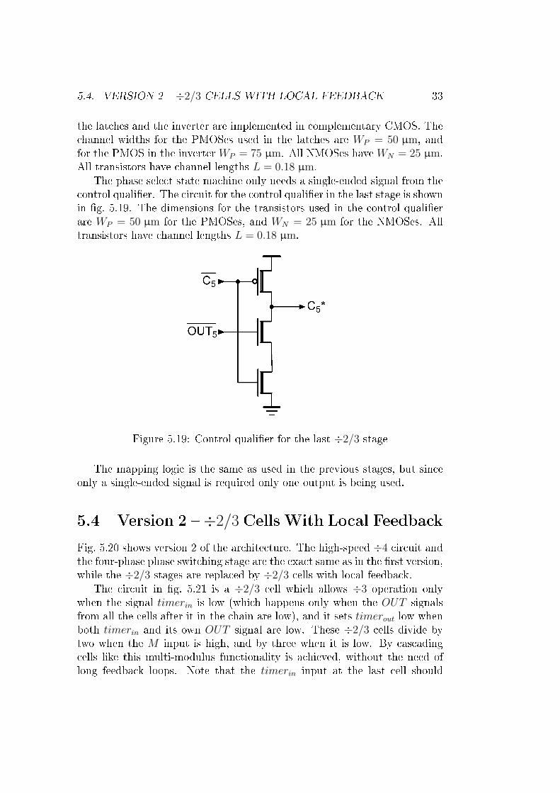
The phase select state machine only needs a single-ended signal from thecontrol quali�er. The circuit for the control quali�er in the last stage is shownin �g. 5.19. The dimensions for the transistors used in the control quali�erare WP = 50 µm for the PMOSes, and WN = 25 µm for the NMOSes. Alltransistors have channel lengths L = 0.18 µm.
Figure 5.19: Control quali�er for the last ÷2/3 stage
The mapping logic is the same as used in the previous stages, but sinceonly a single-ended signal is required only one output is being used.
5.4 Version 2 � ÷2/3 Cells With Local Feedback
Fig. 5.20 shows version 2 of the architecture. The high-speed ÷4 circuit andthe four-phase phase switching stage are the exact same as in the �rst version,while the ÷2/3 stages are replaced by ÷2/3 cells with local feedback.
The circuit in �g. 5.21 is a ÷2/3 cell which allows ÷3 operation onlywhen the signal timerin is low (which happens only when the OUT signalsfrom all the cells after it in the chain are low), and it sets timerout low whenboth timerin and its own OUT signal are low. These ÷2/3 cells divide bytwo when the M input is high, and by three when it is low. By cascadingcells like this multi-modulus functionality is achieved, without the need oflong feedback loops. Note that the timerin input at the last cell should
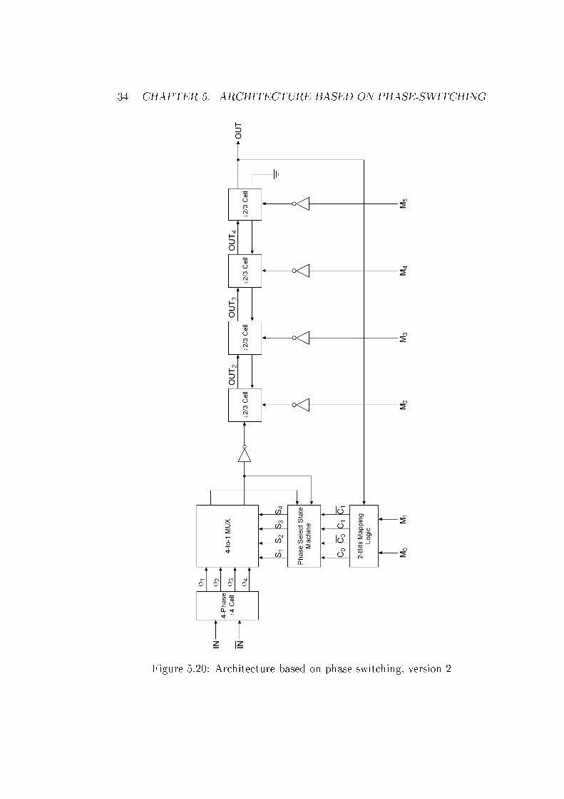
34 CHAPTER 5. ARCHITECTURE BASED ON PHASE-SWITCHING
Figure 5.20: Architecture based on phase switching, version 2
5.5. VERSION 3 � FOUR-TO-ONEMULTIPLEXER IMPLEMENTED IN CMOS35
be connected to ground. The �ip-�ops and the logic gates are standardcomplementary CMOS implementations.
The channel widths for all PMOSes, except the one in the inverter, areWP = 50 µm, and for the PMOS in the inverter WP = 75 µm. All NMOSeshave WN = 25 µm. All transistors have channel lengths L = 0.18 µm.
Figure 5.21: ÷2/3 cell with local feedback
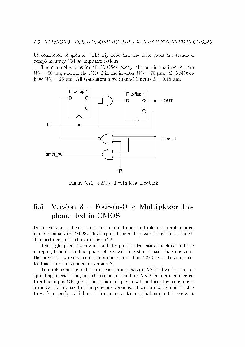
5.5 Version 3 � Four-to-One Multiplexer Im-
plemented in CMOS
In this version of the architecture the four-to-one multiplexer is implementedin complementary CMOS. The output of the multiplexer is now single-ended.The architecture is shown in �g. 5.22.
The high-speed ÷4 circuit, and the phase select state machine and themapping logic in the four-phase phase switching stage is still the same as inthe previous two versions of the architecture. The ÷2/3 cells utilizing localfeedback are the same as in version 2.
To implement the multiplexer each input phase is AND-ed with its corre-sponding select signal, and the output of the four AND gates are connectedto a four-input OR gate. Thus this multiplexer will perform the same oper-ation as the one used in the previous versions. It will probably not be ableto work properly as high up in frequency as the original one, but it works at
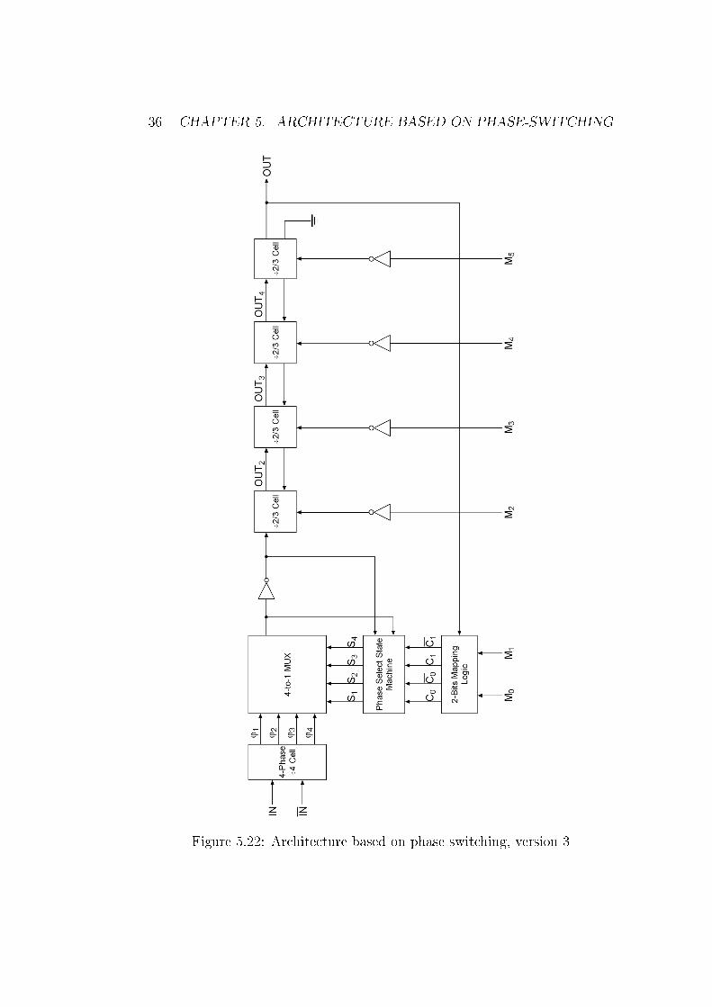
36 CHAPTER 5. ARCHITECTURE BASED ON PHASE-SWITCHING
Figure 5.22: Architecture based on phase switching, version 3
5.6. VERSION 4 � ALTERNATIVE LOCAL FEEDBACK ÷2/3 CELL 37
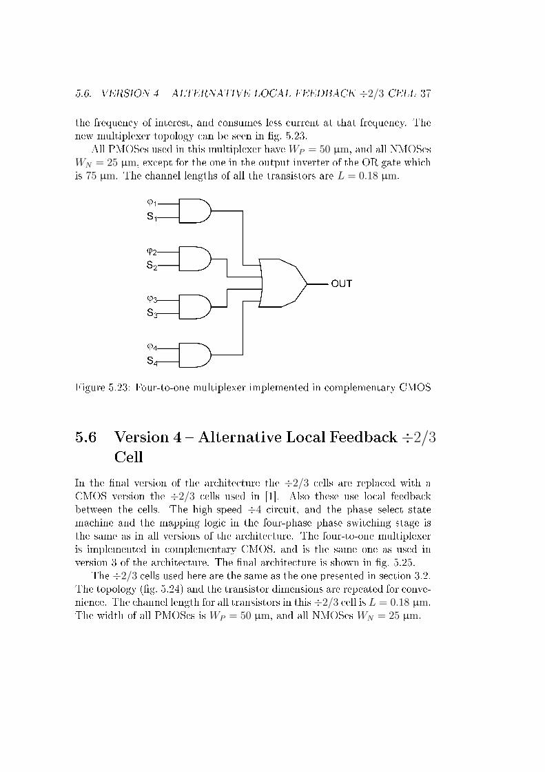
the frequency of interest, and consumes less current at that frequency. Thenew multiplexer topology can be seen in �g. 5.23.
All PMOSes used in this multiplexer have WP = 50 µm, and all NMOSesWN = 25 µm, except for the one in the output inverter of the OR gate whichis 75 µm. The channel lengths of all the transistors are L = 0.18 µm.
Figure 5.23: Four-to-one multiplexer implemented in complementary CMOS
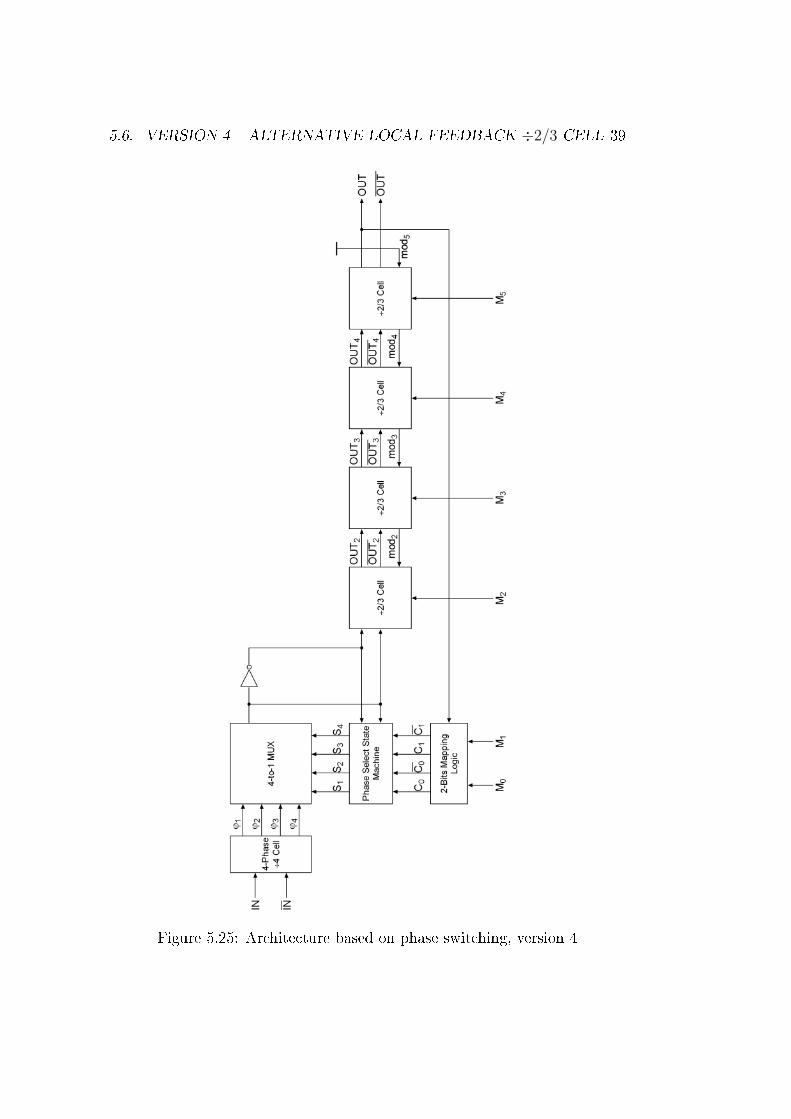
5.6 Version 4 � Alternative Local Feedback ÷2/3
Cell
In the �nal version of the architecture the ÷2/3 cells are replaced with aCMOS version the ÷2/3 cells used in [1]. Also these use local feedbackbetween the cells. The high-speed ÷4 circuit, and the phase select statemachine and the mapping logic in the four-phase phase switching stage isthe same as in all versions of the architecture. The four-to-one multiplexeris implemented in complementary CMOS, and is the same one as used inversion 3 of the architecture. The �nal architecture is shown in �g. 5.25.
The ÷2/3 cells used here are the same as the one presented in section 3.2.The topology (�g. 5.24) and the transistor dimensions are repeated for conve-nience. The channel length for all transistors in this÷2/3 cell is L = 0.18 µm.The width of all PMOSes is WP = 50 µm, and all NMOSes WN = 25 µm.
38 CHAPTER 5. ARCHITECTURE BASED ON PHASE-SWITCHING
Figure 5.24: Topology of ÷2/3 cell using CMOS latches
5.6. VERSION 4 � ALTERNATIVE LOCAL FEEDBACK ÷2/3 CELL 39
Figure 5.25: Architecture based on phase switching, version 4

40 CHAPTER 5. ARCHITECTURE BASED ON PHASE-SWITCHING
Chapter 6
Simulations
All simulations are performed with a complementary pair of square-waveinput signals applied, having a voltage swing from 0 to 1.8 V. The rise/falltime for these signals is 10 ps for all simulations. The period varies for thedi�erent simulations. The supply voltage is always 1.8 V.
6.1 ÷2/3 Cells With Local Feedback
To �nd out if any of the two presented ÷2/3 cells can be suitable for us-ing in the multi-modulus prescaler architecture shown in �g. 3.1, they are�rst simulated to �nd the maximum operation frequency when they are run-ning isolated from other circuitry. If the results from these simulations arepositive, the entire circuit should be simulated.
Both versions of the ÷2/3 cell are simulated repeatedly with gradually in-creasing frequency to �nd the highest frequency where they operate properlyin both ÷2 and ÷3 mode. The rms current consumption is also measured.The results can be found in section 7.1, and relevant simulation plots inappendix A.
6.2 High-Speed Inverter Ring Divider
The simulations that are presented for this architecture are those for themaximum operation frequencies, for the lowest frequencies where proper op-eration were not achieved, and for 1 GHz (to get a fair comparison of thecurrent consumption between the di�erent versions).
41
42 CHAPTER 6. SIMULATIONS
6.3 Architectures Based on Phase Switching
All simulations on these architectures are performed with input signals havinga period of TIN = 172.4 ps (≈ 5.8 GHz). The inputs of each bit of themodulus control word, {M5M4M3M2M1M0}, are either 0 (logical 0) or 1.8 V(logical 1). The test bench set-up is shown in �g. 6.1.
Figure 6.1: Test bench set-up
The modulus control word is binary weighted, and the period of the out-put signal is given by:
TOUT = (64 + 32M5 + 16M4 + 8M3 + 4M2 + 2M1 + M0) ·TIN (6.1)
To verify the operation of the circuits, they should ideally have beentested for every single modulus. Due to very time demanding simulationsthat is not done. Instead the circuits are tested for some chosen moduli,meant to cover the most critical operations. As long as the circuits operateproperly for these it is very likely they will also operate properly for the otherpossible moduli. A full test could be a topic for further work.
The chosen moduli are:
• {M5M4M3M2M1M0}={000000} (÷64)
• {M5M4M3M2M1M0}={000100} (÷68)
• {M5M4M3M2M1M0}={010011} (÷83)
• {M5M4M3M2M1M0}={101110} (÷110)
• {M5M4M3M2M1M0}={111001} (÷121)
• {M5M4M3M2M1M0}={111111} (÷127)

6.3. ARCHITECTURES BASED ON PHASE SWITCHING 43
The architectures in chapter 5 are simulated on this test bench, and theoutput periods and rms current consumptions of these are measured for thegiven moduli. The results from the simulations can be found in section 7.3,and the simulation plots in appendix A.

44 CHAPTER 6. SIMULATIONS
Chapter 7
Results
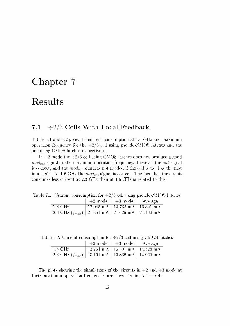
7.1 ÷2/3 Cells With Local Feedback
Tables 7.1 and 7.2 gives the current consumption at 1.6 GHz and maximumoperation frequency for the ÷2/3 cell using pseudo-NMOS latches and theone using CMOS latches respectively.
In ÷2 mode the ÷2/3 cell using CMOS latches does not produce a goodmodout signal at the maximum operation frequency. However the out signalis correct, and the modout signal is not needed if the cell is used as the �rstin a chain. At 1.6 GHz the modout signal is correct. The fact that the circuitconsumes less current at 2.3 GHz than at 1.6 GHz is related to this.
Table 7.1: Current consumption for ÷2/3 cell using pseudo-NMOS latches
÷2 mode ÷3 mode Average1.6 GHz 17.048 mA 16.733 mA 16.891 mA2.0 GHz (fmax) 21.351 mA 21.629 mA 21.490 mA
Table 7.2: Current consumption for ÷2/3 cell using CMOS latches
÷2 mode ÷3 mode Average1.6 GHz 13.754 mA 15.301 mA 14.528 mA2.3 GHz (fmax) 13.101 mA 16.836 mA 14.969 mA
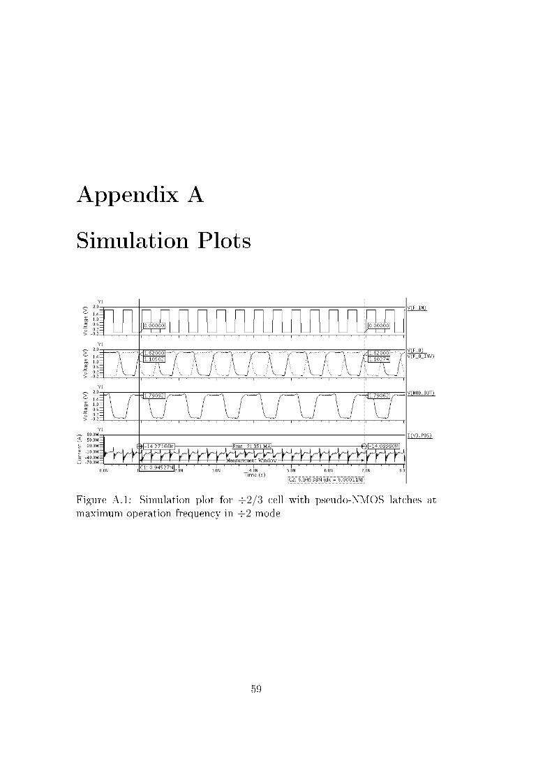
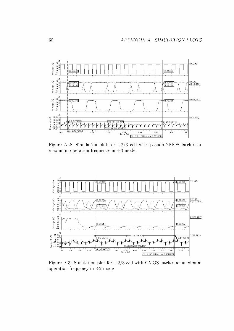
The plots showing the simulations of the circuits in ÷2 and ÷3 mode attheir maximum operation frequencies are shown in �g. A.1 � A.4.
45
46 CHAPTER 7. RESULTS
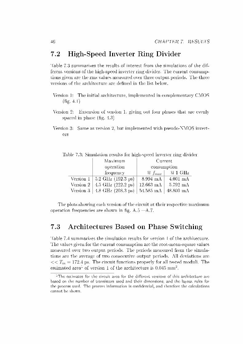
7.2 High-Speed Inverter Ring Divider
Table 7.3 summarizes the results of interest from the simulations of the dif-ferent versions of the high-speed inverter ring divider. The current consump-tions given are the rms values measured over three output periods. The threeversions of the architecture are de�ned in the list below.
Version 1: The initial architecture, implemented in complementary CMOS(�g. 4.1)
Version 2: Extension of version 1, giving out four phases that are evenlyspaced in phase (�g. 4.3)
Version 3: Same as version 2, but implemented with pseudo-NMOS invert-ers
Table 7.3: Simulation results for high-speed inverter ring divider
Maximum Currentoperation consumptionfrequency @ fmax @ 1 GHz
Version 1 5.2 GHz (192.3 ps) 8.994 mA 4.001 mAVersion 2 4.5 GHz (222.2 ps) 12.663 mA 5.792 mAVersion 3 4.8 GHz (208.3 ps) 54.585 mA 48.800 mA
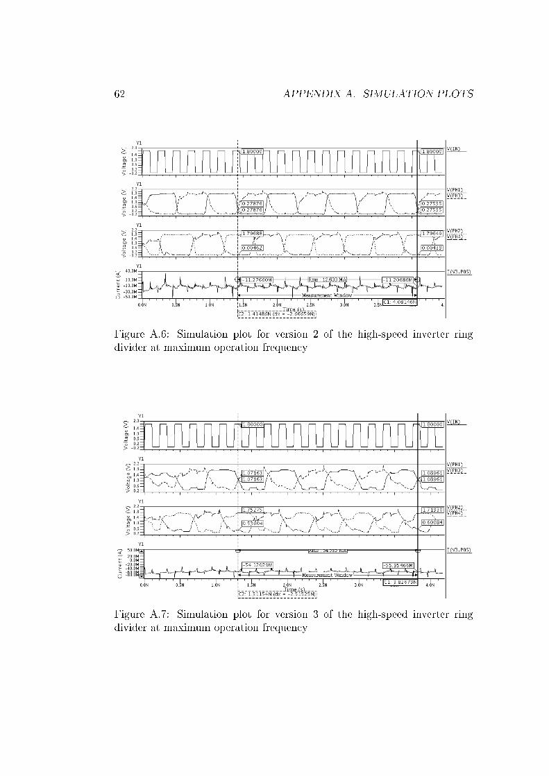
The plots showing each version of the circuit at their respective maximumoperation frequencies are shown in �g. A.5 � A.7.
7.3 Architectures Based on Phase Switching
Table 7.4 summarizes the simulation results for version 1 of the architecture.The values given for the current consumption are the root-mean-square valuesmeasured over two output periods. The periods measured from the simula-tions are the average of two consecutive output periods. All deviations are<< Tin = 172.4 ps. The circuit functions properly for all tested moduli. Theestimated area1 of version 1 of the architecture is 0.045 mm2.
1The estimates for the circuit area for the di�erent versions of this architecture are
based on the number of transistors used and their dimensions, and the layout rules for
the process used. The process information is con�dential, and therefore the calculations
cannot be shown.
7.3. ARCHITECTURES BASED ON PHASE SWITCHING 47
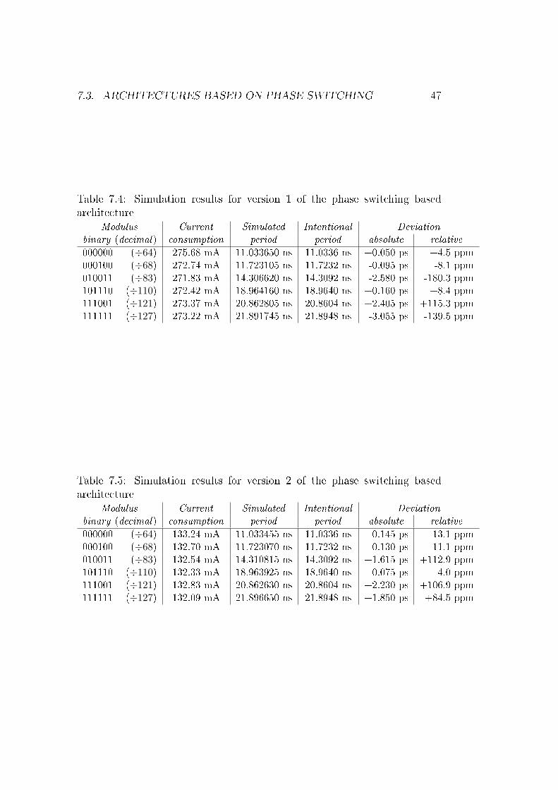
Table 7.4: Simulation results for version 1 of the phase switching basedarchitecture
Modulus Current Simulated Intentional Deviation
binary (decimal) consumption period period absolute relative
000000 (÷64) 275.68 mA 11.033650 ns 11.0336 ns +0.050 ps +4.5 ppm
000100 (÷68) 272.74 mA 11.723105 ns 11.7232 ns -0.095 ps -8.1 ppm
010011 (÷83) 271.83 mA 14.306620 ns 14.3092 ns -2.580 ps -180.3 ppm
101110 (÷110) 272.42 mA 18.964160 ns 18.9640 ns +0.160 ps +8.4 ppm
111001 (÷121) 273.37 mA 20.862805 ns 20.8604 ns +2.405 ps +115.3 ppm
111111 (÷127) 273.22 mA 21.891745 ns 21.8948 ns -3.055 ps -139.5 ppm
Table 7.5: Simulation results for version 2 of the phase switching basedarchitecture
Modulus Current Simulated Intentional Deviation
binary (decimal) consumption period period absolute relative
000000 (÷64) 133.24 mA 11.033455 ns 11.0336 ns -0.145 ps -13.1 ppm
000100 (÷68) 132.70 mA 11.723070 ns 11.7232 ns -0.130 ps -11.1 ppm
010011 (÷83) 132.54 mA 14.310815 ns 14.3092 ns +1.615 ps +112.9 ppm
101110 (÷110) 132.33 mA 18.963925 ns 18.9640 ns -0.075 ps -4.0 ppm
111001 (÷121) 132.83 mA 20.862630 ns 20.8604 ns +2.230 ps +106.9 ppm
111111 (÷127) 132.09 mA 21.896650 ns 21.8948 ns +1.850 ps +84.5 ppm
48 CHAPTER 7. RESULTS
Table 7.5 summarizes the simulation results for version 2 of the architec-ture. The values given for the current consumption are the root-mean-squarevalues measured over two output periods. The periods measured from thesimulations are the average of two consecutive output periods. All deviationsare << Tin = 172.4 ps. The circuit functions properly for all tested moduli.The estimated area of version 2 of the architecture is 0.039 mm2
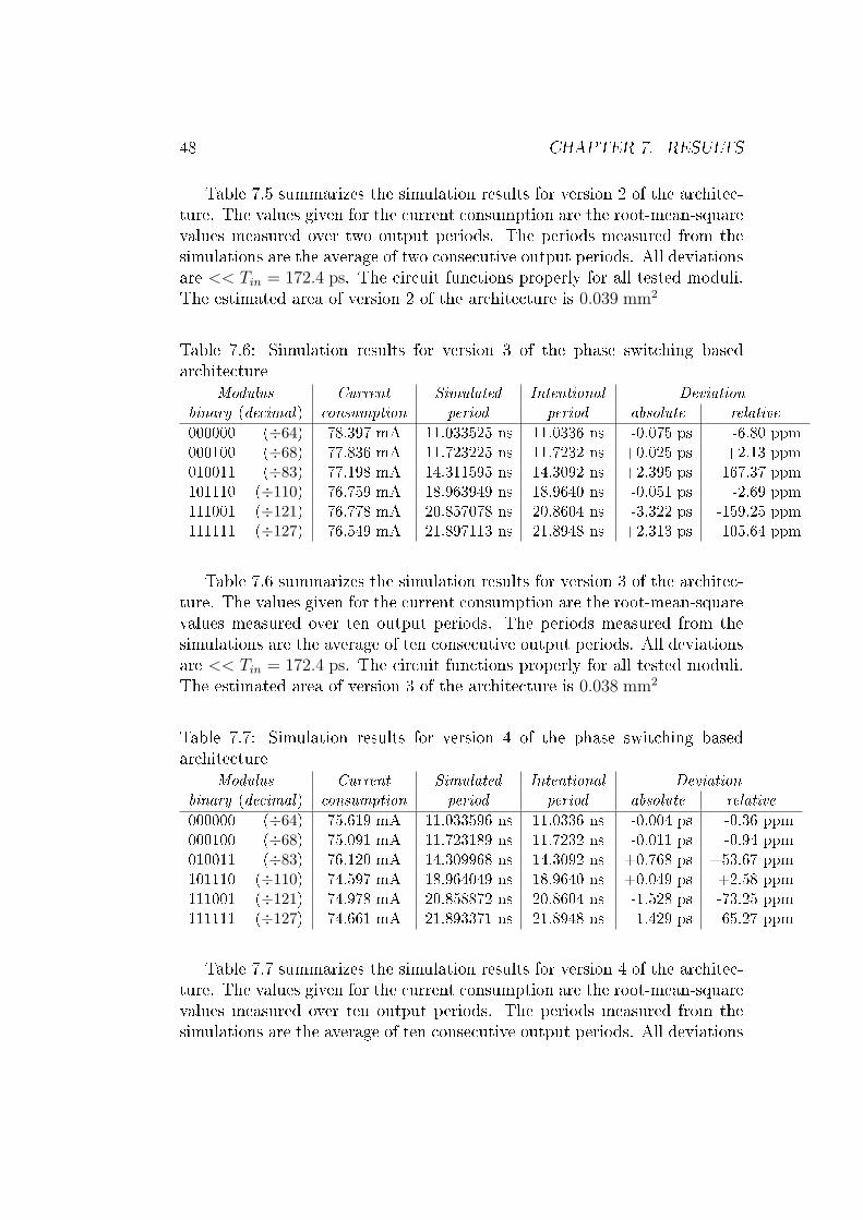
Table 7.6: Simulation results for version 3 of the phase switching basedarchitecture
Modulus Current Simulated Intentional Deviation
binary (decimal) consumption period period absolute relative
000000 (÷64) 78.397 mA 11.033525 ns 11.0336 ns -0.075 ps -6.80 ppm
000100 (÷68) 77.836 mA 11.723225 ns 11.7232 ns +0.025 ps +2.13 ppm
010011 (÷83) 77.198 mA 14.311595 ns 14.3092 ns +2.395 ps +167.37 ppm
101110 (÷110) 76.759 mA 18.963949 ns 18.9640 ns -0.051 ps -2.69 ppm
111001 (÷121) 76.778 mA 20.857078 ns 20.8604 ns -3.322 ps -159.25 ppm
111111 (÷127) 76.549 mA 21.897113 ns 21.8948 ns +2.313 ps +105.64 ppm
Table 7.6 summarizes the simulation results for version 3 of the architec-ture. The values given for the current consumption are the root-mean-squarevalues measured over ten output periods. The periods measured from thesimulations are the average of ten consecutive output periods. All deviationsare << Tin = 172.4 ps. The circuit functions properly for all tested moduli.The estimated area of version 3 of the architecture is 0.038 mm2
Table 7.7: Simulation results for version 4 of the phase switching basedarchitecture
Modulus Current Simulated Intentional Deviation
binary (decimal) consumption period period absolute relative
000000 (÷64) 75.619 mA 11.033596 ns 11.0336 ns -0.004 ps -0.36 ppm
000100 (÷68) 75.091 mA 11.723189 ns 11.7232 ns -0.011 ps -0.94 ppm
010011 (÷83) 76.120 mA 14.309968 ns 14.3092 ns +0.768 ps +53.67 ppm
101110 (÷110) 74.597 mA 18.964049 ns 18.9640 ns +0.049 ps +2.58 ppm
111001 (÷121) 74.978 mA 20.858872 ns 20.8604 ns -1.528 ps -73.25 ppm
111111 (÷127) 74.661 mA 21.893371 ns 21.8948 ns -1.429 ps -65.27 ppm
Table 7.7 summarizes the simulation results for version 4 of the architec-ture. The values given for the current consumption are the root-mean-squarevalues measured over ten output periods. The periods measured from thesimulations are the average of ten consecutive output periods. All deviations

7.3. ARCHITECTURES BASED ON PHASE SWITCHING 49
are << Tin = 172.4 ps. The circuit functions properly for all tested moduli.The estimated area of version 4 of the architecture is 0.036 mm2
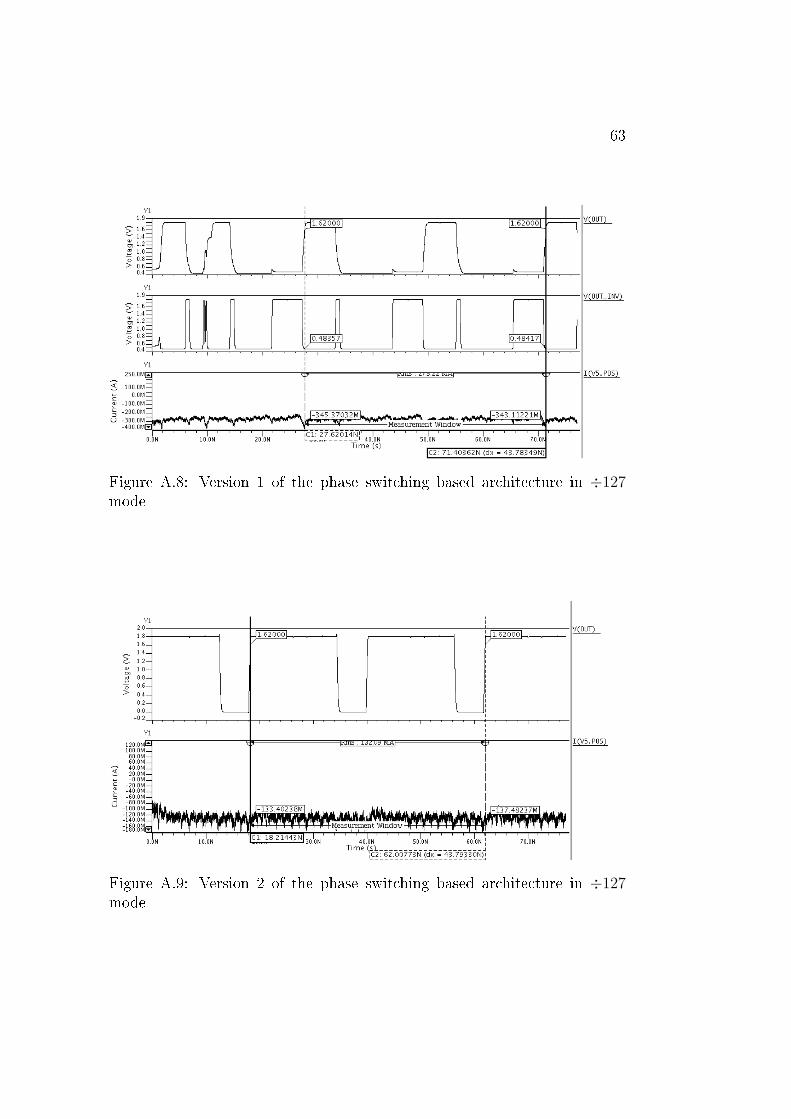
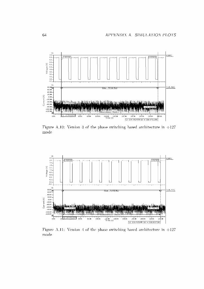
The plots showing each version of the arcitecture in ÷127 mode are shownin �g. A.8 � A.11.

50 CHAPTER 7. RESULTS
Chapter 8
Discussion
8.1 Choice of Architecture
8.1.1 High-Speed Input Divider
Di�erent architectural approaches were tested out. An arcitecture based on÷2/3 cells with local feedback is presented in chapter 3. Two versions of the÷2/3 cell were designed; one using biphase pseudo-NMOS latches, the otherusing standard complementary CMOS latches. Unfortunately none of themwere quick enough to work at the wanted input frequency of the prescaler,5.8 GHz.
An other approach for a high-speed divider to use at the input of theprescaler is the inverter ring divider presented in chapter 4. The initialcircuit that was tested out is a slightly modi�ed version of the one that ispresented in [3]. This ÷4 circuit were implemented in complementary CMOS,and achieved proper operation at 5.2 GHz. However this circuit does not giveout signals in the phases required to be used as inputs to a phase switchingstage. A small adjustment was made to generate the wanted phases. Thisimproved circuit generated output signals in four evenly spaced phases, atan input frequency of 4.5 GHz. Using pseudo-NMOS inverters instead of theCMOS inverters initially used, it generated the wanted phases, at an inputfrequency of 4.8 GHz. The measured current consumptions (see tables 7.1and 7.2) show that the current consumption in the CMOS version increasesrelatively much with frequency, while the current consumption in the pseudo-NMOS version depends less on frequency, as expected. Even at frequenciesas high as 4.5�4.8 GHz it is clear that the pseudo-NMOS version consumesa lot more current than the CMOS version.
In section 5.1 is presented a high-speed divider that works at the requiredfrequency. This is composed of two identical ÷2 circuits, which takes in
51
52 CHAPTER 8. DISCUSSION
two complementary input signals and give out four signals evenly spacedin phase with about 25 % duty cycle. In an input frequency range around5.8 GHz two outputs from the �rst divider are able to drive the second onedirectly, even though these outputs are not exactly complementary. At lowerfrequencies this con�guration causes unwanted spikes at the outputs of thesecond divider. This is explained closer in section 5.1.
The last discussed high-speed divider was a natural choice, as it wasthe only one able to operate at the required frequency. Using pseudo-NMOSinverters in the initial version of the inverter ring divider, in addition to somefurther optimizing, could have made that one run on 5.8 GHz. However itwould still not give out the needed phases, and could not have easily beenused before a phase switching stage.
8.1.2 Phase Switching Stage
Since the input divider only can divide on one modulus, a phase switch-ing stage is a good way to achieve a programmable output signal with theresolution of one period of the input signal.
The phase switching stage is based on the architecture in [2]. It consists ofa four-to-one multiplexer, a phase select state machine and a mapping logiccircuit. The mapping logic circuitry is clocked by the �nal output signal ofthe prescaler, and operates thus on such low frequency that it implementingit in CMOS was a natural choice, with the current consumption in mind.
The phase select state machine and the multiplexer was initially imple-mented in pseudo-NMOS. It was attempted to implement the phase selectstate machine in complementary CMOS, but that attempt failed. The multi-plexer, on the other hand, was easily implemented in complementary CMOS.Simulations showed that implementing the multiplexer in CMOS reduced thecurrent consumption signi�cantly.
8.1.3 Low Frequency Stage
The �rst attempt to implement the low frequency stage was to use the phaseswitcing architecture from [2]. This was implemented in pseudo-NMOS andcontributed considerably to the total current consumption. Converting thiscircuits to complementary CMOS could maybe have been worth the e�ort,and would undoubtly have reduced the current consumption since they arerunning on such relatively low frequencies.
Also two chains of four ÷2/3 cells with local feedback were tried. Thetwo types of ÷2/3 cells are presented in sections 5.4 and 5.6. The latter,based on [1], consumes a little less current, and was therefore chosen.
8.2. IMPLEMENTATION 53
8.2 Implementation
To summarize; the �nal architecture is composed of the four-phase high-speedinput divider presented in section 5.1, the phase select state machine and themapping logic presented in section 5.2, the four-to-one CMOS multiplexerpresented in section 5.5, and four of the ÷2/3 cells presented in section 3.2.
The entire prescaler is implemented using RF transistors models. Thesehave a minimum channel length of 0.18 µm, which is used for all the transis-tors. The minimum channel width is quite large for these transistor models,25 µm. Using other transistor models, allowing smaller channel widths, forthe parts of the circuit that do not operate at the maximum frequency wouldmost likely reduce the current consumption quite a lot.
In addition to the circuits that have been tested, also a complementaryCMOS implementation of the low frequency phase switching stages shouldhave been tried, and an extra e�ort in trying to convert the phase select statemachine in the �rst phase switching stage should have been made. Thosechanges might have improved the prescaler.
8.3 Simulations
The architectures in chapter 5 are simulated for only six di�erent moduli.That is because the simulations are very time demanding. The moduli forwhich they are simulated are however chosen in such a way that they willmost likely detect any errors in functionality
The simulations were done with a di�erential square-wave rail-to-rail in-put signal applied, having a rise/fall time of 10 ps. Having such a signalavailable in a real circuit is not very likely. Generating this signal would behard. Another weakness by the simulations is that parasitic capasitances arenot included. So, even though the circuit operates properly in the simula-tions, it would need further improvements before it could be manufactured.

54 CHAPTER 8. DISCUSSION
Chapter 9
Conclusion
A multi-modulus prescaler, able to divide by any integer modulus in therange 64 to 127, has been designed in a 0.18 µm CMOS process, and worksproperly for a 5.8 GHz input signal, according to simulations.
The �nal architecture is composed of a four-phase high-speed input di-vider, a phase switching stage consisting of a four-to-one multiplexer, a phaseselect state machine and a mapping logic circuit, and four cascaded÷2/3 cellswith local feedback. The high-speed input divider is implemented in pseudo-NMOS to achieve the required speed. The phase select state machine isalso implemented in pseudo-NMOS. The rest of the circuit is implementedin complementary CMOS to minimize current consumption. Complemen-tary CMOS implementations have turned out to be consuming less currentthan pseudo-NMOS implementations for the frequencies of interest. Pseudo-NMOS is however a little faster, and are used only when a proper workingCMOS implementation could not be done.
The prescaler consumes a little more current than intended. In the designan RF transistor model is used, with a minimum channel width of 25 µm.By using other transistor models, allowing smaller channel widths, the cur-rent consumption would probably have been reduced considerably. Anotheritem for further work could be to try to implement the phase select statemachine in complementary CMOS. This circuit is running on one fourth ofthe input frequency, and a CMOS implementation of this would probablyalso contribute to lowering the total current consumption.
55

56 CHAPTER 9. CONCLUSION
Bibliography
[1] Cicero S. Vaucher et al. A Family of Low-Power Truly Modular Program-mable Dividers in Standard 0.35 µm CMOS Technology. IEEE Journal
of Solid-State Circuits, 35(7), July 2000.
[2] Michael H. Perrott. Techniques for high data rate modulation and low
power operation of fractional-N synthesizers. PhD thesis, MassachusettsInstitute of Technology, Sep. 1997.
[3] Carlos E. Saavedra. A Microwave Frequency Divider Using an InverterRing and Transmission Gates. IEEE Microwave and Wireless Compo-
nents Letter, 15(5), May 2005.
[4] A. Mason. Lecture 30: Latches and Flip Flops, ECE 813 Ad-vanced VLSI Design, Michigan State University College of Engineering.http://www.egr.msu.edu/classes/ece813/mason/�les/Lecture30.pdf.
[5] B. Razavi, K. F. Lee and R. H. Yan. Design of High-Speed, Low-PowerFrequency Dividers and Phase-Locked Loops in Deep Submicron CMOS.Journal of Solid State Circuits, 30(2):101�109, Feb. 1995.
57

58 BIBLIOGRAPHY
Appendix A
Simulation Plots
Figure A.1: Simulation plot for ÷2/3 cell with pseudo-NMOS latches atmaximum operation frequency in ÷2 mode
59
60 APPENDIX A. SIMULATION PLOTS
Figure A.2: Simulation plot for ÷2/3 cell with pseudo-NMOS latches atmaximum operation frequency in ÷3 mode
Figure A.3: Simulation plot for ÷2/3 cell with CMOS latches at maximumoperation frequency in ÷2 mode
61
Figure A.4: Simulation plot for ÷2/3 cell with CMOS latches at maximumoperation frequency in ÷3 mode
Figure A.5: Simulation plot for version 1 of the high-speed inverter ringdivider at maximum operation frequency
62 APPENDIX A. SIMULATION PLOTS
Figure A.6: Simulation plot for version 2 of the high-speed inverter ringdivider at maximum operation frequency
Figure A.7: Simulation plot for version 3 of the high-speed inverter ringdivider at maximum operation frequency
63
Figure A.8: Version 1 of the phase switching based architecture in ÷127mode
Figure A.9: Version 2 of the phase switching based architecture in ÷127mode
64 APPENDIX A. SIMULATION PLOTS
Figure A.10: Version 3 of the phase switching based architecture in ÷127mode
Figure A.11: Version 4 of the phase switching based architecture in ÷127mode