Embed Size (px)
Citation preview
A High-speed Inter-process Communication Architecture
for FPGA-based Hardware Acceleration of Molecular
Dynamics
by
Christopher John Comis
A thesis submitted in conformity with the requirementsfor the degree of Master of Applied Science
Graduate Department of Electrical and Computer EngineeringUniversity of Toronto
c© Copyright by Christopher John Comis 2005

ii

A High-speed Inter-process Communication Architecture
for FPGA-based Hardware Acceleration of Molecular
Dynamics
Christopher John Comis
Masters of Applied Science, 2005
Graduate Department of Electrical and Computer Engineering
University of Toronto
Abstract
Molecular dynamics is a computationally intensive technique used in biomolecular simula-
tions. We are building a hardware accelerator using a multiprocessor approach based on
FPGAs. One key feature being leveraged is the availability of multi-gigabit serial transceiver
technology (SERDES) available on the latest FPGAs. Computations can be implemented
by a dedicated hardware element or a processor running software. Communication is imple-
mented with a standard hardware interface abstraction. The actual communication is done
via asynchronous FIFOs, if the communication is on-chip, or via Ethernet and SERDES,
if the communication is between chips. The use of Ethernet is significantly slower than
the SERDES, but allows for prototyping of the architecture using off-the-shelf develop-
ment systems. A reliable, high-speed inter-FPGA communication mechanism using the
SERDES channels has been developed. It allows for the multiplexing of multiple channels
between chips. Bi-directional data-throughput of 1.918Gbps is achieved on a 2.5Gbps link
and compared against existing communication methods.
iii

iv

Acknowledgements
It was with the guidance and support of many people that made the work in this thesis
possible.
Of the many people that have helped me technically, I first and foremost thank my
supervisor, Professor Paul Chow. Without his technical experience and creative approach
to problem solving, my work would have never reached what it is today. I also thank others
in my research group, including Lesley, Chris M., Professor Regis Pomes, Arun, Manuel,
Dave, Sam, Nathalie, Lorne and Patrick for their feedback, guidance and support. I thank
those in EA306, other members of the computer group, and the technical support staff
for their assistance. Thanks go to the organizations that supported this work in its many
forms, including Grants from Micronet and CAD tools and support provided by CMC
Microsystems.
Of those that provided emotional support, above all I thank my Mom, my Dad and
my sister Tracy for their unconditional love, support and encouragement. I also thank the
many great people I’ve met in Toronto that have made the last two years an irreplaceable
chapter of my life. I thank my friends back in Calgary for keeping me posted on the trouble
I’ve been missing out on. I look forward to more great times with all of you in the future.
v

vi

Contents
List of Figures ix
List of Tables xi
1 Introduction 11.1 Motivation and Goals . . . . . . . . . . . . . . . . . . . . . . . . . . . . . . . 11.2 Research Contributions . . . . . . . . . . . . . . . . . . . . . . . . . . . . . . 2
1.2.1 Design of an Effective Run-Time Debug Capability . . . . . . . . . . 21.2.2 Development of a Reliable, High-Speed Communication Interface . . 31.2.3 Design Abstraction . . . . . . . . . . . . . . . . . . . . . . . . . . . . 4
1.3 Thesis Organization . . . . . . . . . . . . . . . . . . . . . . . . . . . . . . . . 4
2 Background 52.1 Overview of Molecular Dynamics . . . . . . . . . . . . . . . . . . . . . . . . 5
2.1.1 Why Molecular Dynamics is Useful . . . . . . . . . . . . . . . . . . . 62.1.2 The Molecular Dynamics Algorithm . . . . . . . . . . . . . . . . . . . 62.1.3 The Complexity of Molecular Dynamics . . . . . . . . . . . . . . . . 9
2.2 Overview of Existing Computational Solutions . . . . . . . . . . . . . . . . . 102.2.1 Hardware Approaches . . . . . . . . . . . . . . . . . . . . . . . . . . 112.2.2 Software Approaches . . . . . . . . . . . . . . . . . . . . . . . . . . . 122.2.3 Alternate Computational Approaches . . . . . . . . . . . . . . . . . . 142.2.4 State-of-the-Art Supercomputing: The IBM BlueGene . . . . . . . . 15
2.3 Overview of Existing Communication Mechanisms . . . . . . . . . . . . . . . 162.3.1 Off-the-Shelf Communication Mechanisms . . . . . . . . . . . . . . . 162.3.2 Custom-Tailored Communication Mechanisms . . . . . . . . . . . . . 192.3.3 Communication Example: The IBM BlueGene . . . . . . . . . . . . . 20
3 System-Level Overview 233.1 An Effective Programming Model for Molecular Dynamics . . . . . . . . . . 233.2 Available Architectures for Data Communication . . . . . . . . . . . . . . . 25
3.2.1 Thread-Based Intra-Processor Communication . . . . . . . . . . . . . 27
vii

Contents
3.2.2 FSL-Based Intra-Chip Communication . . . . . . . . . . . . . . . . . 283.2.3 Ethernet-Based Inter-Chip Communication . . . . . . . . . . . . . . . 283.2.4 SERDES-Based Inter-Chip Communication . . . . . . . . . . . . . . 30
3.3 Producer/Consumer Model Implementation . . . . . . . . . . . . . . . . . . 313.3.1 Run-time Debug Logic: A MicroBlaze-based Debug Environment . . 313.3.2 Logging Debug Logic: Sticky Registers . . . . . . . . . . . . . . . . . 32
4 High-Speed Communication Architecture Implementation 374.1 Architecture Requirements . . . . . . . . . . . . . . . . . . . . . . . . . . . . 374.2 SERDES Fundamentals . . . . . . . . . . . . . . . . . . . . . . . . . . . . . 38
4.2.1 A Simple SERDES Communication Example . . . . . . . . . . . . . . 384.2.2 Practical Issues with SERDES Communication . . . . . . . . . . . . 40
4.3 Xilinx Environment for SERDES Development . . . . . . . . . . . . . . . . . 414.4 Protocol Development . . . . . . . . . . . . . . . . . . . . . . . . . . . . . . 44
4.4.1 Protocol Overview . . . . . . . . . . . . . . . . . . . . . . . . . . . . 444.4.2 Packet Format . . . . . . . . . . . . . . . . . . . . . . . . . . . . . . 464.4.3 Detailed Analysis of a Typical Data Communication . . . . . . . . . 494.4.4 Error Handling . . . . . . . . . . . . . . . . . . . . . . . . . . . . . . 544.4.5 Interface Conflicts and Priority Handling . . . . . . . . . . . . . . . . 56
5 High-Speed Communication Architecture Results 595.1 Design Reliability and Sustainability . . . . . . . . . . . . . . . . . . . . . . 595.2 Throughput and Trip Time Results . . . . . . . . . . . . . . . . . . . . . . . 615.3 Comparison Against Alternate Communication Mechanisms . . . . . . . . . 675.4 Design Area Usage . . . . . . . . . . . . . . . . . . . . . . . . . . . . . . . . 715.5 Evaluation Against Architecture Requirements . . . . . . . . . . . . . . . . . 73
6 A Simple Example: Integration into a Programming Model 756.1 Background on MPI . . . . . . . . . . . . . . . . . . . . . . . . . . . . . . . 756.2 Integration into the MPI-Based Programming Model . . . . . . . . . . . . . 766.3 Software-Based Test Results . . . . . . . . . . . . . . . . . . . . . . . . . . . 77
7 Conclusions and Future Work 81
Appendix 83A Tabulated Throughput and Trip Time Results . . . . . . . . . . . . . . . . . 83
References 87
viii

List of Figures
2.1 An MD Simulation Algorithm . . . . . . . . . . . . . . . . . . . . . . . . . . 7
3.1 MD Simulator Block Diagram . . . . . . . . . . . . . . . . . . . . . . . . . . 243.2 Simple Producer/Consumer Model . . . . . . . . . . . . . . . . . . . . . . . 26
3.3 Thread-Based Intra-Processor Communication . . . . . . . . . . . . . . . . . 283.4 Communication Mechanisms via Standardized FSL Interface . . . . . . . . . 293.5 A Highly Observable/Controllable Run-Time Debugging Environment . . . . 323.6 Sticky Register . . . . . . . . . . . . . . . . . . . . . . . . . . . . . . . . . . 33
3.7 Consumer Sticky Register System-Level Connections (Input Clocks Omitted) 35
4.1 A Simple SERDES Data Transfer Example . . . . . . . . . . . . . . . . . . . 394.2 Virtex-II Pro MGT (from the RocketIO Transceiver User Guide[1]) . . . . . 42
4.3 Communication Using LocalLink and UFC Interfaces . . . . . . . . . . . . . 474.4 Time-Multiplexed Communication to Improve Channel Bandwidth Utilization 484.5 Data Packet Format . . . . . . . . . . . . . . . . . . . . . . . . . . . . . . . 494.6 Acknowledgement Format . . . . . . . . . . . . . . . . . . . . . . . . . . . . 49
4.7 Read and Write to the Transmit Buffer . . . . . . . . . . . . . . . . . . . . . 504.8 Scheduler State Diagram . . . . . . . . . . . . . . . . . . . . . . . . . . . . . 514.9 Read and Write to the Receive Buffer . . . . . . . . . . . . . . . . . . . . . . 544.10 Avoidance of LocalLink and UFC Message Conflicts . . . . . . . . . . . . . . 57
4.11 Avoidance of LocalLink Message and Clock Correction Conflicts . . . . . . . 58
5.1 Test Configuration A . . . . . . . . . . . . . . . . . . . . . . . . . . . . . . . 635.2 Test Configuration B . . . . . . . . . . . . . . . . . . . . . . . . . . . . . . . 63
5.3 Test Configuration C . . . . . . . . . . . . . . . . . . . . . . . . . . . . . . . 645.4 Test Configuration D . . . . . . . . . . . . . . . . . . . . . . . . . . . . . . . 645.5 Data Throughput Results . . . . . . . . . . . . . . . . . . . . . . . . . . . . 655.6 One-Way Trip Time Results . . . . . . . . . . . . . . . . . . . . . . . . . . . 66
5.7 Data Throughput Comparative Results . . . . . . . . . . . . . . . . . . . . . 695.8 Packet Trip Time Comparative Results . . . . . . . . . . . . . . . . . . . . . 705.9 SERDES Logic Hierarchy . . . . . . . . . . . . . . . . . . . . . . . . . . . . 71
ix

List of Figures
6.1 MPI Function Call Example . . . . . . . . . . . . . . . . . . . . . . . . . . . 776.2 MicroBlaze Configurations for Programming Model Integration . . . . . . . . 77
x
List of Tables
1.1 Thesis Contributions . . . . . . . . . . . . . . . . . . . . . . . . . . . . . . . 3
3.1 FSL Function Calls for the MicroBlaze Soft Processor . . . . . . . . . . . . . 27
4.1 Scheduler State Descriptions . . . . . . . . . . . . . . . . . . . . . . . . . . . 524.2 Scheduler State Transition Table . . . . . . . . . . . . . . . . . . . . . . . . 52
5.1 Consumer Data Consumption Rates . . . . . . . . . . . . . . . . . . . . . . . 605.2 128-second Test Error Statistics . . . . . . . . . . . . . . . . . . . . . . . . . 615.3 8-hour Test Statistics . . . . . . . . . . . . . . . . . . . . . . . . . . . . . . . 625.4 Latency in Trip Time of a 1024-byte Packet Transfer . . . . . . . . . . . . . 675.5 Hierarchical Block Description . . . . . . . . . . . . . . . . . . . . . . . . . . 725.6 SERDES Interface Area Statistics . . . . . . . . . . . . . . . . . . . . . . . . 725.7 Debug Logic Area Statistics . . . . . . . . . . . . . . . . . . . . . . . . . . . 73
6.1 Communication Scenarios for Programming Model Integration . . . . . . . . 786.2 Communication Results for Programming Model Integration . . . . . . . . . 796.3 Comparative Results for Programming Model Integration . . . . . . . . . . . 79
Appendix 83A.1 Configuration A and Configuration C Throughput Results . . . . . . . . . . 84A.2 Configuration B and Configuration D Trip-Time Results . . . . . . . . . . . 84A.3 Configuration A Throughput Comparative Results . . . . . . . . . . . . . . . 85A.4 Configuration B Trip-Time Comparative Results . . . . . . . . . . . . . . . . 86
xi

List of Tables
xii

1 Introduction
One of the key areas of research in modern biological science is to understand and predict the
performance of complex molecular building blocks and proteins. Success in this field would
result in better drugs and a better capability to comprehend and control diseases. One
method of achieving this understanding involves synthetically developing complex molecular
structures and analyzing the results in a laboratory environment. Another approach is to
simulate the time-evolution of such molecules using a computationally demanding molecular
modeling technique called molecular dynamics (MD). Many interesting simulations take
months to years on the world’s fastest supercomputers[2].
This introductory chapter elaborates on work presented in this thesis on the development
of a communication infrastructure for molecular dynamics simulations. Section 1.1 will first
provide motivation behind the work presented in this thesis. Section 1.2 will then discuss
significant contributions and Section 1.3 will conclude by discussing the organization of
subsequent chapters.
1.1 Motivation and Goals
The exponential progress of microelectronics has been very apparent in the rapid evolu-
tion of Field Programmable Gate Array (FPGA) technology. This progress has resulted
in several highly attractive advancements. First, more transistors on each FPGA chip en-
ables massive amounts of parallel computation. Second, recent developments of high-speed
input/output transceivers allow data to be transferred at high bandwidths into and out
of FPGAs. As a result, FPGA technology has evolved to the point that computationally
intensive algorithms, such as those involved with molecular dynamics, may be spanned
across several FPGA elements for efficient hardware acceleration.
1

1 Introduction
Realizing this potential, several research groups have attempted FPGA-based MD so-
lutions. However, so far only a few FPGAs have been used to solve this problem. The
Toronto Molecular Dynamics (TMD) machine is an ongoing project in collaboration the
Department of Biochemistry and the Hospital for Sick Children. The primary goal of this
project is to deliver a MD package based upon reconfigurable FPGA technology that is
scalable to hundreds or thousands of FPGAs. A key ingredient to the success of this con-
cept is to effectively relay and communicate data between FPGA processing units. Without
an effective mechanism for communication, the potential of the multiple-processor system
would be significantly degraded.
The generality of existing inter-processor communication protocols introduces overhead
that is unacceptable for the high computational demands of the MD system. For example,
many distributed systems communications protocols introduce unnecessary overhead for
packet collision detection, packet retransmission and network management. As well, many
parallel computing protocols suffer unnecessary overhead due to cache coherence. Because
the multi-processor MD system is fully reconfigurable, a custom protocol may be designed
that introduces minimal overhead. The intent of this thesis is to explore existing com-
munication mechanisms, design a high-speed, low-latency communication mechanism and
develop an abstraction layer for using it.
1.2 Research Contributions
The work involved with this thesis makes several notable research contributions, the most
significant of which being the design of a reliable communication capability across high-
speed serial links. This contribution, as well as others, are summarized in Table 1.1 and
outlined briefly in the sections that follow.
1.2.1 Design of an Effective Run-Time Debug Capability
Prior to development of a communication mechanism, an underlying debug capability is
necessary to assist in the development process and provide several important debug capa-
bilities at run-time. Requirements of this supportive debug infrastructure follow:
2

1.2 Research Contributions
Table 1.1: Thesis Contributions
Contribution Chapter and Section
Run-time Debug Logic Design 3.3High-Speed Interface Design 4.4Design Abstraction 4.4, 6
1. The debug mechanism must provide high controllability and observability into the
design.
2. The debug mechanism must log high-speed data at the rate it is passed through the
system, freeze the captured data when an error has occurred and reproduce the logged
data at a slower system data rate for analysis.
3. The mechanism must be capable of simultaneously debugging multiple FPGAs.
The proposed system-level debug environment to address these requirements is presented
in Section 3.3.
1.2.2 Development of a Reliable, High-Speed Communication
Interface
The primary contribution of this thesis involves the development of a custom communica-
tion interface across high-speed serial links, which takes several basic design criteria into
consideration.
First, the mechanism must deliver packets reliably across a potentially noisy and unre-
liable communication channel. Furthermore, because several high-speed serial links may be
used on each chip, the mechanism must be considerate to area. Because this work is part
of a bigger collaborative project, the underlying details of the communication mechanism
must be abstracted from the user by standard hardware and software interfaces. Finally,
the communication must maintain a reasonable throughput, but more importantly a min-
imal latency in packet communication, herein referred to as one-way trip time. Each of
3
1 Introduction
these considerations were addressed in the high-speed communication development, which
is discussed in further detail in Section 4.4.
1.2.3 Design Abstraction
Because the high-speed communication system is part of a bigger project, two abstraction
layers were developed to hide the implementation details of the high-speed communica-
tion interface. During development of the interface in Section 4.4, a standard hardware
abstraction layer was developed that allows any hardware block to seemlessly connect and
communicate using the high-speed communication interface.
Furthermore, after hardware development and testing were complete, the communica-
tion interface was then incorporated into a layer of software abstraction, where by connect-
ing a processor to the communication interface, communication via the high-speed interface
is achieved through software using a programming model. Development and results of the
incorporation into a software abstraction layer are presented in Chapter 6.
1.3 Thesis Organization
The remainder of this thesis is organized as follows. Chapter 2 first provides brief back-
ground, discusses complexity and the communication requirements of molecular dynamics.
This chapter then discusses different approaches to solving complex problems such as molec-
ular dynamics, and is concluded by a light survey of communication mechanisms. Chapter 3
then discusses several system-level issues. In this chapter, a software programming model
is presented, and the available underlying communication mechanisms to this program-
ming model are discussed. From this programming model, an effective debug environment
for communication development is then derived. Chapter 4 discusses, specifically, the de-
velopment of a high-speed communications capability, the results of which are evaluated
in Chapter 5. Chapter 6 then discusses a simple integration into a software programming
model. Chapter 7 provides conclusions and future work, and Appendix A provides reference
of tabulated data.
4

2 Background
To understand the need for high-speed communication in molecular dynamics, one must
first have a basic understanding of the requirements for molecular dynamics. To begin this
chapter, a brief overview of molecular dynamics will be presented. Following this, the reader
should have a better understanding of the underlying principles of molecular dynamics, as
well as computational requirements for a typical MD simulation. Hence, Section 2.2 will
provide a background on existing architectural solutions to highly-computational problems,
and, where appropriate, will also describe how these solutions have been applied to molec-
ular dynamics. Effective communication is of significant importance to molecular dynamics
simulations. Hence, Section 2.3 will digress slightly, and provide a brief background on the
evolution of data communication to form clusters of processors or chips. Each method of
communication will be compared and trade-offs will be discussed. Where appropriate in
this chapter, the IBM BlueGene[3] will be referenced as an example of a state-of-the-art
solution to high-performance scientific computing.
2.1 Overview of Molecular Dynamics
Because this thesis is focused around MD, the following section will provide a light overview
of molecular dynamics. Section 2.1.1 will provide the reader with some basic MD concepts.
Then Section 2.1.2 will step through a molecular dynamics algorithm, providing a more
detailed analysis of the necessary calculations. Finally, Section 2.1.3 will study, in greater
detail, the complexity of MD. Through a simple example, this section will explain why a
typical desktop computer is insufficient for MD simulations and why alternate architectures
must be explored.
5

2 Background
2.1.1 Why Molecular Dynamics is Useful
Proteins are biological molecules that are essential for structural, mechanical, and chemical
processes in living organisms. During protein synthesis, amino acids are linked together
sequentially, yielding the primary structure of a protein. To fulfill its specific biological
role, this protein must evolve into a highly specific, energetically stable, three-dimensional
conformation through a process known as protein folding.
Previous work has shown that a protein is completely determined by its primary amino
acid sequence[4]. More recent work has also shown that many diseases, such as Alzheimer’s
and Scrapie (Mad Cow) are believed to be a consequence of misfolded proteins[5, 6]. With
these discoveries, tremendous research efforts have been spent on understanding the balance
of biophysical forces responsible for protein folding. Despite the fact that many proteins
fold on a millisecond time-scale, we are still not able to predict the native configuration of
a protein based on its primary amino acid sequence.
Laboratory methods such as X-ray crystallography and Nuclear Magnetic Resonance
imaging are capable of determining structural information. However, these techniques have
limitations which restrict the proteins that can be analyzed. Furthermore, these techniques
generally do not yield information about the protein folding pathway. Computer simula-
tion, on the other hand, can provide atomic-level resolution of the biophysical processes
underlying molecular motion. Molecular dynamics, a computer simulation technique, is a
method for calculating the time-evolution of molecular configurations. This is a promising
approach that is currently being applied to the protein folding problem.
2.1.2 The Molecular Dynamics Algorithm
At this point, the reader will be walked through an algorithm for molecular dynamics simu-
lation. Although there are several MD algorithms, the algorithm presented herein is simple,
and incorporates all the information necessary to understand a typical MD simulation. This
algorithm is summarized in Figure 2.1.
An MD simulation begins by first generating a computer model of a protein of interest.
As indicated in step (1) of Figure 2.1, every atom in the system is assigned initial coordinates
and velocity.
6

2.1 Overview of Molecular Dynamics
(1) Assign Initial
Coordinates and Velocities
(2) Calculate Forces
(3) Calculate New
Coordinates and Velocities
(4) Last Timestep?
(5) Simulation Complete
YES
NO
Figure 2.1: An MD Simulation Algorithm
7

2 Background
The fundamental time increment of the simulation is referred to as a time-step. During
each time-step, the potential energy and resulting net force acting on each atom is calcu-
lated, as indicated in step (2). These potentials are a result of interactions that may be
categorized into two main groups. The first group, bonded interactions, are between atom
pairs that share a covalent bond, and atoms that form geometric angles and torsions. The
potential energy associated with these interactions is calculated in Equation 2.1.
EBondedInteractions =∑
AllBonds
kb (r − r0)2 +
∑
AllAngles
kθ (θ − θ0)2 (2.1)
+∑
AllTorsions
A [1 + cos (nτ + θk)]
Additionally, potential energy must also be calculated for non-bonded interactions. The
van der Waals potential, a measure of the attraction or repulsion between atoms, is mod-
eled through the Lennard-Jones 6-12 equation shown in Equation 2.2. The Electrostatic
potential, a measure of the attraction or repulsion between charged particles, is captured
using Coulomb’s law, shown in Equation 2.3. Unlike bonded interactions, these interactions
can occur between all atom pairs in the simulation.
ELennard−Jones =∑
AllPairs
4ε
[
(σ
r
)12
−(σ
r
)6]
(2.2)
EElectrostatic =∑
AllPairs
q1q2
r(2.3)
For each atom, the potentials from the above equations are summed. The net force
acting on each atom is then determined by taking the negative of the gradient of the
potential energy with respect to the position of the atom. With the net force on each atom
calculated, acceleration may then be determined using Newton’s second law, F = ma.
With the acceleration of each atom determined, time-integration may then be used to
determine updated coordinates and velocities, as shown in step (3) of Figure 2.1. The
8

2.1 Overview of Molecular Dynamics
Velocity Verlet Update (VVU) algorithm may be used for this purpose [7], and the three
equations that must be calculated are given in Equations 2.4, 2.5 and 2.6.
v (t) = v
(
t −δt
2
)
+δt
2× a (t) (2.4)
r (t + δt) = r (t) + δt × v (t) +δt2
2× a (t) (2.5)
v
(
t +δt
2
)
= v (t) +δt
2× a (t) (2.6)
In the above equations, δt is the time-step, r(t + δt) is the updated coordinate position
and v(t+δt/2) is the updated velocity. With updated coordinates and velocities, the current
time-step is concluded. The process is iterated, as calculations are again performed using
the new coordinates and velocities. To simulate biologically relevant time-scales, billions of
time-steps must often be calculated.
2.1.3 The Complexity of Molecular Dynamics
For the purposes of this thesis, a detailed understanding of the above algorithm is not neces-
sary. For more detailed information, the reader is referred to available molecular dynamics
literature [7]. Instead, it is important to understand the computational requirements of
this algorithm. Hence, the complexity of each of the above equations will now be discussed
in more detail.
The calculation of bonded potentials, represented in Equation 2.1 are performed once per
time-step between an atom and its adjacent bonded neighbors. Because this is a calculation
only between atoms of close range, this is an O(n) problem, where n is the number of atoms
in the system. On the other hand, the non-bonded potentials, represented in Equations 2.2
and 2.3, must be calculated between an atom and all other atoms in the system. Although
some optimizations may be applied, this is inherently an O(n2) problem, and the time
9

2 Background
required to solve these potentials is related to the square of the number of atoms in the
system. Finally, the VVU algorithm, represented in Equations 2.4, 2.5, 2.6 must only be
performed on each atom once per time-step. Again, this is an O(n) problem. Clearly,
non-bonded force computations dominate the computational requirements. Previous work
supports this fact. The authors of MODEL[2] find that in an MD simulation involving over
10,000 particles, non-bonded interactions take more than 99% of the total CPU time for
each time-step.
At this point, a simple example will provide more insight into the computational re-
sources required for a typical MD simulation. Because non-bonded force calculations clearly
dominate total CPU time, other computations will be ignored. First assume that an MD
simulation will be performed with a system of 104 atoms. This is a reasonably-sized sys-
tem which may demonstrate interesting biological properties. As the unoptimized calcu-
lation of non-bonded potential is an O(n2) problem, each time-step requires an order of
n2=(104)2=108 computations. A time-step must be of sufficient granularity for an accurate
simulation, and a simulation must run for sufficient time before interesting characteristics
are observed. Hence, a femtosecond will be used as a time-step and the total simulation
time will be a microsecond. If 108 computations are required per time-step, then across 109
time-steps, 108×109=1017 computations are required over the entire simulation. On a typ-
ical desktop computer running at 2GHz, we can generously assume that each computation
takes 2 clock cycles. Hence, a computation is completed every 10−9 seconds. At this rate,
the entire simulation will complete in about 108 seconds, or approximately 3 years.
The above example shows that a desktop computer lacks sufficient computational re-
sources to complete a typical molecular dynamics simulation in a reasonable amount of
time. Alternate computational approaches must be investigated, and are discussed in the
following section.
2.2 Overview of Existing Computational Solutions
Molecular dynamics is a single example of many highly-computational problems. Other
examples include weather prediction and seismic analysis. To overcome these challeng-
ing problems, as well as many others, one may take several possible approaches. These
10

2.2 Overview of Existing Computational Solutions
approaches may be categorized into three main groups. First, Section 2.2.1 describes ded-
icated hardware solutions, where custom hardware is developed targeting the application.
Then, Section 2.2.2 describes software solutions, where, through the use of parallel program-
ming languages and message passing libraries, a software program may span hundreds to
thousands of computers. Finally, Section 2.2.3 describes other computational approaches,
including hybrid solutions and FPGA-based solutions.
2.2.1 Hardware Approaches
For extremely demanding applications, such as those with real-time timing constraints, a
custom application-specific integrated circuit (ASIC) may be designed. Although it requires
considerable effort and cost, there are several advantages to a custom hardware design.
Because the designer may define how transistors are laid out on a chip, by implementing
an algorithm in hardware, a designer may describe the exact data flow through a circuit.
Parallelism may be exploited, and the parallel portion of algorithms may be subdivided
among several identical processing elements. The performance advantages of this approach
are obvious. If an algorithm with O(n2) complexity is equally divided among m processing
elements, then a performance of n2/m may be achieved. Furthermore, in designing a
custom ASIC, highly-demanding design constraints such as a high clock rate, minimal area
or minimal power consumption, may be achieved.
Recent studies have applied custom ASICs to molecular dynamics. In Fukushige et.
al [8], the authors extend the application-space of a previously-developed board, GRAPE,
towards the acceleration of molecular dynamics. All O(n) computations are implemented
on a host computer while all O(n2) Electrostatic and Lennard-Jones computations are
off-loaded to custom ASICs called MD Chips, which each compute forces on six atoms
simultaneously. Multiple versions of the MD-GRAPE board exist[8, 9], the most recent
of which contains eight MD Chips per board, resulting in a 6 gigaFLOPS performance
achievement. The board has since been renamed as ITL-md-one, and has been used in
several MD simulations[10].
In related work, another research group[2] developed a custom board that specifically
targets MD simulation. Similar to the MD-GRAPE, the authors use a host computer to
handle all O(n) computations, and off-load all O(n2) computations to custom hardware
11

2 Background
boards called MD Engines. On each MD Engine are four identical ASICs, called MODEL
chips, each of which is capable of computing a non-bonded interaction every 400ns. Al-
though each MD Engine achieves only 0.3 gigaFLOPS in performance, the system can be
scaled up to 76 parallel cards. Similar to the MD-Grape, this board has again been used as
a speedup mechanism for MD simulations[10].
2.2.2 Software Approaches
Because software is written for a general-purpose architecture, software on a single computer
is not a viable solution to highly-computational problems such as MD. However, with the
improvement of inter-processor communication and the introduction of parallel processing
libraries, a heavy workload may now be distributed across several computers. With respect
to molecular dynamics, the scalability of an implementation method ultimately determines
how effective the program may be used to analyze complex molecules. Two approaches
will be explored, each of which takes a radically different approach to scaling the molecular
dynamics problem.
The Folding@Home project uses an alternate algorithm to that presented in Figure 2.1
to predict the folding of a molecule by determining a series of sequential minimal free-energy
configurations[11]. From the initial molecular configuration, different possible future con-
figurations are constructed, from which the molecular forces and the resulting free-energy
of each configuration is determined. If a new configuration represents a more stable free-
energy minimum, the system is updated with the coordinates of the new configuration and
the process is repeated. Because this algorithm requires minimal communication overhead,
the designers use tens of thousands of personal computers across the Internet as individual
compute nodes. However, there are several limitations to this approach. First, because the
algorithm exhibits an inherent sequential progress between free-energy minimums, scalabil-
ity of the algorithm decreases beyond a certain number of processors[12]. Furthermore, a
folded protein result may not necessarily be thermodynamically meaningful, and in order
to definitely obtain a thermodynamically correct result, the entire free energy landscape
must be explored[13].
Unlike the Folding@Home project, NAMD[14] implements a highly-organized molecular
dynamic simulator where the protein of interest is simulated using the algorithm presented
12

2.2 Overview of Existing Computational Solutions
in Figure 2.1. In a tightly-coupled cluster of processors, NAMD has shown to be effectively
scalable on up to 3000 processors[15], and is recognized as a revolutionary progression in
parallel computing. In NAMD simulations, the computational complexity of MD is reduced
by the two following algorithmic optimizations.
• A cutoff radius is applied to all van der Waals calculations. Atoms separated by a dis-
tance greater than the cutoff value are assumed to experience a negligible interatomic
van der Waals force. This optimization further reduces complexity, as Lennard-Jones
forces no longer need to be calculated between all atom pairs in the system.
• Using the Particle Mesh Ewald algorithm[16], the complexity of electrostatic calcula-
tions may be reduced from O(n2) to O(n×log(n)). To further reduce the computa-
tional overhead, the chosen implementation of this algorithm is parallelizable among
multiple processors.
Further to the above optimizations, the authors of NAMD make several intelligent design
decisions to improve scalability and parallelism.
In the first version of NAMD, the molecular system is partitioned by volume into cubes,
called patches, whose dimensions are slightly larger than the cutoff radius. By implementing
this strategy of spatial decomposition, an atom must only interact with atoms from its local
patch, as well as atoms from its 26 nearest-neighbor patches. This subtle reorganization
of the system results in a fundamental change in scalability. Rather than a divide-and-
conquer approach of using a total of m processors to solve a total of n2 computations,
the problem set is divided per processor. Hence, each processor is responsible for solving
ni2 computations, where ni is the subset of calculations between each atom on the local
patch and all atoms in nearest-neighbor patches. The latter method results in far less
inter-processor communication, and is therefore more effectively scalable among multiple
processors.
The aforementioned method of spatial decomposition has two limitations that inhibit
effective scalability to thousands of processors.
1. The scalability of spatial decomposition is limited by the size of the system being
studied. As an example, using a cutoff radius of 12 angstroms, the 92,000-atom
13

2 Background
ApoA1 benchmark may be divided into only 144 patches[15]. Beyond 144 processors,
the scalability of a patch-based approach is reduced to that of a typical divide-and-
conquer approach, and additional decomposition methods must be considered.
2. A protein under simulation is often submerged in a solvent, where the density of the
solvent is often considerably less than the density of the protein being simulated.
This inherent imbalance in density of patches results in a computational load balance
across the entire system. A more fine-grained decomposition method is necessary.
Because of the above two limitations, another method of decomposition, called force
decomposition, is implemented. In force decomposition, non-bonded force calculations
may be performed on a different processor than the processor where the patch is located.
This finer-grained approach to parallelism overcomes both limitations, resulting in effective
scalability and load balancing on thousands of processors.
2.2.3 Alternate Computational Approaches
The success of FPGA technology in complex computation has resulted in several commercial
products where FPGAs are used as a co-processor alongside traditional desktop processors.
The Annapolis Wildcard[17] is one of the earliest of such products. This card fits in
a standard PCMCIA slot, and is programmed by the user through a C++ application
programming interface (API). Once programmed, the Wildcard then acts as a co-processor
to the host processor. There are currently two versions of the Wildcard, and although the
Wildcard contains only a single FPGA, it has successfully been targeted to a variety of
applications. Results show significant speedup over identical computations where only the
host processor is used[18, 19].
As the capabilities of FPGAs have increased, so has the complexity of the computations
for which they may be used. This has become evident in the integration of FPGAs into sev-
eral high-performance compute servers. Systems by SRC Computers, Inc.[20], for example,
allow several heterogeneous boards to be interconnected along a high-speed communication
interface. For more generic computation, modules called Dense Logic Devices (DLDs) con-
tain general-purpose instruction-set processors. Alternatively, one can also connect Direct
Execution Logic (DEL) modules, which each contain an array of tightly-coupled FPGAs.
14
2.2 Overview of Existing Computational Solutions
These DEL modules handle dedicated hardware acceleration of the most difficult com-
putations, and provide significant speedup over a system containing only general-purpose
processors.
As an alternative to the systems by SRC Computers, Cray has commercialized another
modular system, the Cray XD1 Supercomputer[21]. In this system, a chassis contains
several tightly-coupled general-purpose AMD processors and six tightly-coupled FPGAs.
Similar to the SRC system, the FPGAs are typically devoted to the portions of the algorithm
that are the most computationally-demanding.
Similar to Wildcard, the SRC and Cray compute servers have each demonstrated
effectiveness in a range of computationally-demanding applications, including molecular
dynamics[22]. Results are preliminary, but the authors claim their approach effectively
optimizes molecular dynamics, leading to high performance results.
2.2.4 State-of-the-Art Supercomputing: The IBM BlueGene
The previous three sections described several mechanisms by which supercomputing may
be performed. In this final section, a state-of-the-art supercomputer will be described.
The IBM BlueGene project, initiated in 1999, involves the development of a highly-parallel
supercomputer for scientific computation. Because of its incredible success, the architecture
of the IBM BlueGene will be briefly described here.
The IBM BlueGene supercomputer consists of up to 65,536 nodes arranged in a three-
dimensional torus network. Along with 256MB of SDRAM-DDR memory, each node con-
sists of a single ASIC, consisting of two IBM PowerPC 440 processing cores that have been
enhanced for effective scientific computing. A light-weight low-level kernel allows one to
program the cores with software applications, without introducing significant overhead to
the processor.
Because a system of this magnitude requires significant resources for communication, of
the two PowerPC processors in the system, the first is dedicated solely to scientific compu-
tation, while the second specifically targets message passing. There are five communication
networks in the BlueGene system. These networks will be discussed in further detail in
Section 2.3.3.
With respect to performance, at a target clock rate of 700MHz, each PowerPC processor
15

2 Background
performs at approximately 2.8 gigaFLOPS. Theoretically, if both processors are used for
computation, the BlueGene/L supercomputer may operate at a peak performance of 360
teraFLOPS. However, current measurements using LINPACK[23] target approximately 137
teraFLOPS[24]. At this rate, the IBM BlueGene/L supercomputer is ranked number one
in the 25th Edition of the TOP500 List of World’s Fastest Supercomputers.
2.3 Overview of Existing Communication Mechanisms
Whether an MD system is designed in dedicated hardware, software or by alternate means,
communication overhead is a key factor in determining system performance. Depending
upon system requirements, there are several methods of communication that may be used
to form clusters of processors or chips. Hence, different communication mechanisms will
now be discussed. These methods are best categorized by the degree in which they may be
customized to meet the needs of the application at hand. For less stringent communication
requirements, data communication may be achieved using off-the-shelf components. These
components, which are reviewed in Section 2.3.1, allow the designer to communicate at a
higher level of abstraction using a pre-defined communication protocol. Alternatively, when
developing a custom system with high-performance demands, the designer may choose to
develop an application-specific protocol at a level of abstraction much closer to the raw
physical media. These low-level communication mechanisms, which allow the designer to
more aggressively tailor the protocol to the demands of their application, are described in
Section 2.3.2.
2.3.1 Off-the-Shelf Communication Mechanisms
When a means of data communication is necessary, there are several off-the-shelf compo-
nents that may be used. Because these components adhere to a pre-determined specifica-
tion, using them as a mechanism of relaying information requires little development work.
Examples of such components are briefly summarized below.
• Serial RS-232
16

2.3 Overview of Existing Communication Mechanisms
One of the earliest methods of digital data communication is through a serial link,
using the RS-232 standard. This standard specifies signal voltages, signal timing,
signal functions, a protocol for information exchange, and mechanical connections.
Although RS-232 provideds a standardized means of communication, its technology
is obsolete. With a peak throughput of only 120kbps, alternate means offer improved
error control and throughput.
• Ethernet (10/100/1000)
Ethernet parts are a commodity on every FPGA development board. They are read-
ily available and cheap. Although Ethernet is universally used for message passing
communications, there are several disadvantages to using Ethernet for high-speed
communication.
Standardized communication with other Ethernet devices typically involves using
one of several pre-defined protocols, the most common of which being TCP/IP or
UDP/IP. These protocols, although convenient, consist of several layers, all of which
must be implemented and subsequently traversed for each data transaction. Hard-
ware implementation of the protocol stack is costly. Therefore, the protocol stack is
most commonly implemented in software. This has detrimental effects to the overall
trip time of the packet, adding significant overhead. Although this overhead is largely
dependent on the speed of the processor traversing the protocol stack, previous work
shows that protocol software overheads are very high. During the time spent travers-
ing the protocol for a round-trip transfer of data, between 100,000 and 150,000 integer
instructions could have been implemented[25].
In addition to overhead with respect to trip time, traversing the protocol stack also
results in considerable overhead in the packet size, as a header is added at each pro-
tocol layer. As an example, a message being passed via TCP/IP would have 56 bytes
augmented (transport: 20, network: 20, data link: 16)[26], not including contribu-
tions from the application layer. This overhead is considerable for an MD system
similar to NAMD, where the fundamental data unit communicated in the system is
less than 200 bytes[27].
• Other Standardized Communication Protocols
17

2 Background
The need for effective communication in a variety of different scenarios has led to
the introduction of many other standardized communication protocols. The shear
number of available specifications makes it impossible to discuss each specification in
detail. Instead, three categories of specifications will be discussed and examples from
each will be provided. Because of its relevance to this thesis, the third category of
high-speed point-to-point links will be discussed in greater detail.
1. System Area Network (SAN) Protocols
A SAN is used to cluster systems together to form larger, higher available sys-
tems, within a range of approximately 30 meters. Operations through SAN
systems are typically abstracted through software, using either a message pass-
ing interface or a shared memory abstraction. Examples of protocols targeting
such systems include Infiniband, iSCSI and various Fibre-channel protocols[28].
2. Multi-Drop Shared Bus Interfaces
A multi-drop shared bus is typically the backbone to a single computing plat-
form. In such systems, several devices multiplex data, address and control lines,
and communication between devices is performed using a shared memory map.
Examples of protocols for such an environment include PCI, PCI-X, SysAD and
AGP8X[29, 30].
3. High-Speed Point-to-Point Protocols
Although a shared bus is central to most computing systems, a shared bus typi-
cally delivers insufficient bandwidth for a subset of the communication in modern
stand-alone computing systems. To overcome this limitation, several high-speed
point-to-point protocols have been developed for high-bandwidth communication
between devices. Hypertransport is one such protocol, where packet-oriented
data is communicated in parallel along with an explicit clock signal. Although
having several parallel lines may complicate board-level routing, such a parallel
system is light-weight, delivers low-latency, and allows for simple implementa-
tion. Competing with Hypertransport are several protocols that deliver data
serially. By encoding the serial data appropriately, the clock may be recovered
from the serial data stream, and no explicit clock signal is necessary. Having only
18

2.3 Overview of Existing Communication Mechanisms
a single high-speed serial signal eases board level routing and allows more point-
to-point serial links. However, the overhead associated with framing, channel
coding and clock recovery results in increased latency for each packet transfer.
Examples of such serial protocols include RapidIO and PCI-Express. These two
protocols are very similar, with only two notable differences. First, unlike PCI-
Express, the RapidIO protocol allows four prioritized in-band channels through
the same serial channel. Second, RapidIO requires an explicit acknowledgment
for every packet sent, while PCI-Express allows for an acknowledgement after a
sequence of packets[29, 31].
2.3.2 Custom-Tailored Communication Mechanisms
As previously mentioned, when designing a custom system with stringent communication
requirements, the designer may choose to implement a custom communication protocol
to better meet the communication requirements. In such a system, there are two main
methods of inter-chip communication. First, data may be sent in parallel using a wide
parallel bus. Second, data may be sent via a high-speed serial link. The trade-offs of these
two methods are analyzed below.
• Wide-Bus Chip-to-Chip Communication
In a system where low-latency, high-throughput is required between a small number
of chips, the designer may develop a communication protocol using a wide parallel
data bus. Because an explicit clock is sent in a dedicated wire, implementation is
straight-forward. Although this offers minimal latency in data transfer, the demand-
ing requirements of routing at the board-level severely limits the number of point-to-
point connections. Hence, in a multi-chip system where each chip must communicate
with many other chips, significant latency may be introduced as a data packet may
traverse through several chips before reaching its destination.
• High-Speed Serial Communication
As an alternative to wide-bus communication, recent advancements in serial/deserializer
(SERDES) technology allow high-speed data transfers via a serial link. Although sig-
nificant latency may be introduced by framing, encoding and clock recovery, the
19

2 Background
board-level routing of such a communication system allows many point-to-point con-
nections. In a multi-chip reconfigurable system with high communication require-
ments, a simple protocol developed around high-speed serial links offers an effective
method for high-speed chip-to-chip communication.
2.3.3 Communication Example: The IBM BlueGene
As previously mentioned, the IBM BlueGene is an excellent modern example of a high-
performance scientific computing architecture. To conclude the exploration of communi-
cation architectures and protocols, the network architecture of the BlueGene will now be
discussed, and significant communication protocol and architectural design decisions will
be reviewed.
The IBM BlueGene communication architecture consists of five networks between nodes:
1. a 3D torus network for point-to-point message passing
2. a global combining/broadcast tree
3. a global barrier and interrupt network
4. a Gigabit Ethernet to JTAG network
5. a Gigabit Ethernet network for connection to other systems
Several of these networks may be combined to implement a single message transfer. For
example, a compute node interacting with the Gigabit Ethernet network (5) must first send
a message through the global combining/broadcast tree (3) to a special I/O node. This
I/O node, in turn, relays the message outward.
Although all of these networks are necessary for overall system operation, networks 2
through 5 have a secondary role in the communication for scientific computation. Therefore,
the first network, a point-to-point 3D torus network, will now be analyzed in more detail.
A 3D torus network consists of a 3D mesh, where each outside node is connected to
the node on the opposite side of the mesh. The result is a system where every node has
six nearest-neighbor connections. The nearest-neighbor connections implement a custom
protocol using high-speed SERDES links targeting 175MB/s performance. The links are
20

2.3 Overview of Existing Communication Mechanisms
managed by custom embedded routers, which, in turn, are managed by a dedicated Pow-
erPC processor on each node.
Packets range from 32 bytes to 256 bytes in size, and several packets may be combined
for each message. Packet throughput is significantly increased by the use of four Virtual
Channels (VCs). While two virtual channels are statically routed, the majority of traffic is
expected to route through the remaining two dynamic VCs. Preliminary implementation of
an all-to-all broadcast across the torus network suggests that the addition of two dynamic
VCs increases average link utilization from 76% to 99%[3].
With respect to the high-speed SERDES protocol, six “hint” bits are added to the
header of each packet[32]. These bits provide preliminary information to the direction that
a packet must be routed, allowing efficient pipelining of the arbitration process. A 24-byte
CRC is augmented to the end of each packet, and an 8-byte acknowledge is sent for each
successful packet transmission.
For further details about the communication architecture of the IBM BlueGene, the
reader is referred to the IBM BlueGene website[33].
21

2 Background
22

3 System-Level Overview
Prior to discussing the development of a communications protocol, this chapter will first
derive the system-level architecture in which the communication mechanism will be used.
In Section 3.1, our first approach to an MD simulator will be introduced, and NAMD will be
referenced as a starting point from which a programming model will be developed for this
system. Section 3.2 will then isolate the communication portion of this programming model,
and an equivalent basic producer/consumer model will be introduced. Several different com-
munication mechanisms for the producer/consumer model will be discussed. Finally, this
chapter will conclude by describing an implementation of the producer/consumer model.
Because this model would be eventually used in communication protocol development,
strong consideration was given toward an effective method of debugging and verification.
Therefore, the final section of this chapter will discuss the implementation of this simplified
producer/consumer model, paying particular detail to debugging and verification strategies.
3.1 An Effective Programming Model for Molecular
Dynamics
Using modern Xilinx embedded development tools, an FPGA may be populated with one or
more processor cores, called MicroBlaze processors[34]. Each processor core may be synthe-
sized onto the FPGA fabric. Software code may be written for each MicroBlaze core and the
code for each core may be compiled and concurrently executed. Rather than immediately
targeting hardware, our first step in building an MD simulator on reconfigurable logic is to
implement it in software, spanning several of these processors. Ongoing work in our group
involves an object-oriented model for this initial software-based MD simulator, a block dia-
23

3 System-Level Overview
Figure 3.1: MD Simulator Block Diagram
gram of which is shown in Figure 3.1[27]. In this diagram, blocks represent computational
objects, while arrows indicate communication between two computation blocks.
Although this first implementation will be sub-optimal with respect to performance, it
provides an initial proof of correctness, allows an easier debugging environment, and allows
experimentation with different control structures. After the initial software implementation
is complete, dedicated hardware blocks may replace the generic software-driven processors,
and significant speedup may then be obtained.
As previously mentioned, NAMD is regarded as an MD simulator that may be effectively
parallelized across thousands of processors. Because of this, it is reasonable to suggest that
NAMD may be used as a starting point in determining an effective programming model for
the proposed MD simulator.
24

3.2 Available Architectures for Data Communication
Further analysis of NAMD’s programming structure reveals the following:
1. Force calculations (bonded and non-bonded) are programmed as compute objects. A
compute object is necessary for each calculation, and all compute objects are launched
upon program initialization.
2. Message passing of forces and atomic coordinates is also achieved through independent
communication objects. Using a mailbox system, a suspended message-passing object
is awoken when it has received all information to be sent. At this point, data is sent
via a socket. Following data transmission, the message-passing object is again put to
sleep.
In a first object-oriented implementation of the block diagram in Figure 3.1, a program-
ming model similar to that of NAMD will be used. There will be two base classes of threads.
The first base class, computation threads, will be used for all force computations, as well
as all other calculations as indicated in Figure 3.1. The second base class, communication
threads, will be used for all message passing in the system as again indicated in Figure 3.1.
Completion of the MD simulator in Figure 3.1 is not necessary for the purposes of
this thesis. However, in implementing inter-chip communication, the aforementioned pro-
gramming model of computation and communication threads must be considered. Any
communication mechanism must be incorporable into this model.
3.2 Available Architectures for Data Communication
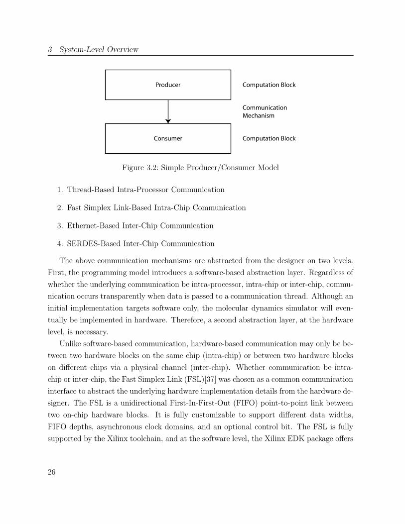
From the communication standpoint, we may now generalize the block diagram of Figure 3.1
into a simpler producer/consumer model, as shown in Figure 3.2. In this simplified diagram,
both the producer and the consumer blocks represent computation threads, and the arrow
between these two blocks represents a means of communication.
Section 2.3.2 provides a summary of currently available communication mechanisms.
However, given the limitations of the available hardware resources[35, 36], we are limited
to four mechanisms of communication that are listed here and explained in further detail
below:
25
3 System-Level Overview
Producer
Consumer
Computation Block
Computation Block
Communication
Mechanism
Figure 3.2: Simple Producer/Consumer Model
1. Thread-Based Intra-Processor Communication
2. Fast Simplex Link-Based Intra-Chip Communication
3. Ethernet-Based Inter-Chip Communication
4. SERDES-Based Inter-Chip Communication
The above communication mechanisms are abstracted from the designer on two levels.
First, the programming model introduces a software-based abstraction layer. Regardless of
whether the underlying communication be intra-processor, intra-chip or inter-chip, commu-
nication occurs transparently when data is passed to a communication thread. Although an
initial implementation targets software only, the molecular dynamics simulator will even-
tually be implemented in hardware. Therefore, a second abstraction layer, at the hardware
level, is necessary.
Unlike software-based communication, hardware-based communication may only be be-
tween two hardware blocks on the same chip (intra-chip) or between two hardware blocks
on different chips via a physical channel (inter-chip). Whether communication be intra-
chip or inter-chip, the Fast Simplex Link (FSL)[37] was chosen as a common communication
interface to abstract the underlying hardware implementation details from the hardware de-
signer. The FSL is a unidirectional First-In-First-Out (FIFO) point-to-point link between
two on-chip hardware blocks. It is fully customizable to support different data widths,
FIFO depths, asynchronous clock domains, and an optional control bit. The FSL is fully
supported by the Xilinx toolchain, and at the software level, the Xilinx EDK package offers
26

3.2 Available Architectures for Data Communication
Table 3.1: FSL Function Calls for the MicroBlaze Soft Processor
C Function CallAssembly-Level
DescriptionInstruction
microblaze bread datafsl(val, id) get blocking data readmicroblaze bwrite datafsl(val, id) put blocking data writemicroblaze nbread datafsl(val, id) nget non-blocking data readmicroblaze nbwrite datafsl(val, id) nput non-blocking data writemicroblaze bread cntlfsl(val, id) cget blocking control readmicroblaze bwrite cntlfsl(val, id) cput blocking control writemicroblaze nbread cntlfsl(val, id) ncget non-blocking control readmicroblaze nbwrite cntlfsl(val, id) ncput non-blocking control write
support for FSL reads and writes with MicroBlaze processors via eight C function calls that
map to assembly-level instructions. A summary of these calls is found in Table 3.1.
Each of the four communication mechanism are described below, and further details are
provided on how each communication mechanism is abstracted.
3.2.1 Thread-Based Intra-Processor Communication
When a producer thread on one processor must communicate with a consumer thread on
the same processor, communication is trivial and no specific underlying hardware commu-
nication mechanism is required. Two communication threads are launched as an interme-
diary between the two computation threads. When data must be sent from the producer
computation thread, the data is placed in a queue that is shared between the producer
computation thread and the producer communication thread. When this data is ready
to be sent, the producer communication thread establishes a socket connection with the
equivalent thread at the consumer as a means of shared-memory data transfer between
the two threads. Data is then passed from the producer to the consumer via socket data
transfers. The process is reflected at the consumer. Once data is received via the socket
connection, it is again placed into a queue by the consumer communication thread for use
by the consumer computation thread. A diagram of this scenario is shown in Figure 3.3.
27

3 System-Level Overview
Producer Consumer
Communication
Thread
Message
Queue
Computation
Thread
Communication
Thread
Message
Queue
Computation
Thread
Socket
Figure 3.3: Thread-Based Intra-Processor Communication
3.2.2 FSL-Based Intra-Chip Communication
When a producer thread must communicate with a consumer thread on a different processor
on the same FPGA, the chosen means of intra-chip communication is via a dedicated Fast
Simplex Link (FSL) connection between the two processors. As before, on the producer
processor, a producer communication thread is launched as an intermediary between the
computation thread and its communication partner. In support of the programming model,
data is first placed in a shared queue between the computation thread and the communi-
cation thread. However, rather than communication via sockets, data is then passed to the
FSL via the FSL write calls described in Table 3.1.
This process is reflected on the consumer processor. Data is received by the communi-
cation thread with the FSL read function calls. Through a shared queue connection, the
data is then passed from the communication thread to the consumer computation thread.
A diagram of a simple FSL link is shown in Figure 3.4(a).
3.2.3 Ethernet-Based Inter-Chip Communication
Because it is readily available in our environment on our development boards, Ethernet
is a convenient means for inter-chip communication. For Ethernet-based communication,
the interaction between threads is identical to the FSL-based intra-chip implementation,
28

3.2 Available Architectures for Data Communication
Producer Consumer....
FSL
FPGA x
(a) FSL-Based Intra-Chip Com-munication
Shared Ethernet Bus
....
MicroBlaze
FS
L
Producer
Ethernet Interface
....
MicroBlaze
FS
L
Consumer
Ethernet Interface
....
MicroBlaze
FS
L
Consumer
Ethernet Interface
....
MicroBlaze
FS
L
Consumer
Ethernet Interface
....
FS
L
Producer
FPGA w FPGA x FPGA y FPGA z
(b) Ethernet-Based Inter-Chip Communication
Bidirectional SERDES Link
....
FS
L
Consumer
FS
L
Producer
SERDES Interface
.... ....
FS
L
Consumer
FS
L
Producer
SERDES Interface
....
FPGA x FPGA y
(c) Simple SERDES-Based Inter-Chip Communication
Figure 3.4: Communication Mechanisms via Standardized FSL Interface
29

3 System-Level Overview
in that from the communication thread, the same FSL read and write calls are used. How-
ever, because data must now be relayed off chip, additional hardware support is necessary.
Previous work implements a simplified Ethernet protocol stack in software[38]. Although
costly, a dedicated Ethernet MicroBlaze may be combined with a dedicated Ethernet hard-
ware interface for Ethernet-based communication. In relaying data between the producer
MicroBlaze and the Ethernet MicroBlaze, as well as the Ethernet MicroBlaze and the Con-
sumer MicroBlaze, the FSL was again used to maintain a consistent hardware abstraction
interface. Because Ethernet communication occurs over a shared bus, several producers
and consumers may communicate along a shared Ethernet link. Figure 3.4(b) shows an
example Ethernet configuration, including a producer chip w, two consumer chips x and y,
and chip z, which acts as both a consumer and a producer. Each producer and consumer
communicates via FSL to a MicroBlaze processor that implements the simplified Ethernet
protocol stack. Data is communicated between the MicroBlaze and the Ethernet physical
media via an additional dedicated hardware Ethernet Interface.
3.2.4 SERDES-Based Inter-Chip Communication
Finally, because Xilinx includes dedicated SERDES hardware in several FPGA families,
SERDES is a viable means of high-speed data communication. Unlike Ethernet-based
communication that usually requires complex protocols to be implemented in software, the
high throughput rate of SERDES links necessitates dedicated hardware logic for communi-
cation. In support of a software abstraction interface, the threading structure within each
MicroBlaze is identical to the two previous implementations. Furthermore, in support of a
standard hardware interface, an FSL link will again be used.
Figure 3.4(c) shows a basic bi-directional SERDES configuration, where data is first
communicated from a producer to a SERDES interface block via FSL, then sent off-chip
via a point-to-point SERDES link. Data is then received by the SERDES interface, and an
FSL is again used to communicate data to the respective consumer. The development of
a SERDES interface is the primary focus of this thesis. Section 3.3 will next describe how
producers and consumers were implemented prior to the interface development.
30

3.3 Producer/Consumer Model Implementation
3.3 Producer/Consumer Model Implementation
Although a specific thread-based programming model is targeted for implementation of the
MD simulator, test vectors and verification logic should not be coded in software. Because
the throughput of software is considerably slower than an equivalent hardware solution,
many potential bugs and corner conditions may be found in hardware that may not be
found in software.
As a result, producer and consumer hardware blocks were created for communications
development. Then, as discussed in Chapter 6, once a reliable communication mechanism
was developed, it was incorporated back into the programming model.
In designing logic surrounding the communication mechanism, there are two key factors
that are important for effective verification and debugging:
1. A high degree of real-time observability and controllability in the design.
2. A means of logging previously-processed data so that when an error occurs in the
design, this logged data may be analyzed to pinpoint the source of the error.
The solutions to the above two challenges are discussed in Sections 3.3.1 and 3.3.2.
3.3.1 Run-time Debug Logic: A MicroBlaze-based Debug
Environment
In Section 3.2, it was determined that an FSL link will act as a connection between the
producers, consumers and SERDES logic. As an alternative to an FSL, there is another
standardized means of communication for a MicroBlaze on an FPGA: the On-Chip Pe-
ripheral Bus (OPB)[39]. The OPB is a bus interface that allows standardized intellectual
property (IP) cores, such as a MicroBlaze, a timer, an interrupt controller and a Universal
Asynchronous Receiver/Transmitter (UART) to be seamlessly dropped into a shared bus
interface, as shown in Figure 3.5(a). Although the OPB is disadvantageous for timing-
critical processing, it is a useful means for reading from and writing to other blocks in the
system.
An OPB was used in the development of a high-speed SERDES communication mecha-
nism. The SERDES logic acts as a slave on the OPB, and a set of 27 32-bit address-mapped
31

3 System-Level Overview
MicroBlazeInterrupt
Controller
UARTTimer
TX/RX
OPB
(a) A Simple Example OPB Config-uration
SERDES Link
Producer
Consumer
....
....
FS
L FS
L
HW
MicroBlazeInterrupt
Controller
UARTTimer
TX/RX
OPB
(b) An OPB-Based Debug Environment
Figure 3.5: A Highly Observable/Controllable Run-Time Debugging Environment
registers are accessible by a MicroBlaze acting as a Master on the OPB. Through these reg-
isters, the SERDES logic may be observed and controlled using software at run-time. In
addition, the producers and consumers also sit as slaves on the OPB, allowing register
access to all blocks involved in data communication. A diagram of the OPB test system
configuration is shown in Figure 3.5(b).
3.3.2 Logging Debug Logic: Sticky Registers
There is a limitation to the OPB logic presented in Section 3.3.1. Although this OPB logic
is useful for monitoring and controlling system status, there are several reasons why the
32

3.3 Producer/Consumer Model Implementation
...
data_out
enable
data_in
enable
clock_b clock_a
FIFO almost full?yes
sticky_freeze_in
serdes_clock_in
synchronizer
sticky_read_in
sticky_data_out
opb_clock_in
FIF
O sticky_data_in
FIFO empty? sticky_empty_out
Figure 3.6: Sticky Register
Microblaze is insufficient to keep track of all data that is processed and passed through
the high-speed links. First, a single functional line of C code often requires several clock
cycles to be implemented. Furthermore, several lines of C code are necessary to process
high-speed data. Because of these inherent limitations in the Microblaze processor, an
additional means of debugging is necessary.
A sticky register is essentially a 32-bit wide, 1024-word deep FIFO that is clocked at
the same rate as data passing through the SERDES (Figure 3.6). Various signals and
register values may be used as FIFO inputs (sticky data in). As the system continues
to process data, the inputs are continually clocked into the head of the FIFO. To prevent
FIFO overflow, simple logic detects when the FIFO is approaching capacity, at which point
data is pulled from the tail of the FIFO.
When an obvious error has occurred in the system, the sticky freeze in signal is
registered high, at which point the FIFO freezes and data is no longer clocked into the head
of the FIFO. Each sticky freeze in signal is also mapped as a bit in the OPB register
map described in Section 3.3.1. Hence, by continually monitoring the sticky freeze in
signal using the OPB, when an error does occur, data may be re-clocked to the OPB clock
using a synchronizer, and the MicroBlaze may then pull data from the tail of the FIFO at
a slower data rate. A FIFO empty signal indicates to the Microblaze that all FIFO data
33

3 System-Level Overview
has been taken. The Microblaze is programmed to then bitmask, rearrange, and print the
logged FIFO data to a UART that resides on the OPB. By connecting the UART to a host
PC, the data is then captured in a terminal window and copied into a spreadsheet. By
analyzing the logged data in a spreadsheet, the source of the error may be determined.
To sufficiently pinpoint and diagnose errors, several sticky registers are necessary, and
as an example, Figure 3.7 illustrates how the sticky register at a consumer communicates
to the rest of the system. Because all sticky registers must immediately halt when an error
is detected, the sticky freeze out signal forwards the current freeze conditions to all
other sticky registers, and the sticky freeze in signal is the bitwise-OR of the sticky
freeze conditions from all other sticky registers in the system. Furthermore, as shown in
Figure 3.7, several signals are mapped to OPB registers. The sticky freeze out signal
indicates to the Microblaze that an error has occurred and the system state has been frozen.
From the Microblaze, the sticky read in signal pulls data from the head of the FIFO.
The raw sticky data (sticky data out) is given a unique register address on the OPB,
and the sticky empty signal indicates that all data has been read from the FIFO. In
addition to a sticky register at each consumer, five sticky register are nested in the SERDES
interface logic (two in the transmitter and three in the receiver). These remaining sticky
registers are networked at the system level in an identical fashion to the sticky register
found in each consumer.
There are several advantages to this debug approach. First, the sticky register system
works well within the existing OPB system, as sticky registers map logically to the existing
OPB register interface. Also, because there is an excess of chip real-estate, there is no
penalty in using the sticky registers during development. Furthermore, although Xilinx
Chipscope Pro[40] provides a run-time debugging interface that may accomplish similar
results, Chipscope supports debugging through JTAG interface. This is insufficient because
only one JTAG interface is available, but an inter-chip communication problem must be
diagnosed concurrently on two separate boards. Finally, sticky registers are simple and
easily modifiable.
34

3.3 Producer/Consumer Model Implementation
Mapped to
OPB Interface
Sticky
Freeze
Conditions
Sticky
RegisterTo all other sticky registers
From all other
sticky registers sticky_freeze_in
sticky_empty
sticky_data_out
sticky_freeze_out
Re
gis
ters
sti
cky_
da
ta_
in
sticky_read
Figure 3.7: Consumer Sticky Register System-Level Connections (Input Clocks Omitted)
35

3 System-Level Overview
36

4 High-Speed Communication Architecture
Implementation
Previous chapters describe the motivation for high-speed communication in molecular dy-
namics and briefly describe SERDES as a possible means to achieve this capability. The
majority of the work in this thesis involved the development of a reliable, light-weight
communication mechanism using SERDES that are available on Xilinx Virtex-II Pro and
Virtex-II Pro X FPGA families. The following sections will describe this implementation.
In Section 4.1, the requirements for the SERDES implementation will be formalized.
Then Section 4.2 will describe the fundamental considerations necessary to achieve SERDES
communication. Section 4.3 will then describe the Xilinx environment that is available
for designing an FPGA-based SERDES capability. Section 4.4 concludes this chapter by
describing underlying implementation details. A protocol overview is provided and the
chosen packet format is discussed. The reader is then walked through an example packet
transmission. This section is concluded by discussing methods of error detection and the
priorities that were necessary to avoid conflicts between different messages in the system.
4.1 Architecture Requirements
Although lightly touched upon in previous chapters, the requirements for an inter-chip data
transfer across SERDES links will be formally discussed. These requirements have driven
development decisions, and will be used as evaluation criteria in subsequent chapters.
1. Reliability
The protocol must react and recover from all possible combinations of data errors,
37
4 High-Speed Communication Architecture Implementation
channel errors and channel failures. From the perspective of someone using the
SERDES interface, any transfer must be reliable and error-free.
2. Low Area Consumption
Because several SERDES links will be used on each FPGA, area consumption for
communication across each SERDES link must be minimized.
3. Minimal Trip Time
The majority of data being transferred around the system is atomic information,
consisting of an identifier, X, Y and Z coordinates[27]. The delay associated with
the transfer of atomic data propagates to a delay in subsequent force calculations.
Because of this, a minimal trip time is necessary in data communication.
4. Abstraction
As described in Section 3.2, the architecture must be abstracted at two levels. First,
the design must be incorporable into the programming model described in Section 3.1.
Second, any communication to the interface at the hardware level must be via a
standardized FSL protocol.
The above criteria were critical in designing a SERDES capability for molecular dynamics.
In Chapter 5, these criteria will be revisited and used in an evaluation of the overall design.
4.2 SERDES Fundamentals
The design of a protocol using SERDES links should not be explained until the under-
lying concepts of SERDES communication are discussed. This section will first provide
a basic SERDES communication example. Several practical problems regarding SERDES
communication will then be discussed, as well as the tools that are used to overcome them.
4.2.1 A Simple SERDES Communication Example
A SERDES data communication starts at the transmitter, where a data word is passed to
a dedicated SERDES engine. The engine then serializes the data word into a single 1-bit
38

4.2 SERDES Fundamentals
clock
multiplier
CDR
engine
32:1
mux
1:32
demux
parallel clock
serial clock =
32 x parallel clock
parallel data
32 bits
serial data
Transmitter
phase
align
engine1 bit
parallel data
32 bits
receiver parallel clock
Receiver
serial clock
Figure 4.1: A Simple SERDES Data Transfer Example
serial stream at a bit rate equivalent to the product of the data word clock rate and the
width of the data word. For example, if a data word of width 32-bits is passed into the
SERDES engine at a rate of 50MHz, the resulting 1-bit serial stream is clocked at a bit
rate of 32 × 50MHz = 1.6Gbps. The 1-bit stream may then be encoded, adding further
overhead. For example, 8B/10B encoding (discussed in Section 4.2.2) adds 25% overhead,
resulting in a 2.0Gbps bit rate. The high-speed serial stream is then transmitted across the
communications medium.
At the receiving end, the high-speed serial data is received by a reciprocal deserializing
engine. Although the receiver may have its own clock, this clock is not in-phase with
respect to the incoming serial data stream, and may not be used in data recovery. Instead,
the receiver must implement Clock and Data Recovery (CDR), where the in-phase clock of
the incoming serial is first recovered. Then, using this clock, data is recovered, deserialized
and decoded from the incoming serial stream. The resulting data is re-clocked to be phase-
aligned with the receiving system. The data is passed into the receiving system and the
data transfer is complete. This simple SERDES example is shown in Figure 4.1.
39

4 High-Speed Communication Architecture Implementation
4.2.2 Practical Issues with SERDES Communication
There are several real-life issues that must be taken into account in SERDES communi-
cation. For example, to maximize noise margins at the receiver, a near-DC balance must
be present in data being transmitted, implying an equal number of ones and zeros be sent
across the channel. The solution to this problem is 8B/10B encoding[41], where each 8-bit
word is encoded at the transmitter to one of two possible 10-bit representations prior to
transmission. The 10-bit representation chosen depends upon whether positive or negative
disparity is selected.
Because a positive or negative disparity-encoded signal may still have a slight DC-bias,
a running disparity of the data sequence is tracked, and the disparity of the transmitted
data is dynamically flipped between positive and negative disparity to compensate the bias
back to zero.
As an added benefit, 8B/10B encoding guarantees a maximum of six consecutive ones
or zero before a transmission in the bitstream occurs. This guarantee provides sufficient
transitions for clock recovery at the receiver . Furthermore, along with encoded representa-
tions of 256 data characters, 8B/10B encoding allows an additional 12 control characters,
called K-characters, which may be incorporated into the protocol. Hence, although 8B/10B
encoding adds 2 bits of overhead for every 8 bits of data, it overcomes several practical is-
sues.
As another practical issue, at run-time, both the recovered clock and the system clock
at the receiver may exhibit temporary instability due to variations in temperature, supply
voltage or capacitive load. To account for the resulting variations in clock frequency, a
mechanism of clock correction across the two domains is necessary to buffer incoming data.
Two more practical implementation issues conclude this section. First, a method of
framing is necessary to distinguish the boundaries of parallel words from the incoming
serial data stream. Finally, because of the possibility of data corruption, a method of error
detection is necessary, for which CRC[42] is commonly used.
40

4.3 Xilinx Environment for SERDES Development
4.3 Xilinx Environment for SERDES Development
To simplify the complexity of a high-speed communications design, two intellectual property
(IP) blocks are available from Xilinx for SERDES development. The first, the Multi-Gigabit
Transceiver (MGT), is a hard IP block that provides an interface to a SERDES engine,
as well as blocks to handle the practical issues addressed in Section 4.2. The second, the
Aurora module, is a soft IP block that provides source code that may be incorporated into
a SERDES design. Each of these IP blocks are described in further detail below.
The MGT is a hard core that is located on the periphery of Virtex-II Pro and Virtex-
II Pro X FPGAs. Several MGTs populate the periphery of each FPGA, and each MGT
includes the following components:
• A serializing engine, a deserializing engine and a clock manager for these engines
• A CRC engine for generating a CRC for an outgoing data sequence and another
engine for checking CRC upon reception
• Transmit and receive 8B/10B encoding and decoding engines
• Dual-port elastic buffers for buffering and re-clocking incoming and outgoing data
• A clock correction engine that inserts and removes IDLE spaces in the elastic buffers
to avoid buffer overflow or underflow
• A channel bonding engine that abstracts several MGT links into a single communi-
cation path
The speed and availability of MGT cores varies for different Xilinx parts. Virtex-II Pro
parts have up to 20 MGTs on the largest FPGA, each with a variable bit rate between
600Mbps and 3.125Gbps. Alternatively, the Virtex-II Pro X parts have either 8 or 20 cores
per FPGA, with a variable bit rate between 2.488Gbps and 10.3125Gbps. Figure 4.2 shows
a block diagram of the Virtex-II Pro MGT. Although similar, to support bit rates beyond
3.125Gbps, the Virtex-II Pro X MGT supports a wider data path and several components
in addition to those shown in Figure 4.2.
41

4 High-Speed Communication Architecture Implementation
FPGA FABRICMULTI-GIGABIT TRANSCEIVER CORE
Serializer
RXP
TXP
Clock
Manager
Power Down
PACKAGE
PINS
Deserializer
Comma
Detect
Realign8B/10B
Decoder
TX
FIFO
CRC
Check
CRC
Channel Bonding
and
Clock Correction CHBONDI[3:0]
CHBONDO[3:0]
8B/10B
Encoder
RX
Elastic
Buffer
Output
Polarity
RXN
GNDA
TXN
POWERDOWN
RXRECCLK
RXPOLARITY
RXREALIGN
RXCOMMADET
RXRESET
RXCLKCORCNT
RXLOSSOFSYNC
RXDATA[15:0]
RXDATA[31:16]
RXCHECKINGCRC
RXCRCERR
RXNOTINTABLE[3:0]
RXDISPERR[3:0]
RXCHARISK[3:0]
RXCHARISCOMMA[3:0]
RXRUNDISP[3:0]
RXBUFSTATUS[1:0]
ENCHANSYNC
RXUSRCLK
RXUSRCLK2
CHBONDDONE
TXBUFERR
TXDATA[15:0]
TXDATA[31:16]
TXBYPASS8B10B[3:0]
TXCHARISK[3:0]
TXCHARDISPMODE[3:0]
TXCHARDISPVAL[3:0]
TXKERR[3:0]
TXRUNDISP[3:0]
TXPOLARITY
TXFORCECRCERR
TXINHIBIT
LOOPBACK[1:0]
TXRESET
REFCLK
REFCLK2
REFCLKSEL
ENPCOMMAALIGN
ENMCOMMAALIGN
TXUSRCLK
TXUSRCLK2
VTRX
AVCCAUXRX
VTTX
AVCCAUXTX
2.5V RX
TX/RX GND
Termination Supply RX
2.5V TX
Termination Supply TX
hta
P k
ca
bp
oo
L lair
eS
hta
P k
ca
bp
oo
L lell
ara
P
BREFCLK
BREFCLK2
Figure 4.2: Virtex-II Pro MGT (from the RocketIO Transceiver User Guide[1])
42

4.3 Xilinx Environment for SERDES Development
The Virtex-II Pro MGT supports a data word width of 8-bits, 16-bits or 32-bits, and
depending upon the bit rate required, one of two different clocking mechanisms may be
used. For slower bit rates, global clock routing may be used. However, for bit rates beyond
2.5Gbps, the MGT must be clocked using a dedicated clock network with improved jitter
characteristics.
In addition to the MGT core, Xilinx provides the Aurora module which is generated
using the Xilinx Core Generator (CoreGen) utility[43]. By specifying input parameters
using Xilinx CoreGen, a hardware description language (HDL) block is generated, consisting
of several components that may be incorporated into the design. The Aurora module is
configurable, and can interface to many different MGT configurations. Although the Aurora
supports a rich variety of features, only the following were incorporated into the current
design:
• A channel initialization sequence of K-characters that establishes a full-duplex, cor-
rectly framed serial link between two MGTs
• Logic that keeps the channel active when data is not being transmitted
• A simple block that issues clock correction sequences at regular intervals
• A mechanism for detection of channel errors and channel failures (note that the
current Aurora module does not provide a mechanism for data errors)
• Several interfaces for packetizing data transfers
The Aurora module provides three main interfaces for data communication. The Lo-
calLink interface is included as the primary interface for the communication of raw data.
When a data packet is passed to the LocalLink interface, the Aurora encapsulates it in
8B/10B control characters as necessary to be correctly interpreted by the MGT core. Fol-
lowing transmission, the control characters are stripped and data is passed onward via the
outgoing LocalLink interface.
Because a LocalLink data transfer may require several hundred clock cycles to complete,
the Aurora provides an alternate interface that may interrupt LocalLink data transfers to
relay higher-priority control information. This interface, the User Flow Control (UFC)
43

4 High-Speed Communication Architecture Implementation
interface, supports smaller data packets ranging between two and eight bytes, and encap-
sulates a packet with an alternate set of 8B/10B control characters prior to transmission.
To prevent data from being back-logged at the receiver, a final interface, the Native Flow
Control interface, provides a means for the receiver to control the rate at which data packets
are received. Because of the conflicts that that arise between the LocalLink interface, the
UFC interface and other data in the system, (discussed further in Section 4.4.5), the Native
Flow Control interface was not used, and alternate mechanisms were used to avoid overflow
at the receiver.
4.4 Protocol Development
The MGT core and the Aurora module provide sufficient support for the development of a
SERDES interface. Hence, the basic protocol and packet format for high-speed SERDES
communication will now be described. Following discussion of the protocol, an optimization
will be proposed to improve channel bandwidth utilization, and a step-by-step analysis of
a packet transfer will provide implementation details. This section will then discuss error
conditions in the channel and methods of error detection and recovery. This section will
then conclude by discussing conflicts between interfaces in the protocol, as well as the
measures that were taken to overcome them.
4.4.1 Protocol Overview
In determining a protocol for SERDES communication, an acknowledgement-based syn-
chronous protocol was used, where following the transmission of each data packet, an
acknowledgement (ACK) must be received before the next packet is sent. Although more
complex protocols are available, a synchronous acknowledgement-based protocol is simple
and predictable, and is a good first step as a SERDES communication capability. To imple-
ment this protocol, the LocalLink interface was chosen for the transmission of data packets,
and the UFC interface was used for acknowledgments. There are several reasons that moti-
vate this decision. First, the UFC interface is intended for the transmission of small packets,
and acknowledgments are only a few bytes in length. Furthermore, instead of waiting for
44

4.4 Protocol Development
potentially long data packets to be sent, the UFC interface may interrupt the LocalLink
interface, and an acknowledgment may be sent immediately. Finally, although CRC is
necessary for communication along the LocalLink interface, there are several disadvantages
with using CRC for acknowledgements.
First, because there is only one CRC engine in the MGT, CRC-based acknowledgements
cannot interrupt data packets. Furthermore, the CRC engine requires a minimum packet
size of 24 bytes. Hence, several bytes must be added to the acknowledgement to satisfy this
requirement. Finally, it may be argued that CRC is not necessary for acknowledgements.
Because the logic for acknowledgement detection expects an exact four-byte sequence for a
packet to be correctly acknowledged, if an error occurs in the acknowledgement, it is simply
disregarded. The transmitter then times out in waiting for an acknowledge and the data is
retransmitted.
Figure 4.3(a) shows a configuration that uses LocalLink and UFC interfaces as proposed.
As before, producers and consumers communicate via FSL to the SERDES interface. How-
ever, when a packet is received from producer xi, it is passed to a data transmit handler,
which forwards the packet onto the Aurora LocalLink transmit interface. The packet is
then received by the LocalLink receive interface on FPGA y. On FPGA y, the status of the
packet is passed onto an acknowledgement transmit interface, where an acknowledgement
is then sent to FPGA x via the UFC transmit interface. The transfer concludes by the
acknowledgement being received at the UFC receive interface and the correct data being
forwarded to consumer yi. An example of typical data transfers is shown in Figure 4.3(b),
where Di represents a data transfer and Ai represents its respective acknowledgement.
Several interesting points may be observed from this example. First, because the
SERDES link is bi-directional, data transfers occur between producer xi and consumer yi,
but also between producer yj and consumer xj. This introduces contention between data
and acknowledgement transfers along the same directional path, but because acknowledge-
ments are sent via the UFC interface, they interrupt the LocalLink interface and are sent
immediately, as seen with A2 being embedded in D3.
Furthermore, Figure 4.3(b) shows a limitation to this simple acknowledgement-based
protocol. As shown with D1 and A1, as well as D2 and A2, after a packet is transmitted,
the transmitter sits idle until an acknowledgement is received. To overcome this limitation
45

4 High-Speed Communication Architecture Implementation
in bandwidth utilization, additional producers are added to the SERDES data transmit
interface, each of which transmits data using its own in-band channel. By sharing the
link among several producers, packets from each producer are still sent in-order, but the
SERDES channel is time-multiplexed between them. To prevent starvation of any producer,
scheduling occurs in a round-robin fashion, and producers without pending data are ignored.
Figure 4.4(a) illustrates an example configuration of this improved interface, and 4.4(b)
provides several example data and acknowledgement transmissions. The improved protocol
allows data to be sent while other data is pending acknowledgement, as seen with D1, D2
and A1, resulting in a more efficient use of SERDES channel bandwidth.
Section 4.4.2 will next describe the packet and acknowledgement formats. Then, in
Section 4.4.3, Figure 4.4(a) will again be referenced when a typical data transfer is stepped
through to provide more details on the implementation of the SERDES interface.
4.4.2 Packet Format
In determining a packet format, a word width of four bytes was used to parallelize data as
much as possible, so that data transfers between the FPGA core logic and the MGT may
occur at reduced clock frequencies. The protocol supports transmission of variable-sized
packets, ranging from 8 words (32 bytes) to 504 words (2016 bytes). Figure 4.5 shows the
packet format, and a discussion of the packet format follows.
As shown in Figure 4.5, Word 0 of the packet header consists of a short eight-bit
start-of-packet (SOP) identifier, a 14-bit packet size indicator and a 10-bit packet sequence
number. The packet size is included for when a Microblaze processor is used as a consumer
to determine the number of FSL reads to be issued. Word 1 consists of 16-bit source and
destination addresses of the producer and consumer respectively.
The tail of the packet consists of two more words. The first word, word N-2, is used
as an indicator that an end-of-packet (EOP) sequence is to follow. The final word, word
N, indicates an end-of-packet, and also acts as a place-holder where a 32-bit CRC will be
inserted during transmission.
Unlike data packets, acknowledgements have a fixed length of two words, or eight bytes.
Figure 4.6 shows the format of the acknowledgment, and the discussion of the acknowl-
edgement format follows.
46

4.4 Protocol Development
Consumer
Producer
Ack RX
Handler
Ack TX
Handler
LL
TXD
UFC
RXD
UFC
TXD
LL
RXD
MGT
AURORA
FPGA x
SERDES
Data RX
Handler
Data TX
Handler
FPGA y
SERDES
AURORA
MGTLL
RXD
UFC
TXD
UFC
RXD
LL
TXD
Ack TX
Handler
Ack RX
Handler
Data TX
Handler
Data RX
Handler
Producer
Consumer
Data Status
Ack Status
Ack Status
Data Status
....
FSL
....
FSL
....
FSL
....
FSL
xi
xj yj
yi
(a) Simple LocalLink and UFC Interface Configuration
FPGA x FPGA y
A1
A3
D1
D2
A2D3
0
time
t
(b) Simple LocalLink and UFC Communication Example
Figure 4.3: Communication Using LocalLink and UFC Interfaces
47

4 High-Speed Communication Architecture Implementation
Consumers
Ack RX
Handler
Ack TX
Handler
LL
TXD
UFC
RXD
UFC
TXD
LL
RXD
MGT
AURORA
SERDES
Data RX
Handler
Data TX
Handler
SERDES
AURORA
MGTLL
RXD
UFC
TXD
UFC
RXD
LL
TXD
Ack TX
Handler
Ack RX
Handler
Data TX
Handler
Data RX
Handler
Data Status
Ack Status
Ack Status
Data Status
FSLs
....
....
....
Producers
....
....
....
FSLs
Consumers
....
....
....
FSLs
FSLs
....
....
....
Producers
FPGA x
xi
FPGA y
xj
xk
xl
xm
xn
yi
yj
yk
yl
ym
yn
(a) Shared LocalLink and UFC Interface Configuration
FPGA x FPGA y
A1
A3
D1
D2
A2D3
0
time
t
D4
A4
(b) Shared LocalLink and UFC Communication Example
Figure 4.4: Time-Multiplexed Communication to Improve Channel Bandwidth Utilization
48

4.4 Protocol Development
0
Bit Number31
(MSB)
Word Number
0
(LSB)
1
.
.
.
N-2
N-1
.
.
.
SOP Packet Size Sequence #
Source Addr Dest Addr
Almost EOP
EOP/CRC Filler
Figure 4.5: Data Packet Format
0
Bit Number31
(MSB)
Word Number
0
(LSB)
1 Sequence # Source Addr
Ack Status
Figure 4.6: Acknowledgement Format
As shown in Figure 4.6, Word 0 of the acknowledgement provides status information,
which may either be a positive acknowledgement (ACK) if the data is sent correctly, or
a negative acknowledgement (NACK) if an error has occurred. Word 1 concludes the
acknowledgement, providing the sequence number and the source address of the packet
that is being acknowledged.
4.4.3 Detailed Analysis of a Typical Data Communication
Previous sections have provided a basic overview of the proposed protocol, as well as a
description of the packet and acknowledgement formats. To provide further clarity to
the implementation details behind the shared communication protocol proposed in Fig-
ure 4.4(a), the process behind a data packet transfer will be described in detail, starting
at producer xi and concluding at consumer yk. Implementation details regarding buffering,
scheduling and data flow will be presented in a step-by-step manner. In this section, it
is assumed that the packet and acknowledgement are transmitted error-free. Section 4.4.4
49

4 High-Speed Communication Architecture Implementation
Transmit Buffer
write_address
start_address
read_address
If incoming
FSL data,
write_address++
If incoming
packet complete,
indicate to scheduler
If read complete,
wait on ACK
If positive ACK,
start_address ← read_address
Otherwise,
read_address ← start_address
Figure 4.7: Read and Write to the Transmit Buffer
will then describe errors that may occur in transmission, as well as the steps necessary to
overcome them.
The journey of a data packet starts at producer xi, where it is encapsulated in the four
control words as indicated in Figure 4.5. The packet is then communicated to the SERDES
interface via a 32-bit wide, control-bit enabled FSL. The depth of the FSL may be chosen
by the designer, and if the producer operates at a clock rate other than the data rate of
the SERDES interface, an asynchronous FSL is necessary.
At the SERDES interface, the incoming packet is read from the FSL at a data rate
of 62.5MHz, the clock frequency necessary to achieve an 8B/10B-encoded serial bit-rate
of 2.5Gbps. From the perspective of the SERDES interface, it is impossible to predict
whether the entire packet, or whether only a fragment of the packet is available on the
FSL. Therefore, prior to transmission, the packet is passed from the FSL to an intermediate
dual-port circular buffer, called the transmit buffer, using a write address memory
pointer, as shown in Figure 4.7. Because several untransmitted packets may be stored in
this buffer, the write address pointer never passes the start address of any previously
stored, untransmitted packet. When an end-of-packet identifier is stored in the transmit
buffer, a counter increments to indicate the packet is ready for transmission.
The current implementation supports sharing of a single SERDES link among three
concurrent producers, each of which has an independent transmit buffer for intermediate
storage of packets. Because one or several transmit buffers may indicate a packet is ready
for transmission, an effective scheduling algorithm is necessary to prevent starvation.
50

4.4 Protocol Development
0 1
2
3
d
a
b
c
g
e
f
h
k
i
j
p
n
m
l
o
Figure 4.8: Scheduler State Diagram
If only one transmit buffer indicates a packet is ready for transmission, then the SERDES
link is dedicated to that one buffer. However, if either two or three buffers indicate pack-
ets ready for transmission, the scheduler grants the SERDES link in round-robin fashion.
If packets are immediately available from their respective transmit buffers, packets from
producers xi, xj and xk are scheduled in the order indicated. If no packets are ready for
transmission, the scheduler defaults to an IDLE state, where it remains until a packet is
ready for transmission from any transmit buffer. Figure 4.8 provides a state diagram of
the scheduling algorithm, while Table 4.1 provides a description of the states and Table 4.2
provides a state transition table.
As discussed in Section 4.4.4, several errors may occur that may require packet retrans-
mission. Therefore, prior to transmission, the start address of the packet is first stored in
a separate start address memory pointer (Figure 4.7). Once the transmit buffer cor-
responding to producer xi is granted access, the packet is read from the transmit buffer via
the read address pointer to the Aurora LocalLink interface at a data rate of 62.5MHz.
51

4 High-Speed Communication Architecture Implementation
Table 4.1: Scheduler State Descriptions
State Description
0 IDLE State1 Transmit buffer for Producer xi is granted access2 Transmit buffer for Producer xj is granted access3 Transmit buffer for Producer xk is granted access
Table 4.2: Scheduler State Transition Table
Transition Start State End State Description
a 0 1 xi has datab 0 2 xi has no data, but xj has datac 0 3 xi and xj have no data, but xk has datad 0 0 no producers have datae 1 2 xj has dataf 1 3 xj has no data, but xk has datag 1 1 xj and xk have no data, but xi has datah 1 0 no producers have datai 2 3 xk has dataj 2 1 xk has no data, but xi has datak 2 2 xk and xi have no data, but xj has datal 2 0 no producers have datam 0 1 xi has datan 0 2 xi has no data, but xj has datao 0 3 xi and xj have no data, but xk has datap 0 0 no producers have data
52
4.4 Protocol Development
The packet is passed from the Aurora to the MGT, where a CRC is appended, the stream
is 8B/10B encoded, and transmitted serially across the SERDES link. A counter starts
upon transmission and continues incrementing until an acknowledgement is received, and
if no acknowledgement is received within a specified count interval, a time-out occurs and
the packet is considered lost.
Assuming transmission is uninterrupted and error-free, the packet is then received by
an MGT on FPGA y. It is deserialized, decoded, and passed to the Aurora LocalLink
interface with an indication that no CRC error has occurred. Because of the overwhelming
combination of errors that may occur, the logic at the receiver is divided into a three-
stage data flow pipeline. The first stage communicates directly to the Aurora interface,
and is responsible for ensuring incoming data correctly adheres to the Aurora LocalLink
specification. It also ensures that CRC errors occur at the right time with respect to
incoming data, and that no soft, frame or hard errors occur.
Assuming the packet passes the first stage, the second stage is responsible for remaining
error detection at the receiver and for writing data into the receive buffers. Similar to the
data transmit interface, the incoming packet may be directed to one of three possible con-
sumers. Therefore, until it can be determined for which consumer the packet is intended,
the packet is passed to all three receive buffers via three independent write address
pointers. Similar to the transmit buffer, there are several precautions that must be consid-
ered in storing packet data to the receive buffer. The start address of the packet must be
saved prior to storage in case retransmission is necessary. Furthermore, a counter ensures
the entire packet is received within a fixed window and an incoming packet must never
overwrite data that has not yet been passed onward to the respective consumer.
Although a packet is written to all three receive buffers, only one receive buffer keeps
the packet while the other two revert the write address pointer back to the start ad-
dress. If no errors occur during transmission, an end-of-packet signal from the LocalLink
receive interface increments a counter that triggers a read from the receive buffer to an
FSL connected to the respective consumer, using the read address memory pointer, as
shown in Figure 4.9.
A packet transfer is not complete until a positive acknowledgement has been returned to
the transmitter. Hence, following error-free data reception, the third and final stage of the
53

4 High-Speed Communication Architecture Implementation
Receive Buffer
write_address
read_addressIf incoming
serial data,
write_address++
If incoming
packet complete,
trigger read
If no errors occur,
start_address ← write_address
Otherwise,
write_address ← start_address
start_address
Figure 4.9: Read and Write to the Receive Buffer
receiver is responsible for passing the source address, the sequence number and the status
indicating a positive transmission to an independent acknowledgement transmit block.
Upon receiving this information, a request is made to the UFC interface to send an
acknowledgement. Once this request is granted, an acknowledgement is sent to FPGA x in
the format described in Figure 4.6. The transfer is concluded when the incoming acknowl-
edgement is received by FPGA x via the UFC receive interface. The acknowledgement
expiration counter stops, a positive status is forwarded to the respective transmit buffer,
and the start address is updated to that of the next packet.
The above steps for data transfer occur bi-directionally across the SERDES links be-
tween all producers and consumers in the system.
4.4.4 Error Handling
Following error-free transmission of a data packet, a positive acknowledgement is sent back
to the transmitter. However, many different errors may occur during transmission. Errors
at the receiver, then at the transmitter will now be detailed, and the method of overcoming
them will be explained.
At the receiver, several possible errors may occur. As mentioned in Section 4.3, the
Aurora module provides an interface for partial error-detection that detects errors and
classifies them into three types:
• Soft Error: An invalid 8B/10B character is received, or the data was encoded using
an incorrect disparity
54
4.4 Protocol Development
• Frame Error: The Aurora has received an unexpected error in its own framing logic
• Hard Error: A catastrophic error has occurred in the channel, such as an overflow or
underflow of the elastic buffers internal to the MGT
These errors may occur at any point during the transmission of a packet, at which point
the packet data is impossible to recover and the transmission becomes unpredictable. For
example, the packet may continue to transmit, the remainder of the packet may continue
after a delay of several clock cycles, or the rest of the packet may not be transmitted at
all. Because of this unpredictability, when a soft, frame or hard error occurs, the only
solution is to recover the receiver into a known state where it discards the incoming packet
and simply awaits the next incoming data sequence. To ensure that the erroneous packet
is also flushed from the transmitter, no acknowledgement is sent and the counter at the
transmitter expires.
Although CRC is not supported in the Aurora module, the Aurora LocalLink interface
was modified to use the hard CRC engine in the MGT. Unlike the previous errors which
may corrupt the packet framing, a CRC error occurs in a packet that is still being received
in a predictable manner. Because of this predictability, when a CRC error occurs, the
receiver discards the errored packet and sends a negative acknowledgement (NACK) to
the transmitter detailing the type of error. Sending a NACK allows the transmitter to
immediately identify the errored transmission, reschedule and resend the packet.
An additional error condition occurs if the receiver is back-logged and unable to receiver
more packets. If this occurs, an incoming packet is discarded and again, a NACK outlining
the type of error is sent to the transmitter. As before, the NACK allows the transmitter
to reschedule the packet accordingly.
Two final errors at the receiver follow. If an acknowledgement is lost or corrupted
in transmission, a repeat packet may occur. The receiver identifies a repeat packet, and
although the packet is discarded, an acknowledgement is resent. Also, if the channel fails
during transmission or if a packet is received that does not follow the Aurora LocalLink
specification, the packet is considered corrupted, and is immediately discarded without an
acknowledgement sent.
At the transmitter, a transmission is acceptable if a positive acknowledgement is re-
55

4 High-Speed Communication Architecture Implementation
ceived that matches the source address and sequence number of the packet transmitted.
However, there are several errors that may occur at the transmitter, resulting in packet re-
transmission. First, if the channel fails during transmission, or after transmission but before
an acknowledgement is received, the transmitter reverts to the start address of the packet
being transmitted, recovers to a known state and awaits channel recovery before retrans-
mitting the packet. If a positive acknowledgement is never received within a fixed time-out
interval, the packet is assumed lost, an expiry is issued and the packet is rescheduled. Fi-
nally, if a negative acknowledgement is received, the packet is scheduled for retransmission
by the round-robin scheduler.
4.4.5 Interface Conflicts and Priority Handling
To distinguish a packet received via the LocalLink or UFC interfaces, the Aurora module
encloses the packet in 8B/10B control characters (K-characters), and packets from dif-
ferent interfaces are distinguished by which control characters are used. This introduces
complications when packets from the LocalLink interface, the UFC interface and the clock
correction interface are nested. Each complication will now be discussed, and priorities in
the protocol will be introduced to overcome these complications.
The simplest of these complications is a conflict between the UFC and clock correction
interfaces. This conflict is fully-documented in the Aurora Reference Design User Guide[44],
and to avoid a UFC packet from interfering with a clock correction sequence, the UFC
message is delayed until the clock correction sequence is complete.
Because the Aurora source was modified to support CRC on the LocalLink interface,
several complications were introduced between the LocalLink interface and other interfaces
in the system. The remainder of this section discusses how each of these complications were
overcome.
When CRC is enabled in the MGT, the user data packet is sandwiched between a
set of user-determined control characters, between which a CRC value for the packet is
calculated. Any interference between these control characters and control characters for
the UFC interface result in a potential failure of the CRC engine. If a UFC packet transmits
near the beginning of a data packet, at the start of a CRC calculation, the CRC engine
at the receiver may incorrectly label an error-free packet as corrupted, resulting in an
56

4.4 Protocol Development
Encapsulated LocalLink
Data Packet
Direction of packet travel
CRC
Start of Packet
Identifier
K28.2K29.7
CRC
End of Packet
Identifier
CRC
Calculated
CRC
Value
Locations of UFC Message Avoidance
Figure 4.10: Avoidance of LocalLink and UFC Message Conflicts
unnecessary packet retransmission. Furthermore, if a UFC packet is transmitted near the
end of a data packet, at the end of a CRC calculation, the CRC engine at the receiver may
fail to indicate a corrupted packet, and the data will be labeled correct even though data
corruption has occurred. The solution to both of these problems is to avoid UFC message
transmission near the head and tail of a LocalLink user data packet. This solution, shown
in Figure 4.10, was implemented in the protocol.
An additional complication may occur at the transmitter between a clock correction
sequence and the tail end of a CRC-enabled LocalLink packet. Colliding these two events
causes the channel to fail, after which the channel must be reset and the link reestablished.
Unlike previous solutions, the method of avoiding this error is non-trivial. A clock correction
sequence is 14 clock cycles in length, and should be executed without interruption. The
first eight cycles are issued as a preemptive warning, where data is still passed through the
LocalLink interface, while the final six cycles interrupt the LocalLink interface to perform
clock correction as necessary.
The chosen implementation of the protocol allows a variable-length user data packet,
where on each clock cycle, a packet word is read from the transmit buffer. Because there
are only a few cycles of advanced prediction on when a packet is nearing completion, once
a clock correction sequence has started, it is impossible to predict if a conflict between the
end of a packet and clock correction will occur. The LocalLink interface allows an option
to pause data sequences midway through transfer. However, the insertion of pause states
was ineffective in avoiding channel failure.
Exhausted of other means, it was determined that a clock correction sequence will only
57

4 High-Speed Communication Architecture Implementation
Encapsulated LocalLink
Data Packet
Direction of packet travel
CRC
Start of Packet
Identifier
K28.2K29.7
CRC
End of Packet
Identifier
CRC
Calculated
CRC
Value
Location of Channel Failure from Clock Correction Conflict
Location of Clock Correction Avoidance
Figure 4.11: Avoidance of LocalLink Message and Clock Correction Conflicts
be allowed if the channel is idle, or immediately following a packet transmission, as shown
in Figure 4.11. Although the resulting clock correction sequence may be delayed by as
many as 504 clock cycles (the maximum packet length), the frequency of clock correction
sequences remains well within the tolerable range given the stability of the oscillator for
the MGT clock[1, 45]. Extensive tests support this. After modification to the protocol,
overflows and underflows of buffers inside the MGT do not occur, as would be expected
if clock correction is insufficient. By guaranteeing the collision is avoided, channel failure
resulting from this collision no longer occurs.
58

5 High-Speed Communication Architecture
Results
The SERDES protocol presented in Chapter 4 was implemented. All measures for error
detection and recovery were implemented as discussed in Section 4.4.4, and a priority was
established to avoid conflicts between contending packets, as discussed in Section 4.4.5.
The implementation was then tested, and the results of these tests are presented in the
following chapter.
Section 5.1 will first discuss the results of tests that determine whether the design is
sustainable and reliable in recovering from different combinations of errors. In Section 5.2,
four different configurations of producers and consumers will be used to analyze two key
performance metrics: one-way trip time and data throughput. Section 5.3 will then com-
pare these results against alternate communication means. Section 5.4 will provide area
consumption statistics, as well as the area of each design sub-module, and Section 5.5 will
conclude by addressing the system requirements presented in Section 4.1.
All tests conducted in this chapter were between Amirix[35] AP107 and AP130 boards,
with Xilinx Virtex-II Pro XC2VP7-FF896-6 and XC2VP30-FF896-6 series FPGAs, respec-
tively. Ribbon cables were used to transfer serial data between non-impedance controlled
connectors.
5.1 Design Reliability and Sustainability
To determine that the design is fully functional, a test configuration was developed to
specifically exercise corner conditions in communication between the two chips. Three
producers are present on each chip, where each producer transmits packets of length between
59

5 High-Speed Communication Architecture Results
Table 5.1: Consumer Data Consumption Rates
Consumption RateConsumer (×106 words/second)
xl 62.5xm 31.25xn 15.625yi 62.5yj 15.625yk 32.25
8 words (32 bytes) and 504 words (2016 bytes). To determine the length of each packet, a
31-bit pseudo-random number generator was used[46]. Each packet was framed as necessary
for the protocol, and a 32-bit counter was used to generate packet data.
At the receiver, three consumers accept incoming data via FSL and verify it for correct-
ness. The first consumer receives data at a rate of 62.5×10⁶ words per second. However, the
second and third consumers are configured to only receive data when an internal counter
reaches a certain value. Hence, these two remaining consumers receive data at slower rates
of 31.25×10⁶ words per second and 15.625×10⁶ words per second. Combining a variable
rate of data consumption with packets of pseudo-random length resulted in sporadic conges-
tion of the system, and provided a good method of testing corner conditions in the design.
With respect to Figure 4.4(a), Table 5.1 shows the consumption rate of each consumer,
where FPGA x represents the XC2VP30 and FPGA y represents the XC2VP7.
To first test the configuration for reliability, the test configuration was downloaded to
each chip, and during communication, the ribbon cables used for SERDES data trans-
fer were touched, squeezed and disconnected. Because these cables provide no shielding
between the transmitted data and the outside world, this resulted in several hundreds of
errors per second at the physical layer. Table 5.2 shows the number of errors after 128
seconds of testing. In spite of all these errors, from the perspective of all producers and
consumers using the SERDES interface, the transfer of data appears reliable, unrepeated,
and error-free.
With respect to sustainability, the test configuration was then downloaded to each
60

5.2 Throughput and Trip Time Results
Table 5.2: 128-second Test Error Statistics
Type of ErrorDirection of Transfer
VP7 to VP30 VP30 to VP7 AverageSoft Error (×106) 1.079 1.545 1.312
Hard Error 689270 756684 722977Frame Error 28 15 22CRC Error 26044 10784 18414
Receive Buffer Full (×106) 1.804 1.804 1.804Lost Acknowledgement 38981 124557 81769
chip and run continuously. Table 5.3 presents results. After eight hours of testing, ap-
proximately 502×106 packets were transmitted successfully but discarded because slow
consumers resulted in receive buffers approaching overflow. Furthermore, approximately
5666×106 packets were transmitted and received by consumers successfully. By combining
these two numbers, an approximate total of 6169×106 packets were transmitted success-
fully through the channel. Assuming an average packet length of 1024 bytes, this results
in an average raw data bit-rate of 1.755Gps. Error counts were accumulated across the
entire test, the results of which are also indicated in Table 5.3. Again, the SERDES logic
was capable of recovering from all errors and data communicated between producers and
consumers was error-free.
5.2 Throughput and Trip Time Results
To measure performance of the SERDES system, two key performance metrics were used.
The first metric, data throughput, measures the rate at which raw data, not including
packet overhead, acknowledgements or data retransmissions, is transmitted through the
system. The second metric, trip time, measures the time from when a packet is first sent
from a producer until it is entirely received by a consumer.
In measuring these metrics, four different test configurations were used. In configura-
tion A, shown in Figure 5.1, three producers concurrently transmit data to three respective
consumers on another FPGA. This configuration maximizes utilization of the channel band-
61

5 High-Speed Communication Architecture Results
Table 5.3: 8-hour Test Statistics
Data Transfer Statistics
MeasurementDirection of Transfer
VP7 to VP30 VP30 to VP7 AverageReceive Buffer Full (×106) 502.307 502.399 502.353Successful Packets (×106) 5666.792 5666.850 5666.821
Total Packets (×106) 6169.098 6169.249 6169.174Approximate Bit-Rate (×109) 1.755 1.755 1.755
Error Statistics
Type of ErrorDirection of Transfer
VP7 to VP30 VP30 to VP7 AverageSoft Error 10820 420 5620Hard Error 36 36 36Frame Error 4 1 3CRC Error 10256 68 5162
Receive Buffer Full (×106) 502.307 502.399 502.353Lost Acknowledgement 40508 30812 35660
width, and is used to determine maximum data throughput for different packet lengths. In
configuration B, shown in Figure 5.2, only one producer communicates with a respective
consumer. Furthermore, the communication path between consumer xl and producer xk, as
well as consumer yk and producer yl delays a new packet transmission until a consumer has
completely received a previous packet. Allowing only one packet to be transmitted between
the two chips at any given time, a round-trip communication loop results. By counting the
number of iterations around this loop in a fixed time interval, the two-way trip time, and
therefore, the one-way trip time, may be determined.
The remaining configurations are combinations of the first two, and provide further
statistics of data throughput and one-way packet trip time in sub-optimal conditions. Con-
figuration C, shown in Figure 5.3, removes the round-trip loop of Configuration B, and
provides a measure of data throughput when only one producer and one consumer commu-
nicate per FPGA. Configuration D, shown in Figure 5.4, is a modification of Configuration
A, where a round-trip communication loop is added between producer xk, consumer yk,
62

5.2 Throughput and Trip Time Results
Consumers
SERDES
Interface
....
....
....
Producers
....
....
....
FPGA x
xi
xj
xk
xl
xm
xn
Producers
SERDES
Interface
....
....
....
Consumers
....
....
....
FPGA y
yi
xj
yk
yl
ym
yn
Figure 5.1: Test Configuration A
Consumer
SERDES
Interface
....Producer
....
FPGA x
xk
xl Producer
SERDES
Interface
.... Consumer
....
FPGA y
yk
yl
Figure 5.2: Test Configuration B
63

5 High-Speed Communication Architecture Results
Consumer
SERDES
Interface
....Producer
....
FPGA x
xk
xl Producer
SERDES
Interface
.... Consumer
....
FPGA y
yk
yl
Figure 5.3: Test Configuration C
Consumers
SERDES
Interface
....
....
....
Producers
....
....
....
FPGA x
xi
xj
xk
xl
xm
xn
Producers
SERDES
Interface
....
....
....
Consumers
....
....
....
FPGA y
yi
xj
yk
yl
ym
yn
Figure 5.4: Test Configuration D
producer yl and consumer xl. This configuration determines one-way trip time in a highly
contentious system.
To obtain results, a MicroBlaze on the OPB counts packets, as well as errors, at the
receiver. Data throughput results are shown in Figure 5.5 for test configurations A and C
for both unidirectional and bidirectional data transfer. The delays in waiting for an ac-
knowledgement limit the performance of configuration C. Furthermore with configuration
C, for packet sizes beyond 1024 bytes, immediately following a correct transmission, the
transmitted packet is cleared from the transmit buffer. Because only a fragment of the
next packet is loaded into the transmit buffer, the remainder of the packet must be loaded
before transmission of the packet can occur. This delay, which was masked in Configura-
tion A because multiple producers transmit data, limits the throughput of configuration
64
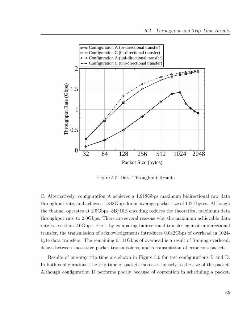
5.2 Throughput and Trip Time Results
32 64 128 256 512 1024 2048Packet Size (bytes)
0
0.5
1
1.5
2T
hrou
ghpu
t Rat
e (G
bps)
Configuration A (bi-directional transfer)Configuration C (bi-directional transfer)Configuration A (uni-directional transfer)Configuration C (uni-directional transfer)
Figure 5.5: Data Throughput Results
C. Alternatively, configuration A achieves a 1.918Gbps maximum bidirectional raw data
throughput rate, and achieves 1.848Gbps for an average packet size of 1024 bytes. Although
the channel operates at 2.5Gbps, 8B/10B encoding reduces the theoretical maximum data
throughput rate to 2.0Gbps. There are several reasons why the maximum achievable data
rate is less than 2.0Gbps. First, by comparing bidirectional transfer against unidirectional
transfer, the transmission of acknowledgements introduces 0.042Gbps of overhead in 1024-
byte data transfers. The remaining 0.111Gbps of overhead is a result of framing overhead,
delays between successive packet transmissions, and retransmission of erroneous packets.
Results of one-way trip time are shown in Figure 5.6 for test configurations B and D.
In both configurations, the trip-time of packets increases linearly to the size of the packet.
Although configuration D performs poorly because of contention in scheduling a packet,
65

5 High-Speed Communication Architecture Results
32 64 128 256 512 1024 2048Packet Size (bytes)
1
10
Pack
et T
rip-
time
(us)
Configuration BConfiguration D
Figure 5.6: One-Way Trip Time Results
configuration B achieves a one-way trip time of 1.232µs for a packet size of 32 bytes, and
a one-way trip time of 13.138µs for an average packet size of 1024 bytes. The latencies in
a typical data transfer will now be analyzed.
In a direct intra-chip transfer of a packet between a producer and a consumer via
FSL, the latency in trip-time is determined by the size of the packet and the width of the
words being transferred. Because a 4-byte word is used, the transfer of a 1024-byte packet
requires a latency of 256 cycles. In comparing this direct transfer to a transfer across the
SERDES interface, there are two intermediate points of storage in the SERDES logic that
add additional latency to the packet transfer.
First, to prevent a partial packet from being transmitted, the entire packet is stored
in the transmit buffer prior to transmission. This requires 256 cycles for a 1024-byte
66

5.3 Comparison Against Alternate Communication Mechanisms
Table 5.4: Latency in Trip Time of a 1024-byte Packet Transfer
Cycle Cycle Delaymin Delaymax
Event Countmin Countmax (µs) (µs)Producer to Transmit Buffer 256 256 4.096 4.096Transmit Buffer to Receive Buffer 256 256 4.096 4.096Receive Buffer to Consumer 256 256 4.096 4.096Internal Aurora/MGT Latencies:Transmit LL to Receive LL[44] 49.5 52.5 0.792 0.840Latency in CRC Engine[1] 6 6 0.096 0.096Total 823.5 826.5 13.176 13.224
packet. The packet is then transferred from the transmit buffer of one FPGA to the receive
buffer of another. This transfer introduces an additional 256 cycles of latency. The entire
packet must again be stored in the receive buffer in case an error occurs in transmission.
Therefore, once the entire packet is received, a final 256 cycles of latency are necessary to
transfer the error-free packet to the consumer. Table 5.4 summarizes these latencies and
shows two additional latencies introduced from the Aurora module and the CRC engine.
Any inconsistencies between Table 5.4 and Figure 5.6 are a result in inaccuracies in the
MicroBlaze-OPB measurement configuration. Tabulated throughput and trip time results
are available in Appendix A.
5.3 Comparison Against Alternate Communication
Mechanisms
To determine relative performance of the SERDES interface, the design was compared
against the following methods of communication:
1. A Simple FPGA-based 100BaseT Ethernet Protocol Stack
Previous work[38] implements a simplified software-driven protocol stack for commu-
nication over available Ethernet physical connectors. Throughput and trip time tests
are performed using this software-driven stack and compared against the SERDES
67

5 High-Speed Communication Architecture Results
interface.
2. Full TCP/IP FPGA-based 100BaseT Ethernet
uClinux[47] was ported to the Xilinx Multimedia board and netperf[48], an open-
source network analysis tool, was then modified to compile as a stand-alone uClinux
application. Resulting throughput and trip time measurements were again compared.
3. High-Speed Cluster Gigabit Ethernet
To compare against the means of communication commonly used for cluster-based
MD simulators such as NAMD, two Pentium 4 3.0GHz workstations were connected
through a switch on a high-speed Gigabit Ethernet cluster. The modified netperf
source was then compiled to the workstations, and measurements were again taken
and compared.
Figures 5.7 and 5.8, respectively, compare configurations A and B of Figures 5.1 and 5.2
against the alternate communication means. Again tabulated results are available in Ap-
pendix A.
As shown in Figure 5.7, configuration A achieves data throughput at approximately
three times greater magnitude than the cluster-based Gigabit Ethernet for packet sizes
beyond 256 bytes. Although Gigabit Ethernet has a theoretical maximum throughput of
1Gbps, it peaks at approximately 625Mbps because of delays in the processors to perform
computations and access memory. When compared against alternate FPGA-based commu-
nication mechanisms, the SERDES interface achieves approximately two orders of magni-
tude improvement over the simplified Ethernet protocol stack and full TCP/IP. Although
100baseT Ethernet supports a maximum data transfer rate of 100Mbps, each FPGA-based
mechanism performs significantly worse because both protocol stacks are implemented on
MicroBlaze processors clocked at 66MHz.
As shown in Figure 5.8, the latency in one-way communication through configuration
B is approximately one order of magnitude less than the cluster-based Ethernet, two or-
ders of magnitude less than the simplified Ethernet protocol stack, and three orders of
magnitude less than full TCP/IP. Again, the trip-time of packets between all methods of
Ethernet-based communication is limited by the performance of the communicating pro-
cessors. Furthermore, additional latencies are introduced in transmitting packets across
68
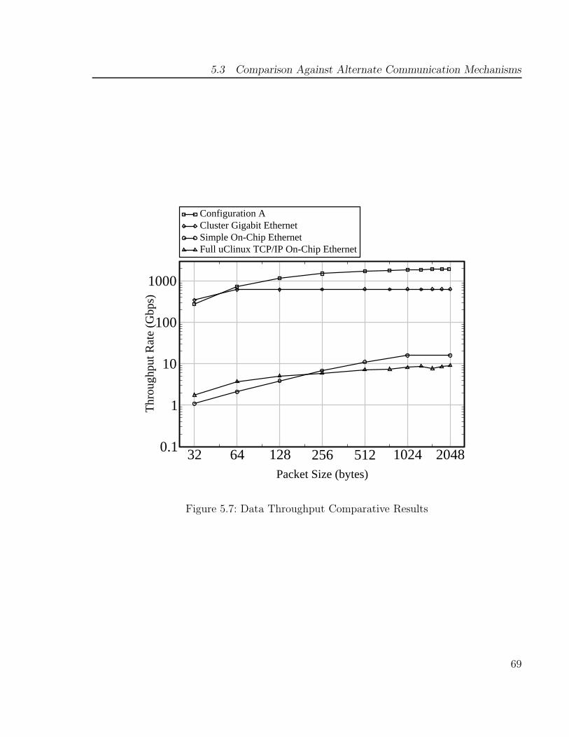
5.3 Comparison Against Alternate Communication Mechanisms
32 64 128 256 512 1024 2048Packet Size (bytes)
0.1
1
10
100
1000
Thr
ough
put R
ate
(Gbp
s)
Configuration ACluster Gigabit EthernetSimple On-Chip EthernetFull uClinux TCP/IP On-Chip Ethernet
Figure 5.7: Data Throughput Comparative Results
69

5 High-Speed Communication Architecture Results
32 64 128 256 512 1024 2048Packet Size (bytes)
1
10
100
1000
Pack
et T
rip-
time
(us)
Configuration BCluster Gigabit EthernetSimple On-Chip EthernetFull uClinux TCP/IP On-Chip Ethernet
Figure 5.8: Packet Trip Time Comparative Results
70

5.4 Design Area Usage
Figure 5.9: SERDES Logic Hierarchy
Ethernet communication devices such as switches. The FPGA-based simplified protocol
stack performs significantly better than full TCP/IP because a MicroBlaze processor can
traverse the reduced protocol quicker.
5.4 Design Area Usage
To determine the area usage of the SERDES core, the core was imported into Xilinx
Integrated Software Environment (ISE). The HDL code was mapped, and the resulting area
statistics, in terms of flip flops (FFs) and four-input look-up tables (LUTs) were extracted
from the map report. The process was repeated for submodules inside the design. A block
diagram to illustrate the hierarchy of the design is shown in Figure 5.9, and a description
of the different blocks is provided in Table 5.5.
Considerable overhead is a result of the debug logic discussed in Section 3.3. There-
fore, to determine the area necessary only for communication, the OPB register set and
sticky register interface were removed, and the design was re-mapped. Table 5.6 provides
a breakdown of the logic utilization, with and without debug logic, and Table 5.7 shows
the percent increase between the two designs as a result of the debug logic. The total area
of the SERDES interface is 2074 FFs and 2244 LUTs, which increase approximately 68%
and 43%, respectively, with the addition of debug logic. In Table 5.6, the remaining logic
of aurora connect consists of the remaining necessary OPB registers and logic to avoid
71

5 High-Speed Communication Architecture Results
Table 5.5: Hierarchical Block Description
Block Descriptioncc module clock correctionaurora aurora coretx handler transmit buffer, transmit error detectionrx handler receive buffer, receive error detectionufc tx handler acknowledge transmissionufc rx handler acknowledge receptionaurora connect system not including OPB and FSL interface logicfsl aurora system including OPB and FSL interface logic
Table 5.6: SERDES Interface Area Statistics
FFs % total FFs LUTs % total LUTsBlock Area Including Debug Logiccc module 9 0.2 6 0.2aurora 818 23.5 586 18.2tx handler 576 16.5 709 22.0rx handler 865 24.8 577 17.9ufc tx handler 17 0.5 101 3.1ufc rx handler 119 3.4 142 4.4aurora connect 3279 94.0 2149 66.8fsl aurora 3486 100.0 3218 100.0
Area Not Including Debug Logiccc module 9 0.4 6 0.3aurora 818 39.4 586 26.1tx handler 239 11.5 558 24.9rx handler 404 19.5 359 16.0ufc tx handler 17 0.8 101 4.5ufc rx handler 119 5.7 142 6.3aurora connect 1931 93.1 1704 75.9fsl aurora 2074 100 2244 100
72

5.5 Evaluation Against Architecture Requirements
Table 5.7: Debug Logic Area Statistics
Block FFs % increase FFs LUTs % increase LUTscc module 0 0 0 0aurora 0 0 0 0tx handler 337 141.00 151 27.06rx handler 461 114.11 218 60.72ufc tx handler 0 0 0 0ufc rx handler 0 0 0 0aurora connect 1348 69.81 445 26.12fsl aurora 1412 68.08 974 43.40
conflict between packets from different interfaces.
5.5 Evaluation Against Architecture Requirements
To conclude this chapter, the requirements presented in section 4.1 are reviewed.
1. Reliability
As discussed in Section 5.1, the SERDES interface because it has been tested across a
poor communications medium. In spite of a large amount of errors errors at the phys-
ical level, the SERDES implementation recovers predictably and sends data reliably.
Furthermore, communication is sustainable, and from the perspective of producers
and consumers, data transfer continues error-free for hours on end.
2. Low Area Consumption
A total area consumption of 2074 FFs and 2244 LUTs is currently required per
SERDES interface, requiring approximately 8% of the resources available on the
XC2VP30 series FPGA. Of the area consumed, approximately 39% of the FFs and
26% of the LUTs are from the Aurora core itself.
3. Minimal Trip Time
As presented in Section 5.2, a trip time of 13.138µs is achieved for an average packet
size of 1024 bytes. As indicated in Table 5.4, only a small percentage of this is latency
73

5 High-Speed Communication Architecture Results
is a result of data transfer through the Aurora or MGT, while the remaining latency
is necessary to ensure that partial packets are not transmitted and erroneous data is
not passed onward in the system.
4. Abstraction
By using the FSL interface, communication was achieved using a standard hardware
interface abstraction layer. Furthermore, the communication mechanism was incor-
porated into a programming model, as discussed in Chapter 6. Hence, a software
abstraction layer also exists.
With the evaluation of the SERDES interface complete, Chapter 6 will next incorpo-
rate the interface into a software-driven programming model. Chapter 7 will then draw
conclusions and discuss potential future work based upon these requirements.
74

6 A Simple Example: Integration into a
Programming Model
Based upon preliminary research of NAMD, Section 3.1 described an effective thread-based
programming model for molecular dynamics simulation. Since previous chapters of this
thesis have been written, the programming model for the TMD project has changed, where
a Message Passing Interface (MPI) communication method will instead be used.
Section 6.1 will first provide a light background on MPI. Then Section 6.2 describes how
the SERDES logic was incorporated into an MPI-based programming model. Section 6.3
concludes this chapter by providing communication results.
6.1 Background on MPI
In November, 1992, a preliminary draft proposal of MPI was put forward by Dongarra,
Hempel, Hey and Walker[49] with a goal to develop a widely used standard for writing
message passing programs. A meeting of over 40 organizations followed in January, 1993,
and a first version of MPI was released in June, 1994.
The first version of MPI provided a practical, portable, efficient and flexible standard
for message passing targeting Ethernet and Myrinet networking. This first version of the
library focused mainly on point-to-point routines, contained no implementations for collec-
tive communication routines, and was not thread-safe[50].
Subsequent versions of the library offered several improvements, including guaranteed
thread-safety of the existing function calls. Also, a series of collective communication
routines were added and several additional features, such as dynamic processes, one-sided
communication and parallel I/O were implemented. The most recent version of MPI,
75

6 A Simple Example: Integration into a Programming Model
version 2.0, was released in November 2003, and contains routines for 127 functions[50].
Several different modifications of the MPI library exist, and although previous work has
targeted MPI towards embedded systems[51], ongoing work in the TMD project[52] targets
MPI functions specifically to the MicroBlaze processor, where FSL links are the path of
communication. This subset of the MPI library implements the following routines for FSL-
based communication: MPI Recv, MPI Send, MPI Bcast, MPI Barrier and MPI Reduce.
6.2 Integration into the MPI-Based Programming Model
Because the FSL was used as an abstraction layer for the SERDES interface, from the
hardware perspective, integration of the SERDES interface was straightforward. A Mi-
croBlaze was connected to two four-byte wide, 16-word deep asynchronous FSLs, one for
transmitting data and a second for receiving data. The FSLs were then connected to a
producer input and a consumer output on the SERDES logic, respectively.
To send across the SERDES links, data must be encapsulated in the packet format
described in Figure 4.5. Furthermore, upon receiving incoming data from the SERDES
interface, the packet framing information must be removed. As described in Table 3.1, a
MicroBlaze processor communicates to an FSL via eight C function calls. The MPI library
uses these function calls, and to incorporate the SERDES interface into the MPI-based
programming model, the MPI function calls were modified. Because of time limitations,
only the MPI Send and MPI Recv functions were modified, and Figure 6.1 shows a small
segment of C code as an example where the modified MPI function calls were used. As seen
in this figure, a send is first issued by the processor. The first argument of this function
is an array containing the data to be transmitted. The second argument gives the number
of elements to be sent, and the third argument indicates the element type. The fourth
argument is a unique message tag that represents the message, and the final argument
indicates the MPI group for which the packet is intended. The processor then immediately
issues a receive for a packet. In this function, the first argument represents an array for the
incoming data and the fourth argument represents the source of the packet. The additional
seventh argument indicates the status of the receive and the remaining arguments are
the same. From a perspective of a software developer using MPI, this fragment of code
76

6.3 Software-Based Test Results
while (1) {
MPI_Send(data_outgoing, 64, MPI_INT, 0, 0, MPI_COMM_WORLD);
MPI_Recv(data_incoming, 64,
MPI_INT, 0, 0, MPI_COMM_WORLD, &status);
}
Figure 6.1: MPI Function Call Example
Consumers
Ack RX
Handler
Ack TX
Handler
LL
TXD
UFC
RXD
UFC
TXD
LL
RXD
MGT
AURORA
SERDES
Data RX
Handler
Data TX
Handler
SERDES
AURORA
MGTLL
RXD
UFC
TXD
UFC
RXD
LL
TXD
Ack TX
Handler
Ack RX
Handler
Data TX
Handler
Data RX
Handler
Data Status
Ack Status
Ack Status
Data Status
FSLs
....
....
....
Producers
....
....
....
FSLs
Consumers
....
....
....
FSLs
FSLs
....
....
....
Producers
FPGA x
xi
FPGA y
xj
xk
xl
xm
xn
yi
yj
yk
yl
ym
yn
Figure 6.2: MicroBlaze Configurations for Programming Model Integration
is platform-independent, and is directly portable to other environments, such as Linux.
Section 6.3 will now explain different hardware configurations in which the MPI function
calls were tested, and results of these tests are then provided.
6.3 Software-Based Test Results
Figure 6.2 is repeated from Chapter 4. By referring to this Figure, on FPGA x, a single Mi-
croBlaze replaces producer xi and consumer xl. On FPGA y, a second MicroBlaze replaces
producer yl and consumer yi. Hardware blocks were used for the remaining producers and
consumers, and Table 6.1 shows the different communication scenarios that were tested to
determine the performance of the MicroBlaze in the system. As can be seen by this table,
77

6 A Simple Example: Integration into a Programming Model
Table 6.1: Communication Scenarios for Programming Model Integration
Scenario Direction of TransferDescription
# VP7 toVP30
VP30 toVP7
1 xi → yi yl → xl MicroBlaze to MicroBlaze(no traffic from other producers and consumers)
2 xi → yi yl → xl MicroBlaze to MicroBlaze(traffic from other producers and consumers)
3 xi → yj yl → xm MicroBlaze to Hardware Consumer(no traffic from other producers and consumers)
4 xj → yi ym → xl Hardware Producer to MicroBlaze(no traffic from other producers and consumers)
Scenario 1 represents MicroBlaze-to-MicroBlaze communication, where each MicroBlaze
first sends, then receives a packet. Scenario 2 also represents MicroBlaze-to-MicroBlaze
communication, but while the MicroBlazes are communicating, all other hardware produc-
ers in the system are sending packets to respective hardware consumers. This scenario
analyzes the impact of additional traffic on MicroBlaze-to-MicroBlaze communication. In
Scenario 3, each MicroBlaze only sends data and rather than sending to the other MicroB-
laze, packets are instead sent to hardware consumer blocks. Finally, in Scenario 4, hardware
producer blocks send data to the MicroBlazes, and the MicroBlazes only receive packets
from these blocks.
Results are shown in Table 6.2 for 64 seconds of testing packets of 256 bytes in length
(not including an additional 32 bytes for packet framing). Several interesting observa-
tions are seen in these results. First, by comparing Scenarios 1 and 2 against Scenarios 3
and 4, MicroBlaze-to-MicroBlaze communication is approximately two times slower than
communication between MicroBlaze processors and hardware blocks. This is because, in
Scenarios 1 and 2, a MicroBlaze spends approximately half of its time sending a packet
and half of its time receiving a packet, resulting in a reduced throughput by each MicroB-
laze, compared to Scenario 3 where the MicroBlaze is only transmitting and in Scenario
4 where it is only receiving. Also, by comparing Scenarios 1 against Scenario 2, it is evi-
78

6.3 Software-Based Test Results
Table 6.2: Communication Results for Programming Model Integration
Scenario Number of Packets Transferred Approximate# VP7 to VP30 VP30 to VP7 Average Bit-Rate (Mbps)
1 537429 537429 537429 4.302 513069 513070 513069.5 4.103 971903 971896 971899.5 7.784 1112075 1112075 1112075 8.90
Table 6.3: Comparative Results for Programming Model Integration
Method of Communication Bit-Rate (Mbps)Scenario 1: MicroBlaze-based SERDES 4.30Simple Protocol Stack: MicroBlaze-based Ethernet 6.837Full TCP/IP: MicroBlaze-based Ethernet 5.915Configuration A: Hardware-based SERDES 1495.723
dent that traffic from other producers and consumers introduces very little overhead into
MicroBlaze-to-MicroBlaze communication.
Table 6.3 compares Scenario 1 against results presented in Section 5.2 for packets of
length 256 bytes. This table shows that MicroBlaze-based SERDES communication per-
forms worse than both methods of MicroBlaze-based communication via Ethernet. Fur-
thermore, Scenario 1 performs almost three orders of magnitude worse than SERDES com-
munication via dedicated producer and consumer hardware blocks.
There are several reasons why MicroBlaze-based SERDES communication performs
poorly. First, the MicroBlaze in this system operates at a clock rate of 40MHz. By com-
parison, the MicroBlaze in both Ethernet communication systems operates at 66MHz and
the producers and consumers of Configuration A operate at 62.5MHz. Furthermore, in
MicroBlaze-based SERDES communication, the rate at which a MicroBlaze accesses the
FSL is significantly less than the clock rate of the processor. Simulation results show that
54 clock cycles are required between subsequent non-blocking writes and 46 clock cycles
are required between subsequent non-blocking reads. This delay is the time required to
79

6 A Simple Example: Integration into a Programming Model
implement instructions and check for possible errors in the FSL transactions. By com-
parison, communication in the Ethernet communication system requires significantly fewer
clock cycles per transaction, and the producers and consumers in hardware-based SERDES
communication send and receive at a rate of one word per clock cycle.
Although these results seem discouraging, the purpose of this chapter is not to achieve
high performance in MicroBlaze-based SERDES communication. Instead, the work in this
chapter provides a mixed processor and hardware communication infrastructure for ongoing
work in the TMD project. As mentioned in Section 3.1, the first step in the TMD project
involves the development of an MD simulator in software to allow an easier debugging
environment and achieve a correct control structure. Current work has made significant
progress in this regard. Once this work is complete, compute-intensive software blocks
may be replaced by dedicated hardware engines, at which point the SERDES may be fully
utilized and significant speed-up may be obtained.
The work presented in this chapter, and in this thesis, provides a SERDES-based ca-
pability for preliminary software development and future dedicated hardware development.
Chapter 7 now draws conclusions and proposes future work with respect to the work pre-
sented in this thesis.
80

7 Conclusions and Future Work
Previous chapters address the complexity of molecular dynamics simulation, and motivate
the need for a high-speed communication mechanism for efficient simulation of complex
molecular problems. A variety of communication mechanisms are explored, and a reliable
SERDES-based communication capability was implemented for an FPGA-based solution
to the molecular dynamics problem. Assuming a 2.5Gbps bit-rate, the SERDES capability
achieves a maximum usable data throughput rate of 1.92Gbps. A minimum one-way trip
time of 1.232µs is achieved for a packet size of 32 bytes. The SERDES interface requires
2486 flip flops and 3218 look-up tables, but may be reduced to 2074 flip flops and 2244
look-up tables if all non-critical debug logic is removed. The SERDES interface uses a stan-
dard hardware abstraction interface, and has been integrated into a software programming
model.
Future work for the SERDES interface depends upon what bottle necks are introduced
in future development of the TMD project. For example, if the current sustainable bit-rate
is insufficient, the channel bonding capability of the Aurora module may be used, in which
several SERDES links may be combined into a single high-speed channel.
Furthermore, if future work determines that a reduced trip time is necessary, then
intermediate storage elements in the communication path could potentially be removed.
By guaranteeing that every producer can transmit data at 62.5×10⁶ words per second or
greater, a complete packet must no longer be stored in the transmit buffer before transmis-
sion and may immediately be sent upon being received. This would reduce the trip-time
of a 1024-byte packet by approximately 4.096µs. A second storage element at the receive
buffer ensures that a packet is received correctly before it is passed onward to the respective
consumer. Because this logic ensures that only an error-free packet is passed onward, the
removal of this storage element should be avoided. However, if an improved communication
81

7 Conclusions and Future Work
link is used, errors at the physical level may occur much less frequently. If, instead, errors
are handled by each consumer, the second storage element could be removed and packets
could be immediately passed to consumers with information on the errors that occurred.
Although the current implementation is effective at reliably communicating data across
the SERDES links, more complex protocols are possible which offer potential performance
improvements. For example, an obvious alternative to the current synchronous protocol is
an asynchronous protocol, where packets may be transmitted out-of-order. Furthermore,
a sliding window protocol, similar to that used in TCP/IP, could be used. In the sliding
window algorithm, a window of several packets are transmitted in order, and following error-
free receipt of packets, acknowledgements for all packets are sent by the receiver in-order.
Because acknowledgements are sent in-order, the transmitter does not need to receive every
acknowledgement. Hence, if an acknowledgement is received, then this packet, as well as
all prior packets, are acknowledged. If future bottlenecks deem it necessary, there may be
benefits to exploring the above two protocols in further detail.
Regardless of future design bottlenecks, the development work presented in this thesis
provides a strong framework for future development including multiple abstraction layers
and a useful run-time debugging capability. Furthermore, this work delivers a reliable
SERDES-based communication mechanism with reasonable area consumption and minimal
one-way packet trip time given current assumptions.
82

A Tabulated Throughput and Trip Time Results
APPENDIX
A Tabulated Throughput and Trip Time Results
The information presented in this Appendix is organized as follows:
1. Configuration A and Configuration C Throughput Results
2. Configuration B and Configuration D Trip-Time Results
3. Configuration A Throughput Comparative Results
4. Configuration C Trip-Time Comparative Results
83

Table A.1: Configuration A and Configuration C Throughput Results
Data Throughput (Gbps)Packet Size Bidirectional Transfers Unidirectional Transfers(bytes) Conf A Conf C Conf A Conf C
32 0.271 0.090 0.273 0.09064 0.723 0.249 0.750 0.247128 1.163 0.491 1.329 0.499256 1.496 0.822 1.617 0.829512 1.717 1.190 1.792 1.187768 1.803 1.375 1.856 1.3811024 1.848 1.421 1.889 1.4241280 1.876 1.145 1.910 1.1591536 1.895 1.023 1.923 1.0301792 1.908 0.949 1.933 0.9562016 1.918 0.906 1.940 0.911
Table A.2: Configuration B and Configuration D Trip-Time Results
Packet Trip-Time (µs)Packet Size(bytes) Conf B Conf D
32 1.232 1.92164 1.627 2.503128 2.389 3.818256 3.928 4.961512 6.995 9.182768 10.072 13.1841024 13.138 17.3411280 16.217 20.0061536 19.279 25.3571792 22.356 26.2532016 25.041 25.973
84

Table A.3: Configuration A Throughput Comparative Results
Data Throughput (Mbps)Packet Size Simple(bytes) Conf A Cluster Full TCP/IP Protocol
Stack
32 271.002 346.28 1.744 1.08464 723.214 615.5 3.724 2.116128 1163.435 619.21 5.028 3.865256 1495.723 624.42 5.915 6.837512 1717.298 624.96 7.165 11.111768 1802.517 622.7 7.361024 1847.635 626.85 8.173 15.8021280 1875.577 623.06 8.7411536 1894.561 628.73 7.6321792 1908.303 626.41 8.4912016 1917.7142048 627.68 9.085 16.025
85

Table A.4: Configuration B Trip-Time Comparative Results
Packet Trip-Time (µs)Packet Size Simple(bytes) Conf B Cluster Full TCP/IP Protocol
Stack
32 1.232 20.929 1071.834 164.16264 1.627 21.943 1083.917 172.804128 2.389 24.641 1160.039 190.084256 3.928 29.593 1258.812 227.526512 6.995 39.392 1475.71 299.528768 10.072 49.373 1677.9651024 13.138 57.128 1845.087 443.5331280 16.217 64.883 2058.2061536 19.279 74.142 2693.821792 22.356 78.454 2831.0972016 25.0412048 81.023 2903.938 918.742
86

References
[1] RocketIO Transceiver User Guide, version 2.5, Xilinx, Inc., 2004. [Online]. Available:http://www.xilinx.com/bvdocs/userguides/ug024.pdf
[2] S. Toyoda, et al., “Development of md engine: High-speed acceleration with paral-lel drocessor design for molecular dynamics simulations,” Journal of ComputationalChemistry, vol. 20(2), pp. 185–199, 1999.
[3] I. B. Team, “An overview of bluegene/l supercomputer,” in Proceedings of ACM Su-percomputing Conference, Baltimore, Maryland, November 2002.
[4] C. Anfinsen, “Principles that govern the folding of protein chains,” Science, vol. 181,pp. 223–230, 1973.
[5] P. J. Thomas, B.-H. Qu, and P. L. Pedersen, “Defective protein folding as a basis ofhuman disease,” Trends in Biochemical Sciences, vol. 20(11), pp. 456–459, 1995.
[6] S. B. Prusiner and S. J. DeArmond, “Prion diseases and neurodegeneration,” AnnualReview of Neuroscience, vol. 17, pp. 311–339, 1994.
[7] M. Allen and D. Tildesley, Computer Simulation of Liquids. Oxford University Press,Inc., 2002.
[8] T. Fukushige, et al., “A highly parallelized special-purpose computer for many-bodysimulations with an arbitrary central force: Md-grape,” The Astrophysical Journal,vol. 468, pp. 51–61, 1996.
[9] Y. Komeiji, et al., “Fast and accurate molecular dynamics simulation of a proteinusing a special-purpose computer,” Journal of Computational Chemistry, vol. 18(12),pp. 1546–1563, 1997.
[10] Y. Komeiji and M. Uebayasi, “Peach-grape system - a high performance simulator forbiomolecules,” Chem-Bio Informatics Journal, vol. 2(4), pp. 102–118, 2002.
87

[11] V. Pande, et al., “Atomistic protein folding simulations on the hundreds of microsecondtimescale using worldwide distributed computing,” Biopolymers, vol. 68, pp. 91–119,2003.
[12] S. Shirts and V. Pande, “Mathematical analysis of coupled parallel simulations,” Phys.Rev. Lett, vol. 86, pp. 4983–4987, 2001.
[13] Y. Rhee and V. Pande, “Multiplexed-replica exchange molecular dynamics method forprotein folding simulation,” Biophysical Journal, vol. 84, pp. 775–786, 2003.
[14] L. Kal, et al., “Namd2: Greater scalability for parallel molecular dynamics,” Journalof Computational Physics, vol. 151, pp. 283–312, 1999.
[15] J. C. Phillips, et al., “Namd: Biomolecular simulation on thousands of processors,” inProceedings of the IEEE/ACM SC2002 Conference, Baltimore, Maryland, 2002.
[16] T. Darden, D. York, and L. Pedersen, “Particle mesh ewald. an nlog(n) method forewald sums in large systems,” The Journal of Chemical Physics, vol. 98, pp. 10 089–10 092, 1993.
[17] Annapolis WILDCARDTM System Reference Manual, version 2.6, AnnapolisMicrosystems Inc., 2003. [Online]. Available: http://www.annapmicro.com
[18] J. F. Keane, C. Bradley, and C. Ebeling, “A compiled accelerator for biological cellsignaling simulations,” in Proceedings of the 2004 ACM/SIGDA 12th internationalsymposium on Field programmable gate arrays, vol. 12, Monterey, California, 2004,pp. 233–241.
[19] J. Davis, S. Akella, and P. Waddell, “Accelerating phylogenetics computing on thedesktop: Experiments with executing upgma in programmable logic,” in Proceedingsof EMBC-04: IEEE Electronics in Medicine and Biology Society Annual Conference,San Francisco, California, 2004.
[20] Mapstation Product Description, SRC Computers, Inc., 2004. [Online]. Available:http://www.srccomp.com/MAPstations.htm
[21] XD1 Datasheet, Cray Inc., 2005. [Online]. Available: http://www.cray.com/downloads/Cray XD1 Datasheet.pdf
[22] L. Cordova and D. Buell, “An approach to scalable molecular dynamics simulationusing supercomputing adaptive processing elements,” in Proceedings of FPL 2005: theInternational Conference on Field Programmable Logic and Applications, Tampere,Finland, 2005.
88

[23] Dongarra J. Linpack Benchmark, 2005. [Online]. Available: http://www.netlib.org/benchmark/linpackd
[24] Top500 Supercomputer Sites, 2005. [Online]. Available: http://www.top500.org
[25] K. Keeton, T. Anderson, and D. Patterson, “Logp quantified: The case for low-overhead local area networks,” in Proceedings of Hot Interconnects III: A Synposiumon High Performance Interconnects, Stanford, California, 1995.
[26] F. Wilder, A Guide to the TCP/IP Protocol Suite. Artech House, 1998, vol. 2, pp.25,125,169.
[27] C. Madill, 2005, private communication.
[28] Frequently Asked Questions, RapidIO Trade Association, 2005. [Online]. Available:http://www.rapidio.org/about/faq
[29] Frequently Asked Questions, HyperTransport Consortium, 2005. [Online]. Available:http://www.hypertransport.org/tech/tech faqs.cfm
[30] J. Brewer and J. Sekel, PCI Express Technology WhitePaper, 2004. [Online]. Available:http://www.dell.com/downloads/global/vectors/2004 pciexpress.pdf
[31] C. Sauer, et al., Towards a Flexible Network Processor Interface for RapidIO, Hyper-transport, and PCI-Express. Morgan Kaufmann Publishers, 2005, vol. 3, ch. 4, pp.55–80.
[32] M. Blumrich, et al., Design and Analysis of the BlueGene/L Torus InterconnectionNetwork, December 2003.
[33] IBM Research Blue Gene Project Page, 2005. [Online]. Available: http://www.research.ibm.com/bluegene
[34] MicroBlaze Soft Processor Core, Xilinx, Inc., 2005. [Online]. Available: http://www.xilinx.com/xlnx/xebiz/designResources/ip product details.jsp%?key=micro blaze
[35] PCI Platform FPGA Development Board Users Guide, version 6, AMIRIX SystemsInc., 2004. [Online]. Available: http://www.amirix.com
[36] MicroBlaze and Multimedia Development Board User Guide, version 1.0, Xilinx,Inc., 2002. [Online]. Available: http://www.xilinx.com/products/boards/multimedia/docs/UG020.pdf
89
[37] Fast Simplex Link (FSL) Bus, version 2.00.a, Xilinx, Inc., 2004. [Online]. Available:http://www.xilinx.com/bvdocs/ipcenter/data sheet/FSL V20.pdf
[38] P. Akl, 2004, private communication.
[39] On-Chip Peripheral Bus V2.0 with OPB Arbiter, version 1.10b, Xilinx, Inc., 2004.[Online]. Available: http://www.xilinx.com/bvdocs/ipcenter/data sheet/opb arbiter.pdf
[40] ChipScope Pro Software and Cores User Guide, version 6.3.1, Xilinx, Inc., 2004.[Online]. Available: http://www.xilinx.com/ise/verification/chipscope pro sw cores6 3i ug02%9.pdf
[41] A. Widmer and P. Franaszek, “A dc-balanced, partitioned-block, 8b/10b transmissioncode,” IBM J. Res. Develop., vol. 27(5), pp. 440–451, 1983.
[42] A. Tanenbaum, Computer Networks. Prentice Hall, 1996, vol. 3, ch. 3, pp. 187–190.
[43] Xilinx Core Generator, Xilinx, Inc., 2005. [Online]. Available: http://www.xilinx.com/xlnx/xebiz/designResources/ip product details.jsp%?key=dr dt coregenerator
[44] Aurora Reference Design User Guide, version 2.2, Xilinx, Inc., 2004. [Online].Available: http://www.xilinx.com/aurora/aurora member/ug061.pdf
[45] EG-2121CA-125.0000-LGPN Oscillator Data Sheet, Epson Electronics America, Inc.,2005. [Online]. Available: http://www.eea.epson.com/go/Prod Admin/Categories/EEA/QD/Crystal Oscill%ators/all oscillators/go/Resources/TestC2/EG2121 2102
[46] ITU-T Recommendation O.150 (Section 5.8), General Requirements for Instrumenta-tion for Performance Measurements on Digital Transmission Equipment, May 2003.
[47] J. Dionne and M. Durrant, uClinux Embedded Linux/Microcontroller Project, 2005.[Online]. Available: http://www.uclinux.org
[48] R. Jones, Netperf, Hewlett-Packard Company, 2005. [Online]. Available: http://www.netperf.org
[49] J. Dongarra, et al., “A proposal for a user-level, message-passing interface in a dis-tributed memory environment,” in Technical Report TM-12231, Oak Ridge NationalLaboratory, 1992.
[50] MPI-2: Extensions to the Message-Passing Interface, Message Passing InterfaceForum, 2003. [Online]. Available: http://www.mpi-forum.org/docs/mpi2-report.pdf
90

[51] R. Steele and R. Cunningham, “Ll/empi: An implementation of mpi for embeddedsystems,” in Proceedings of Scalable Parallel Libraries III, Mississippi State University,1996.
[52] M. Saldana, 2005, private communication.
91