Embed Size (px)
Citation preview
INTERNATIONAL JOURNAL OF PROFESSIONAL ENGINEERING STUDIES Volume V /Issue 5 /SEP 2015
IJPRES
A HIGH STEP-UP THREE-PORT DC–DC CONVERTER FOR STAND-ALONE PV/BATTERY POWER SYSTEM CONNECTED TO GRID
HIMASRI.VEMULA1, DR.N.MALLAREDDY2
M.Tech Student1, Associate Professor2
Department of EEE, G.Narayanamma Institute of Technology and Science, Hyderabad, India. E-mail: [email protected], [email protected]
Abstract—A three-port dc–dc converter integrating photovoltaic (PV) and battery power for high step-up applications with grid connected mode is proposed in this paper. The topology includes five power switches, two coupled inductors, and two active-clamp circuits. The coupled inductors are used to achieve high step-up voltage gain and to reduce the voltage stress of input side switches. Two sets of active-clamp circuits are used to recycle the energy stored in the leakage inductors and to improve the system efficiency. The operation mode does not need to be changed when a transition between charging and discharging occurs. Moreover, tracking maximum power point of the PV source and regulating the output voltage can be operated simultaneously during charging/discharging transitions. As long as the sun irradiation level is not too low, the maximum power point tracking (MPPT) algorithm will be disabled only when the battery charging voltage is too high. Therefore, the control scheme of the proposed converter provides maximum utilization of PV power most of the time. As a result, the proposed converter has merits of high boosting level, reduced number of devices, and simple control strategy. Development of the model and Simulation is done using MATLAB/SIMULINK software Index Terms—DC micro grid, energy storage, high step-up application, hybrid power system, renewable energy source, three-port converter.
I. INTRODUCTION
Integrated multiport converters for interfacing several power sources and storage devices are widely used in recent years. Instead of using individual power electronic converters for each of the energy sources, multiport converters have the advantages including less components, lower cost, more compact size, and better dynamic performance. In many cases, at least one energy storage device should be incorporated. For example, in the electric
vehicle application, the regenerative energy occurs during acceleration or startup. Therefore, it is very important for the port connected to the energy storage to allow bidirectional power flow.
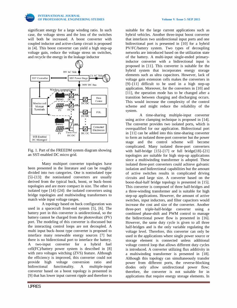
Various kinds of topologies have been proposed due to the advantages of multiport converters. The combination strategies for the multiport converter include sharing switches, capacitors, inductors, or magnetic cores [1]. One could select a proper topology by considering many aspects such as cost, reliability, and flexibility depending on the applications. An application of hybrid energy supply using renewable energy sources and storage devices is shown in Fig. 1. The dc micro grid enabled by the solid-state transformer (SST) in the Future Renewable Electric Energy Delivery and Management System (FREEDM System) integrates various distributed renewable energy resources (DRERs) and distributed energy storage devices (DESDs) [2]. For instance, if solar power is selected as the renewable energy source and battery as the storage device, the battery can either supply the load with the solar energy at the same time or store the excess power from the solar panels for backup use. Therefore, the bidirectional power path must be provided for the battery port. The dc–dc converters interfacing the DRERs or DESDs are expected to have relative high voltage conversion ratios since the dc bus of the FREEDM system is 380 V. It is studied that for the dc–dc converters connected to the solar panels, voltage gain extension cells such as coupled inductors, transformers, and switched capacitors are often employed to achieve high voltage conversion ratios [3]. By utilizing the voltage gain extension cells, the extreme duty cycles that exist in typical boost converters can be avoided and the voltage stress on switches can be reduced. Thus, power switches with lower voltage rating and lower turn-on resistance can be chosen for the converters to reduce conduction losses.
A converter using coupled inductors is relatively better than isolation transformers since the coupled inductors have simpler winding structure and lower conduction loss [4]. However, the leakage inductors of the coupled inductors will consume
INTERNATIONAL JOURNAL OF PROFESSIONAL ENGINEERING STUDIES Volume V /Issue 5 /SEP 2015
IJPRES
significant energy for a large winding ratio. In such case, the voltage stress and the loss of the switches will both be increased. A boost converter with coupled inductor and active-clamp circuit is proposed in [4]. This boost converter can yield a high step-up voltage gain, reduce the voltage stress on switches, and recycle the energy in the leakage inductor
Fig. 1. Part of the FREEDM system diagram showing an SST-enabled DC micro grid.
. Many multiport converter topologies have
been presented in the literature and can be roughly divided into two categories. One is nonisolated type [5]–[13]: the nonisolated converters are usually derived from the typical buck, boost, or buck–boost topologies and are more compact in size. The other is isolated type [14]–[24]: the isolated converters using bridge topologies and multiwinding transformers to match wide input voltage ranges.
A topology based on buck configuration was used in a spacecraft front-end system [5], [6]. The battery port in this converter is unidirectional, so the battery cannot be charged from the photovoltaic (PV) port. The modeling of this converter is discussed but the interacting control loops are not decoupled. A multi input buck–boost type converter is proposed to interface many renewable energy sources [7] but there is no bidirectional port to interface the battery. A two-input converter for a hybrid fuel cell(FC)/battery power system is described in [8] with zero voltages witching (ZVS) feature. Although the efficiency is improved, this converter could not provide high voltage conversion ratio and bidirectional functionality. A multiple-input converter based on a boost topology is presented in [9] that has lower input current ripple and therefore is
suitable for the large current applications such as hybrid vehicles. Another three-input boost converter that interfaces two unidirectional input ports and one bidirectional port is presented in [10] for a hybrid PV/FC/battery system. Two types of decoupling networks are introduced based on the utilization state of the battery. A multi-input single-ended primary-inductor converter with a bidirectional input is proposed in [11]. This converter is suitable for the hybrid system that incorporates energy storage elements such as ultra capacitors. However, lack of voltage gain extension cells makes the converters in [9]–[11] difficult to be used in a high step-up application. Moreover, for the converters in [10] and [11], the operation mode has to be changed after a transition between charging and discharging occurs. This would increase the complexity of the control scheme and might reduce the reliability of the system.
A time-sharing multiple-input converter using active clamping technique is proposed in [14]. The converter provides two isolated ports, which is overqualified for our application. Bidirectional port in [11] can be added into this time-sharing converter to form an isolated three-port converter but the power stage and the control scheme will become complicated. Many isolated three-port converters with half-bridge [15]–[17] or full bridge[18]–[21] topologies are suitable for high step-up applications since a multiwinding transformer is adopted. These isolated three-port converters could achieve galvanic isolation and bidirectional capabilities but the amount of active switches results in complicated driving circuits and large size. A converter based on the boost-dual-half bridge topology is presented in [15]. This converter is composed of three half-bridges and a three-winding transformer and is suitable for high step-up applications. However, the amount of active switches, input inductors, and filter capacitors would increase the cost and size of the converter. Another three-port triple-half-bridge converter using a combined phase-shift and PWM control to manage the bidirectional power flow is presented in [16]. However, the same duty cycle is given to all three half-bridges and is the only variable regulating the voltage level. Therefore, this converter can only be used in the applications where single power source or storage element is connected unless additional voltage control loop that allows different duty cycles is introduced. A converter utilizing flux additivity in a multiwinding transformer is presented in [18]. Although this topology can simultaneously transfer power from different ports, the reverse-blocking diodes only allow unidirectional power flow; therefore, the converter is not suitable for in applications that require energy storage elements. In
INTERNATIONAL JOURNAL OF PROFESSIONAL ENGINEERING STUDIES Volume V /Issue 5 /SEP 2015
IJPRES
[21], a three-port bidirectional converter with three active full-bridges, a three-winding transformer, and two series resonant tanks is reported. The transformer provides full isolation among all ports and wide input voltage range. The switching losses are reduced due to soft-switching operation. The full bridge topology is good for relative high power application but requires more power switches and complicated circuit design .Integrated three-port converters derived from a half-bridge converter are presented in [22]–[24] to interface PV and battery power. Small-signal modeling and decoupling network is introduced in [23] to design the compensators separately for the cross-coupled control loops. A family of three-port half-bridge converters is described in [24] and the primary circuit can function as a synchronous rectification buck converter. Therefore, the converters in [22]–[24] are suitable for stand-alone step-down applications. Many other multi-input topologies are discussed in [13] and [25].
In this paper, a high step-up three-port dc-dc converter for the hybrid PV/battery system is proposed with the following advantages: 1) High voltage conversion ratio is achieved by using coupled inductors; 2) Simple converter topology which has reduced number of the switches and associate circuits; 3) Simple control strategy which does not need to change the operation mode after a charging/discharging transition occurs unless the charging voltage is too high; and 4) Output voltage is always regulated at 380 V under all operation modes. It is noted that for the MPP-tracking converters, operating range has to be limited to the voltage less than the MPP voltage when the output voltage or current control is active [26]. This issue could be addressed by limiting the operating range of the converter in the voltages higher than MPP.As shown in Fig. 1, comparing to the typical multi converter configuration that requires individual microcontroller for each converter, the integrated three-port converters are controlled by a single microcontroller. The communication interface utilized in the multi converter configuration could be removed due to centralized control of the proposed converter.
Therefore, the system cost and volume can be reduced. The major contribution of this paper is to propose an integrated three-port converter as a nonisolated alternative other than typical isolated topologies for high step-up three-port applications. The proposed switching strategy allows the converter to be controlled by the same two duty cycles in different operation modes. The detailed analysis is given in the following sections: The principle of operation is described in Section II. The PV source
modeling, topological modes, and ZVS conditions are analyzed in Section III. The modeling and control strategy is explained in Section IV. Finally, the experimental results are presented in Section V.
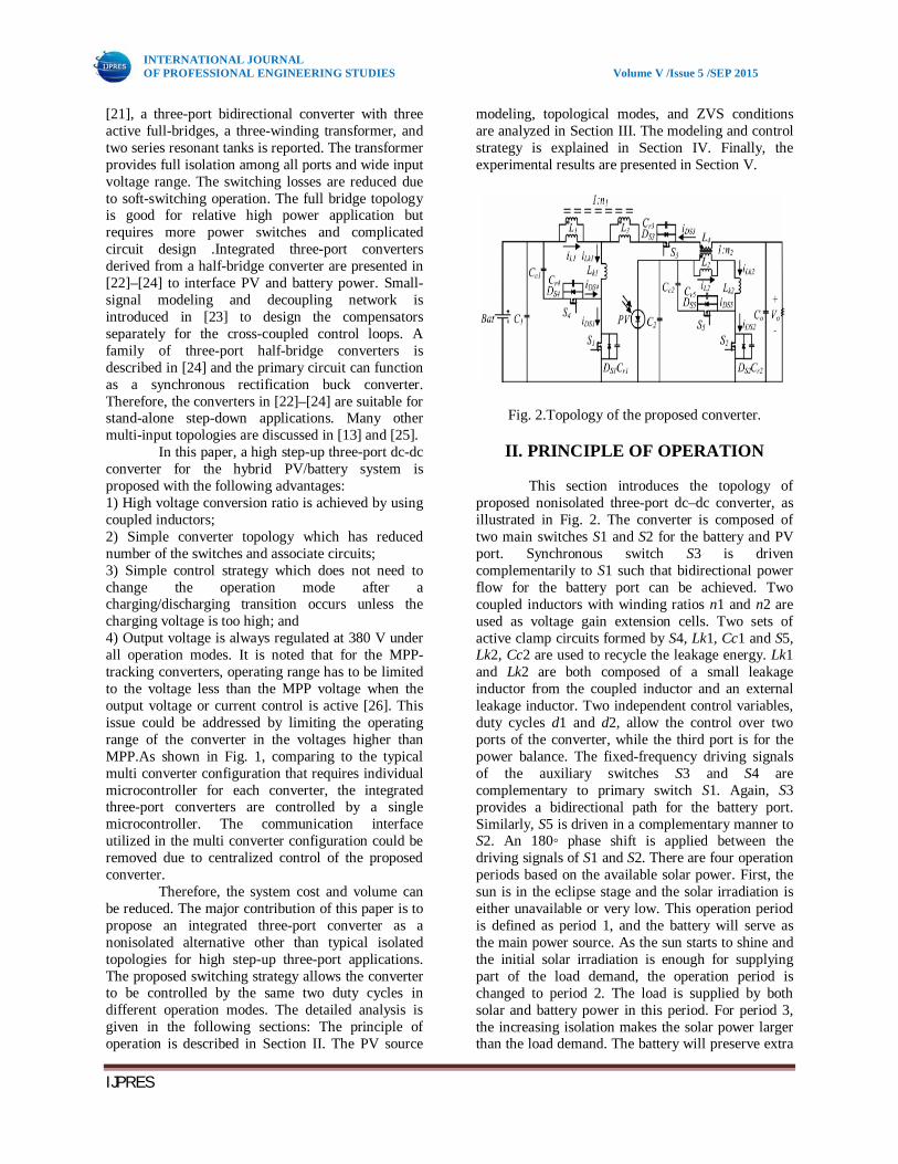
Fig. 2.Topology of the proposed converter.
II. PRINCIPLE OF OPERATION
This section introduces the topology of proposed nonisolated three-port dc–dc converter, as illustrated in Fig. 2. The converter is composed of two main switches S1 and S2 for the battery and PV port. Synchronous switch S3 is driven complementarily to S1 such that bidirectional power flow for the battery port can be achieved. Two coupled inductors with winding ratios n1 and n2 are used as voltage gain extension cells. Two sets of active clamp circuits formed by S4, Lk1, Cc1 and S5, Lk2, Cc2 are used to recycle the leakage energy. Lk1 and Lk2 are both composed of a small leakage inductor from the coupled inductor and an external leakage inductor. Two independent control variables, duty cycles d1 and d2, allow the control over two ports of the converter, while the third port is for the power balance. The fixed-frequency driving signals of the auxiliary switches S3 and S4 are complementary to primary switch S1. Again, S3 provides a bidirectional path for the battery port. Similarly, S5 is driven in a complementary manner to S2. An 180◦ phase shift is applied between the driving signals of S1 and S2. There are four operation periods based on the available solar power. First, the sun is in the eclipse stage and the solar irradiation is either unavailable or very low. This operation period is defined as period 1, and the battery will serve as the main power source. As the sun starts to shine and the initial solar irradiation is enough for supplying part of the load demand, the operation period is changed to period 2. The load is supplied by both solar and battery power in this period. For period 3, the increasing isolation makes the solar power larger than the load demand. The battery will preserve extra
INTERNATIONAL JOURNAL OF PROFESSIONAL ENGINEERING STUDIES Volume V /Issue 5 /SEP 2015
IJPRES
solar power for backup use. During period 4, the charging voltage of the battery reaches the preset level and should be limited to prevent overcharging. According to the solar irradiation and the load demand, the proposed three-port converter can be operated under two modes. In the battery balance mode (mode 1), maximum power point tracking (MPPT) is always operated for the PV port to draw maximum power from the solar panels. The battery port will maintain the power balance by storing the unconsumed solar power during light-load condition or providing the power deficit during heavy-load condition. The power sharing of the inputs can be represented as
(1) Where Pload is the load demand power, Ppv SVC is the PV power under solar voltage control (SVC), and Pbat SVC is the battery power under SVC. In mode 1, maximum power is drawn from the PV source. The battery may provide or absorb power depending on the load demand. Therefore, Pbat SVC could be either positive or negative. When the battery charging voltage is higher than the maximum setting, the converter will be switched into battery management mode (mode 2). In mode 2, MPPT will be disabled; therefore, only part of the solar power is drawn. However, the battery voltage could be controlled to protect the battery from overcharging. The power sharing of the inputs can be represented as
(2) Where Ppv BVC is the PV power under
battery voltage control (BVC) and Pbat BVC is the battery charging power under SVC. If the load is increased and the battery voltage is reduced, the converter will be switched to mode 1. The output voltage is always kept at 380 V in both modes.
III.TOPOLOGICAL MODES AND
ANALYSIS
A. PV Source Modeling
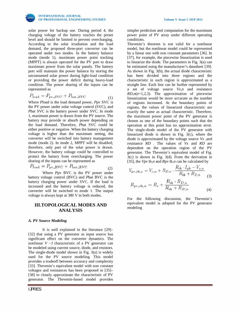
It is well explained in the literature [29]–[32] that using a PV generator as input source has significant effect on the converter dynamics. The nonlinear V −I characteristic of a PV generator can be modeled using current source, diode, and resistors. The single-diode model shown in Fig. 3(a) is widely used for the PV source modeling. This model provides a tradeoff between accuracy and complexity [33]. Thevenin’s equivalent model with non constant voltages and resistances has been proposed in [35]–[38] to closely approximate the characteristic of PV generator. The Thevenin-based model provides
simpler prediction and computation for the maximum power point of PV array under different operating conditions. Thevenin’s theorem is not valid for a nonlinear model, but the nonlinear model could be represented by a linear one with non constant parameters [36]. In [37], for example, the piecewise linearization is used to linearize the diode. The parameters in Fig. 3(a) can be estimated using the manufacturer’s datasheet [39]. As shown in Fig. 3(b), the actual diode characteristic has been divided into three regions and the characteristic in each region is approximated as a straight line. Each line can be further represented by a set of voltage source Vx,n and resistance RD,n(n=1,2,3). The approximation of piecewise linearization would be more accurate as the number of regions increased. At the boundary points of regions, the values of linearized characteristic are exactly the same as actual characteristic. Therefore, the maximum power point of the PV generator is chosen as one of the boundary points such that the operation at this point has no approximation error. The single-diode model of the PV generator with linearized diode is shown in Fig. 3(c), where the diode is approximated by the voltage source Vx ,and resistance RD . The values of Vx and RD are dependent on the operation region of the PV generator. The Thevenin’s equivalent model of Fig. 3(c) is shown in Fig. 3(d). From the derivation in [35], the Vpv th,n and Rpv th,n can be calculated by
(3)
(4) For the following discussion, the Thevenin’s equivalent model is adopted for the PV generator modeling
INTERNATIONAL JOURNAL OF PROFESSIONAL ENGINEERING STUDIES Volume V /Issue 5 /SEP 2015
IJPRES
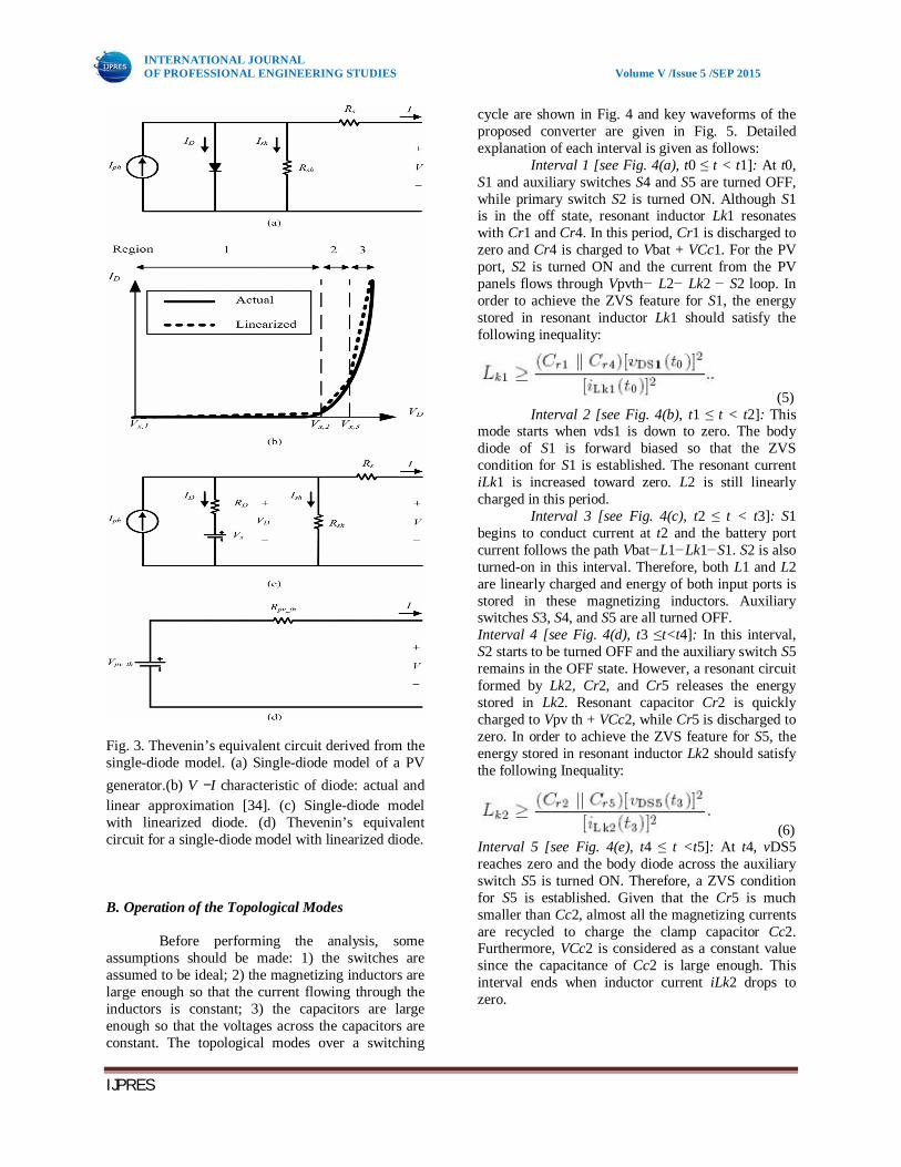
Fig. 3. Thevenin’s equivalent circuit derived from the single-diode model. (a) Single-diode model of a PV generator.(b) V −I characteristic of diode: actual and linear approximation [34]. (c) Single-diode model with linearized diode. (d) Thevenin’s equivalent circuit for a single-diode model with linearized diode. B. Operation of the Topological Modes
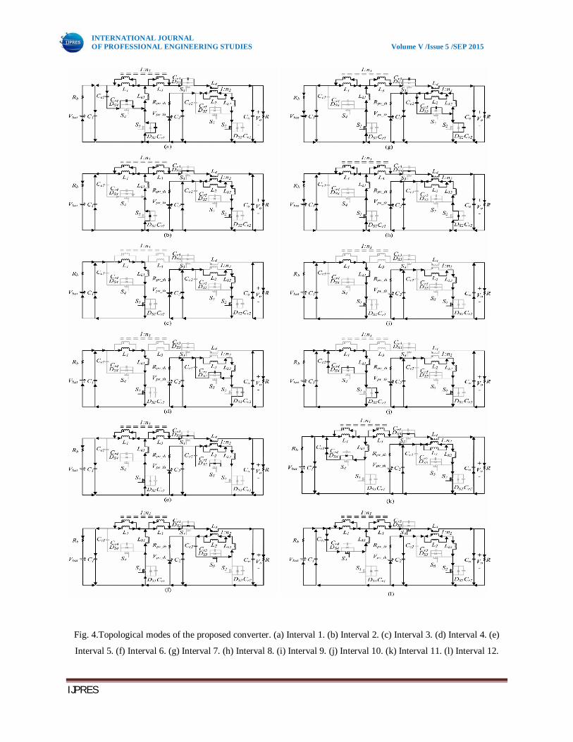
Before performing the analysis, some assumptions should be made: 1) the switches are assumed to be ideal; 2) the magnetizing inductors are large enough so that the current flowing through the inductors is constant; 3) the capacitors are large enough so that the voltages across the capacitors are constant. The topological modes over a switching
cycle are shown in Fig. 4 and key waveforms of the proposed converter are given in Fig. 5. Detailed explanation of each interval is given as follows:
Interval 1 [see Fig. 4(a), t0 ≤ t < t1]: At t0, S1 and auxiliary switches S4 and S5 are turned OFF, while primary switch S2 is turned ON. Although S1 is in the off state, resonant inductor Lk1 resonates with Cr1 and Cr4. In this period, Cr1 is discharged to zero and Cr4 is charged to Vbat + VCc1. For the PV port, S2 is turned ON and the current from the PV panels flows through Vpvth− L2− Lk2 − S2 loop. In order to achieve the ZVS feature for S1, the energy stored in resonant inductor Lk1 should satisfy the following inequality:
(5) Interval 2 [see Fig. 4(b), t1 ≤ t < t2]: This
mode starts when vds1 is down to zero. The body diode of S1 is forward biased so that the ZVS condition for S1 is established. The resonant current iLk1 is increased toward zero. L2 is still linearly charged in this period.
Interval 3 [see Fig. 4(c), t2 ≤ t < t3]: S1 begins to conduct current at t2 and the battery port current follows the path Vbat−L1−Lk1−S1. S2 is also turned-on in this interval. Therefore, both L1 and L2 are linearly charged and energy of both input ports is stored in these magnetizing inductors. Auxiliary switches S3, S4, and S5 are all turned OFF. Interval 4 [see Fig. 4(d), t3 ≤t<t4]: In this interval, S2 starts to be turned OFF and the auxiliary switch S5 remains in the OFF state. However, a resonant circuit formed by Lk2, Cr2, and Cr5 releases the energy stored in Lk2. Resonant capacitor Cr2 is quickly charged to Vpv th + VCc2, while Cr5 is discharged to zero. In order to achieve the ZVS feature for S5, the energy stored in resonant inductor Lk2 should satisfy the following Inequality:
(6) Interval 5 [see Fig. 4(e), t4 ≤ t <t5]: At t4, vDS5 reaches zero and the body diode across the auxiliary switch S5 is turned ON. Therefore, a ZVS condition for S5 is established. Given that the Cr5 is much smaller than Cc2, almost all the magnetizing currents are recycled to charge the clamp capacitor Cc2. Furthermore, VCc2 is considered as a constant value since the capacitance of Cc2 is large enough. This interval ends when inductor current iLk2 drops to zero.
INTERNATIONAL JOURNAL OF PROFESSIONAL ENGINEERING STUDIES Volume V /Issue 5 /SEP 2015
IJPRES
Fig. 4.Topological modes of the proposed converter. (a) Interval 1. (b) Interval 2. (c) Interval 3. (d) Interval 4. (e)
Interval 5. (f) Interval 6. (g) Interval 7. (h) Interval 8. (i) Interval 9. (j) Interval 10. (k) Interval 11. (l) Interval 12.
INTERNATIONAL JOURNAL OF PROFESSIONAL ENGINEERING STUDIES Volume V /Issue 5 /SEP 2015
IJPRES
Interval 6 [see Fig. 4(f), t5 ≤ t <t6]: At t5, the current of Lk2 is reversed in direction and energy stored in t5 is released through the Cc2−S5−Lk2−L3 loop. This interval ends when S5 is turned OFF. Interval 7 [see Fig. 4(g), t6 ≤ t <t7]: Switches S2 and S5 are both in the OFF state at t6 . A resonant circuit is formed by Lk2, Cr2, and Cr5. During this interval, Cr2 is discharged to zero and Cr5 is charged to Vpv th + VCc2. To ensure the ZVS switching of S2, the energy stored in Lk2 should be greater than the energy stored in parasitic capacitors Cr2 and Cr5
(7) Interval 8 [see Fig. 4(h), t7 ≤t<t8]: This interval starts when the voltage across Cr2 is zero and the body diode DS2 is turned ON. Leakage inductor current iLk2 is linearly increased and the secondary-side current of the coupled inductor is increased as well. The main switch S2 should be turned ON before iLk2 becomes positive to ensure ZVS operation. Interval 9 [see Fig. 4(i), t8 ≤ t < t9]: The circuit operation of interval 9 is identical to interval 3 since S1 and S2 are turned ON in both intervals. Interval 10 [Fig. 4(j), t9 ≤ t < t10]: At t9, S1 is turned OFF, while S3 and S4 remain in OFF state. During this interval, Lk1 will resonant with Cr1 and Cr4 to release the energy trapped in it. Resonant capacitor Cr1 is charged to Vbat + VCc1, while Cr4 is discharged to zero. To achieve the ZVS feature for S4, the energy stored in resonant inductor Lk2 should satisfy the following inequality:
(8) Interval 11 [see Fig. 4(k), t10 ≤ t < t11]: This interval begins when vDS4 drops to zero and the body diode across S4 is turned ON. The ZVS condition for S4 is then established. Almost all the magnetizing current is recycled to charge Cc1 since Cr4 is much smaller than Cc1. Moreover, VCc1 is considered as a constant value since the capacitance of Cc1 is large enough. This interval ends when inductor current iLk1 reaches zero. Interval 12 [see Fig. 4(l), t11 ≤ t < t12]: The current flow through Lk1 is reversed in direction at t11, and the energy stored in Cc1 is released through the Cc1−S4−Lk1−L1 loop. This interval ends when S4 is turned OFF and the operation of the proposed converter over a switching cycle is complete. .
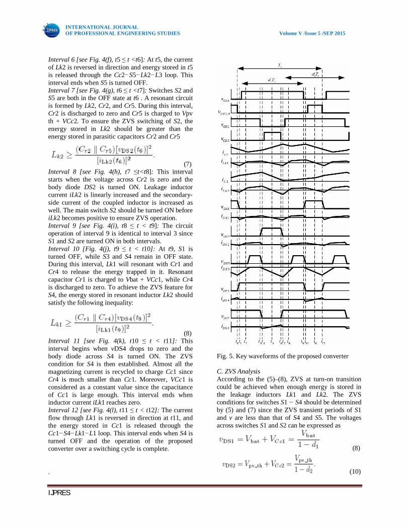
Fig. 5. Key waveforms of the proposed converter C. ZVS Analysis According to the (5)–(8), ZVS at turn-on transition could be achieved when enough energy is stored in the leakage inductors Lk1 and Lk2. The ZVS conditions for switches S1 − S4 should be determined by (5) and (7) since the ZVS transient periods of S1 and v are less than that of S4 and S5. The voltages across switches S1 and S2 can be expressed as
(8)
(10)
INTERNATIONAL JOURNAL OF PROFESSIONAL ENGINEERING STUDIES Volume V /Issue 5 /SEP 2015
IJPRES
The peak current flow through S1 and S2 can be obtained as
(11)
(12)
Where η represents the converter efficiency. It is noted that as long as L1 _ Lk1 and L2 _ Lk2, the behavior of the converter duty cycle is approximately the same as for the non active clamp converter in the continuous conduction mode. Typically, Lk1 = L1/10 and Lk2 = L2/10 can be the conservative design guidelines. The effective duty cycles deff1 and deff2 are assumed to be equal to d1 and d2 for subsequent equations. As a result, the following inequalities can be derived from (9)–(12) to determine a proper leakage inductor:
(13)
(14) IV. MODELING AND CONTROL STRATEGY
As mentioned in Section II, the operation
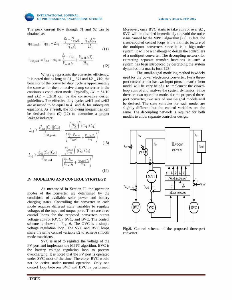
modes of the converter are determined by the conditions of available solar power and battery charging states. Controlling the converter in each mode requires different state variables to regulate voltages of the input and output ports. There are three control loops for the proposed converter: output voltage control (OVC), SVC, and BVC. The control scheme is shown in Fig. 6. The OVC is a simple voltage regulation loop. The SVC and BVC loops share the same control variable d2 to achieve smooth mode transitions.
SVC is used to regulate the voltage of the PV port and implement the MPPT algorithm. BVC is the battery voltage regulation loop to prevent overcharging. It is noted that the PV port is operated under SVC most of the time. Therefore, BVC would not be active under normal operation. Only one control loop between SVC and BVC is performed.
Moreover, once BVC starts to take control over d2 , SVC will be disabled immediately to avoid the noise issue caused by the MPPT algorithm [27]. In fact, the cross-coupled control loops is the intrinsic feature of the multiport converters since it is a high-order system. It will be a challenge to design the controllers of a multiport converter. The decoupling network for extracting separate transfer functions in such a system has been introduced by describing the system dynamics in a matrix form [23].
The small-signal modeling method is widely used for the power electronics converter. For a three-port converter that has two input ports, a matrix-form model will be very helpful to implement the closed-loop control and analyze the system dynamics. Since there are two operation modes for the proposed three-port converter, two sets of small-signal models will be derived. The state variables for each model are slightly different but the control variables are the same. The decoupling network is required for both models to allow separate controller design.
Fig.6. Control scheme of the proposed three-port converter.
INTERNATIONAL JOURNAL OF PROFESSIONAL ENGINEERING STUDIES Volume V /Issue 5 /SEP 2015
IJPRES
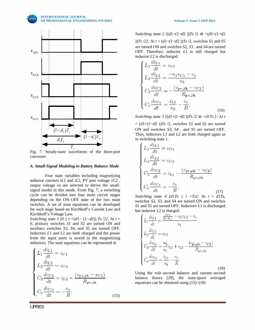
Fig. 7. Steady-state waveforms of the three-port converter. A. Small-Signal Modeling in Battery Balance Mode
Four state variables including magnetizing
inductor currents iL1 and iL2, PV port voltage vC2 , output voltage vo are selected to derive the small-signal model in this mode. From Fig. 7, a switching cycle can be divided into four main circuit stages depending on the ON–OFF state of the two main switches. A set of state equations can be developed for each stage based on Kirchhoff’s Current Law and Kirchhoff’s Voltage Law. Switching state 1 [0 ≤ t <(d1− (1−d2)) Ts /2]: At t = 0, primary switches S1 and S2 are turned ON and auxiliary switches S3, S4, and S5 are turned OFF. Inductors L1 and L2 are both charged and the power from the input ports is stored in the magnetizing inductors. The state equations can be represented in
(15)
Switching state 2 [(d1−(1−d2 ))Ts /2 ≤t <(d1+(1−d2
))Ts /2]: At t = (d1−(1−d2 ))Ts /2, switches S1 and S5 are turned ON and switches S2, S3 , and S4 are turned OFF. Therefore, inductor L1 is still charged but inductor L2 is discharged.
(16) Switching state 3 [(d1+(1−d2 ))Ts /2 ≤t <d1Ts ]: At t
= (d1+(1−d2 ))Ts /2, switches S1 and S2 are turned ON and switches S3, S4 , and S5 are turned OFF. Thus, inductors L1 and L2 are both charged again as in switching state 1.
(17) Switching state 4 [d1Ts ≤ t <Ts]: At t = d1Ts, switches S2, S3, and S4 are turned ON and switches S1 and S5 are turned OFF. Inductors L1 is discharged but inductor L2 is charged.
(18) Using the volt–second balance and current–second balance theory [28], the state-space averaged equations can be obtained using (15)–(18)
INTERNATIONAL JOURNAL OF PROFESSIONAL ENGINEERING STUDIES Volume V /Issue 5 /SEP 2015
IJPRES
(19)
(20)
(21)
(22) From (17)–(20), the state-space averaged model is shown as
(23) Based on the small-signal modeling method,
the state variables x, duty ratios d, and the port voltages v are considered to have the dc values (X, D,V)and perturbations (ˆx, ˆd, ˆv)
(24) Assume that the perturbations do not vary
significantly over a switching cycle (ˆx _ X, ˆ d _ D, ˆv _ V)and the small signal effect of Thevenin’s voltage source can be negligible (ˆvpvth = 0) [40]. One could substitute (24) into (15)–(18) and then average the four state equation sets regarding to their corresponding duty cycle. The last step is to neglect all of the second-order terms to obtain the small-signal model presented in matrix form
(25) Where x represents the state variable vector containing iL1, iL2, vC2, and vo, u represents the
control variable vector containing d1and d2, and y represents the output variable vector. In this case, the four state variables are also the system output. The small-signal model can be described as
(26)
Fig. 8. Small-signal model with decoupling network and compensators in the battery balance mode
Using this model, the transfer functions for the PV port voltage and output port voltage to the duty cycle values of the main switches could be obtained based on the small-signal diagram shown in Fig. 8. For the system of proposed converter, the state
INTERNATIONAL JOURNAL OF PROFESSIONAL ENGINEERING STUDIES Volume V /Issue 5 /SEP 2015
IJPRES
variables are controlled by two control variables. The transfer function matrix can be represented as
(27) Where G(j, k) represents the transfer
function of jth state variable to the kth control variable. These transfer functions can be calculated using the computer software such as MATLAB and are not presented because of their complexity. In order to design the closed-loop compensators separately, a decoupling network is introduced to decouple the interactive control loops [23]. In general derivation of the decoupling network, the state variable vector can be written as x = Gu*where u*is the modified input variable vector, u*= G*u. Therefore, x = GG*u and the goal here is to make GG*a diagonal matrix such that one output variable can be independently determined from one control input variable. According to G*= G−1xu−1,G*can be derived as
(28) Using (26)–(28), the system with cross-coupled control loops can be decoupled into a system with two independent control loops. The control loops (OVC and SVC loops) can be designed from the following equations:
(29) B. Small-Signal Modeling in Battery Manage Mode
The small-signal model in battery manage
mode can be derived by the same method. However, in this mode, the battery port voltage vC1 is considered as one of the state variables instead of the PV port voltage vC2. The four state variables are now iL1, iL2, vC1, and vo, while the control variables are still d1 and d2. The state-space averaged model in this mode could be represented as
(30)
Using (30), the small-signal model in this mode can be written as follows:
(31) Similarly, the decoupling network can be
used in this mode. The system control diagram with the decoupling network in battery manage mode is shown in Fig. 9. The transfer functions for the input and output voltage to duty cycle values can be extracted from the small-signal model. Therefore, the closed loop controllers for OVC loop and BVC loop can be designed separately

INTERNATIONAL JOURNAL OF PROFESSIONAL ENGINEERING STUDIES Volume V /Issue 5 /SEP 2015
IJPRES
(32)
(33)
Fig. 9. Small-signal model with decoupling network And compensators in the battery manage mode
Using equations (29) and (33), the system compensators could be designed with desired bandwidth, phase margin, and steady state error. For the proposed converter, an integration unit should be incorporated to eliminate the steady-state error of the system step responses. Although the steady-state error could be eliminated by adding an integral unit, the bandwidth would be reduced and may lead the system to be unstable.
To achieve proper phase margin of 60◦≤ P.M. ≤ 90◦ and enough bandwidth, a lead unit should also be included in addition to the integral unit since the integral unit will lower the cutoff frequency and decrease the phase margin. The bandwidth of the BVC and SVC could be designed to be about one decade lower than OVC to achieve tight load regulation.
Fig.10 Circuit Parameters
V. SIMULATION & RESULTS
A. Mat lab Modules
Figure 11 shows matlab model of photovoltaic system, and figure.12 shows the mat lab model of the three port DC-DC converter.
Fig 11. PV module
INTERNATIONAL JOURNAL OF PROFESSIONAL ENGINEERING STUDIES Volume V /Issue 5 /SEP 2015
IJPRES
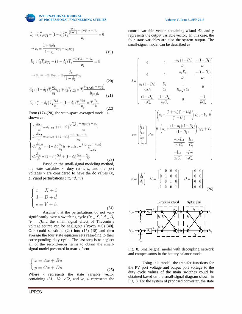
Fig 12 Matlab model of the three port circuit The control circuit is shown in figure 13 and
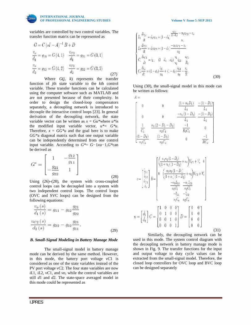
figure.14 shows the Maximum Power Point Tracking module designed based on the perturb and observe method.
Fig. 13 control circuit
Fig. 14 MPPT module
The DC output obtained is converted to ac by a three phase inverter. The figure 15 shows the matlab model of grid connection circuit. And figure 16 shows the matlab model of hysteresis controller.
Fig.15 connection to grid
INTERNATIONAL JOURNAL OF PROFESSIONAL ENGINEERING STUDIES Volume V /Issue 5 /SEP 2015
IJPRES
Fig.16 Hysteresis Controller
B. Results
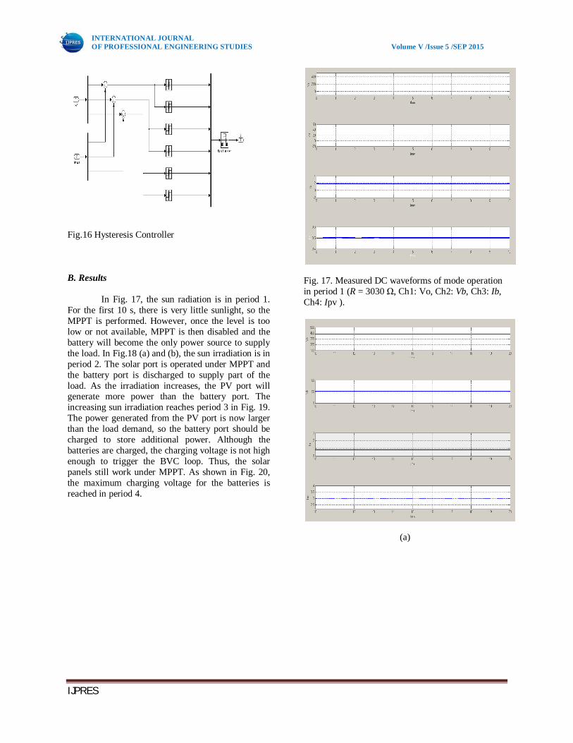
In Fig. 17, the sun radiation is in period 1. For the first 10 s, there is very little sunlight, so the MPPT is performed. However, once the level is too low or not available, MPPT is then disabled and the battery will become the only power source to supply the load. In Fig.18 (a) and (b), the sun irradiation is in period 2. The solar port is operated under MPPT and the battery port is discharged to supply part of the load. As the irradiation increases, the PV port will generate more power than the battery port. The increasing sun irradiation reaches period 3 in Fig. 19. The power generated from the PV port is now larger than the load demand, so the battery port should be charged to store additional power. Although the batteries are charged, the charging voltage is not high enough to trigger the BVC loop. Thus, the solar panels still work under MPPT. As shown in Fig. 20, the maximum charging voltage for the batteries is reached in period 4.
Fig. 17. Measured DC waveforms of mode operation in period 1 (R = 3030 Ω, Ch1: Vo, Ch2: Vb, Ch3: Ib, Ch4: Ipv ).
(a)
INTERNATIONAL JOURNAL OF PROFESSIONAL ENGINEERING STUDIES Volume V /Issue 5 /SEP 2015
IJPRES
(b)
Fig. 18 .Measured DC waveforms of mode operation in period 2. (a) Lower solar irradiation level. (b)Higher solar irradiation level (R = 1204 Ω, Ch1:Vo, Ch2: Vb, Ch3: Ib, Ch4: Ipv ).
Fig.19. Measured DC waveforms of mode operation in period 3 (R = 3030 Ω, Ch1:Vo, Ch2: Vb, Ch3: Ib, Ch4: Ipv ).
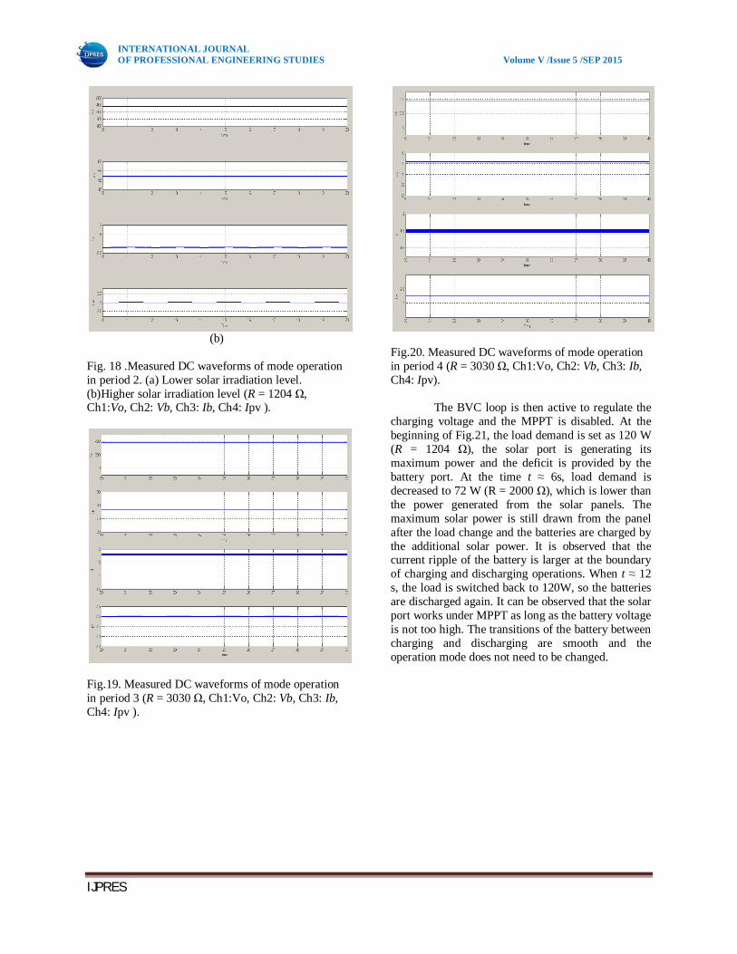
Fig.20. Measured DC waveforms of mode operation in period 4 (R = 3030 Ω, Ch1:Vo, Ch2: Vb, Ch3: Ib, Ch4: Ipv).
The BVC loop is then active to regulate the charging voltage and the MPPT is disabled. At the beginning of Fig.21, the load demand is set as 120 W (R = 1204 Ω), the solar port is generating its maximum power and the deficit is provided by the battery port. At the time t ≈ 6s, load demand is decreased to 72 W (R = 2000 Ω), which is lower than the power generated from the solar panels. The maximum solar power is still drawn from the panel after the load change and the batteries are charged by the additional solar power. It is observed that the current ripple of the battery is larger at the boundary of charging and discharging operations. When t ≈ 12 s, the load is switched back to 120W, so the batteries are discharged again. It can be observed that the solar port works under MPPT as long as the battery voltage is not too high. The transitions of the battery between charging and discharging are smooth and the operation mode does not need to be changed.
INTERNATIONAL JOURNAL OF PROFESSIONAL ENGINEERING STUDIES Volume V /Issue 5 /SEP 2015
IJPRES
Fig.21. Measured DC waveforms of load step response under SVC (Ch1:Vo, Ch2: Io , Ch3: Ipv, Ch4: Ib).
It should be noted that even during the load change, MPPT is achieved and the output voltage is well regulated. This is one of the important features of three-port converters since MPPT and load regulation could not be maintained simultaneously for typical two-port converters.
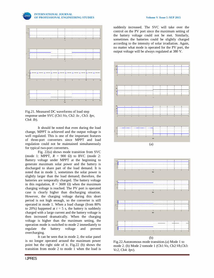
Fig. 22(a) shows mode transition from SVC (mode 1: MPPT, R = 900 Ω) to BVC (mode 2: Battery voltage under MPPT at the beginning to generate maximum solar power and the battery is discharged to share part of the load demand. It is noted that in mode 1, sometimes the solar power is slightly larger than the load demand; therefore, the batteries are temporally charged. The battery voltage in this regulation, R = 3600 Ω) when the maximum charging voltage is reached. The PV port is operated case is clearly higher than discharging situation. However, the charging voltage during this short period is not high enough, so the converter is still operated in mode 1. When a load change (from 80% to 20%) happened at t ≈ 5 s, the battery is suddenly charged with a large current and the battery voltage is then increased dramatically. When the charging voltage is higher than the maximum setting, the operation mode is switched to mode 2 immediately to regulate the battery voltage and prevent overcharging.
It can be seen that in mode 2, the solar panel is no longer operated around the maximum power point but the right side of it. Fig.22 (b) shows the transition from mode 2 to mode 1 when the load is
suddenly increased. The SVC will take over the control on the PV port since the maximum setting of the battery voltage could not be met. Similarly, sometimes the batteries could be slightly charged according to the intensity of solar irradiation. Again, no matter what mode is operated for the PV port, the output voltage will be always regulated at 380 V.
(a)
(b)
Fig.22.Autonomous mode transition.(a) Mode 1 to mode 2. (b) Mode 2 tomode 1 (Ch1:Vo, Ch2:Vb,Ch3: Vc2, Ch4: Ipv).
INTERNATIONAL JOURNAL OF PROFESSIONAL ENGINEERING STUDIES Volume V /Issue 5 /SEP 2015
IJPRES
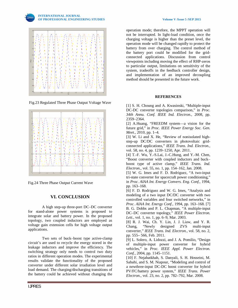
Fig.23 Regulated Three Phase Output Voltage Wave
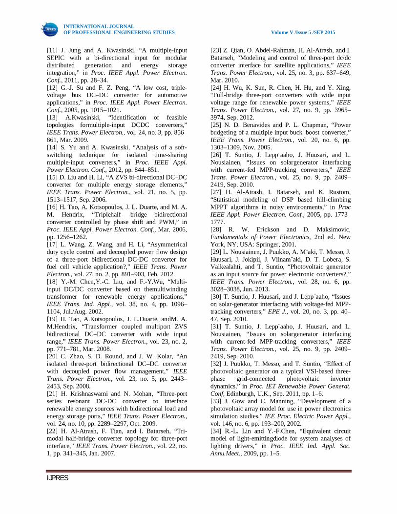
Fig.24 Three Phase Output Current Wave
VI. CONCLUSION
A high step-up three-port DC–DC converter for stand-alone power systems is proposed to integrate solar and battery power. In the proposed topology, two coupled inductors are employed as voltage gain extension cells for high voltage output applications.
Two sets of buck–boost type active-clamp circuit’s are used to recycle the energy stored in the leakage inductors and improve the efficiency. The switching strategy only needs to control two duty ratios in different operation modes. The experimental results validate the functionality of the proposed converter under different solar irradiation level and load demand. The charging/discharging transitions of the battery could be achieved without changing the
operation mode; therefore, the MPPT operation will not be interrupted. In light-load condition, once the charging voltage is higher than the preset level, the operation mode will be changed rapidly to protect the battery from over charging. The control method of the battery port could be modified for the grid-connected applications. Discussion from control viewpoints including moving the effect of RHP-zeros to particular output, limitations on sensitivity of the system, tradeoffs in the feedback controller design, and implementation of an improved decoupling method should be presented in the future work.
REFERENCES [1] S. H. Choung and A. Kwasinski, “Multiple-input DC-DC converter topologies comparison,” in Proc. 34th Annu. Conf. IEEE Ind. Electron., 2008, pp. 2359–2364. [2] A.Huang, “FREEDM system—a vision for the future grid,” in Proc. IEEE Power Energy Soc. Gen. Meet., 2010, pp. 1–4. [3] W. Li and X. He, “Review of nonisolated high-step-up DC/DC converters in photovoltaic grid-connected applications,” IEEE Trans. Ind. Electron., vol. 58, no. 4, pp. 1239–1250, Apr. 2011. [4] T.-F. Wu, Y.-S.Lai, J.-C.Hung, and Y.-M. Chen, “Boost converter with coupled inductors and buck–boost type of active clamp,” IEEE Trans. Ind. Electron., vol. 55, no. 1, pp. 154–162, Jan. 2008. [5] W. G. Imes and F. D. Rodriguez, “A two-input tri-state converter for spacecraft power conditioning,” in Proc. AIAA Int. Energy Convers. Eng. Conf., 1994, pp. 163–168. [6] F. D. Rodriguez and W. G. Imes, “Analysis and modeling of a two input DC/DC converter with two controlled variables and four switched networks,” in Proc. AIAA Int. Energy Conf., 1994, pp. 163–168. [7] B. G. Dobbs and P. L. Chapman, “A multiple-input DC–DC converter topology,” IEEE Power Electron. Lett., vol. 1, no. 1, pp. 6–9, Mar. 2003. [8] R. J. Wai, Ch. Y. Lin, J. J. Liaw, and Y. R. Chang, “Newly designed ZVS multi-input converter,” IEEE Trans. Ind. Electron., vol. 58, no. 2, pp. 555– 566, Feb. 2011. [9] L. Solero, A. Lidozzi, and J. A. Pomilio, “Design of multiple-input power converter for hybrid vehicles,” in Proc. IEEE Appl. Power Electron. Conf., 2004, pp. 1145–1151. [10] F. Nejabatkhah, S. Danyali, S. H. Hosseini, M. Sabahi, and S. M. Niapour, “Modeling and control of a newthree-input DC-DC boost converter for hybrid PV/FC/battery power system,” IEEE Trans. Power Electron., vol. 23, no. 2, pp. 782–792, Mar. 2008.
INTERNATIONAL JOURNAL OF PROFESSIONAL ENGINEERING STUDIES Volume V /Issue 5 /SEP 2015
IJPRES
[11] J. Jung and A. Kwasinski, “A multiple-input SEPIC with a bi-directional input for modular distributed generation and energy storage integration,” in Proc. IEEE Appl. Power Electron. Conf., 2011, pp. 28–34. [12] G.-J. Su and F. Z. Peng, “A low cost, triple-voltage bus DC–DC converter for automotive applications,” in Proc. IEEE Appl. Power Electron. Conf., 2005, pp. 1015–1021. [13] A.Kwasinski, “Identification of feasible topologies formultiple-input DCDC converters,” IEEE Trans. Power Electron., vol. 24, no. 3, pp. 856–861, Mar. 2009. [14] S. Yu and A. Kwasinski, “Analysis of a soft-switching technique for isolated time-sharing multiple-input converters,” in Proc. IEEE Appl. Power Electron. Conf., 2012, pp. 844–851. [15] D. Liu and H. Li, “A ZVS bi-directional DC–DC converter for multiple energy storage elements,” IEEE Trans. Power Electron., vol. 21, no. 5, pp. 1513–1517, Sep. 2006. [16] H. Tao, A. Kotsopoulos, J. L. Duarte, and M. A. M. Hendrix, “Triplehalf- bridge bidirectional converter controlled by phase shift and PWM,” in Proc. IEEE Appl. Power Electron. Conf., Mar. 2006, pp. 1256–1262. [17] L. Wang, Z. Wang, and H. Li, “Asymmetrical duty cycle control and decoupled power flow design of a three-port bidirectional DC-DC converter for fuel cell vehicle application?,” IEEE Trans. Power Electron., vol. 27, no. 2, pp. 891–903, Feb. 2012. [18] Y.-M. Chen,Y.-C. Liu, and F.-Y.Wu, “Multi-input DC/DC converter based on themultiwinding transformer for renewable energy applications,” IEEE Trans. Ind. Appl., vol. 38, no. 4, pp. 1096–1104, Jul./Aug. 2002. [19] H. Tao, A.Kotsopoulos, J. L.Duarte, andM. A. M.Hendrix, “Transformer coupled multiport ZVS bidirectional DC–DC converter with wide input range,” IEEE Trans. Power Electron., vol. 23, no. 2, pp. 771–781, Mar. 2008. [20] C. Zhao, S. D. Round, and J. W. Kolar, “An isolated three-port bidirectional DC–DC converter with decoupled power flow management,” IEEE Trans. Power Electron., vol. 23, no. 5, pp. 2443–2453, Sep. 2008. [21] H. Krishnaswami and N. Mohan, “Three-port series resonant DC-DC converter to interface renewable energy sources with bidirectional load and energy storage ports,” IEEE Trans. Power Electron., vol. 24, no. 10, pp. 2289–2297, Oct. 2009. [22] H. Al-Atrash, F. Tian, and I. Batarseh, “Tri-modal half-bridge converter topology for three-port interface,” IEEE Trans. Power Electron., vol. 22, no. 1, pp. 341–345, Jan. 2007.
[23] Z. Qian, O. Abdel-Rahman, H. Al-Atrash, and I. Batarseh, “Modeling and control of three-port dc/dc converter interface for satellite applications,” IEEE Trans. Power Electron., vol. 25, no. 3, pp. 637–649, Mar. 2010. [24] H. Wu, K. Sun, R. Chen, H. Hu, and Y. Xing, “Full-bridge three-port converters with wide input voltage range for renewable power systems,” IEEE Trans. Power Electron., vol. 27, no. 9, pp. 3965–3974, Sep. 2012. [25] N. D. Benavides and P. L. Chapman, “Power budgeting of a multiple input buck–boost converter,” IEEE Trans. Power Electron., vol. 20, no. 6, pp. 1303–1309, Nov. 2005. [26] T. Suntio, J. Lepp¨aaho, J. Huusari, and L. Nousiainen, “Issues on solargenerator interfacing with current-fed MPP-tracking converters,” IEEE Trans. Power Electron., vol. 25, no. 9, pp. 2409–2419, Sep. 2010. [27] H. Al-Atrash, I. Batarseh, and K. Rustom, “Statistical modeling of DSP based hill-climbing MPPT algorithms in noisy environments,” in Proc IEEE Appl. Power Electron. Conf., 2005, pp. 1773–1777. [28] R. W. Erickson and D. Maksimovic, Fundamentals of Power Electronics, 2nd ed. New York, NY, USA: Springer, 2001. [29] L. Nousiainen, J. Puukko, A. M¨aki, T. Messo, J. Huusari, J. Jokipii, J. Viinam¨aki, D. T. Lobera, S. Valkealahti, and T. Suntio, “Photovoltaic generator as an input source for power electronic converters?,” IEEE Trans. Power Electron., vol. 28, no. 6, pp. 3028–3038, Jun. 2013. [30] T. Suntio, J. Huusari, and J. Lepp¨aaho, “Issues on solar-generator interfacing with voltage-fed MPP-tracking converters,” EPE J., vol. 20, no. 3, pp. 40–47, Sep. 2010. [31] T. Suntio, J. Lepp¨aaho, J. Huusari, and L. Nousiainen, “Issues on solargenerator interfacing with current-fed MPP-tracking converters,” IEEE Trans. Power Electron., vol. 25, no. 9, pp. 2409–2419, Sep. 2010. [32] J. Puukko, T. Messo, and T. Suntio, “Effect of photovoltaic generator on a typical VSI-based three-phase grid-connected photovoltaic inverter dynamics,” in Proc. IET Renewable Power Generat. Conf, Edinburgh, U.K., Sep. 2011, pp. 1–6. [33] J. Gow and C. Manning, “Development of a photovoltaic array model for use in power electronics simulation studies,” IEE Proc. Electric Power Appl., vol. 146, no. 6, pp. 193–200, 2002. [34] R.-L. Lin and Y.-F.Chen, “Equivalent circuit model of light-emittingdiode for system analyses of lighting drivers,” in Proc. IEEE Ind. Appl. Soc. Annu.Meet., 2009, pp. 1–5.
INTERNATIONAL JOURNAL OF PROFESSIONAL ENGINEERING STUDIES Volume V /Issue 5 /SEP 2015
IJPRES
[35] A. Chatterjee and A. Keyhani, “Thevenin’s equivalent of photovoltaic source models for MPPT and power grid studies,” in Proc. IEEE Power Energy Soc. Gen. Meet., Jul. 2011, pp. 1–7. [36] Z. Batushansky and A.Kuperman, “Thevenin-based approach toPVarrays maximum power prediction,” in Proc. IEEE 26th Conv. Electr.Electron. Eng. Israel, Nov. 2010, pp. 000598–000602. [37] S. Chowdhury, G. A. Taylor, S. P.Chowdhury, A. K. Saha, andY. H. Song, “Modelling, simulation and performance analysis of a PV array in an embedded environment,” in Proc. Univ. Power Eng. Conf., 2007, pp. 781– 785. [38] H. Patangia, S. G. Gourisetti, A. Siddiqui, and S. Sharma, “A simplified PV model for low power MPPT controller design,” in Proc. IEEE Asia- Pacific Conf. Circuits Syst., 2010, pp. 680–683. [39] M. G. Villalva, J. R. Gazoli, and E. R. Filho, “Comprehensive approach to modeling and simulation of photovoltaic arrays,” IEEE Trans. Power Electron., vol. 24, no. 5, pp. 1198–1208, May 2009. [40] C. Hutchens, W. Yu, and J.-S. Lai, “Modeling and control of chargepumpedreboost converter for PV applications,” in Proc. IEEE Control Modeling Power Electron., 2010, pp. 1–5
Himasri.Vemula completed B.Tech. In Electrical & Electronics Engineering In 2013 From Sridevi Women’s Engineering College JNTUH, Hyderabad, Telangana And Pursuing M.Tech In Power Electronics And Drives From G.Narayanamma Institute Of Technology And Science, JNTUH, Hyderabad Telangana, India. Her Interests Are In The Area Of Power Electronics And Renewable Energy Sources.
E-mail id: [email protected]
Dr.N.MallareddyReddy, At Present Is An Associate Professor, Department Of Electrical and Electronics Engineering, G.Narayanamma Institute Of Technology And Science JNTUH, Hyderabad Telangana, India. He Received B.Tech. Degree In Electrical And Electronics Engineering From SV UNIVERSITY Tirupathi Andhra Pradesh. He Received M.Tech From J.N.T.U, Hyderabad, India and PHD from JNTUH. His Research Interests Accumulate in the Area of Power Electronics, Drives and power systems operation and control.
E-mail id: [email protected]