Embed Size (px)
Citation preview

A Linear RF Power Amplifier with High Efficiency for Wireless Handsets
Wael Yahia Refai
Dissertation submitted to the faculty of the
Virginia Polytechnic Institute and State University in partial fulfillment of the requirements for the degree of
Doctor of Philosophy
In
Electrical Engineering
William A. Davis, Chair Louis J. Guido
Mantu K. Hudait Werner E. Kohler Majid Manteghi
February 19, 2014 Blacksburg, VA
Keywords: power amplifier, power efficiency, linearity, broadband, matching network, impedance
transformation, converged power amplifier, wireless handset, class-J, GaAs HBT.
Copyright Wael Y. Refai, 2014 All rights reserved.

A Linear RF Power Amplifier with High Efficiency for Wireless Handsets
Wael Yahia Refai
ABSTRACT
This research presents design techniques for a linear power amplifier with high efficiency in
wireless handsets. The power amplifier operates with high efficiency at the saturated output power,
maintains high linearity with enhanced efficiency at back-off power levels, and covers a broadband
frequency response. The amplifier is thus able to operate in multiple modes (2G/2.5G/3G/4G). The
design techniques provide contributions to current research in handset power amplifiers, especially
to the converged power amplifier architecture, to reduce the number of power amplifiers within
the handset while covering all standards and frequency bands around the globe.
Three main areas of interest in power amplifier design are investigated: high power efficiency;
high linearity; and broadband frequency response. Multiple techniques for improving the
efficiency are investigated with the focus on maintaining linear operation. The research applies a
new technique to the handset industry, class-J, to improve the power efficiency while avoiding the
practical issues that hinder the typical techniques (class-AB and class-F). Class-J has been
implemented using GaN FET in high power applications. To our knowledge, this work provides
the first implementation of class-J using GaAs HBT in a handset power amplifier.
The research investigates the linearity, and the nature and causes of nonlinearities. Multiple
concepts for improving the linearity are presented, such as avoiding odd-degree harmonics, and
linearizing the relationship between the output current and the input voltage of the amplifier at the
fundamental frequency. The concept of bias depression in HBT transistors is introduced with a
bias circuit that reduces the bias-offset effect to improve linearity at high output power.
A design methodology is presented for broadband matching networks, including the
component loss. The methodology offers a quick and accurate estimation of component values,
giving more degrees of freedom to meet the design specifications. It enables a trade-off among
high out-of-band attenuation, number/size of components, and power loss within the network.
Although the main focus is handset power amplifiers, most of the developed techniques can
be applied to a wide range of power amplifiers.

ACKNOWLEDGEMENTS
First, I would like to express my sincere appreciation to my advisor Dr. William A. Davis for his
patience in guiding me through the research. His invaluable guidance and support assisted me
passing through the difficult times of the research.
I would like to thank TriQuint Semiconductor Inc. for sharing the TQHBT3 design kits with
Virginia Tech, sponsoring the tape-out of both the GaAs HBT die and the module laminate, and
measuring the implemented design. Special gratitude to: Dr. David Halchin (director of North
Carolina design center) for his decision to sponsor the tape-out of the GaAs die and the laminate,
Mr. Steve Brown for his efforts in sharing the TQHBT3 design kits with Virginia Tech, Mr.
Stephen Bachhuber for his valuable technical discussions and advice during the tape-out process,
Mr. David Lee for his efforts in setting up the automated test bench for measuring the modules,
and Ms. Donna Vasseur for her role in assembling the modules for testing.
Also, I would like to thank Keysight Technologies Inc., formerly Agilent Technologies Inc.,
for providing an educational license for “Advanced Design System” (ADS) software.
Finally, I’m grateful to my parents for their significant support and encouragement during my
graduate studies.
iii

TABLE OF CONTENTS
ABSTRACT .................................................................................................................................................. ii
ACKNOWLEDGEMENTS ......................................................................................................................... iii
TABLE OF CONTENTS ............................................................................................................................. iv
LIST OF FIGURES .................................................................................................................................... vii
LIST OF TABLES ....................................................................................................................................... xi
1. Introduction ............................................................................................................................................... 1
1.1 – Research Motivation ........................................................................................................................ 1
1.2 – Background ...................................................................................................................................... 3
1.2.1 – Power Efficiency ....................................................................................................................... 3
1.2.2 – Linearity .................................................................................................................................... 4
1.2.3 – Broadband Matching Networks ................................................................................................ 5
1.2.4 – Semiconductor Device Technology .......................................................................................... 6
1.2.5 – Power Amplifiers for Wireless Handsets .................................................................................. 6
1.3 – Dissertation Overview ...................................................................................................................... 7
2. High Efficiency Techniques for Linear Power Amplifiers ....................................................................... 9
2.1 – Introduction ...................................................................................................................................... 9
2.1.1 – Class-A Power Amplifier ........................................................................................................ 10
2.1.2 – Load-Pull Technique ............................................................................................................... 13
2.2 – Reduced Conduction Angle Operation .......................................................................................... 14
2.2.1 – Observations on the Fourier Series of a Truncated Sinusoid ................................................. 15
2.2.2 – The Optimum Load for Class-AB, B, and C ........................................................................... 18
2.2.3 – Maximum Linear Output Power and Power Efficiency of Ideal Class-B ............................... 19
2.2.4 – The Practical Implementation of Class-AB, B, and C Load ................................................... 21
2.3 – High Efficiency Utilizing the Generated Harmonics ..................................................................... 22
2.3.1 – The Real Power of Periodic Signals ....................................................................................... 23
2.3.2 – Class-J Operation .................................................................................................................... 26
2.3.3 – Class-F Operation ................................................................................................................... 36
2.4 – Summary ........................................................................................................................................ 37
Appendix ................................................................................................................................................. 38
A2.1 – Derivation of the Collector Current Components ................................................................... 38
3. Linearity in RF Power Amplifiers and Bias Circuits .............................................................................. 43
iv

3.1 – Introduction .................................................................................................................................... 43
3.2 – Nonlinearities in Power Amplifiers ............................................................................................... 44
3.2.1 – The Nature of Nonlinearities ................................................................................................... 44
3.2.2 – The Transistor Effect on Linearity .......................................................................................... 47
3.2.3 – HBT Design Considerations ................................................................................................... 49
3.3 – Measurements of Linearity ............................................................................................................ 52
3.3.1 – Two-tone Test ......................................................................................................................... 53
3.3.2 – Adjacent Channel Power Ratio (ACPR) ................................................................................. 54
3.3.3 – Error Vector Magnitude (EVM) .............................................................................................. 55
3.4 – HBT Bias Circuits .......................................................................................................................... 55
3.4.1 – Basic Bias Circuits .................................................................................................................. 56
3.4.2 – Enhanced Bias Circuits ........................................................................................................... 58
3.5 – HBT Bias Considerations............................................................................................................... 61
3.5.1 – Bias Depression ...................................................................................................................... 61
3.5.2 – Bias Circuits with a Linearization Feature .............................................................................. 63
3.5.3 – Ballast Resistor ....................................................................................................................... 64
3.6 – Summary ........................................................................................................................................ 68
4. A Design Methodology for Broadband Matching Networks .................................................................. 69
4.1 – Introduction .................................................................................................................................... 69
4.1.1 – Background ............................................................................................................................. 70
4.2 – Single-Section Networks................................................................................................................ 72
4.2.1 – The L-Network ........................................................................................................................ 74
4.2.2 – The T-Network ....................................................................................................................... 76
4.3 – Broadband Networks...................................................................................................................... 77
4.3.1 – Challenges of the Typical Design Approach .......................................................................... 79
4.3.2 – Design Example ...................................................................................................................... 79
4.4 – New Design Methodology ............................................................................................................. 82
4.4.1 – Features of the Proposed Design Approach ............................................................................ 83
4.4.2 – The Design Process Guidelines ............................................................................................... 87
4.4.3 – The Stagger-Tuning Considerations ....................................................................................... 88
4.4.4 – Design Example and Comparison ........................................................................................... 90
4.4.5 – Discussion ............................................................................................................................... 96
4.5 – Summary ........................................................................................................................................ 97
v

Appendix ................................................................................................................................................. 99
A4.1 – Assumptions ............................................................................................................................ 99
A4.2 – Derivation of the T-Network Design Equations ................................................................... 100
A4.3 – The Design Equations of the Pi-Network ............................................................................. 104
5. The Design of a Linear Power Amplifier with High Efficiency ........................................................... 107
5.1 – Introduction .................................................................................................................................. 107
5.2 – The Design Strategy ..................................................................................................................... 109
5.2.1 – High Efficiency Approach .................................................................................................... 110
5.2.2 – Linearity Approach ............................................................................................................... 111
5.2.3 – Class-J for High Efficiency and Linearity ............................................................................ 112
5.2.4 – Advantages of Class-J in Handset Power Amplifiers ........................................................... 113
5.2.5 – The Proposed Design Process ............................................................................................... 116
5.3 – A Power Amplifier Module Design ............................................................................................. 117
5.3.1 – Power Stage Design .............................................................................................................. 118
5.3.2 – Driver Stage Design .............................................................................................................. 126
5.4 – The Design Schematic and Layout .............................................................................................. 132
5.4.1 – Full Module Schematic ......................................................................................................... 132
5.4.2 – Power Amplifier Die Layout ................................................................................................. 132
5.4.3 – Module Laminate Layout ...................................................................................................... 134
5.5 – Simulation and Experimental Results .......................................................................................... 136
5.5.1 – Simulation Strategy ............................................................................................................... 136
5.5.2 - Simulation Results ................................................................................................................. 138
5.5.3 – Measurement Results ............................................................................................................ 142
5.5.4 – Discussion ............................................................................................................................. 149
5.6 – Summary ...................................................................................................................................... 151
6. Conclusion ............................................................................................................................................ 153
6.1 – Research Summary ...................................................................................................................... 153
6.2 – Conclusion ................................................................................................................................... 155
6.3 – Significance of the Research ........................................................................................................ 157
Bibliography ............................................................................................................................................. 159
vi

LIST OF FIGURES
Figure 1-1 – Different power amplifier module architectures. ....................................................... 2
Figure 2-1 – A Basic single-stage power amplifier. ..................................................................... 10
Figure 2-2 – A simplified I-V transfer characteristic of a transistor. ............................................ 11
Figure 2-3 – The collector current of the reduced conduction angle operation (normalized to the
maximum current (iC,Max)). .................................................................................... 15
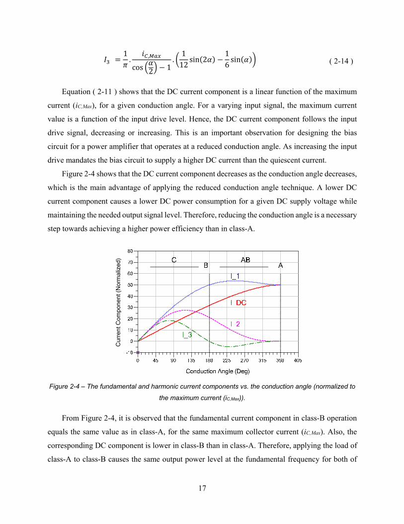
Figure 2-4 – The fundamental and harmonic current components vs. the conduction angle
(normalized to the maximum current (iC,Max)). ..................................................... 17
Figure 2-5 – A tank circuit represents an ideal load for a power amplifier that operates at a reduced
conduction angle. .................................................................................................. 18
Figure 2-6 – The resultant voltage waveform of a second harmonic component that is shifted by -
π/2 from the fundamental component (normalized to (VDC - VCE,EOS), the zero value
refers to VCE,EOS). .................................................................................................. 22
Figure 2-7 – A circuit shows the current and voltage signals at the collector/drain terminal of a
transistor. ............................................................................................................... 24
Figure 2-8 – Class-J voltage waveform - The effect of adding a second harmonic component in-
phase with the fundamental component (normalized to (VDC - VCE,EOS), the zero
value refers to VCE,EOS). ........................................................................................ 27
Figure 2-9 – The required load for class-J operation. ................................................................... 30
Figure 2-10 – Class-F voltage waveform - The effect of adding a third harmonic voltage
component to the fundamental component (normalized to (VDC - VCE,EOS), the zero
value refers to VCE,EOS). ........................................................................................ 36
Figure 2-11 – The collector current waveform as a truncated sinusoid (normalized to maximum
current). ................................................................................................................. 38
Figure 3-1 – Output power (Pout) vs. input power (Pin), and power gain (GP) vs. output power (Pout)
as input power (Pin) is swept. ................................................................................ 45
Figure 3-2 – The effect of bias point and reduced conduction angle on linearity. ....................... 48
Figure 3-3 – A simplified HBT large-signal model for operation in the active region. ............... 49
Figure 3-4 – A Base resistor to linearize the HBT characteristics. ............................................... 50
Figure 3-5 – An HBT Bias circuit with a bias resistor. ................................................................ 52
vii

Figure 3-6 – An equivalent circuit of the input section of a single-stage PA as shown in Figure 3-5.
............................................................................................................................... 52
Figure 3-7 – Spectrum of the two-tone signal, the generated IMDs and harmonics. ................... 53
Figure 3-8 – Adjacent channel power ratio (ACPR). ................................................................... 54
Figure 3-9 – Bias approaches of fixed base voltage, and fixed base current. ............................... 57
Figure 3-10 – A bias circuit of a single diode-connected transistor. ............................................ 58
Figure 3-11 – A bias circuit of a modified single-diode circuit with a base-current driver. ........ 59
Figure 3-12 – A bias circuit of double diode-connected transistors with an emitter follower. .... 60
Figure 3-13 – An HBT with DC blocking capacitor and a bias circuit. ....................................... 61
Figure 3-14 – An RF drive signal is coupled to a nonlinear load through a capacitor. ................ 62
Figure 3-15 – A Bias circuit of double-diodes with a linearization feature. ................................. 64
Figure 3-16 – Base ballast, and emitter ballast resistors. .............................................................. 65
Figure 3-17 – A bypassed base ballast resistor. ............................................................................ 66
Figure 3-18 – A bypassed base ballast resistor loaded by the input impedance of a transistor. ... 66
Figure 4-1 – The L-network, T-network, and Pi-network. ........................................................... 72
Figure 4-2 – Series and parallel impedance configurations. ......................................................... 73
Figure 4-3 – The down-transformation L-network. ...................................................................... 75
Figure 4-4 – The LCL T-network. ................................................................................................ 76
Figure 4-5 – A typical output matching network of a power amplifier. ....................................... 78
Figure 4-6 – The L-network with series inductor in the shunt branch. ......................................... 80
Figure 4-7 –The attenuation at out-of-band frequencies. .............................................................. 81
Figure 4-8 – The shift in frequency response and higher insertion loss. ...................................... 81
Figure 4-9 – The deviation in the real part of the transformed impedance from the targeted value
of 1.8 Ohm. ........................................................................................................... 82
Figure 4-10 – The proposed technique to design the matching network. ..................................... 83
Figure 4-11 – Comparison between the L-network and T-network. ............................................ 84
Figure 4-12 – The imaginary part of the transformed impedance of the down-transformation L-
network and T-network. ........................................................................................ 89
Figure 4-13 – The real part of the transformed impedance of the down-transformation L-network
and T-network. ...................................................................................................... 90
Figure 4-14 – The L-network with series inductor in the shunt branch. ....................................... 91
viii

Figure 4-15 – The LCL T-network with series inductor in the shunt branch. .............................. 92
Figure 4-16 – The real part of the transformed impedance. ......................................................... 94
Figure 4-17 – The frequency response.......................................................................................... 94
Figure 4-18 – The harmonics attenuation. .................................................................................... 95
Figure 4-19 – The power loss within the network. ....................................................................... 96
Figure 4-20 – A different configuration to analyze the matching network. ................................. 97
Figure 4-21 – The T-network. ..................................................................................................... 100
Figure 4-22 – The Pi-Network. ................................................................................................... 104
Figure 5-1 – The output and input sections of a single-stage power amplifier. .......................... 109
Figure 5-2 – A typical combined output matching network of a handset power amplifier. ....... 115
Figure 5-3 – Class-J output matching network requirements. .................................................... 116
Figure 5-4 – A block diagram of the power amplifier module. .................................................. 117
Figure 5-5 – Power stage: I-V DC transfer characteristics (simulated), collector current (iC) vs.
collector-emitter voltage (vCE) for steps of base-emitter voltage (vBE). ............. 120
Figure 5-6 – Output matching network. ...................................................................................... 122
Figure 5-7 – Power stage bias circuit. ......................................................................................... 124
Figure 5-8 – Approximated piecewise linear curve of collector current (iC) vs. base-emitter voltage
(vBE). ................................................................................................................... 124
Figure 5-9 – Driver stage: I-V DC transfer characteristics (simulated), collector current (iC) vs.
collector-emitter voltage (vCE) for steps of base-emitter voltage (vBE). ............. 127
Figure 5-10 – The inter-stage matching network. ....................................................................... 128
Figure 5-11 – Driver stage bias circuit. ...................................................................................... 129
Figure 5-12 – The input matching network. ............................................................................... 130
Figure 5-13 – A Feedback loop and an emitter inductance degeneration for stabilizing the driver
stage. ................................................................................................................... 131
Figure 5-14 – The full schematic of the power amplifier module. ............................................. 132
Figure 5-15 – The layout of the GaAs HBT die. ........................................................................ 133
Figure 5-16 – A photograph of the power amplifier die (bump pillars are pointing up). ........... 134
Figure 5-17 – The layout of the module laminate. ...................................................................... 135
Figure 5-18 – A photograph of the module laminate. ................................................................. 135
Figure 5-19 – EM simulation for S-parameters of an on-chip spiral inductor. ........................... 136
ix

Figure 5-20 – EM simulation for S-parameters of a printed Inductor on the laminate. ............. 137
Figure 5-21 – EM Simulation for S-parameters of the full module laminate. ............................ 138
Figure 5-22 – The simulated load impedance (real and imaginary parts) of the power stage. ... 139
Figure 5-23 – The collector current and voltage waveforms of the power stage. ...................... 140
Figure 5-24 – The simulated load impedance (real and imaginary parts) of the driver stage. ... 140
Figure 5-25 – The simulated power gain vs. output power at f0 (frequencies 815, 865, and 915
MHz). .................................................................................................................. 141
Figure 5-26 – The simulated phase difference between output and input signals vs. output power
at f0 (frequencies 815, 865, and 915 MHz). ........................................................ 141
Figure 5-27 – The simulated power added-efficiency vs. output power at f0 (frequencies 815, 865,
and 915 MHz). .................................................................................................... 142
Figure 5-28 – The fully assembled power amplifier module on evaluation board for testing. ... 143
Figure 5-29 – A block diagram of the test environment. ............................................................ 143
Figure 5-30 – 2G/GSM: The measured power gain vs. output power at f0 (multiple frequencies).
............................................................................................................................. 145
Figure 5-31 – 2G/GSM: The measured power-added efficiency (PAE) vs. output power at f0
(multiple frequencies). ........................................................................................ 145
Figure 5-32 – 2G/GSM: The measured second harmonic output power vs. output power at f0
(multiple frequencies). ........................................................................................ 146
Figure 5-33 – 2.5G/EDGE: The measured ACPR-200 (worst of upper/lower) vs. output power at
f0 (multiple frequencies). .................................................................................... 147
Figure 5-34 – 2.5G/EDGE: The measured EVM vs. output power at f0 (multiple frequencies). 148
Figure 5-35 – 3G/W-CDMA: The measured ACPR1 (worst of upper/lower) vs. output power at f0
(multiple frequencies). ........................................................................................ 149
x

LIST OF TABLES
Table 2-1 – The power amplifier classification based on the conduction angle. .......................... 14
Table 4-1 – The component values of the typical design process without loss. ........................... 80
Table 4-2 – The component values of design LLL_3S_Typ. ....................................................... 92
Table 4-3 – The component values of design TTT_3S. ................................................................ 92
Table 4-4 – The component values of design TT_2S. .................................................................. 92
Table 5-1 – The design targeted specifications. .......................................................................... 108
Table 5-2 – Test environment settings. ....................................................................................... 144
Table 5-3 – 2.5G/EDGE: test settings......................................................................................... 147
Table 5-4 – 3G/W-CDMA: test settings. .................................................................................... 148
xi
1
1.
Introduction
1.1–ResearchMotivation
The RF power amplifier is an important element in any wireless communications system. The
power amplifier provides a significant power amplification to the transmitted signal, leading to the
consumption of most of the system power. Hence, there is continuous research to improve the
power efficiency of the power amplifier and extend the battery lifetime of the handset.
The continuous growth in wireless communications applications has led to a fast growing
market of wireless handsets (such as cell phones and tablets). It has created an environment with
a high demand for better performance and higher data rates, and has led to the coexistence of
multiple industrial standards1 (2G/2.5G/3G/4G). Each standard utilizes a different modulation
scheme with different linearity requirements. For example, the 2G standard uses Gaussian
Minimum Shift Keying (GMSK) modulation that generates a constant envelope signal, not
requiring linear amplitude amplification. In contrast, the 4G standard utilizes Quadrature
Amplitude Modulation (QAM) which mandates a high degree of linear amplification.
The recent expansion of the cellular market has required more frequency bands to cover
multiple standards (2G/3G/4G). The spectrum that covers the cellular usage around the globe
(including most common bands) can be divided into three major bands: low band (695 MHz – 915
MHz), mid band (1710 MHz – 2025 MHz), and high band (2300 MHz – 2700 MHz). Each major
band is organized into many assigned narrower bands which are used in different regions around
the globe.
To meet the current market demands, handset manufacturers are targeting the design of a
single handset that covers the latest standards (3G/4G) with a backward compatibility to the earlier
standards (2G/2.5G), while exhibiting a broadband coverage over one or more of the major
frequency bands.
1 - The terms “standard” and “mode” are used throughout the dissertation referring to the cellular standard 2G/GSM, 2.5G/EDGE, 3G/W-CDMA, and 4G/LTE.

2
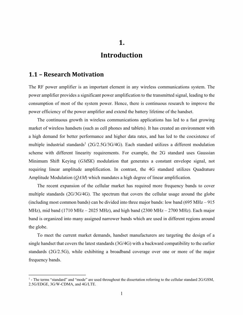
Different power amplifier architectures have been proposed to achieve such a coverage of
multiple standards with a broadband response, as shown in Figure 1-1. One power-amplifier
module architecture, known as a “hybrid power amplifier”, is to design a single module that
contains multiple power amplifiers. The architecture includes two power amplifiers for the
2G/2.5G modes where one covers the low band and the other covers the mid band. At least, three
more linear power amplifiers are needed for the 3G/4G modes, where each amplifier covers a part
or the full bandwidth of one of the major bands. Another architecture, known as a “converged
power amplifier”, is a single module that contains multiple power amplifiers, where each power
amplifier covers one of the major frequency bands while operating in different modes
(2G/2.5G/3G/4G).
LB
MB
HB
LB
MB
LB
MB
HB
3G/4G
2G/2.5G/3G/4G
2G/2.5G
HybridArchitecture
ConvergedArchitecture
Figure 1-1 – Different power amplifier module architectures.2
The two architectures show there is a trade-off between performance and cost/size. The hybrid
approach provides better performance since each power amplifier is dedicated to a specific mode
and a single frequency band. The converged approach provides less cost and board area,
2 - The “LB”, “MB”, and “HB” refer to the low, mid and high bands, respectively.

3
eliminating two or more power amplifiers with the associate matching networks. Typically the
power amplifiers that operate in the 2G/2.5G modes are the ones to be eliminated. The design
solution to a converged power amplifier architecture is required to exhibit three characteristics:
high linearity, high efficiency, and broadband frequency response in order to operate in the
different modes (2G/2.5G/3G/4G) with minimal or no reconfiguration as suggested by Cheng and
Young [1]. This solution is simpler in terms of cost and circuit complexity compared to more
complex architectures that require system integration such as those presented by McCune [2], and
Daehyun, et al. [3].
As a result, there is a demand for a linear power amplifier that operates with high efficiency
at the saturated output power level (in the 2G mode), maintains a high linearity with enhanced
efficiency at back-off output power levels (in the 2.5G/3G/4G modes), and covers a broadband
frequency response. Such a power amplifier represents a solution to the “converged power
amplifier” architecture. It should be noted, the required output power level in the 2G mode, is
higher than the required output power levels in the 2.5G/3G/4G modes where linearity is required.
Such a distribution of the needed power levels for these modes is suitable to be covered by a single
power amplifier, since the power amplifier would operate at the saturated power level in the 2G
mode and operates at back-off power levels in the 2.5G/3G/4G modes.
1.2–Background
Three major areas of interest in the power amplifier design are: achieving high power efficiency,
operating with high linearity, and covering a broadband frequency response.
1.2.1–PowerEfficiency
The power amplifier consumes the majority of the power in a wireless transmitter system. Hence,
there is continuous research to improve the power efficiency of the power amplifier. Over time,
different techniques to improve the power efficiency have been proposed, where each technique is
recognized as a class of power amplifier.
A fundamental technique to improve the efficiency of the power amplifier is to reduce the
quiescent bias level, which is known as the reduced conduction angle operation (class-AB, B, and
C). By reducing the quiescent bias level, the transistor conducts for a portion of the RF cycle rather
than a full RF cycle as in class-A operation.

4
A different technique to increase the power efficiency uses the generated harmonics within
the power transistor to engineer the voltage waveform at the collector/drain terminal of the
transistor. Class-F where the third harmonic is utilized, Raab [4], and class-J where the second
harmonic is utilized, Cripps, et al. [5], are examples of such a technique. It is important to note
that these techniques of utilizing the generated harmonics provide linear operation of the
fundamental frequency as well as improving the efficiency. Therefore, they are suitable for a linear
power amplifier application where a modulated signal of varying envelope is transmitted. One
variation of class-F is Class-AB/F, as presented by Daehyun, et al. [6], which can achieve linearity
and high efficiency at the maximum output power.
Another technique to obtain high power efficiency depends on operating the transistor as a
switch, such as class-D, El-Hamamsy [7], and class-E, Sokal and Sokal [8]. Due to the switching
operation of the transistor, no linear relationship exists between the amplitudes of the input and
output signals.3 Hence, such a technique is suitable to a power amplifier application where a
modulated signal with a constant envelope is transmitted since a linear operation is not required.
1.2.2–Linearity
The nonlinear operation of the power amplifier causes the generation of unwanted distortion
products, which extend out of the intended channel of the transmitted signal. The requirement for
linearity in radio frequency power amplifiers arises from the necessity of achieving minimum
interference with other channels in the frequency spectrum. Also, as cellular standards apply digital
modulation schemes, with both of the amplitude and phase are varying, the need for a linear power
amplifier increases, since the nonlinearity of the power amplifier causes not only a spectral
spreading, but also amplitude and phase distortions of the transmitted signal.
Different natures of nonlinearity occur in the power amplifier. The nonlinearities can be
categorized into a weak nonlinearity and a strong nonlinearity, Maas [9]. A weak nonlinearity
occurs when the power amplifier operates in the varying output power range. While the strong
nonlinearity appears when the power amplifier operates at the saturated output power.
The transistor characteristics have an effect on linear operation. For example, the exponential
relationship between the collector current and the base-emitter voltage of the HBT exhibits an
3 - The class-D is common at audio frequencies to obtain a linear output from a pulse-width modulated input at a switching rate far above the frequencies of use.

5
expansive transconductance4 that can be utilized to reduce the nonlinearity inherited from the
operation with a reduced conduction angle, Cripps [10]. Also, the elimination of the odd-degree
components at the output terminal of the transistor may improve the linearity, Cripps [11].
Utilizing an HBT transistor in a power amplifier shows a bias depression phenomenon that
degrades linearity at high output power. Such a behavior of HBT requires employing a bias circuit
that provides temperature compensation as well as a bias depression reduction in order to improve
linearity.
1.2.3–BroadbandMatchingNetworks
One technique of designing a matching network is to use tables of impedance-transforming
networks of low-pass filter form. Such tables are presented by Matthaei [12] for a Chebyshev
response and by Cristal [13] for a maximally-flat (Butterworth) response. This technique provides
a ladder network of series inductances and shunt capacitances.
Another technique of designing matching networks is based on single-section matching
networks of different topologies (L-network, T-network, and Pi-network). A set of design
equations for each topology is derived by combining the concepts of series/parallel resonance with
series/parallel impedance transformation. A broadband frequency response can be achieved by
cascading multiple sections.
The Smith chart has been used as a tool for designing lumped and distributed matching
networks. Both narrow-band and broadband matching networks can be designed using the Smith
chart following the typical topologies (L-network, T-network, and Pi-network), as presented by
Gonzalez [14]. In power amplifiers, the Smith chart provides an insight of the load that is presented
to the transistor since load-pull contours are usually plotted on the Smith chart.
Techniques of designing broadband matching networks using transformers have been
available for decades, as presented by Clarke and Hess [15]. Although, using transformers for
broadband matching networks provides better results compared to other techniques, it has a
restricted application in industry due to limitations that require designing for small die and module
size. Recently, investigations to implement on-chip transformers as part of output matching
networks were carried out, Hoseok, et al. [16].
4 - The transconductance increases as the input drive level increases.

6
1.2.4–SemiconductorDeviceTechnology
Gallium Arsenide (GaAs) semiconductor is one of the compound materials that enables low device
parasitics and high power density, making it suitable for high power and RF applications. High
band-gap semiconductors, such as Gallium Nitride (GaN), offers a high voltage operation and
higher power density compared to GaAs. Recently, GaN technology has seen a significant process
improvement and expansion in applications.
In the cellular industry, Laterally Diffused Metal Oxide Silicon (LDMOS) is used in high
power applications such as power amplifiers for base stations. GaAs HBT is widely used in low
power mobile devices, since it requires a single supply voltage a good feature in any application
where the circuit is supplied from a battery. As recent standards, such as 4G/LTE, specify a lower
output power, power amplifier designs using silicon CMOS technology have been investigated as
a replacement to GaAs HBT, Chang-Ho, et al. [17]. Recent results shows that silicon CMOS is
still not surpassing the linearity and high efficiency that GaAs HBT is providing.
GaAs HBT has more features making in the dominant technology of the power amplifier in
handsets. GaAs HBT exhibits a high power density, allowing for a smaller device size than other
technologies, saving on both die and module areas. With high linearity requirements, multiple
approaches can be applied to linearize the relationship between the output current and the input
voltage of an HBT-based amplifier at the signal frequency.
GaAs HBT process technology available from TriQuint has been selected to implement a
design that validates the techniques proposed in the research, TriQuint [18]. The process features
an InGaP emitter technology with a maximum junction current density of 20 kA/cm2.
1.2.5–PowerAmplifiersforWirelessHandsets
The typical power amplifier module for handsets consists of a multi-chip package. The module
includes a power amplifier (GaAs HBT) and a controller (silicon CMOS) providing the regulated
bias voltages needed for the power amplifier and other control signals. The module may also
include a silicon-on-insulator (SOI) switch that provides routing to different frequency bands. All
chips are mounted on a high frequency multi-layer laminate. Typically, the output matching
networks are implemented on the laminate. In order to reduce the number of discrete components,
almost all inductors in matching networks of power amplifier modules are printed planar inductors,
Franco [19].

7
1.3–DissertationOverview
The design of a linear power amplifier with high efficiency that covers a broadband frequency
response requires investigating three major areas of interest in the power amplifier design:
achieving high efficiency, operating with high linearity, and designing a broadband matching
network.
Chapter 2 presents multiple techniques to improve the power efficiency of a linear power
amplifier. The chapter presents a full analysis and investigations of the techniques with detailed
calculations of the required load impedance and the maximum theoretical efficiency that can be
achieved for each technique.
Chapter 3 presents investigations of the nonlinearities in RF power amplifiers. The chapter
presents the nature and causes of nonlinearities. The effect of operating the power amplifier in a
reduced conduction angle as well as the effect of odd-degree harmonics at the output of the
transistor are considered. The effect of HBT transistor on linearity is investigated, as well as
multiple bias circuits that provide temperature compensation and improved linearity.
Chapter 4 presents a new design methodology for matching networks. The methodology
considers the inductor loss in the design process and provides an accurate impedance
transformation while providing more degrees of freedom to meet a variety of specifications.
Chapter 5 introduces the proposed design process to achieve a linear power amplifier that
operates with high efficiency and can operate in different modes. The implemented power
amplifier module is presented as well as the simulated and measured results that validate the
proposed design process.
Chapter 6 presents the summary and the conclusion of the research.

8
(This page left intentionally blank)

9
2.
HighEfficiencyTechniquesforLinearPowerAmplifiers
2.1–Introduction
The power amplifier consumes the majority of the power in a wireless transmitter system. Hence,
there is continuous research to improve the power efficiency of the power amplifier. Over time,
different techniques to improve the power efficiency have been proposed, where each technique is
recognized as a class of power amplifier.
The class-A power amplifier is considered the simplest power amplifier, sharing many aspects
of the small-signal RF amplifier. However, class-A is not considered one of the high-efficiency
classes. The analysis of class-A is presented in this chapter to establish a reference for comparison
with the other high-efficiency classes, allowing many of the behaviors of the other classes to be
interpreted in terms of the operation of class-A.
A fundamental technique to improve the efficiency of the power amplifier is to reduce the
quiescent bias level, which is known as the reduced conduction angle operation (class-AB, B, and
C). By reducing the quiescent bias level, the transistor conducts for a portion of the RF cycle rather
than a full RF cycle as in class-A. Hence, the class-A and the other classic classes (class-AB, B,
and C) are defined based on the quiescent bias point.
A different technique to increase the power efficiency uses the generated harmonics within
the power transistor to engineer the voltage waveform at the collector/drain terminal of the
transistor. Class-F where the third harmonic is utilized, Raab [4], and class-J where the second
harmonic is utilized, Cripps, et al. [5], are examples of such a technique. It is important to note
that these techniques provide linear operation of the fundamental frequency as well as improving
the efficiency. Therefore, it is suitable for linear power amplifier applications where a modulated
signal of varying envelope is transmitted.
Another technique to obtain high power efficiency depends on operating the transistor as a
switch, such as class-D, El-Hamamsy [7], and class-E, Sokal and Sokal [8]. Due to the switching
operation of the transistor, no linear relationship exists between the amplitudes of the input and
output signals. Hence, such a technique is suitable to power amplifier applications where a
modulated signal with a constant envelope is transmitted since a linear operation is not required.

10
2.1.1–Class‐APowerAmplifier
A basic single-stage power amplifier that may represent a class-A power amplifier is shown in
Figure 2-1. In class-A power amplifier, the transistor is biased in the middle of the I-V transfer
characteristic. For linear operation, the current and voltage signals are constrained such that both
do not exceed the limits of cut-off and saturation.
RF_in
V_Reg
BiasCircuit
OutputMatchingNetwork
InputMatchingNetwork
R_L
V_DC
RFC
RF_out
Figure 2-1 – A Basic single-stage power amplifier.
Figure 2-2 shows a simplified I-V transfer characteristic of a typical transistor. Several key
assumptions are illustrated in the figure and maintained throughout this chapter and the following
chapters:
The output resistance of the transistor is infinite.
The transistor operates as a voltage-controlled current source with a linear
transconductance.
The reference plane of the load location is taken at the transistor output current source.
The associated output reactance of the transistor is considered to be a part of the output
matching network.

11
Figure 2-2 – A simplified I-V transfer characteristic of a transistor.
The optimum resistive load needed to obtain the maximum linear output power from a
transistor with the given I-V transfer characteristic in Figure 2-2 is computed as
, ,,
,
( 2-1 )
, , ( 2-2 )
,,
2 ( 2-3 )
where VCE,EOS is the edge of saturation voltage. The Vce,Max is the maximum voltage amplitude for
linear operation. The Ic,Max is the maximum current amplitude for linear operation. The iC,Max is the
maximum instantaneous collector current for a given transistor, which is determined by the
maximum current handling capability of the device. The VDC is the DC supply voltage which is
specified by the system. The IDC is the DC collector current component.
The optimum power (maximum linear output power) achieved by presenting the optimum
load to the transistor is calculated as
,12 , ,
12 , ( 2-4 )
The corresponding maximum power efficiency of class-A (ηMax,A) is given by

12
,
12 ,
( 2-5 )
where PL is the power delivered to the load (in Watts). The PDC is the consumed DC power (in
Watts). Assuming an ideal transistor where VCE,EOS is very small and approaching a value of zero,
then the efficiency for an ideal transistor (ηideal,A) is given by
,
12 50% ( 2-6 )
which is the well-known result of the ideal class-A power efficiency. From Equations ( 2-5 ) and
( 2-6 ), a general relationship between the maximum efficiency for a transistor with an edge of
saturation voltage (VCE,EOS) and the efficiency for an ideal transistor (VCE,EOS = 0) can be given as
, ( 2-7 )
Another term that is widely used to indicate the power efficiency is the power-added
efficiency (PAE)
( 2-8 )
where Pin is the input power (in Watts). The advantage of this form is it highlights both the
conversion of the DC power into the RF signal power and the power gain of the amplifier.
2.1.1.1–ObservationsonClass‐AOperation
The assumption that the transistor has a linear transconductance introduces a false expectation that
class-A is a fully linear power amplifier. Real transistors exhibit a weak nonlinearity within the
class-A region of operation. Operation at the optimum output power, where the full range of
current and voltage are utilized, forces the voltage and current to swing across the weakly-
nonlinear region. Therefore, in general, a class-A power amplifier is not a linear power amplifier.
Such an observation mandates presenting short-circuit terminations to the harmonic components
for proper operation of class-A.

13
For linear operation, the input drive should be maintained below the value that causes the
voltage and current to increase beyond the limits of cut-off or saturation. Once the voltage or
current reaches either cut-off or saturation, the output power starts to compress until it reaches the
1dB compression point.5 A further increase in the input drive signal leads to a higher compression
level to the point that the output power saturates.
Applying the optimum load, with the full range of voltage and current utilized, produces the
highest 1dB compression point as well as the highest maximum linear output power for a given
transistor. For a given maximum collector current (iC,Max), as the load deviates from the optimum
load, by increasing or decreasing the load, the 1dB compression point decreases as well as the
maximum linear output power. Decreasing the load reduces the available voltage swing and causes
the current to reach cut-off faster than the case of the optimum load. While, increasing the load
reduces the available current swing and causes the voltage signal to swing into the saturation region
of the transistor where the output current is function not only of the input voltage but also the
output voltage. As a result, increasing the load distorts the peak of the current waveform and
generates many harmonic components with high levels. This is an important observation in terms
of achieving the maximum range of linear operation for a given transistor, as a higher 1dB
compression point indicates a larger linear output power range.
2.1.2–Load‐PullTechnique
The load-pull technique is a fundamental method to determine the optimum load for a given
transistor through a laboratory measurement or simulation. At a single frequency, the technique is
implemented by tuning the load impedance presented to the collector/drain of the transistor.
Typically, the tuning is carried out on the impedance at the fundamental frequency while
presenting a constant impedance to harmonic components. Such an approach causes a major
limitation to determine the optimum load when implementing one of the advanced high-efficiency
classes, where the generated harmonics are employed to improve the power efficiency. An
advanced load-pull system, which is not widely exploited, would tune the impedance at the
fundamental as well as the second and third harmonic components, such as those introduced by
Benedikt, et al. [20] and Hashmi, et al. [21].
5 - The 1dB Compression point refers to the output power level where the large-signal gain has decreased by 1dB from the small-signal gain.

14
The results of the load-pull measurement is a plot on the Smith chart that contains a point
representing the optimum load that achieves the optimum output power. The plot typically contains
two or more contours, each contour representing a specified output power level lower than the
optimum power. It should be noted that during the load-pull measurement/simulation, the gain of
the amplifier may vary along each contour and the input power has to be adjusted accordingly to
maintain the output power level. Simple techniques to predict the load-pull contours for a transistor
that operates as a class-A power amplifier has been proposed, such as those by Cripps [22], and
Kondoh [23].
It is instructive to interpret those contours in terms of the complex power. Each contour can
be described as a contour for the same real power, but with a different apparent power (which is
the magnitude of the complex power). The minimum apparent power on each contour equals the
real power of the contour for the given transistor. Such a point of view indicates that applying a
load other than the optimum load may cause the transistor to operate at a higher power capacity
than what is really needed, in order to supply the additional reactive power.
2.2–ReducedConductionAngleOperation
The reduced conduction angle technique is a classic approach to achieve higher power efficiency
than what is typically offered by a class-A power amplifier. In class-A, the collector current
conducts during the full RF cycle (2π). The concept of the reduced conduction angle operation is
to bias the transistor at a lower quiescent bias point while the input drive signal turns on the
transistor during a portion of the RF cycle (< 2π), causing the collector current to conduct only
during that same portion. A classic set of operating classes of power amplifier (Class-AB, B, and
C) have been defined based on the conduction angle value, as shown in Table 2-1.
Class Conduction Angle A 2π (360O)
AB π (180O) - 2π (360O) B π (180O) C 0 – π (180O)
Table 2-1 – The power amplifier classification based on the conduction angle.

15
In order to utilize the maximum power capacity of the transistor, the full range of the collector
current should be used between cutoff and the maximum collector current (iC,Max). Therefore, when
operating at a reduced conduction angle, the input drive signal is required to increase compared to
the class-A operation in order to restore the peak of the collector current to the maximum value. A
typical observation is the power gain decreases as the conduction angle decreases. Figure 2-3
shows the instantaneous collector current, normalized to the maximum current, for each one of the
classes that are defined in Table 2-1, assuming the input drive signal is increased to generate a
collector current with a peak value that equals the maximum current.
Figure 2-3 – The collector current of the reduced conduction angle operation (normalized to the maximum
current (iC,Max)).
It should be noted that in order to achieve the highest possible power gain for a single-stage
power amplifier, it is generally found that the smallest transistor capable of delivering the needed
output power should be utilized. As the transistor periphery increases the power gain decreases,
which might cause a significant degradation in the power-added efficiency.
2.2.1–ObservationsontheFourierSeriesofaTruncatedSinusoid6
Due to the low quiescent bias point, the collector current takes the shape of a truncated sinusoid
when operating at a reduced conduction angle, as shown in Figure 2-3. A Fourier series analysis
6 - A detailed derivation of the DC, fundamental, and harmonic components, using the Fourier series analysis is presented in appendix A2.1.

16
is needed to understand the relationship between the frequency components of the collector current
(DC, fundamental, and harmonics) and the conduction angle. Following the analysis presented by
Cripps [10], it is assumed the input drive signal varies with the conduction angle to produce a
collector current waveform with a peak value equals the maximum current (iC,Max).
The instantaneous collector current is represented as
, cos ,2 2
0,2
,2
( 2-9 )
where Ic = iC,Max – IDC,Q, which is the amplitude of the generated current signal. The IDC,Q is the
quiescent DC collector current. The iC,Max is the maximum instantaneous collector current for the
given transistor. The α is the conduction angle. Writing the instantaneous collector current in terms
of iC,Max , and α
,
cos 2 1cos
2cos ,
2 2
0,2
,2
( 2-10 )
Applying Fourier series analysis to the instantaneous collector current given in Equation ( 2-10 ),
the DC current component is computed as
12
. ,
cos 2 1. cos
22 sin
2 ( 2-11 )
While the fundamental (I1), second (I2), and third (I3) harmonic current components are found to
be
1. ,
cos 2 1.12sin
2 ( 2-12 )
1. ,
cos 2 1.16sin
32
12sin
2 ( 2-13 )
17
1. ,
cos 2 1.112
sin 216sin ( 2-14 )
Equation ( 2-11 ) shows that the DC current component is a linear function of the maximum
current (iC,Max), for a given conduction angle. For a varying input signal, the maximum current
value is a function of the input drive level. Hence, the DC current component follows the input
drive signal, decreasing or increasing. This is an important observation for designing the bias
circuit for a power amplifier that operates at a reduced conduction angle. As increasing the input
drive mandates the bias circuit to supply a higher DC current than the quiescent current.
Figure 2-4 shows that the DC current component decreases as the conduction angle decreases,
which is the main advantage of applying the reduced conduction angle technique. A lower DC
current component causes a lower DC power consumption for a given DC supply voltage while
maintaining the needed output signal level. Therefore, reducing the conduction angle is a necessary
step towards achieving a higher power efficiency than in class-A.
Figure 2-4 – The fundamental and harmonic current components vs. the conduction angle (normalized to
the maximum current (iC,Max)).
From Figure 2-4, it is observed that the fundamental current component in class-B operation
equals the same value as in class-A, for the same maximum collector current (iC,Max). Also, the
corresponding DC component is lower in class-B than in class-A. Therefore, applying the load of
class-A to class-B causes the same output power level at the fundamental frequency for both of
Cur
rent
Com
pone
nt (
Nor
mal
ized
)
18
the classes, but a lower DC power consumption is achieved in class-B, leading to a higher power
efficiency. It is interesting to note that the second harmonic current component exists with a
relatively high level in class-B (about 42% of the fundamental component), while all odd-order
harmonic components equal zero in class-B.
As the conduction angle decreases below π, which is defined as class-C, both the fundamental
and the DC current components decrease. This decrease causes a reduction in the DC power
consumption as well as the output power at the fundamental frequency. Due to the reduction of
the output power and the requirement to increase the input drive signal, class-C typically suffers
from a much lower power gain than in class-A.
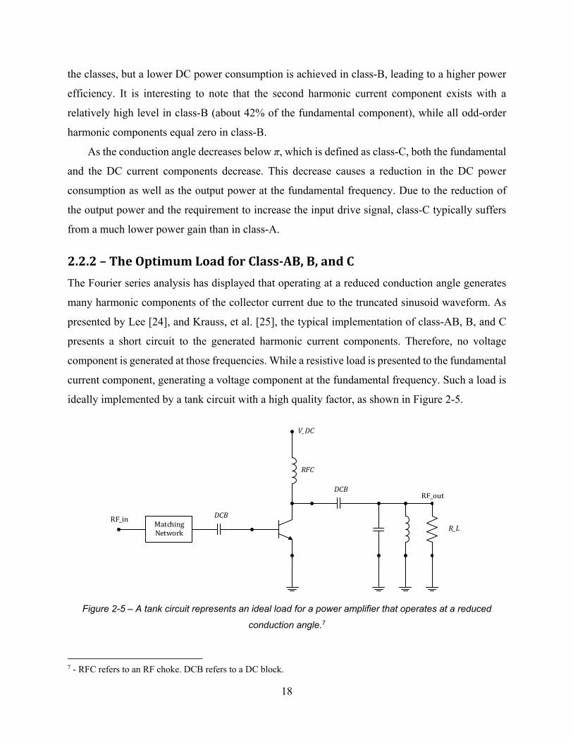
2.2.2–TheOptimumLoadforClass‐AB,B,andC
The Fourier series analysis has displayed that operating at a reduced conduction angle generates
many harmonic components of the collector current due to the truncated sinusoid waveform. As
presented by Lee [24], and Krauss, et al. [25], the typical implementation of class-AB, B, and C
presents a short circuit to the generated harmonic current components. Therefore, no voltage
component is generated at those frequencies. While a resistive load is presented to the fundamental
current component, generating a voltage component at the fundamental frequency. Such a load is
ideally implemented by a tank circuit with a high quality factor, as shown in Figure 2-5.
RF_in
V_DC
RF_out
RFC
MatchingNetwork
R_L
DCB
DCB
Figure 2-5 – A tank circuit represents an ideal load for a power amplifier that operates at a reduced
conduction angle.7
7 - RFC refers to an RF choke. DCB refers to a DC block.

19
The tank circuit represents an ideal implementation that approximates the real output matching
network. Realistic power amplifiers, operating in class-AB, B, and C, are implemented with an
output matching network that contains two or more matching sections. These networks exhibit
some non-ideal effects at the harmonic frequencies that must be considered in the final design.
Operating at a reduced conduction angle, in order to achieve the maximum output power from
a given transistor with the I-V transfer characteristic shown in Figure 2-2, the maximum peak of
the input drive signal is required to produce a collector current with a peak value equals the
maximum collector current (iC,Max). For each conduction angle of operation, there is a specific
fundamental current component produced. The optimum load is determined as the resistive load
to allow the fundamental voltage amplitude to reach the maximum value (VDC – VCE,OS), as shown
in Figure 2-2. Hence, the optimum load can be calculated by
,,
,
( 2-15 )
, , ( 2-16 )
where VCE,EOS is the edge of saturation voltage. The Vce1,Max is the maximum voltage amplitude of
the fundamental component. The Ic1,Max is the maximum current amplitude of the fundamental
component for a current waveform that reaches the maximum instantaneous current (iC,Max).
It should be noted that in order to maintain linear operation, the transistor should not be
overdriven, where the drive signal increases beyond the value that causes the collector current to
reach the maximum current (iC,Max). Overdriving the transistor causes the collector current
waveform to be clipped, generating a high level of harmonic components. Also, the load at the
fundamental frequency should not increase such that the collector voltage signal swings into the
saturation region. Such a situation causes many higher harmonic current components to be
generated with a higher level and mixed within the transistor.
2.2.3–MaximumLinearOutputPowerandPowerEfficiencyofIdeal
Class‐B
Many high efficiency techniques for linear power amplifiers rely on biasing the transistor in deep
class-AB (ideal class-B). In order to establish a reference for comparison with high efficiency

20
techniques, it is necessary to calculate the optimum output power (maximum linear power) and
the power efficiency of an ideal class-B operation.
For ideal class-B (where the conduction angle α = π), the optimum power achieved by
presenting the optimum load to the transistor can be calculated by
,12 , , , ( 2-17 )
From Equation ( 2-12 ), the maximum amplitude of the fundamental current component (Ic1,Max,B)
is computed to be
, , 0.5 ∗ , ( 2-18 )
From Equation ( 2-11 ), the DC current component in class-B operation is calculated to be
1∗ , ( 2-19 )
Writing the fundamental current component (IC1,Max,B) in terms of the DC current component (IDC)
by utilizing Equation ( 2-19 ) into Equation ( 2-18 )
, , 2∗ ( 2-20 )
From Equation ( 2-20 ) into Equation ( 2-17 ), the optimum power of class-B can be calculated as
,12 , , , 4 , ( 2-21 )
The corresponding maximum power efficiency is given by
,4 ,
( 2-22 )
where PL is the power delivered to the load (in Watts). The PDC is the consumed DC power (in
Watts). Assuming an ideal transistor where VCE,EOS is very small and approaching a value of zero,
then the efficiency for an ideal transistor (ηideal,B) is given by

21
,4 78.5% ( 2-23 )
which is the typical result of the ideal class-B maximum power efficiency.
2.2.4–ThePracticalImplementationofClass‐AB,B,andCLoad
The classic reduced conduction angle operation (class-AB, B, and C) requires presenting a short-
circuit termination to all harmonics (second harmonic and higher) in order to obtain a sinusoidal
voltage waveform of the fundamental frequency at the collector/drain terminal of the transistor. In
real power amplifier designs, the short-circuit termination is implemented by adding a large shunt
capacitor at the collector terminal while the rest of the matching network presents an inductive
reactive component that resonates out the capacitor at the fundamental frequency. The issue of
such an implementation is the maximum capacitor value available may not be large enough to
present a good short-circuit or at least a very low impedance, especially at the second harmonic
which exists with a high level, as shown in Figure 2-4. Such a situation occurs for power amplifiers
designed as integrated circuits where the power transistor and the shunt capacitor are implemented
on a die.
Cripps [10] has introduced a detailed analysis of the effect of presenting a capacitive
termination to the second harmonic current component while presenting a pure resistive load at
the fundamental frequency. The analysis shows that both the output power and power efficiency
degrades. This degradation results from presenting such a combination of terminations to the
fundamental and the second harmonic current components causes the second harmonic voltage
component to be shifted by -π/2 from the fundamental voltage component. The resultant voltage
waveform has a higher maxima and a lower minima than a sinusoid of the fundamental frequency,
as shown in Figure 2-6.
As the minima of the voltage waveform decreases below the edge of saturation voltage
(VCE,EOS), the collector current becomes a function of both the input and output voltage signals.
Hence, the collector current waveform deviates from the pure half-wave sinusoid causing the
fundamental current component to decrease. As a result, both of the output power at the
fundamental frequency and the power efficiency decrease. It is important to note that such a

22
voltage waveform causes a degradation in linearity as well, since higher harmonic current
components are generated with a higher level and mixed within the transistor.
Figure 2-6 – The resultant voltage waveform of a second harmonic component that is shifted by -π/2 from
the fundamental component (normalized to (VDC - VCE,EOS), the zero value refers to VCE,EOS).8
The results of the presented analysis caused many to pursue different techniques to eliminate
the second harmonic voltage component, such as adding a second-harmonic trap at the collector
terminal (or double second-harmonic traps in broadband designs).
2.3–HighEfficiencyUtilizingtheGeneratedHarmonics
Advanced techniques of achieving high power efficiency in power amplifiers have been proposed
where the generated current harmonics are utilized to engineer the voltage waveform at the
collector/drain of the power transistor. The main concept of applying these techniques is to raise
the minima of the waveform above the edge of saturation voltage (VCE,EOS). This increase of the
minima allows an increase in the fundamental voltage component by increasing the load
impedance magnitude at the fundamental frequency, and restoring the minima of the voltage
waveform back to the edge of saturation voltage. Such an increase of the fundamental voltage
component may transfer into an increase in the fundamental output power without increasing the
8 - The VDC is the DC supply voltage. The VCE,EOS is the edge of saturation voltage.
f0 f0+2f0
90 180 270 360 450 540 6300 720
0
50
100
150
200
-50
250
Phase Angle (Deg)

23
consumed DC power, since the bias point has not been changed. As a result, both the power
efficiency and the power gain may increase.
The techniques which utilize the generated harmonics rely on biasing the power transistor
around the deep class-AB (ideal class-B) where the collector current takes the form of a truncated
sinusoid (almost a half-wave sinusoid). Such a current waveform contains a high level of the
second harmonic component. Though the third harmonic does not exist in the ideal class-B, as the
bias point moves away from the ideal class-B a moderate level of the third harmonic component
appears. Hence, the harmonic current components that can be utilized are mainly the second and
third harmonics. Higher harmonic components have a much lower level which make them difficult
to use. The technique utilizing the third harmonic component is known as class-F, Raab [4], while
the technique utilizing the second harmonic component is known as class-J, Cripps, et al. [5].
A major difference exists between the harmonic terminations used for the classic reduced
conduction angle operation (class-AB, B, and C) and the harmonic terminations used for class-F
or class-J operation. As discussed in Section 2.2.2, the effective application of the classic reduced
conduction angle operation requires presenting a short-circuit termination to all harmonic current
components (second harmonic and above) to obtain a sinusoidal collector voltage waveform at the
fundamental frequency. But, in order to utilize the second harmonic component (class-J) or the
third harmonic component (class-F), specific harmonic terminations are required in each case.
Presenting specific terminations to the generated harmonic current components shapes the voltage
waveform as needed, and causes the waveform to deviate from the typical sinusoid obtained in the
classic reduced conduction angle operation.
It should be noted that utilizing the generated harmonics is carried out at the collector/drain
terminal of the power transistor while the rest of the output matching network of the power
amplifier is required to reject the generated harmonics in order to meet emission specifications.
2.3.1–TheRealPowerofPeriodicSignals
Utilizing the generated harmonics to enhance the power efficiency mandates operating the
amplifier with both the collector current and voltage containing harmonic components. Figure 2-7
shows a circuit diagram containing a current source representing the voltage-controlled current
source of a transistor and a general load impedance presented at the collector/drain terminal of the
transistor. The circuit also shows the RF choke and the DC block required for a proper operation.

24
V_DC
RFC
DCB
Z_L=(Z_1,Z_2,…)
v
i
Figure 2-7 – A circuit shows the current and voltage signals at the collector/drain terminal of a transistor.
Assuming a general case where the collector current is a periodic signal that contains all
harmonic components. The collector current signal can be written as
cos , ( 2-24 )
where IDC is the DC current. The Ik is the amplitude of the kth harmonic. The ω0 is the angular
fundamental frequency. The θi,k is the phase angle of the kth harmonic current component.
Assuming that a general load is presented to the transistor at the collector terminal such that a
periodic voltage signal is created which contains all harmonic components. The collector voltage
signal can be written as
cos , ( 2-25 )
where VDC is the DC voltage. The Vk is the amplitude of the kth harmonic. The θv,k is the phase
angle of the kth harmonic voltage component.
The real power at the collector terminal (P) is calculated by
25
1 ( 2-26 )
Substituting from Equations ( 2-24 ) and ( 2-25 ) into Equation ( 2-26 ) while applying the
following trigonometric features
cos cos12cos
12cos ( 2-27 )
cos 0 ( 2-28 )
cos cos 0 , for ( 2-29 )
Then, the real power at the collector terminal is calculated by
2cos , , ( 2-30 )
This power is the power dissipated in the device. Equation ( 2-30 ) shows that the real power is the
superposition of the individual real power terms due to the voltage and current of each frequency
component (DC, fundamental, and harmonics). The equation also shows that there is no interaction
among the voltage and current of different frequency components.
Aiming at achieving the maximum power efficiency of the power amplifier, it is necessary to
transfer the power from the DC component to the fundamental frequency component only. Any
real power appearing at any of the harmonics (at the collector terminal) is required to be suppressed
by the rest of the output matching network in order to meet emission specifications.
Presenting a pure reactive termination to the kth harmonic current component causes the phase
difference between the voltage and current signals of the kth frequency to equal ±π/2. From
Equation ( 2-30 ), such a phase difference forces the real power of the kth frequency to equal zero.
Hence, it is essential to apply a pure reactive termination at each of the harmonics that are utilized
in enhancing the efficiency, while presenting a short-circuit termination to all other harmonics. As

26
a result, the only frequency component, other than the DC component, that contributes to the real
power at the collector terminal is the fundamental frequency.
It should be noted that in such a case, a reactive power of the kth frequency component is
trapped within the circuit. But, the benefit of utilizing the generated harmonics and allowing the
real power at the fundamental frequency to increase, far exceeds the effect of the power trapped
within the circuit.
2.3.2–Class‐JOperation
Cripps [10] has introduced class-J operation where it was defined to use an output matching
network presenting a capacitive harmonic termination and a combination of resistive and inductive
load at the fundamental frequency at the collector/drain terminal of the transistor. Class-J was
proposed as a method to obtain the same or higher power efficiency than what is typically offered
by an ideal class-B, while avoiding the need for a short-circuit termination to all higher harmonics.
As discussed in Section 2.2.4, the classic reduced conduction angle operation (class-AB, B,
and C) requires presenting a short-circuit termination to all harmonics. As the second harmonic
termination deviates from the ideal short-circuit, both the output power and the power efficiency
degrade. The results of the presented analysis in Section 2.2.4 may give a false expectation that
the existence of the second harmonic voltage component at the collector terminal has a damaging
effect on the performance of the power amplifier, in general.
Multiple investigations have been presented where the second harmonic component is utilized
to improve the power efficiency. [Colantonio, et al. [26], 27] have proposed achieving high
efficiency by manipulating the second harmonic voltage component at the output terminal of the
transistor. The proposed technique utilizes the nonlinear input impedance of the transistor to obtain
a second harmonic voltage component with the needed phase at the output terminal. Therefore, it
is important to note that the phase of the second harmonic voltage component with respect to the
fundamental voltage component is the key to achieve high power efficiency.
Cripps, et al. [5] have presented the general theoretical form of class-J operation where the
collector/drain voltage waveform is defined in terms of the DC, fundamental, and other harmonic
components (mainly the second and third harmonics). Wright, et al. [28] have demonstrated the
effectiveness of class-J by applying the appropriate fundamental, second and third harmonic
terminations to the transistor, where they were determined using an active load-pull system.

27
The ideal case of class-J, where only the second harmonic is utilized and all other higher
harmonics are terminated with short-circuit, is more suitable to handset power amplifiers. The
reason for this suitability is a shunt capacitor can be easily added at the collector of the transistor
to provide the needed termination for the second harmonic current component while presenting a
very low impedance (almost short-circuit) to the third and higher harmonic current components.
2.3.2.1–TheConceptofClass‐JbyUtilizingtheSecondHarmonic
The proposed technique of class-J relies on the concept of adding a second harmonic voltage
component in-phase with the fundamental component to create a voltage waveform with a higher
minima than a sinusoid at the fundamental frequency, as shown in Figure 2-8. Increasing the
fundamental voltage component of the created waveform restores the minima back to the zero and
increases the maxima as well. Applying such a concept in practical power amplifiers may cause
an increase of the fundamental output power without increasing the consumed DC power since the
DC current and voltage components have not been changed. It is important to note that the resultant
waveform has a higher maxima, which may become a limiting factor of implementing class-J using
transistors with low breakdown voltage.
Figure 2-8 – Class-J voltage waveform - The effect of adding a second harmonic component in-phase
with the fundamental component (normalized to (VDC - VCE,EOS), the zero value refers to VCE,EOS).
Cripps [10] has presented the load for class-J operation as a capacitive second harmonic
termination with a combination of a resistive and inductive termination at the fundamental

28
frequency. Others, such as Wright, et al. [28], have utilized the same proposed load based on active
load-pull measurements where the load at the fundamental frequency as well as the second and
third harmonics are tuned. The following analysis clarifies the reason of the required load for class-
J when utilizing the second harmonic component only.
The operation of class-J mandates biasing the transistor as deep class-AB (ideal class-B)
where the collector current takes the form of a truncated sinusoid (almost a half-wave sinusoid).
Hence, the collector current waveform contains a high level of the second harmonic current
component that is in-phase with the fundamental component, as shown in Figure 2-4.
From the analysis in Section 2.3.1, in order to achieve maximum power efficiency and not to
generate real power at the second harmonic frequency, a pure reactive termination (inductive or
capacitive) should be presented to the second harmonic current component. A capacitive
termination (-jX) is more suitable since a shunt capacitor can be easily added at the collector and
the transistor output capacitance can be integrated as part of the shunt capacitor. But from the
analysis presented by Cripps [10], applying a capacitive second harmonic termination and a
resistive fundamental load degrades both of the output power and the power efficiency. Therefore,
the fundamental load needs to be modified such that the phase of the fundamental voltage
component is shifted to match with the phase of the second harmonic voltage component.
Typically, the output terminal of the transistor represents a current source that contains many
harmonic components. Presenting a pure capacitive load to the second harmonic current
component causes the phase of the second harmonic voltage component to be shifted from the
current waveform by -π/2, as both of the fundamental and the second harmonic current components
are in-phase.
Assuming the voltage reference is positive at the collector, as shown in Figure 2-7, the second
harmonic voltage component can be written as
cos 2 , ( 2-31 )
where θv,2 is the phase shift of the second harmonic voltage component due to the presented load.
The θv,2 equals -π/2 in case of a pure capacitive termination. Equation ( 2-31 ) can be rearranged
as follows

29
cos 22
cos 24
( 2-32 )
Adding a phase of 2π, Equation ( 2-32 ) can be modified to
cos 24
( 2-33 )
The fundamental voltage component can be written as
cos , ( 2-34 )
where θv,1 is the phase shift of the fundamental voltage component due to the presented load. From
Equations ( 2-33 ) and ( 2-34 ), in order to align both the fundamental and second harmonic voltage
components to be in-phase, the phase shift (θv,1) should equal +π/4.
Hence, the simplest fundamental load that provides the needed phase shift is
( 2-35 )
where the inductive part equals the resistive part in order to shift the phase of the fundamental
voltage component by +π/4 from the fundamental current component.
As a result, the necessary load for class-J operation when utilizing the second harmonic can
be defined as
, , ,
, , ( 2-36 )
where the second harmonic load is a pure capacitive termination, and the load at the fundamental
frequency is a combination of resistive and inductive termination, as shown in Figure 2-9.
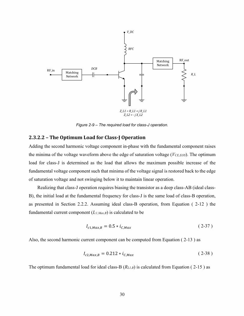
30
RF_in
V_DC
RF_out
RFC
MatchingNetwork
R_L
DCB
MatchingNetwork
Z_L1=R_L1+jR_L1Z_L2=‐jX_L2
Figure 2-9 – The required load for class-J operation.
2.3.2.2–TheOptimumLoadforClass‐JOperation
Adding the second harmonic voltage component in-phase with the fundamental component raises
the minima of the voltage waveform above the edge of saturation voltage (VCE,EOS). The optimum
load for class-J is determined as the load that allows the maximum possible increase of the
fundamental voltage component such that minima of the voltage signal is restored back to the edge
of saturation voltage and not swinging below it to maintain linear operation.
Realizing that class-J operation requires biasing the transistor as a deep class-AB (ideal class-
B), the initial load at the fundamental frequency for class-J is the same load of class-B operation,
as presented in Section 2.2.2. Assuming ideal class-B operation, from Equation ( 2-12 ) the
fundamental current component (Ic1,Max,B) is calculated to be
, , 0.5 ∗ , ( 2-37 )
Also, the second harmonic current component can be computed from Equation ( 2-13 ) as
, , 0.212 ∗ , ( 2-38 )
The optimum fundamental load for ideal class-B (RL1,B) is calculated from Equation ( 2-15 ) as

31
,, ,
, ,
,
0.5 ∗ ,
( 2-39 )
For class-J operation, the instantaneous collector voltage waveform that is constructed from
DC, fundamental, and second harmonic components can be written as
, , cos , cos 2 ( 2-40 )
where VDC is the DC supply voltage and assuming VCE,EOS = 0 to simplify the derivation. The Vce1,J
is the amplitude of the fundamental voltage component. The Vce2,J is the amplitude of the second
harmonic voltage component. The θ0 is the time-varying phase angle of the collector voltage which
is +π/4 out of phase with the collector current.
In order to determine the maximum increase of the fundamental load and the optimum reactive
termination for the second harmonic component while maintaining the minima of the voltage at
the edge of saturation voltage, Equation ( 2-40 ) is solved for the maximum value of Vce1,J with a
corresponding value of Vce2,J that causes the minima of the instantaneous collector voltage (vJ) to
equal zero, which corresponds to the edge of saturation voltage (VCE,EOS) in a real transistor.
At the minima of the waveform the slope equal to zero for a specified phase angle (θ0,Min).
Differentiating Equation ( 2-40 ) with respect to the phase angle (θ0)
, 0 , , 2 , 2 , ( 2-41 )
Applying the trigonometric feature sin(2θ) = 2 sin(θ).cos(θ)
,,
4 ,
( 2-42 )
Utilizing the feature cos(2θ)= 2 cos2(θ) – 1 and Equation ( 2-42 ) in Equation ( 2-40 )

32
, , 0 ,,
4 ,, 2 ,
4 ,
1
,
4 ,
,
8 ,,
,
8 ,,
( 2-43 )
Rearranging all terms and multiplying by Vce2,J
, ,,
80 ( 2-44 )
Solving Equation ( 2-44 ) for Vce2,J
,
4 ,8
2
( 2-45 )
For a real value of Vce2,J , the following equality must be valid
,
20 ( 2-46 )
which is rearranged to
, √2 ∗ ( 2-47 )
Therefore, the maximum value of the fundamental voltage component (Vce1,Max,J) can be given as
, , √2 ∗ ( 2-48 )
Applying that value of Vce1,Max,J in Equation ( 2-45 ), the corresponding value of the second
harmonic voltage component (Vce2,J) can be computed as

33
, 2 ( 2-49 )
By replacing VDC by the maximum amplitude of the fundamental voltage of class-B (Vce1,Max,B
= VDC – VCE,EOS) in Equations ( 2-48 ) and ( 2-49 ), we obtain
, , √2 ∗ , , ( 2-50 )
while the corresponding amplitude of the second harmonic voltage (Vce2,J) is found to be
, 0.5 ∗ , , ( 2-51 )
From Equation ( 2-36 ), the magnitude of the fundamental load of class-J operation is found to be
,, ,
, ,√2 ∗ , ( 2-52 )
Since class-J is biased as deep class-AB (ideal class-B), then Ic1,Max,J = Ic1,Max,B. From Equations (
2-50 ) and ( 2-52 )
√2 ∗ ,, ,
, ,
√2 ∗ , ,
, ,
√2 ∗ ,
( 2-53 )
Therefore, the resistive load at the fundamental component of class-J can be calculated as
, , ( 2-54 )
Calculating the reactive second harmonic termination of class-J
,,
, ,, ( 2-55 )

34
From Equation ( 2-37 ) and ( 2-38 ), The amplitude of the second harmonic current component can
be written in terms of the amplitude of the fundamental current component as
, ,0.2120.5 , , ( 2-56 )
From Equation ( 2-51 ) and ( 2-56 ) into Equation ( 2-55 )
,0.5 ∗ , ,
0.2120.5 , ,
1.179 ∗ , ,
, ,
1.179 ∗ ,
( 2-57 )
From Equations ( 2-54 ) and ( 2-57 ), the optimum load of class-J operation can be determined in
terms of the optimum fundamental load of class-B (RL1,B) operation as
, , ,
, 1.179 ∗ , ( 2-58 )
where the fundamental load of class-B operation can be easily calculated for a given transistor
from the I-V transfer characteristic which equals the optimum load of class-A. The optimum load
given in equation ( 2-58 ) agrees well with what have been proposed by other authors, such as
Wright, et al. [29], and Rezaei, et al. [30].
It is important to note that the proposed load of class-J is assumed to be presented at the output
current source of the transistor where the transistor parasitics and the output capacitance are
considered as part of the output matching network. In a real design, the load should be modified
to consider those effects.
2.3.2.3–MaximumLinearOutputPowerandPowerEfficiencyofClass‐J
Given that class-J operation is biased as ideal class-B, the optimum (maximum linear) output
power achieved by presenting the optimum load that is given by Equation ( 2-58 ) to the transistor
can be calculated by

35
,12 , , , , , , ( 2-59 )
where Ic1,Max,J = Ic1,Max,B. From the derivation of Section 2.2.3
, , 2∗ ( 2-60 )
From Equations ( 2-50 ) and ( 2-60 ) into Equation ( 2-59 ), and the phase difference between the
fundamental voltage and current components is +π/4 then cos(θv,1 – θi,1) = 1/√2 , the optimum
power of class-J can be calculated as
,12∗ √2 ∗ , , , , , ,
12∗ √2 , ∗
2∗ ∗
1
√2
4 ,
( 2-61 )
The corresponding maximum power efficiency is given by
,4 ,
( 2-62 )
where PL is the power delivered to the load (in Watts). The PDC is the consumed DC power (in
Watts). Assuming an ideal transistor where VCE,EOS is very small and approaching a value of zero,
then the efficiency for an ideal transistor (ηideal,J) is given by
,4 78.5% ( 2-63 )
It should be noted that both the optimum (maximum linear) output power and the power efficiency
of class-J match the ideal class-B operation.

36
2.3.3–Class‐FOperation
Class-F is another concept of utilizing the generated harmonics to improve the power efficiency
of the power amplifier, as presented by Raab [31]. In class-F, the third harmonic voltage
component is utilized to engineer the collector/drain voltage. Aiming at achieving the same goal
of utilizing the harmonics, adding the third harmonic voltage component to the fundamental
component reduces the peak-to-peak voltage swing of the resultant waveform, as shown in Figure
2-10. The resultant voltage waveform has a higher minima than a sinusoid at the fundamental
frequency, allowing the increase of the fundamental voltage component by increasing the load
impedance magnitude at the fundamental frequency. As a result, the fundamental output power
increases with no increase in the DC power, which transfers into an increase of the power
efficiency.
Figure 2-10 – Class-F voltage waveform - The effect of adding a third harmonic voltage component to the
fundamental component (normalized to (VDC - VCE,EOS), the zero value refers to VCE,EOS).
In class-F operation, the transistor is typically biased as class-AB. It is interesting to note that
the third harmonic current component at the ideal class-B operation equal to zero, as shown in
Figure 2-4. Therefore, in class-F, the real transistor is typically biased more towards class-AB
operation to generate a moderate level of the third harmonic. Such a biasing condition results in a
high level of the second harmonic current component. Hence, the optimum class-F operation
mandates presenting a short-circuit termination at the second harmonic.

37
2.4–Summary
This chapter presented the current techniques of improving the power efficiency of a linear power
amplifier, deep class-AB and class-F. The main issue that hinders these techniques from achieving
the maximum theoretical power efficiency lies in the implementation part of the design. In deep
class-AB operation, presenting a non-perfect short-circuit at the harmonics, especially the second
harmonic, by using a small shunt capacitor at the collector terminal rather than a second harmonic
trap or using a single second-harmonic trap rather than double second-harmonic traps in a
broadband design, causes degradations in both power efficiency and output power.
Class-J operation was investigated in details where the optimum load, the maximum power
efficiency, and the maximum linear output power were calculated. The analysis of class-J was
restricted to utilizing the second harmonic voltage component rather than the general theoretical
definition of class-J where the second and higher harmonic voltage components can be utilized.
Class-J has few advantages that makes it suitable to the implementation of a handset power
amplifier. Class-J does not require a perfect short-circuit termination to the second harmonic,
eliminating the need for a second harmonic trap and avoiding the implementation issue of deep
class-AB. Class-J adds the second harmonic voltage component with the right phase to the
fundamental component which increases the minima of the voltage waveform away from the edge
of saturation voltage (VCE,EOS) avoiding the operation in the saturation region of the transistor
which is a highly non-linear region. Therefore, class-J can achieve a higher practical power
efficiency than deep class-AB while maintaining a high linearity.
While this chapter focused on techniques to achieve high power efficiency, the next chapter
discusses the linear operation of power amplifiers, where the sources of nonlinearity and the
techniques to improve the linear operation are presented.

38
Appendix
A2.1–DerivationoftheCollectorCurrentComponents
The collector current waveform takes the shape of a truncated sinusoid when operating at a reduced
conduction angle, as shown in Figure 2-11.
Figure 2-11 – The collector current waveform as a truncated sinusoid (normalized to maximum current).
Following the analysis presented by Cripps [10], the instantaneous collector current (iC), as a
function of the angle variable (θ = ω t), is represented as,
, cos ,2 2
0,2
,2
( 2-64 )
where,
, , ( 2-65 )
and IDC,Q is the quiescent DC collector current. The iC,Max is the maximum instantaneous collector
current for the given transistor. The α is the conduction angle.
Noting that at θ = (α / 2), iC = 0, and substituting into Equation ( 2-64 ),

39
, cos2
( 2-66 )
Utilizing Equation ( 2-65 ) results in,
, , , . cos2
( 2-67 )
Rearranging both sides of the equation,
, cos2 , cos
21 ( 2-68 )
Then IDC,Q can be written as,
, ,
cos 2cos 2 1
( 2-69 )
Also, from Equation ( 2-66 ),
,
cos 2
( 2-70 )
Substituting from Equation ( 2-69 ), then Ic can be written as,
,1
cos 2 1 ( 2-71 )
Substituting from Equations ( 2-69 ) and ( 2-71 ) into Equation ( 2-64 ), in order to write the
instantaneous collector current (iC) in terms of iC,Max and α ,

40
,
cos 2cos 2 1
,cos
cos 2 1,
2 2
0,2
,2
,
cos 2 1cos
2cos ,
2 2
0,2
,2
( 2-72 )
Performing the Fourier series analysis, while considering:
Since it was elected to represent the collector current waveform in terms of a cosine
function which is an even function, only the even exponents of the Fourier coefficients
exist.
Typically, the integrals of the Fourier series are performed in the time-domain. But the
integrals can be transformed to the angle-domain by considering, θ = ω.t , then dθ =
ω.dt .
From the Fourier series analysis, the DC component is calculated by,
12
. ( 2-73 )
Solving Equation ( 2-73 ), and utilizing the trigonometric feature ( sin(-x) = -sin(x) ), the DC
collector current component is given as,
12
. ,
cos 2 1. cos
22 sin
2 ( 2-74 )
From the Fourier series analysis, the harmonic components are calculated by,
1 . cos . ( 2-75 )

41
where n is the harmonic component index. Solving Equation ( 2-75 ), and employing the
trigonometric features: (cos(a).cos(b) = (1/2).(cos(a+b) + cos(a-b))), and ( sin(-x) = -sin(x) ).
1. ,
cos 2 1.2cos
2sin
211sin 1
2
11sin 1
2
( 2-76 )
Simplifying Equation ( 2-76 ) by using the feature (sin(a).cos(b) = (1/2).(sin(a+b) + sin(a-b))),
1. ,
cos 2 1.1sin 1
21sin 1
2
11sin 1
211sin 1
2
1. ,
cos 2 1.
1 11sin 1
2
1 11sin 1
2
( 2-77 )
Applying (n = 1) in Equation ( 2-77 ) and utilizing the feature ( Limx→0 (sin(x)/x) = 1 ), the
fundamental collector current component is computed as,
1. ,
cos 2 1.12sin
2 ( 2-78 )
Applying (n = 2) in Equation ( 2-77 ), the second harmonic current component is given as,
1. ,
cos 2 1.16sin
32
12sin
2 ( 2-79 )

42
Applying (n = 3) in Equation ( 2-77 ), the third harmonic current component is calculated as,
1. ,
cos 2 1.112
sin 216sin ( 2-80 )

43
3.
LinearityinRFPowerAmplifiersandBiasCircuits
3.1–Introduction
A linear time-invariant circuit must hold the superposition concept and not generate new
frequencies. For a transistor that operates as a transconductance amplifier, an ideal linear amplifier
can be defined by the relationship between the input and output signals as follows
. ( 3-1 )
where vi is the input voltage signal. The io is the output current signal. The gm is the amplifier
transconductance, where gm is a constant.
Typically, weakly nonlinear operation of the power amplifier is modeled using a power series,
or a Volterra series where the phase effect is included. The coefficients of the series are function
of the bias point of the transistor as well as the output and input matching networks.
. . . ⋯ ( 3-2 )
A circuit that operates under a strong nonlinearity is best analyzed using a harmonic-balance
or a time-domain approach. However, it is still desirable to develop a basic understanding of the
analysis independent of the simulation when using CAD tools.
The nonlinear operation of the power amplifier causes the generation of unwanted distortion
products which extend out of the intended channel of the transmitted signal. The unwanted
distortion products may interfere with signals in other channels. Therefore, it is necessary to reduce
their level. In the case of applying an unmodulated two-tone signal, the distortion products can be
categorized into harmonic components and intermodulation distortion (IMD) products. The
harmonic components and the even-order intermodulation products can be easily filtered out by a
low-pass filter and appropriate DC-blocks. Odd-order intermodulation products, especially third,
fifth, and seventh which occur in-band, in adjacent channels, and alternate adjacent channels, are
almost impossible to attenuate due to their existence close to the intended channel.

44
Recent cellular standards employ linear modulation schemes where both the amplitude and
phase of the transmitted signal contain information that is required to be preserved during
transmission. A major purpose of employing a linear modulation scheme is to achieve a higher
spectrum efficiency. For example, Long-Term Evolution (LTE) and LTE-Advanced employ
Quadrature Phase Shift Keying (QPSK), and Quadrature Amplitude Modulation (16-QAM, and
64-QAM). In order to achieve a high data-rate, current standards (LTE, and LTE-Advanced) utilize
Orthogonal Frequency-Division Multiplex (OFDM) as a multi-carrier modulation format.
Different access schemes are applied in the downlink and uplink. In the downlink, Orthogonal
Frequency-Division Multiple Access (OFDMA) is used, which is a multi-carrier access scheme,
but has the disadvantage of a high peak-to-average power ratio (PAPR). In order to improve the
handset power efficiency, in the up-link Single-Carrier - Frequency-Division Multiple Access (SC-
FDMA) is utilized since it has a lower peak-to-average power ratio.
The requirement for linearity in radio-frequency power amplifiers arises from the necessity of
achieving minimum interference with other channels in the frequency spectrum. Also, as cellular
standards apply digital modulation schemes with both of the amplitude and phase are varying, the
need for linear power amplifiers increases, since the nonlinearity of the power amplifier causes not
only a spectral spreading, but also amplitude and phase distortions of the transmitted signal.
3.2–NonlinearitiesinPowerAmplifiers
3.2.1–TheNatureofNonlinearities
In power amplifiers, as the input drive signal increases the output power (Pout) increases until it
reaches the 1dB compression point. Increasing the input power further causes the output power to
approach a saturated power level as shown in Figure 3-1. In terms of sweeping the input power
(Pin), the power amplifier operation can be divided into two regions: the varying output power
region and the saturated output power region. In Figure 3-1, the varying output power region is the
region below Pout = 32 dBm, while the saturated output power region is the region above Pout = 32
dBm.

45
Figure 3-1 – Output power (Pout) vs. input power (Pin), and power gain (GP) vs. output power (Pout) as input
power (Pin) is swept.
3.2.1.1–WeakandStrongNonlinearities
The nature of nonlinearity is different in each of the regions defined in Figure 3-1. The transistor
nonlinear I-V transfer characteristics can be categorized into a weak nonlinearity and a strong
nonlinearity, Maas [9]. In the saturated output power region, the strong nonlinearity occurs as the
power amplifier operates beyond the 1 dB compression point, where the input drive is large such
that the collector current and voltage waveforms exceed the boundaries of saturation and cut-off.
-15 -10 -5 0 5 10-20 15
15
20
25
30
10
35
Pin (dBm)
Pout vs. Pin
15 20 25 3010 35
20
22
24
26
28
30
18
32
Pout (dBm)
G_P vs. Pout

46
The varying output power region coincides with the continuous region of the I-V transfer
characteristics, where the weak nonlinearity occurs. An example is the operation of a class-A
power amplifier up to, but not beyond, the 1 dB compression point. It should be noted, when
operating at a reduced conduction angle, the truncated sinusoid of the collector current becomes
another source of nonlinearity.
For a constant envelope signal, it is desirable to operate the power amplifier at the saturated
output power level (Pout = 34 dBm, in Figure 3-1), to achieve the highest possible efficiency.
Hence, the power transistor shows a strongly nonlinear behavior as high levels of harmonic
components and intermodulation distortion products are generated. In contrast, for a signal with a
varying envelope, the amplifier operates within the power range of the signal such that the
maximum power of that range coincides with the maximum linear power of the varying output
power region (Pout = 32 dBm, in Figure 3-1). In that case, the power transistor shows a weakly
nonlinear behavior as low levels of harmonic components and intermodulation distortion products
are produced.
3.2.1.2–AM‐AMandAM‐PMConversions
An ideal linear power amplifier is expected to have a constant power gain (GP) (constant AM-AM
conversion), in the varying output power region.9 Increasing the input power by 1dB should
increase the output power by 1dB. But, in general, the varying output power region may show a
constant power gain, a gain compression, or a gain expansion.10 Both gain compression and gain
expansion present a form of an undesired AM-AM distortion.
Phase distortion is an important aspect of the nonlinear operation of the power amplifier. Both
amplitude distortion and phase distortion cause a waveform distortion. It is often observed that as
the output power level varies, the phase difference between the output and input signals varies, in
what is known as AM-PM conversion.11 Such a situation is related to the nonlinear characteristics
of the power transistor, Jardon A and Vazquez L [32] and Cabral, et al. [33]. Ideally, a linear power
amplifier is expected to have a constant phase difference over the varying output power region.
9 - The term “AM-AM” refers to the process of varying the input power causes a variation in the output power. 10 - Gain expansion refers to the phenomenon where increasing the input power causes the power gain to increase before the output power approaches the compression then the saturated power level. 11 - The term “AM-PM” refers to the process where varying the output power, by sweeping the input power, causes the phase difference to vary.

47
3.2.1.3–TheReducedConductionAngleEffect
Cripps [10] has presented a detailed analysis for the reduced conduction angle operation using a
transistor with an ideal I-V transfer characteristics as it operates with a linear transconductance and
a zero value for the edge of saturation voltage (VEOS). The results of the analysis show that AM-
AM linear operation is a function of the conduction angle. The analysis illustrates this aspect in
terms of the classical power amplifier classes. A class-A power amplifier has a constant gain due
to the assumption of the linear transconductance. A class-AB operates with a gain compression
(nonlinear AM-AM) with the existence of odd-order harmonic components generated by the
truncated sinusoid of the collector current. A class-B operates with a constant gain (linear AM-
AM) with no odd-order harmonic components. While a class-C shows a gain expansion (nonlinear
AM-AM). As a conclusion, operating at a reduced conduction angle inherits a nonlinearity that is
a function of the conduction angle value due to the truncated sinusoid of the collector current.
3.2.2–TheTransistorEffectonLinearity
3.2.2.1–TheHBTTransistorEffect
The analysis discussed in Section 3.2.1.3 assumes an ideal transistor with a linear transconductance
but, an HBT transistor is governed by the exponential relationship between the base-emitter
voltage (vBE) and the collector current (iC). As a result, the HBT transistor exhibits a smooth
transition between the cut-off and active regions. Hence, the ideal class-B definition is not
applicable to such a transistor, since there is no specific bias point where the transistor turns on.
The exponential relationship of the HBT transistor displays an expansive transconductance
within the varying output power region. As the input power increases, the transconductance
increases which is a result of the DC bias changes. The transistor transconductance is given by
( 3-3 )
Additionally, the HBT transistor shows a varying nonlinear input impedance, as it contains both
nonlinear input capacitance and resistance at the base-emitter PN junction, Woonyun, et al. [34].
An investigation was carried out on an HBT transistor to recognize the effect of reducing the
conduction angle on the linear operation within the varying output power region. Figure 3-2 shows

48
the simulation results of the power gain (GP) as the input power (Pin) increases. A specific base
bias voltage was found where a constant gain is maintained and the power amplifier operates as a
linear amplifier at the fundamental frequency. This operation refers to the deep class-AB,12 which
is equivalent to the ideal class-B operation. As the base bias voltage increases above that bias point,
causing the conduction angle to increase, the power amplifier displays a gain compression. Which
refers to a quasi-AB operation. But as the bias voltage decreases below the deep class-AB bias
point, the conduction angle decreases and a gain expansion is observed. This smaller conduction
angle case refers to class-C operation.
Figure 3-2 – The effect of bias point and reduced conduction angle on linearity.
It is interesting to observe that a real HBT transistor displays a better linear operation than an
ideal piece-wise linear device when in deep class-AB operation. An explanation of such a better
linearity is a cancellation takes place between the gain compression (due to nonlinearity of the
truncated sinusoid) and the expansive transconductance occurring due to the device exponential
relationship.
3.2.2.2–Odd‐DegreeComponentsEffect
Cripps [11] has revealed that a specifically engineered nonlinearity of a transistor may help to
improve both of the linearity and efficiency of the power amplifier when operating at a reduced
12 - The term deep class-AB refers to the operation with a conduction angle less than but very close to 180 where a specific low bias point provides a linear AM-AM operation.

49
conduction angle. The transistor is assumed to exhibit a nonlinear transconductance that only
produces the fundamental and even-harmonic current components. Although such a device does
not exist, the analysis provides a conceptual understanding that a real device may show a linear
operation and higher efficiency than an ideal device. Also, the analysis shows that eliminating the
odd-order harmonic components helps achieving a better linearity. It should be noted that the
highlighted analysis agrees with the discussion of Section 3.2.13 where an ideal class-B is highly
linear as it contains no odd-order harmonic components.
3.2.3–HBTDesignConsiderations
3.2.3.1–SimpleHBTLarge‐SignalModel
A simple large-signal model for an HBT transistor that operates in the active region is shown in
Figure 3-3. The model contains a base-emitter diode and a collector-emitter current source. The
model represent a simplified version of the Ebers-Moll model for a bipolar transistor, Gray [35].
Although the model is much simpler than an advanced full model of HBT transistor, Zhang, et al.
[36], both agree in the fundamental function that describe the power amplifier operation.
B C
E
g_m.v_be+v_be‐
Figure 3-3 – A simplified HBT large-signal model for operation in the active region.
The following two equations governs the relationship between the collector current (iC), the
base current (iB), and the base-emitter voltage (vBE)
( 3-4 )
1 ( 3-5 )
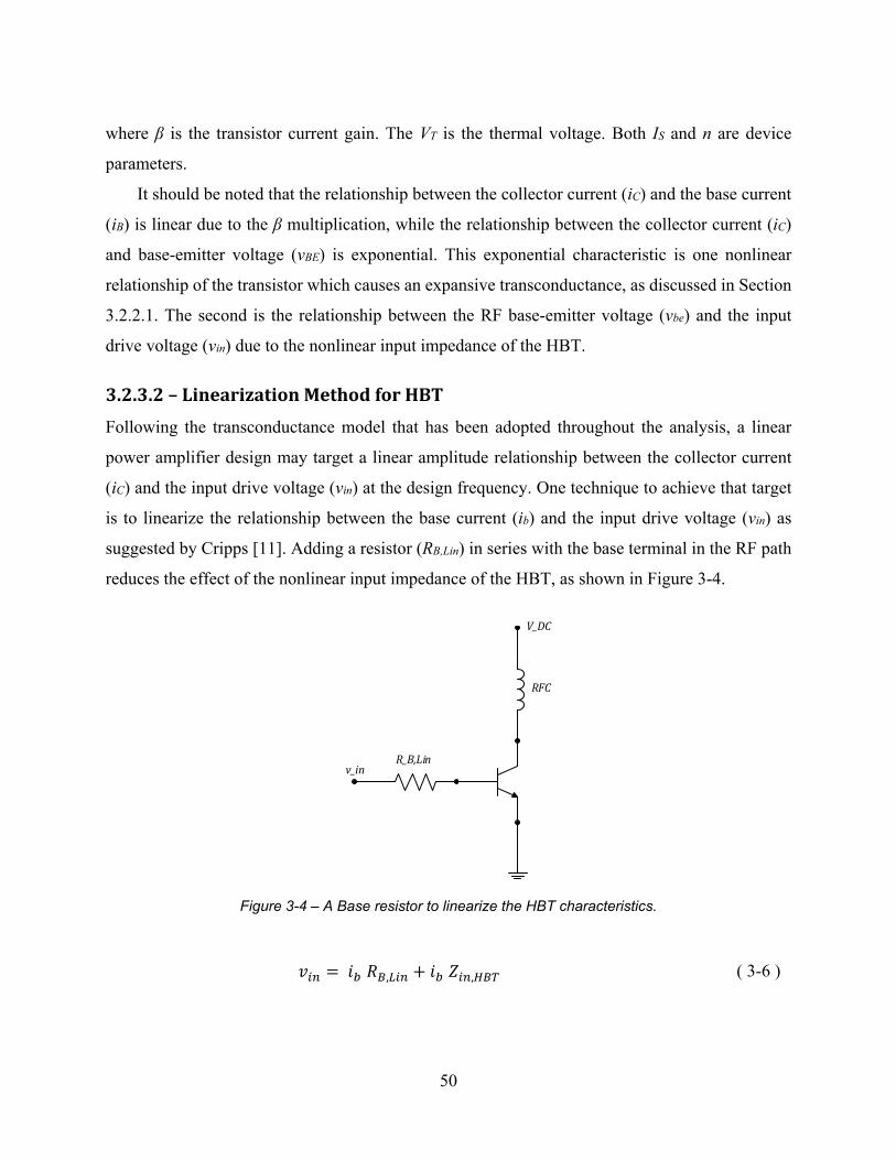
50
where β is the transistor current gain. The VT is the thermal voltage. Both IS and n are device
parameters.
It should be noted that the relationship between the collector current (iC) and the base current
(iB) is linear due to the β multiplication, while the relationship between the collector current (iC)
and base-emitter voltage (vBE) is exponential. This exponential characteristic is one nonlinear
relationship of the transistor which causes an expansive transconductance, as discussed in Section
3.2.2.1. The second is the relationship between the RF base-emitter voltage (vbe) and the input
drive voltage (vin) due to the nonlinear input impedance of the HBT.
3.2.3.2–LinearizationMethodforHBT
Following the transconductance model that has been adopted throughout the analysis, a linear
power amplifier design may target a linear amplitude relationship between the collector current
(iC) and the input drive voltage (vin) at the design frequency. One technique to achieve that target
is to linearize the relationship between the base current (ib) and the input drive voltage (vin) as
suggested by Cripps [11]. Adding a resistor (RB,Lin) in series with the base terminal in the RF path
reduces the effect of the nonlinear input impedance of the HBT, as shown in Figure 3-4.
R_B,Lin
V_DC
RFC
v_in
Figure 3-4 – A Base resistor to linearize the HBT characteristics.
, , ( 3-6 )

51
where Zin,HBT represents the nonlinear input impedance of the HBT transistor. As RB,Lin increases
such that RB,Lin >> Zin,HBT, the term (iB. RB,Lin) dominates the right hand side. Since RB,Lin is a linear
resistor, the relationship between the input drive voltage (vin) and the RF base current (ib) becomes
more linear. This modification can be seen as linearizing the performance of the transistor from
the exponential relationship in Equation ( 3-5 ) towards a linear relationship between the input
voltage (vin) and the RF base current (ib).
3.2.3.3–InputMatchingNetworkEffect
The input matching network is often designed to be of a high Q. As a result, the harmonic
components of the base current see a different impedance than the fundamental. The matching
network frequency response shapes the base current and causes the same effects to the collector
current waveform.
Utilizing the reduced conduction angle technique aims at obtaining a collector current
waveform of a truncated sinusoid which contains many harmonic components, while retaining a
linearity at the fundamental frequency. Since the relationship between the base current (iB) and the
collector current (iC) is linear, the same shape of the truncated sinusoid for the base current is
obtained for both waveforms. In order for the linearizing resistor (RB,Lin) to be effective in
improving the linearity, the resistor must be a real resistor and not be applied to the base terminal
through a transformation of the input matching network. Hence, the input matching network has a
key effect on linearity in HBT-based power amplifiers and must be considered in the design.
3.2.3.4–BiasResistorEffect
A disadvantage of adding a real resistor in the RF path, as discussed in the last Section 3.2.3.2, is
the decrease in the power gain which may cause a degradation in the power added efficiency
(PAE). Typically, the bias circuit is also connected to the base of the power transistor through a
bias resistor (RB,Bs), as shown in Figure 3-5, which increases the output impedance of the bias
circuit and acts as an RF choke to reduce the RF leakage to the circuit.
The bias resistor can be utilized to improve the linear operation without adding a real resistor
in the RF path since both the output (Thevenin) impedance of the input matching network (Zout,IMN)
and the output impedance of the bias circuit (Zout,Bs) define the impedance presented to the base of
the power transistor. Figure 3-6 highlights that concept, as it shows the equivalent circuit of the
circuit shown in Figure 3-5, by considering the input matching network presents the required
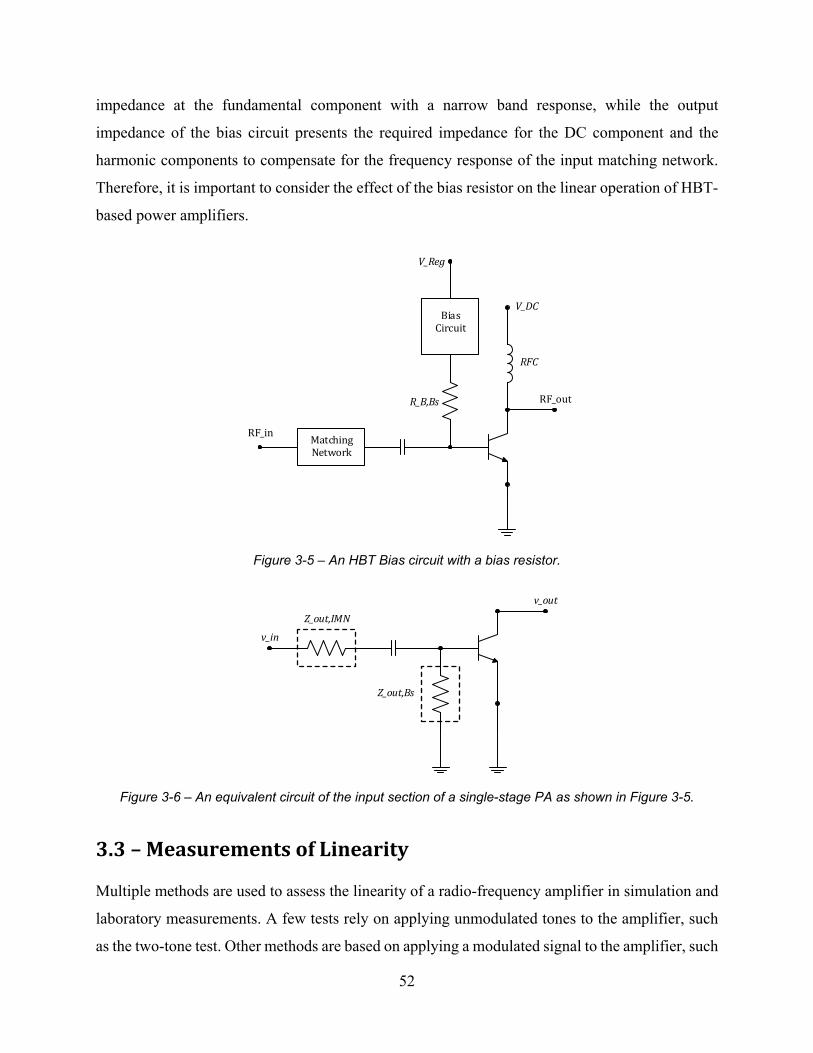
52
impedance at the fundamental component with a narrow band response, while the output
impedance of the bias circuit presents the required impedance for the DC component and the
harmonic components to compensate for the frequency response of the input matching network.
Therefore, it is important to consider the effect of the bias resistor on the linear operation of HBT-
based power amplifiers.
R_B,Bs
RF_inMatchingNetwork
V_DC
RF_out
RFC
V_Reg
BiasCircuit
Figure 3-5 – An HBT Bias circuit with a bias resistor.
v_in
v_out
Z_out,Bs
Z_out,IMN
Figure 3-6 – An equivalent circuit of the input section of a single-stage PA as shown in Figure 3-5.
3.3–MeasurementsofLinearity
Multiple methods are used to assess the linearity of a radio-frequency amplifier in simulation and
laboratory measurements. A few tests rely on applying unmodulated tones to the amplifier, such
as the two-tone test. Other methods are based on applying a modulated signal to the amplifier, such

53
as adjacent channel power ratio (ACPR) and error vector magnitude (EVM) measurements. Those
tests also provide an indication of the memory effect occurring in the power amplifier.
3.3.1–Two‐toneTest
The two-tone test is one method of evaluating the linearity of the amplifier. The test applies two
unmodulated tones (at frequencies: f1 and f2) within the intended channel. Both tones have the
same power level, as shown in Figure 3-7. The idea of applying two tones is to modulate the
envelope of the input signal across its full range.
Figure 3-7 – Spectrum of the two-tone signal, the generated IMDs and harmonics.
Due to the nonlinearity of the amplifier, harmonic distortion components and intermodulation
distortion products of all orders are generated. Harmonic components (2f1, 2f2, 3f1, 3f2 …) are
easily rejected by adding a low pass filter following the amplifier, or constructing the output
matching network of the amplifier to have a frequency response of a low-pass filter form. All
orders of intermodulation distortion products are generated. In general, the frequency of the
intermodulation products are given by
( 3-7 )
where m and n are integers. Odd-order intermodulation products that appear in-band, and within
the adjacent channels and the alternate adjacent channels, are of great concern since it is extremely
difficult to reject them. The main focus is on the third-order products ((2f1 – f2) and (2f2 - f1)) since

54
they usually have the highest level of all intermodulation products and are the closest to the
intended channel.
Multiple parameters are calculated from the generated distortion products to evaluate the
linearity, such as the second-order intercept point (IP2), the third-order intercept point (IP3), and
the intermodulation distortion ratio (IMR), Kenington [37].
It should be noted that, if the two-tone test results in an unequal power level of the
intermodulation products on each side of the intended channel, then that is an indication of the
memory effect occurring in the amplifier.
3.3.2–AdjacentChannelPowerRatio(ACPR)
The adjacent channel power ratio is a test to evaluate the linearity of the amplifier when it is driven
by a modulated signal. It is a measure of the spectral spreading in the adjacent channels and
alternate adjacent channels. Typically, the input signal to the amplifier has spectral components
that are only contained in the intended channel. The nonlinearity of the amplifier causes a spectral
spreading out of the intended channel to the adjacent channels. The adjacent channel power ratio
is defined as the ratio of the power of a specified bandwidth (BW2), which is centered at an offset
from the center of the main channel, to the power of a specified bandwidth (BW1), which is
centered within the main channel, as shown in Figure 3-8. In general, both bandwidths (BW1 and
BW2) are not equal and each bandwidth may represent a specified bandwidth of a channel that is
determined by the industry standards, [3GPP [38], 39, 40].
Figure 3-8 – Adjacent channel power ratio (ACPR).

55
An indication of the memory effect in power amplifiers is to compare the spectral spreading
level on each side of the main channel. A difference is indicative of a memory effect existence.
Tests of linearity, which are based on applying a modulated input signal, require more
advanced measurement equipment in the laboratory and advanced simulation techniques which
consume longer simulation times compared to the two-tone test. One approach is to use the results
of the two-tone test to obtain approximated results for the ACPR test. Such an approach for the
adjacent channel power ratio was presented by Borges de Carvalho and Pedro [41]. It should be
noted that the approach is considered a quick and easy estimate that has some expected inaccuracy,
but provides a simple method to obtaining the desired data.
3.3.3–ErrorVectorMagnitude(EVM)
The error vector magnitude is another test to assess the linearity of the amplifier when it is driven
by a modulated signal. It is a measure of the signal waveform distortion due to the amplitude and
phase distortions that occur within the amplifier. The same test is also applied to evaluate the
distortion within the transmission link between a transmitter and a receiver.
The error vector magnitude test is carried out by measuring the difference between the
reference waveform and the measured waveform. In the I-Q plane, the difference in amplitude and
phase between the ideal constellation point (reference symbol) and the measured point (measured
symbol) called the error vector. The error vector magnitude is defined, in dB, as the ratio of the
mean power of the error vector to the mean power of the reference vector. It is also defined, in
percentage, as the square root of the ratio of the mean power of the error vector to the mean power
of the reference vector, [3GPP [38], 39, 40].
3.4–HBTBiasCircuits
The bias circuit is an important element that influences the power amplifier performance. It was
shown, in Section 3.2.2.1, that the bias point should be selected carefully to achieve the needed
linear operation as well as a high power efficiency.
The bias circuit is required not only to provide a specific current/voltage to the power
transistor, but also to compensate for a multiple of variations. As the power amplifier operates,
power dissipation occurs, raising the temperature of the power transistor and the circuit elements
surrounding it. The bias circuit is required to compensate for such temperature variations as well
56
as the temperature variation due to the environment. During production, process variations are
observed among different wafers, different lots of wafers, and on the same wafer among dies from
the center of the wafer to the edge of the wafer. Hence, the design of the bias circuit should also
be robust against process variations.
Another factor that should be considered during the design of the bias circuit is the RF leakage
to the circuit from the RF path. In integrated circuits, utilizing an on-chip inductor as an RF choke
between the bias circuit and the base of the power transistor is not preferred. Inductive chokes
contradict the requirement of a compact die size. As a result, the bias circuit is usually connected
through a resistor to the base of the power transistor where the RF signal is applied, causing an RF
leakage to the bias circuit which may affect the amplifier performance.
Typically, two DC supply voltages are available for a power amplifier module in handsets.
One is supplied by a regulated DC-DC converter (VDC) which is typically connected to the collector
of the power transistor through an RF choke. The other is supplied from the battery (VBatt) which
varies over a wide voltage range (3 V - 4.8 V). Within the power amplifier module, a controller
provides a regulated voltage (VReg) from the unregulated battery supply to serve as the
reference/supply voltage for the bias circuits in order to maintain a constant circuit performance
across the wide voltage range of the battery. Typically, the regulated voltage has the disadvantage
of low current driving capability.
This section presents a few bias circuits that are used in handset power amplifiers, starting
from basic circuits and ending with circuits that provide temperature compensations as well as a
reduction of the bias offset at high drive levels to improve linearity.
3.4.1–BasicBiasCircuits
In a class-A power amplifier, the bias circuit aims to establish a constant DC collector current that
is insensitive to variations in temperature and process. One basic approach for biasing the power
transistor is to apply a fixed base voltage, by directly connecting the regulated voltage (VReg) to the
base of the power transistor. Another approach is to supply a fixed base current, by connecting the
regulated voltage to the base of the power transistor through a resistor, as shown in Figure 3-9.
Both approaches have major disadvantages and alternatives are recommended. In either case, the
power transistor may require a large DC base current at high output power levels, which may
interfere with the low current driving capability of the regulated supply voltage. In the case of
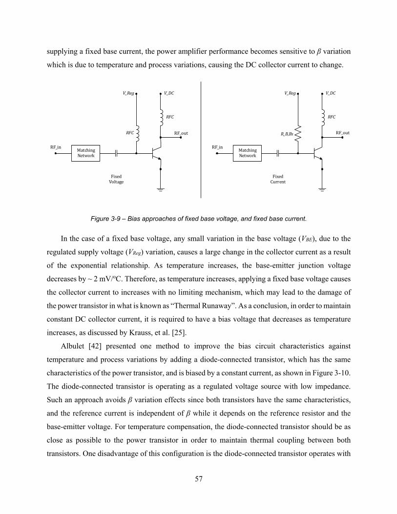
57
supplying a fixed base current, the power amplifier performance becomes sensitive to β variation
which is due to temperature and process variations, causing the DC collector current to change.
FixedVoltage
FixedCurrent
R_B,Bs
RF_in
V_DCV_Reg
RF_out
RFC
MatchingNetwork
RF_in
V_DCV_Reg
RF_out
RFC
MatchingNetwork
RFC
Figure 3-9 – Bias approaches of fixed base voltage, and fixed base current.
In the case of a fixed base voltage, any small variation in the base voltage (VBE), due to the
regulated supply voltage (VReg) variation, causes a large change in the collector current as a result
of the exponential relationship. As temperature increases, the base-emitter junction voltage
decreases by ~ 2 mV/oC. Therefore, as temperature increases, applying a fixed base voltage causes
the collector current to increases with no limiting mechanism, which may lead to the damage of
the power transistor in what is known as “Thermal Runaway”. As a conclusion, in order to maintain
constant DC collector current, it is required to have a bias voltage that decreases as temperature
increases, as discussed by Krauss, et al. [25].
Albulet [42] presented one method to improve the bias circuit characteristics against
temperature and process variations by adding a diode-connected transistor, which has the same
characteristics of the power transistor, and is biased by a constant current, as shown in Figure 3-10.
The diode-connected transistor is operating as a regulated voltage source with low impedance.
Such an approach avoids β variation effects since both transistors have the same characteristics,
and the reference current is independent of β while it depends on the reference resistor and the
base-emitter voltage. For temperature compensation, the diode-connected transistor should be as
close as possible to the power transistor in order to maintain thermal coupling between both
transistors. One disadvantage of this configuration is the diode-connected transistor operates with

58
a high bias current that is proportional to the collector current of the power transistor, mandating
it to be large and causing it to consume high DC power which reduces the overall efficiency of the
power amplifier. Also, this configuration does not provide a solution to the issue of the limited
current of the regulated supply voltage (VReg).
R_B,Bs
RF_in
V_DC
V_Reg
R_Ref
RF_out
RFC
MatchingNetwork
Figure 3-10 – A bias circuit of a single diode-connected transistor.
3.4.2–EnhancedBiasCircuits
Figure 3-11 shows a modified circuit of the single-diode bias circuit shown in Figure 3-10,
presented by Matilainen, et al. [43]. Adding a base-current drive transistor to the diode-connected
transistor and connecting its collector to the unregulated supply voltage (VBatt) reduces the required
current from the regulated supply (VReg) by shifting the majority of the required current to the
unregulated battery supply. The modification of the circuit causes no effect on the performance
since the regulated voltage is typically lower than the lowest level of the battery voltage. In the
modified circuit, the temperature compensation mechanism is the same as the single-diode circuit.

59
R_B,Bs
RF_in
V_DC
V_Reg
R_Ref
RF_out
V_Batt
RFC
MatchingNetwork
Figure 3-11 – A bias circuit of a modified single-diode circuit with a base-current driver.
Another improved bias circuit, that was discussed by Krauss, et al. [25], provides a solution
to the issue of the low-current driving capability of the regulated supply voltage (VReg), as shown
in Figure 3-12. Adding an emitter follower to the single-diode bias circuit, reduces the current
needed from the regulated supply voltage, since the collector of the emitter follower is connected
to the unregulated battery voltage (VBatt), where most of the current is supplied. For the circuit to
operate properly, another diode-connected transistor is stacked in the reference branch. The
double-diode configuration provides a temperature compensation in the same manner as the single-
diode configuration with the requirement of the double diodes being in close proximity with the
power transistor to maintain a good thermal coupling. One disadvantage of this configuration is
the limited voltage difference available to the reference resistor, since an HBT transistor usually
exhibits a base-emitter voltage of 1.15 V, requiring a high battery supply voltage and causing the
circuit to be sensitive to variations of the regulated supply voltage.
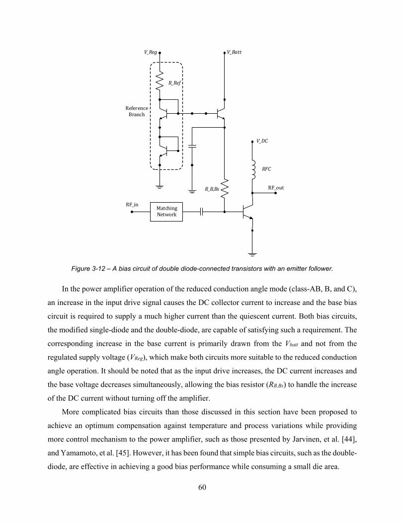
60
R_B,Bs
RF_in
V_DC
V_Reg
R_Ref
RF_out
V_Batt
RFC
MatchingNetwork
ReferenceBranch
Figure 3-12 – A bias circuit of double diode-connected transistors with an emitter follower.
In the power amplifier operation of the reduced conduction angle mode (class-AB, B, and C),
an increase in the input drive signal causes the DC collector current to increase and the base bias
circuit is required to supply a much higher current than the quiescent current. Both bias circuits,
the modified single-diode and the double-diode, are capable of satisfying such a requirement. The
corresponding increase in the base current is primarily drawn from the Vbatt and not from the
regulated supply voltage (VReg), which make both circuits more suitable to the reduced conduction
angle operation. It should be noted that as the input drive increases, the DC current increases and
the base voltage decreases simultaneously, allowing the bias resistor (RB,Bs) to handle the increase
of the DC current without turning off the amplifier.
More complicated bias circuits than those discussed in this section have been proposed to
achieve an optimum compensation against temperature and process variations while providing
more control mechanism to the power amplifier, such as those presented by Jarvinen, et al. [44],
and Yamamoto, et al. [45]. However, it has been found that simple bias circuits, such as the double-
diode, are effective in achieving a good bias performance while consuming a small die area.

61
3.5–HBTBiasConsiderations
3.5.1–BiasDepression
A bias depression phenomenon is observed in power amplifiers that employ HBT power
transistors, particularly at high input drive levels. An increase in the input drive signal causes a
decrease in the base-emitter DC voltage (VBE), as it shifts from the idle case where no input drive
signal is applied. In general, the bias depression occurs when applying an RF input drive signal to
a nonlinear load through a capacitive coupling. The nonlinear load may represent the base-emitter
PN junction of the HBT transistor, while the capacitive coupling is typically due to the DC
blocking capacitor that is used at the base of the power transistor, as shown in Figure 3-13.
R_B,Bs
RF_inMatchingNetwork
V_DC
RF_out
RFC
V_Reg
BiasCircuit
Figure 3-13 – An HBT with DC blocking capacitor and a bias circuit.
Clarke and Hess [15] have presented a detailed analysis for the case where an RF drive source
is coupled to a nonlinear load through a capacitor. Following their analysis to gain a deeper
understanding of the cause of the bias depression phenomenon, which may be seen as a basic
rectification process. The input of a single-stage power amplifier, as shown in Figure 3-13, can be
simplified to the circuit shown in Figure 3-14. In the figure, the diode (nonlinear load) represents
the base-emitter PN junction. The RF voltage source represents the RF input drive signal. While,
the DC current source represents the DC base current supplied from the bias circuit.

62
+v_D‐
+v_in(t)‐
I_DC
+V_C‐
Figure 3-14 – An RF drive signal is coupled to a nonlinear load through a capacitor.
From the circuit, the instantaneous input current signal (iIN) can be written as
( 3-8 )
where iD is the diode instantaneous current and vD is the diode instantaneous voltage. The VT is the
thermal voltage which is given by
( 3-9 )
Assuming the DC blocking capacitor is a short circuit at RF frequencies, then VC = - VD,DC , where
VD,DC is the diode DC voltage. Therefore
, ( 3-10 )
Assuming the input drive signal vIN(t) = V1 . cos(ωt) , then Equation ( 3-8 ) can be rewritten as
,
( 3-11 )

63
Let x = V1 / VT , the DC component of the input current signal (IIN,DC) is calculate by
,
,
. ( 3-12 )
where I0(x) is the modified Bessel function of order zero. Noting that at steady state IIN,DC = 0 ,
then from Equation ( 3-12 ), the diode DC bias voltage can be computed by
, . ln . ln
, ∆
( 3-13 )
where VD,DCQ is the diode bias voltage at quiescent (idle) where no input signal is applied. The ΔV
is the bias depression term.
Equation ( 3-13 ) shows that the bias depression level is a function of the RF input drive level.
The analysis also proves the empirical observation that increasing the input drive signal, decreases
the base-emitter bias voltage. The effect of bias depression on linearity appears in the shape of
AM-AM gain compression and AM-PM phase distortion. Therefore, targeting a linear power
amplifier operation mandates the bias circuit to increase the base bias voltage as the input drive
increases.
3.5.2–BiasCircuitswithaLinearizationFeature
The deviation in the bias point of the power amplifier causes a shift in the load line and degradation
of the desired linear operation. Continuous research by many individuals has been conducted to
investigate the design of bias circuits that improve the linear operation. Simple bias circuits with
a linearization feature have been proposed, such those presented by Yoshimasu, et al. [46], Jin-Cai
and Ling-Ling [47] and Kawamura, et al. [48].
Noh and Park [49] have presented a modification to the double-diode bias circuit, shown in
Figure 3-15, to increase the linear output power range. They have shown that a careful choice of
the shunt capacitor value at the base of the emitter-follower creates a low output impedance of the
bias circuit, causing an increase in the RF leakage to the circuit. The increased RF leakage forces
the emitter-follower transistor into a bias depression to compensate for the bias depression of the
power transistor due to the high RF input signal. The proposed technique highlights the value of

64
the double-diode bias circuit. The circuit is capable of improving the linear operation, in addition
to its effectiveness in compensating for temperature and process variations, while occupying a
small die area.
R_B,Bs
RF_inMatchingNetwork
V_DC
V_Reg
R_Ref
RF_out
V_Batt
RFC
ReferenceBranch
Figure 3-15 – A Bias circuit of double-diodes with a linearization feature.
3.5.3–BallastResistor
A simple method to improve the thermal stability, and increase the safe operation region of an
HBT transistor is to add a ballast resistor in series with the base or the emitter terminal, as shown
in Figure 3-16. The resistor is effective in preventing the current collapse due to the thermal
instability, which appears as an unbalanced current distribution among parallel cells of the same
power transistor.
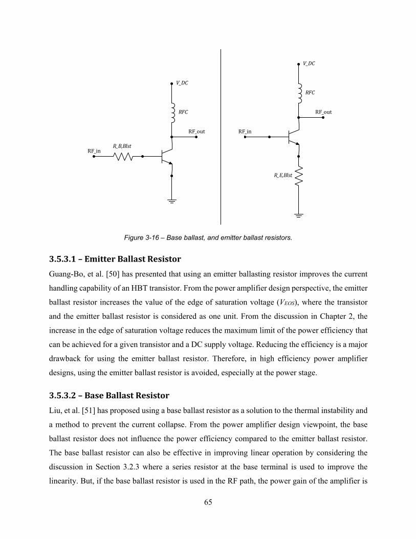
65
R_B,Blst
V_DC
RF_out
RFC
RF_in
R_E,Blst
V_DC
RF_out
RFC
RF_in
Figure 3-16 – Base ballast, and emitter ballast resistors.
3.5.3.1–EmitterBallastResistor
Guang-Bo, et al. [50] has presented that using an emitter ballasting resistor improves the current
handling capability of an HBT transistor. From the power amplifier design perspective, the emitter
ballast resistor increases the value of the edge of saturation voltage (VEOS), where the transistor
and the emitter ballast resistor is considered as one unit. From the discussion in Chapter 2, the
increase in the edge of saturation voltage reduces the maximum limit of the power efficiency that
can be achieved for a given transistor and a DC supply voltage. Reducing the efficiency is a major
drawback for using the emitter ballast resistor. Therefore, in high efficiency power amplifier
designs, using the emitter ballast resistor is avoided, especially at the power stage.
3.5.3.2–BaseBallastResistor
Liu, et al. [51] has proposed using a base ballast resistor as a solution to the thermal instability and
a method to prevent the current collapse. From the power amplifier design viewpoint, the base
ballast resistor does not influence the power efficiency compared to the emitter ballast resistor.
The base ballast resistor can also be effective in improving linear operation by considering the
discussion in Section 3.2.3 where a series resistor at the base terminal is used to improve the
linearity. But, if the base ballast resistor is used in the RF path, the power gain of the amplifier is

66
reduced and may cause a degradation in the power-added efficiency. Therefore, it is recommended
to use the smallest resistor value that is sufficient to improve the thermal stability.
A simple approach to retrieve some of the reduced power gain due to the base ballast resistor
in the RF Path, when used to improve the thermal stability, is to bypass the resistor by a capacitor,
as shown in Figure 3-17. Such a configuration allows the ballast resistor to be effective in
balancing the DC current among the parallel cells, while the bypass capacitor provides a lower
impedance at the fundamental frequency to achieve a minimum decrease of the power gain.
R_B,Blst
V_DC
RF_out
RFC
RF_in
C_B,Blst
Figure 3-17 – A bypassed base ballast resistor.
To further illustrate the effect of such a configuration and help selecting the proper value of
the bypass capacitor, the following analysis derives the transfer function of the base ballast resistor
(RB,Blst) and the bypass capacitor (CB,Blst) when terminated by a resistor (Rin,Dev) that represents the
input impedance of a transistor (to simplify the analysis), as shown in Figure 3-18.
R_B,Blstv_in
C_B,Blst R_in,Dev
v_out
Figure 3-18 – A bypassed base ballast resistor loaded by the input impedance of a transistor.

67
The impedance of the ballast resistor and the bypass capacitor is given by
,1
1
,,
,
1 , ,
( 3-14 )
The transfer function of the circuit shown in Figure 3-18 is calculated as
,
, ,
,
,
1 , ,,
, 1 , ,
, , 1 , ,
1 , ,
,
,1 , ,
1 , ,
, ,
,, ,
,
, ,
1 , ,
1 , ,
, ,,
,
, ,
1 , ,
1 , || , ,
( 3-15 )
From Equation ( 3-15 ), the transfer function contains a zero (z1) and a pole (p1). The zero is given
by

68
1 ( 3-16 )
And, the pole is given by
1
, || ( 3-17 )
From Equations ( 3-16 ) and ( 3-17 ), and since RB,Blst > (RB,Blst || Rin,Dev) then z1 < p1 , causing the
frequency response to be of a high-pass form. Hence, in order to reduce the effect of the bypassed
ballast resistor at the fundamental frequency (ω0), the design target is to decrease the pole (p1) by
increasing the capacitor value (CB,Blst), such that p1 < ω0 .
3.6–Summary
This chapter presented a detailed discussion about the linearity in power amplifiers. Few of the
highlighted issues are: the nature of nonlinearity is categorized as weak and strong nonlinearities;
both the amplitude (AM-AM) and phase (AM-PM) distortions causes a waveform distortion; the
operation with a reduced conduction angle exhibits a form of nonlinearity. The transistor
characteristics affect the linearity, such as the expansive transconductance of the HBT can be
utilized to reduce the nonlinearity inherited from the operation with a reduced conduction angle.
Also, the elimination of the odd-degree harmonic components at the output of the transistor may
improve linearity.
Investigations of techniques to linearize the relationship between the collector current and the
input voltage of an HBT-based power amplifiers were presented, such as using a series resistor
with the base terminal, while considering the effects of both the bias circuit output impedance and
the input matching network frequency response. Multiple bias circuits were discussed aiming at
obtaining a bias circuit that provides temperature compensation and reduces the bias depression
phenomenon that occurs in HBT power transistors at high output power levels.

69
4.
ADesignMethodologyforBroadbandMatching
Networks
4.1–Introduction
Matching networks play a dominant role in RF and microwave circuits. Almost all elements of a
wireless communication system (low noise amplifier, mixer, voltage controlled oscillator, and
RF/microwave amplifier) contain matching networks. Typically, matching networks are required
to provide impedance transformation as well as course bandwidth control. If critical filtering
characteristics are required, a dedicated filter is used in the RF system.
The output matching network of a power amplifier has more requirements to satisfy compared
to matching networks of other system elements. In power amplifiers, the output matching network
is required to provide an impedance transformation from 50 Ohms (typical) to a specific load at
the fundamental frequency, at the transistor, to obtain a specified output power. For a multi-band
power amplifier, this requirement is extended to have a broadband impedance transformation. In
high-efficiency power amplifiers, the output matching network is required to present specific
harmonic terminations, at the transistor, which are needed to engineer voltage and current
waveforms in order to achieve high power efficiency.
Additionally, the output matching network is also required to establish filtering characteristics
to reject the generated harmonics within the power amplifier. This requirement mandates that the
frequency response be of a low-pass filter form. A ladder network of series inductances and shunt
capacitances is widely used for that purpose. For higher attenuation at out-of-band frequencies, the
series self-inductance of shunt capacitors, in addition to a small printed inductance are used to
create a notch in the frequency response, modifying the response to be of an elliptic filter form.
Design specifications for matching networks focus on the impedance transformation, out-of-
band attenuation, network loss, and network size. The designer may need to make a trade-off
among two or more of the design specifications. Classical design techniques do not provide the
designer with the needed degrees of freedom to achieve such a trade-off.

70
Although, the design of matching networks has been investigated for many decades, the
literature lacks a sufficient discussion of design techniques where lossy components are used. Most
well-known design techniques, such as tables of impedance-transforming networks and Smith
chart design, assume ideal components with no loss. Typical effects of using lossy components in
a matching network that is designed with a no loss assumption are:
The network frequency response is shifted away from the ideal case. The shift is more
severe for a narrow-band frequency response.
The network presents a different transformed impedance.
Power dissipation occurs in the network, degrading the efficiency of the network and
reducing the maximum power delivered to the load.
This chapter presents a new approach to design broadband matching networks where lumped
components with a low quality factor exist. The design technique provides an accurate impedance
transformation at a specified frequency, higher attenuation at out-of-band frequencies and/or
reduction of the number of sections in the network. Also, it offers more degrees of freedom to meet
different design requirements. It provides better characteristics without changing the network
topology, while using the same or fewer components. The technique can be extended to employ
the stagger-tuning to increase the flatness of the in-band frequency response.
The design approach is intended to be a simple and accurate first-hand calculation, at the first
phase of the design, which reduces the simulation and optimization time. Also, it can be
implemented as a computational program. The approach is valid for impedance-transforming
networks that contain more than four components or a cascade of single-section networks. The
technique relies on the design equations of single-section networks (L-network, and T-network).
The approach extends the use of those design equations by including the component loss.
Since the inductor quality factor is much lower than that of a discrete capacitor, the focus is
on the inductor loss rather than both components. All design techniques which are presented in the
chapter are valid to design matching networks for any RF system element.
4.1.1–Background
One technique of designing a matching network is to use tables of impedance-transforming
networks of low-pass filter form. Such tables are presented by Matthaei [12] for a Chebyshev
response and by Cristal [13] for a maximally-flat (Butterworth) response. Zhu and Chen [52]

71
presented formulas as a replacement to the tables. This technique provides a ladder network of
series inductances and shunt capacitances. The attenuation characteristics of these matching
networks are obtained by mapping the attenuation characteristics of typical low-pass filters using
a mapping function. It should be noted that typical low-pass filters have termination resistances of
equal values while matching networks have termination resistances of different values.
Another technique of designing matching networks is based on single-section matching
networks of different topologies (L-network, T-network, and Pi-network). A set of design
equations for each topology is derived by combining the concepts of series/parallel resonance with
series/parallel impedance transformation.13 Almost all design equations available in literature
assume ideal components with no loss. Broadband response can be achieved by cascading multiple
sections. Designing the matching network as a cascade of single-section networks allows applying
a few techniques available in filter theory to improve the network characteristics. For example, the
technique of stagger-tuning can be utilized to increase the flatness of the in-band frequency
response, Sedra and Smith [53].
The Smith chart has been used as a handy tool for designing lumped and distributed matching
networks. Both narrow-band and broadband matching networks can be designed using the Smith
chart following the typical topologies (L-network, T-network, and Pi-network), as presented by
Gonzalez [14]. In power amplifiers, the Smith chart provides an insight of the load that is presented
to the transistor since load-pull contours are usually plotted on the Smith chart.
Techniques of designing broadband matching networks using transformers have been
available for decades, as presented by Clarke and Hess [15] and Krauss, et al. [25]. Although,
using transformers for broadband matching networks provides better results compared to other
techniques, it has a restricted application in industry due to limitations that require designing for
small die and module size. Recently, investigations to implement on-chip transformers as part of
output matching networks were carried out, Hoseok, et al. [16] and Hua, et al. [54].
Power efficiency is a major design goal in power amplifiers. Understanding the matching
network efficiency is important to improve the overall efficiency of the power amplifier. The
problem of transferring maximum power to a resistive load by a matching network that contains
lossy components was discussed by Gilbert [55]. Interesting considerations for the design of high-
efficiency matching networks were presented by Yehui and Perreault [56]. It was shown that the
13 ‐ This technique is discussed in details in section 4.2.

72
network efficiency is a function of the inductor quality factor (qL) and the transformation variable
(q) that is introduced in the design. Increasing q decreases efficiency, while decreasing qL
decreases efficiency. Assuming a matching network of cascaded L-network sections, there is an
optimum number of sections to achieve maximum efficiency. Those considerations may lead to
the possibility of achieving higher efficiency by decreasing the number of sections while
increasing qL of the inductor of each section.
4.2–Single‐SectionNetworks
The design equations of a single-section matching network (L-network, T-network, and Pi-
network, shown in Figure 4-1) are available in literature, assuming ideal components with no loss.
Davis [57] has presented one method of deriving those equations by combining the two concepts
of series/parallel resonance with series/parallel impedance transformation.
X_Ss X_Ls
X_Mp
X_Ms
X_LpX_Sp
X_Ss
X_Lp
X_Ls
X_Sp
Pi‐networkT‐network
L‐network
Figure 4-1 – The L-network, T-network, and Pi-network.14
Series/parallel resonance occurs in a resonant circuit when the reactive part vanishes leaving
a real resistive part, at a single frequency or a multiple of frequencies. Such a circuit must include
opposite types of reactive components, inductance and capacitance. In a resonant circuit with a
single resonant frequency, the bandwidth is directly related to the circuit quality factor (Q). The
14 - Subscripts: “L” refers to the load terminal, “S” refers to the source terminal, “M” refers to the middle component, “s” refers to a component in series, and “p” refers to a component in parallel.
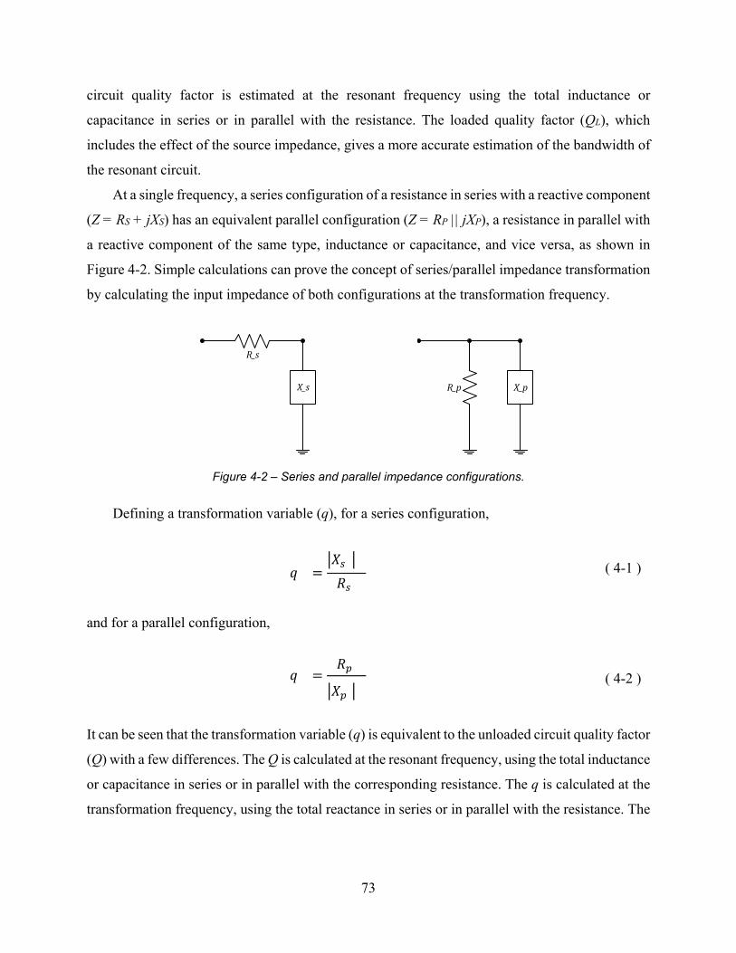
73
circuit quality factor is estimated at the resonant frequency using the total inductance or
capacitance in series or in parallel with the resistance. The loaded quality factor (QL), which
includes the effect of the source impedance, gives a more accurate estimation of the bandwidth of
the resonant circuit.
At a single frequency, a series configuration of a resistance in series with a reactive component
(Z = RS + jXS) has an equivalent parallel configuration (Z = RP || jXP), a resistance in parallel with
a reactive component of the same type, inductance or capacitance, and vice versa, as shown in
Figure 4-2. Simple calculations can prove the concept of series/parallel impedance transformation
by calculating the input impedance of both configurations at the transformation frequency.
R_s
X_s X_pR_p
Figure 4-2 – Series and parallel impedance configurations.
Defining a transformation variable (q), for a series configuration,
( 4-1 )
and for a parallel configuration,
( 4-2 )
It can be seen that the transformation variable (q) is equivalent to the unloaded circuit quality factor
(Q) with a few differences. The Q is calculated at the resonant frequency, using the total inductance
or capacitance in series or in parallel with the corresponding resistance. The q is calculated at the
transformation frequency, using the total reactance in series or in parallel with the resistance. The

74
loaded quality factor (QL) includes the effect of the source impedance while q does not include the
source impedance effect.
Since both series and parallel configurations must be equivalent at the transformation
frequency then
( 4-3 )
Writing the impedance of a parallel configuration in the form of (Z = RS + jXS), leads to
1 ( 4-4 )
1 ( 4-5 )
It should be noted that in all cases
( 4-6 )
( 4-7 )
Also, the transformation from series to parallel equivalent, and vice versa, does not alter the sign
of the reactive component. Therefore, a series inductance transforms to a parallel inductance.
There are multiple realizations for each single-section network (L-network, T-network, and
Pi-network) by selecting each reactive component to be an inductance or a capacitance. The
suitable realization is selected based on whether the network is needed to have a low-pass, high-
pass or band-pass frequency response, and up-transformation or down-transformation. Another
limitation is based on which realization gives realizable component values. Additional constraints,
to limit the bandwidth or to include notches in the frequency response, may replace one element
with a parallel or series reactive circuit that includes additional elements.
4.2.1–TheL‐Network
The design equations of a basic L-network can be derived by combining the concepts of impedance
transformation and resonance. Assuming a down-transformation of resistance, that transform from
RL to RT such that RL > RT. Adding a reactive component XLp in parallel with RL, creating (XLp ||

75
RL), causes the equivalent series configuration to have a smaller resistance. Adding XSs, of opposite
type than XLp, in series with (XLp || RL) to resonate out the series reactance of the equivalent series
configuration leaves only the smaller resistance at the resonant frequency, shown in Figure 4-3. A
similar method can be applied to achieve an up-transformation of resistance by reversing the L-
network.
The concept of resistance transformation can be extended to a complex impedance
transformation. First, achieving a resistance transformation then modifying the reactive
components at the terminals of the network to transform from one complex impedance to another.
R_LX_Lp
X_Ss
R_T
Figure 4-3 – The down-transformation L-network.
4.2.1.1–TheDesignEquationsoftheL‐Network
The basic design equations can be summarized as
1 ( 4-8 )
( 4-9 )
( 4-10 )
( 4-11 )
where XLp and XSs are calculated at f0 which is the transformation frequency and the resonant
frequency at the same time. Assuming conjugate match source impedance, we find QL = Q / 2.
It should be noted that using the design equations gives an exact resistance transformation at
the transformation frequency and a reasonable response around the design frequency. The loaded
quality factor (QL) can be used to estimate the bandwidth which is valid in a small vicinity around

76
the transformation frequency that is assumed to be the center frequency of that bandwidth. The
calculated bandwidth is an approximation due to the assumption of having an equivalent series
resonant circuit, created by XSs and the equivalent series of XLp. That can be clarified by comparing
the frequency response of a resonant circuit (series or parallel) which is of a band-pass form, with
the response of an L-network which is of a low-pass or high-pass form.
The L-network has only two degrees of freedom. Determining the impedance transformation
and the transformation frequency, forces the bandwidth and Q to a specific value. Another degree
of freedom is needed in order to control the bandwidth. Adding another reactive component to the
L-network gives another degree of freedom as implemented in the T-network, and Pi-network.
4.2.2–TheT‐Network15
Multiple realizations of the T-network can be implemented by selecting each reactive component
to be an inductance or capacitance. The analysis in this section is presented for the realization
where the shunt component is an opposite type relative to the two series components. For example,
the LCL T-network which has a low-pass frequency response that is needed for the output
matching network of a power amplifier, shown in Figure 4-4.
X_Mp
X_Ss
R_TR_L
X_Ls
Figure 4-4 – The LCL T-network.
Same techniques of impedance transformation and resonance can be applied to derive the
design equations of the T-network. The derivation starts by transforming the series to parallel
configuration, then transforming the resultant parallel combination from parallel to series again.
The isolated reactive component, which is the single inductance or capacitance in the network,
determines the approximate bandwidth and the circuit quality factor (Q). By including the effect
of the source impedance (ZS), the Q can be derived by calculating the total resistance in parallel
15 - The design equations of the Pi-network are presented in appendix A4.3.

77
with XMp, which is the equivalent parallel of RL in parallel with the equivalent parallel of RS. The
isolated reactive component is calculated as the reactive component that is needed to resonate-out
the equivalent parallel configurations of both XSs and XLs.
4.2.2.1–TheDesignEquationsoftheLCLT‐Network16
The main design equations for the T-network are summarized as
1 1 ( 4-12 )
( 4-13 )
( 4-14 )
1
1 ( 4-15 )
1 ( 4-16 )
The last equation is only valid for the realization where XMp is the isolated reactive component, in
the case of the LCL T-network. If Q includes the effect of the source resistance, then it represents
the loaded quality factor (QL).
It should be noted that the T-network is more suitable to small termination resistances due to
the internal up-transformation that occurs within the network. Using the design equations of the
T-network determines three characteristics: impedance transformation, transformation frequency,
and bandwidth. Compared to the equations of the L-network, the equations of the T-network
liberate the impedance transformation ratio from Q. As a result, the design equations of the T-
network provide more degrees of freedom to implement the design.
4.3–BroadbandNetworks
The output matching network of a handset power amplifier is required to transform the impedance
from 50 Ohms to few Ohms. A single-section matching network may provide the needed
16 - Derivation of the design equations of the T-network, in the general case, is presented in appendix A4.2.

78
transformation with a narrow-band frequency response, but inadequate filtering at the harmonic
frequencies. In order to obtain a broadband response and increase the attenuation at out-of-band
frequencies, multiple single-section networks are cascaded. To reject the generated harmonics, the
network response is required to be of a low-pass form. Therefore, the matching network topology
takes the form of a ladder network of series inductances and shunt capacitances, as shown in Figure
4-5. One difference, compared to the typical ladder network, is the additional up-transformation
L-network section (S4). It is used in power amplifiers to provide a specific harmonic termination
which depends on the operating class of the power amplifier (class-AB, -E, -F, -J …). Additional
rejection to the generated harmonics can be achieved by employing the self-inductance of shunt
capacitors while adding a small inductance in series, creating a series resonance and transferring
the response to be of an elliptic filter form.
Z_T4R_L
DCB
Z_T3 Z_T2 Z_T1
S1S2S3S4
Figure 4-5 – A typical output matching network of a power amplifier.
One typical design approach is to think in terms of a cascade of single-section L-networks.
The network can be divided into three down-transformation L-networks (S1, S2 and S3) followed
by one up-transformation L-network (S4). The shunt capacitor of the last section (S4) is usually
implemented on the die, as close as possible to the collector of the power transistor. The shunt
capacitor value is critical to the power amplifier performance in terms of power efficiency and
linearity. Since it is implemented on the die, the capacitor value has a maximum size limitation.
The series inductance of S4 is due to the bond-wire, or bump pillar in a flip-chip process, that is in
series with a printed inductance on the laminate. Given the required value of the transformed
impedance (ZT), the shunt capacitor value of S4, and the inductance of the bond-wire or bump
pillar, ZT3 can be determined. Once RT3 is determined, it is a direct process to use the design

79
equations of the L-network, or use the Smith chart, to design each section of the three down-
transformation sections (S1, S2 and S3). By choosing suitable impedance transformation ratios,
and limiting each transformation variable (q) to be below 2.5, reasonable wideband performance
can be achieved, and realizable component values can be obtained.
4.3.1–ChallengesoftheTypicalDesignApproach
The design equations of the L-network depend only on the resistance transformation ratio at the
transformation frequency. They do not provide any bandwidth control. Hence, the rejection of out-
of-band frequencies is not controlled.
The equations assume ideal reactive components with no loss. Using lossy components to
implement a network that is designed with a no-loss assumption causes a change in the transformed
impedance, a shift in the frequency response, and a power dissipation in the network, reducing the
power efficiency of the network and the overall power amplifier efficiency.
Typically, each section is designed at the same transformation frequency. Minimum insertion
loss of each section occurs at the transformation frequency. By cascading multiple sections with
high Q, the difference between the insertion loss at the transformation frequency and the insertion
loss at band-edges is expected to increase. It should be noted that the transformation frequency is
approximated as the center frequency of the frequency band of interest.
Adding a small inductance in series with the shunt capacitor of each section increases the
rejection at harmonics. But, it significantly shifts the frequency response, and alters the
transformed impedance, mandating the application of a compensation technique.
4.3.2–DesignExample
This design example demonstrates the challenges of the typical design approach discussed in last
section. Since the last section (S4) is usually limited by other considerations, such as the maximum
on-chip capacitor value, and the required harmonic terminations based on the operating class of
the power amplifier, the design methodology is focused on designing the off-chip cascade of down-
transformation L-networks (S1, S2, and S3).
The output matching network of a power-amplifier module for a handset may need to provide
an impedance transformation from 50 Ohms to 1.8 Ohms (before S4) within the frequency band
(824 MHz – 915 MHz). Using the design equations at the transformation/center frequency (f0 =
870 MHz) and assuming inductor quality factor qL = 30. In order to obtain realizable component

80
values, it is recommended to design each section such that q1 ≈ 1, q2 ≈ 1 to 1.5 and q3 ≈ 1.5 to 2.5.
Component values obtained assuming no loss in the design equations are shown in Table 4-1.
Figure 4-6 shows the symbolic L-network section that corresponds to the table.
Section (Sn)
Ω
Ω
,
S3 2.13 1.8 10 0.70 39.05 0.21 2 S2 1 10 20 1.83 9.15 0.41 3 S1 1.2 20 50 4.48 4.48 0.30 5
Table 4-1 – The component values of the typical design process without loss.
R_T
L_Lp
C_Lp
L_Ss
R_L
Figure 4-6 – The L-network with series inductor in the shunt branch.
The matching network has been simulated for three different cases:
Case 1 (LLL_3S_Ideal): Simulating the network using ideal components with no inductor
loss and without adding the series inductors (LLpn) in the shunt branches to create the
notches in the frequency response.
Case 2 (LLL_3S_qL): Simulating the network while applying the inductor loss (qL = 30)
but without adding the series inductors in the shunt branches.
Case 3 (LLL_3S_qL_0s): Simulating the network while applying the inductor loss (qL =
30) and adding the series inductors in the shunt branches to achieve higher attenuation at
out-of-band frequencies, but without compensating for it.
Simulation results presented in Figure 4-7 to Figure 4-9 shows the effects that have been
discussed, such as the frequency response shift, and the alteration of the transformed impedance.

81
Figure 4-7 –The attenuation at out-of-band frequencies.
Figure 4-8 – The shift in frequency response and higher insertion loss.
S21
(dB
)S
21 (
dB)

82
Figure 4-9 – The deviation in the real part of the transformed impedance from the targeted value of 1.8
Ohm.
Figure 4-7 shows the increased attenuation at the out-of-band frequencies, in case 3
(LLL_3S_qL_0s), due to the addition of the series inductors in the shunt branches. Figure 4-8
shows the shift of the frequency response. The shift is significant in case 3 (LLL_3S_qL_0s)
compared to the ideal case (LLL_3S_Ideal). Also, Figure 4-8 shows the higher insertion loss of
the network when applying the inductor loss in simulation. Figure 4-9 shows the deviation of the
transformed impedance. The deviation in the transformed impedance is more severe in case 3
(LLL_3S_qL_0s) compared to the ideal case (LLL_3S_Ideal).
4.4–NewDesignMethodology
The proposed process to design a matching network is focused on solving the main issues of the
typical design approach. The process is intended to take place at the first phase of the design cycle.
The last section (S4) is usually limited by other considerations, such as the maximum on-chip
capacitor value, and the required harmonic terminations for the operating class of the power
amplifier. Therefore, the design methodology is focused on designing the off-chip cascade of
down-transformation L-networks (S1, S2 and S3). The off-chip cascade of the network, as shown

83
in Figure 4-5, can be visualized differently, as shown in Figure 4-10. The network is designed as
a cascade of three T-networks (S1, S2 and S3). This approach is intended to maintain the same
topology as in Figure 4-5, by considering every two inductors in series as a single inductor. Also,
it utilizes the DC blocking capacitor to be part of the matching network.
Z_T3R_L
Z_T3 Z_T2 Z_T1
S1S2S3
Figure 4-10 – The proposed technique to design the matching network.
The main specifications for output matching networks of power amplifiers are accurate
impedance transformation, harmonic attenuation, and power loss. For handset power amplifier
modules, a compact size is another requirement. The methodology aims at providing the designer
with more degrees of freedom to meet the design specifications by choosing the appropriate trade-
offs. Hence, the T-network has been adopted in the design process instead of the L-network since
it provides more degrees of freedom. The main drive of the design technique is to obtain an
accurate impedance transformation at the specified transformation frequency, while including the
component loss. The out-of-band attenuation is managed by controlling the quality factor (Q) of
the T-network. The design methodology can be extended to applying the stagger-tuning technique
by designing each section of the network at a different transformation frequency to reduce the
insertion loss variation across the required bandwidth.
4.4.1–FeaturesoftheProposedDesignApproach
4.4.1.1–ControllingtheHarmonicRejection
Using the design equations of the T-network provides a bandwidth control, in addition to the
impedance transformation. Targeting the same impedance transformation, each section can be

84
designed for a higher Q to increase the attenuation at harmonics. A comparison between the
frequency response of one L-network and one T-network is shown in Figure 4-11. Each network
transforms the impedance from RL = 25 Ohms to RT = 10 Ohms at f0 = 870 MHz. The T-network
is designed for QL = 1.5 while the L-network provides a loaded quality factor QL = 1. The result
shows that a small increase in Q may add significant attenuation at the out-of-band frequencies.
Figure 4-11 – Comparison between the L-network and T-network.
In power amplifiers where voltage and current waveforms are engineered for high efficiency,
the last section (S4) may need to block harmonic current components from passing to other
sections and forcing them to flow in the capacitor to wave-shape the current and voltage
waveforms at the collector. Such a requirement enables replacing three off-chip matching sections
with two sections only, since harmonic current components are lower and less attenuation is
needed by the matching network. The design of a two-section network requires designing each
section at a lower Q in order to maintain a broadband response. In power-amplifier modules for
handsets, small inductor values are required for small module size and lower power loss.
Therefore, each section can be designed at a specified Q that achieves the needed inductor value.
It should be noted that such trade-offs are difficult to achieve using the design equations of the L-
network, or other classical techniques such as those mentioned in section 4.1.1, compared to using
1 2 3 4 50 6
-40
-30
-20
-10
-50
0
freq, GHz
S21
(dB
)
L_Net_S21
T_Net_S21

85
the design equations of the T-network which enable designing for the impedance transformation
and a specified Q independently.
4.4.1.2–AccountingfortheComponentLoss
An investigation on using the design equations of the L-network and T-network has been carried
out to realize the capability of extending their use to include the component loss. For a given load
and source impedance and with the knowledge of an approximate value of the component loss, it
has been found that the equations can be used to perform a single task from the following, but not
both at the same time:
The impedance can be accurately transformed at a specified frequency.
The center frequency of the targeted bandwidth can be set to a specified frequency.17
Therefore, the design equations can be used to design the cascade of sections to provide an
accurate impedance transformation at the center frequency of the targeted band while considering
the component loss.
In a power amplifier design, accurate impedance transformation is required at a specified
frequency. In order to design an L-network to transform from RL = 50 Ohms to RT = 25 Ohms,
while compensating for an inductor loss of rL = 1 Ohm, the design equations are used to transform
from RL = 50 Ohms to (RT – rL) = (25 – 1) Ohms. As a result, the total resistance presented to the
source is 25 Ohms.
In other applications, there might be a need to center the frequency response at a specified
frequency for a specified source resistance. Designing an L-network to achieve such a purpose
while providing an approximate impedance transformation from RL = 50 Ohms to RT = 25 Ohms,
the design equations are used at the specified center frequency to transform from RL = 50 Ohms to
(RT + rL) = (25 + 1) Ohms, assuming an inductor loss rL = 1 Ohm.
4.4.1.3–ApplyingtheStagger‐TuningTechnique
Designing each section at a higher Q increases the insertion loss variation across the frequency
band. Applying the stagger-tuning technique, such that each section of the cascade is designed at
a different transformation frequency, reduces the insertion loss variation within the specified band.
Therefore, the stagger-tuning technique can be utilized to compensate for the effects of designing
17 - This task is valid assuming the network is presenting a conjugate match impedance to the source. Refer to appendix A4.1 for details.

86
for a higher Q and positioning the frequency response of the entire network around the center
frequency of the band (f0) by designing one section to transform the impedance at f0, another
section at fL < f0, and the third section at fH > f0.
4.4.1.4–CompensatingfortheEllipticFrequencyResponse
Using the T-network with a higher Q in the design provides more attenuation at out-of-band
frequencies. That attenuation might be large enough that the design does not need extra zeros in
the transfer function created by adding the inductance in series with the shunt capacitance of each
section. This may be valid only for the fourth and higher harmonics. For the second harmonic, a
small value of inductance in series with at least one of the shunt capacitors is still needed to create
a zero in the transfer function. Creating such a resonance, without any compensation technique,
shifts the frequency response, and alters the transformed impedance. But, simple calculations can
provide an easy fix to the problem in the first phase of the design.
Writing the admittance of a shunt branch of series capacitance (C) and inductance (L) as
1
1 1 1 ( 4-17 )
The admittance can be visualized as an effective capacitance (Ceff)
1 ( 4-18 )
1 ( 4-19 )
where ωr is the resonant frequency of the branch.
Typically ωr is chosen to be at the second or higher harmonics, therefore the frequency band
of interest is at (ω < ωr) where Ceff is positive, YLC is capacitive, and Ceff > C. Adding a small
inductance in series with the shunt capacitor has the effect of increasing the effective capacitance
of the branch that is seen at the band of interest. Which causes the shift of the frequency response
and the change of the transformed impedance. The simple compensation technique can be applied

87
to the network to eliminate those effects by using a smaller value of capacitance to maintain the
original characteristics of the matching network. Given the transformation frequency (f) of the
matching network, the needed capacitance value (Ceff) in the network and the available discrete
capacitance value (C), L can be calculated by calculating ωr from equation ( 4-18 ).
Taking advantage of the fact that adding a small inductor in series with a shunt capacitor
increases its effective capacitance, section S3 is the best choice to add the series inductance. This
choice results from the design equations of section S3 are yielding a high capacitor value causing
the design to be sensitive to the capacitor tolerance. Adding the inductance increases the effective
capacitance, which translates to a smaller capacitance value, and a smaller tolerance value.
4.4.2–TheDesignProcessGuidelines
The design technique requires the knowledge of the inductor loss. Therefore, it has to be an
iterative process where the inductor values and their loss are estimated initially. It is assumed that
the shunt capacitor value of section S4 and the series inductance representing the bond-wire or
bump pillar are pre-determined. For a required value of RT4 that represents the transistor load, the
real part of ZT3 (RT3) is determined from S4. The following are the guidelines of the design process:
A. Determine the initial transformed impedances and establish a reference for out-of-band
attenuation:18
Select RT1 and RT2 using the L-network design equations or the Smith chart approach
to estimate the transformation requirements at the center frequency (f0). Limiting the
transformation variables to q1 ≈ 1, q2 ≈ 1 to 1.5 and q3 ≈ 1.5 to 2.5 provides a reasonable
component values. Also, the loaded quality factor (QL = qn / 2) gives an indication of
the out-of-band attenuation and provides a reference if a higher or lower attenuation is
needed.
B. Initial iteration of the solution for the new methodology (TTT network cascade):19
Based on the required specifications, one of the following two approaches can be taken:
Higher out-of-band attenuation than what can be achieved by the L-network
approach: Use a T-network design. Using the T-network equations, design a three-
section network with one or more of the T-network sections to have Qn > qn / 2,
18 - The “qn” refers to the transformation variable of the L-network section. 19 - The “Qn” refers to the loaded quality factor of the T-network section.

88
where Qn is a design variable that is determined by the designer to achieve the
needed attenuation.
Smaller network size or a lower network loss approach: Use the T-network design
equations, design a two-section network with one or more of the T-network sections
to have Qn > qn / 2, after performing step A for a two-section network, to achieve a
broadband frequency response.
Design each section of the network at f0 using the design equations to transform among
RT1, RT2 and RT3 (obtained from the qn) without considering the inductor loss and using
the Qn of the previous step.
From the inductor values, estimate the loss of each inductor and use as initial values in
a second iteration.
C. Second iteration of the solution for the new methodology (TTT network cascade):
For designing a network with low Qn:
Redesign each section to transform among pre-determined impedances from step-
A, while considering the inductor loss in the transformation at f0, as discussed in
section 4.4.1.2.
Add the series resonance of the shunt branches that is needed to reject the
harmonics and compensate for it in the design, as discussed in section 4.4.1.4.
For designing a network with higher Qn, the stagger-tuning technique should be
applied:
Redesign each section to transform among pre-determined impedances, while
considering the inductor loss at a different transformation frequency. The exact
transformed impedance must be calculated for the preceding sections.
Add the series resonance of the shunt branches that is needed to reject the
harmonics and compensate for it in the design, as discussed in section 4.4.1.4.
4.4.3–TheStagger‐TuningConsiderations
Applying the stagger-tuning technique, where each section is designed at a different transformation
frequency, mandates calculating the exact impedance presented by the preceding sections at the
transformation frequency. Analyzing the down-transformation L-network and T-network shows if
one section is designed at a transformation frequency (f0), the reactive part presented by the section
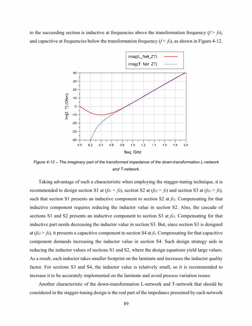
89
to the succeeding section is inductive at frequencies above the transformation frequency (f > f0),
and capacitive at frequencies below the transformation frequency (f < f0), as shown in Figure 4-12.
Figure 4-12 – The imaginary part of the transformed impedance of the down-transformation L-network
and T-network.
Taking advantage of such a characteristic when employing the stagger-tuning technique, it is
recommended to design section S1 at (f01 < f0), section S2 at (f02 = f0) and section S3 at (f03 > f0),
such that section S1 presents an inductive component to section S2 at f02. Compensating for that
inductive component requires reducing the inductor value in section S2. Also, the cascade of
sections S1 and S2 presents an inductive component to section S3 at f03. Compensating for that
inductive part needs decreasing the inductor value in section S3. But, since section S3 is designed
at (f03 > f0), it presents a capacitive component to section S4 at f0. Compensating for that capacitive
component demands increasing the inductor value in section S4. Such design strategy aids in
reducing the inductor values of sections S1 and S2, where the design equations yield large values.
As a result, each inductor takes smaller footprint on the laminate and increases the inductor quality
factor. For sections S3 and S4, the inductor value is relatively small, so it is recommended to
increase it to be accurately implemented on the laminate and avoid process variation issues.
Another characteristic of the down-transformation L-network and T-network that should be
considered in the stagger-tuning design is the real part of the impedance presented by each network

90
decreases as frequency increases, as shown in Figure 4-13. If the network is designed at frequency
f0 to present a real part RT, then it is known that at f > f0, R < RT and at f < f0, R > RT. This fact is
valuable when designing each section at a different frequency and it is required to maintain
realizable values for each section.
Figure 4-13 – The real part of the transformed impedance of the down-transformation L-network and T-
network.
4.4.4–DesignExampleandComparison
The design example in this section is following the design example of section 4.3. It focuses on
designing the off-chip cascade of sections (S1, S2 and S3). Assuming the matching network
cascade is required to provide an impedance transformation from 50 Ohms to 1.8 Ohms (before
S4) in the frequency band (824 MHz – 915 MHz), the design equations are used at the
transformation/center frequency (f0 = 870 MHz), assuming an inductor quality factor qL = 30.
Two different implementations of the new design methodology are compared with the typical
design approach. In all cases, the inductor loss is applied and series inductors are added to the
shunt capacitors of the network to create one or more notches at the out-of-band frequencies. The
stagger-tuning technique is not utilized in the designs, though the simulation results suggest one
might obtain improved in-band flatness for the higher Q example as discussed in section 4.4.1.3.

91
It should be noted that the goal of the comparison is to present the capabilities and show the
available degrees of freedom of the new design methodology compared to the typical design
approach. The three different designs are,
Design “LLL_3S_Typ” represents the typical design approach as mentioned in section 4.3.
The design includes the compensation for adding the series inductors to the shunt
capacitors to achieve an elliptic response. Table 4-2 shows the component values of the
design. Figure 4-14 shows the symbolic L-network section that corresponds to the table.
Design “TTT_3S” represents one implementation of the new design methodology which
aims at achieving a higher out-of-band rejection and a broadband response. The matching
network is designed as a cascade of three T-networks. Table 4-3 shows the component
values of the design. Figure 4-15 shows the symbolic T-network section that corresponds
to the table. The table shows that the design of section S3 targets a higher Q than what
might be needed in a real design. It was elected to take such an approach to demonstrate
the capabilities of the proposed technique.
Design “TT_2S” represents another implementation of the new design methodology which
aims at achieving a smaller size of the matching network and a low power loss while
maintaining a broadband response. The network is designed as a cascade of two T-
networks. Table 4-4 shows the component values of the design. Figure 4-15 shows the
symbolic T-network section that corresponds to the table. The table shows that the design
of each section targets a lower Q than what might be needed. That approach is taken to
demonstrate the capabilities and degrees of freedom of the proposed methodology.
R_T
L_Lp
C_Lp
L_Ss
R_L
Figure 4-14 – The L-network with series inductor in the shunt branch.

92
Section (Sn)
Ω
Ω
,
S3 2.13 1.8 10 0.70 29.29 0.29 2 S2 1 10 20 1.83 8.13 0.46 3 S1 1.2 20 50 4.48 4.3 0.31 5
Table 4-2 – The component values of design LLL_3S_Typ.
R_TC_Mp
R_L
L_LsL_Ss
L_Mp
Figure 4-15 – The LCL T-network with series inductor in the shunt branch.
Section (Sn)
Ω
Ω
,
S3 2.2 1.6 10.36 1 29.71 1.86 - 0.28 2 S2 1.2 9.48 20.56 2.77 11.57 3.01 - 0.32 3 S1 1.2 18.4 50 8.08 1.67 - 3 0.8 5
Table 4-3 – The component values of design TTT_3S.
Section (Sn)
Ω
Ω
,
S2 1.12 1.67 10.02 0.68 30.67 0.01 - 0.27 2 S1 1.2 9.2 50 4.04 5.26 - 7.4 0.4 4
Table 4-4 – The component values of design TT_2S.
It should be noted that an accuracy of two decimal digits is maintained during the design
process. The capacitor values can be adjusted to reflect the discrete component values. In such
case, the values of inductors, which are in series with the shunt capacitors, are required to be

93
adjusted accordingly. But, the printed spiral inductors can be designed and simulated for the same
accuracy using available electromagnetic CAD tools. For high inductor value, a discrete inductor
can be used in series with a printed inductor to achieve the needed value.
4.4.4.1–SimulationResults
The simulation results of the three designs, including one implementation of the typical approach
and the two implementations of the new technique, are presented in Figure 4-16 through Figure
4-19. The goal of comparing the results is to show the effectiveness of the new methodology to
meet different specifications by demonstrating the degrees of freedom and the capabilities that are
incorporated in the methodology. Design specifications of matching networks may include the
impedance transformation, out-of-band attenuation, network loss, and network size.
Figure 4-16 shows the real part of the transformed impedance of each design. The transformed
impedance of the typical design approach (LLL_3S_Typ) is slightly different than the targeted
value, though the effect of the series inductors in the shunt branches have been compensated for
in the design. The deviation of the transformed impedance is expected since the typical design
does not account for the inductor quality factor. Even though the new design methodology was
utilized for two different designs (TTT_3S and TT_2S), the transformed impedance equals the
targeted value in each design.
Figure 4-17 shows S21 for the required frequency band. A shift in the frequency response
occurs when using the typical design technique (LLL_3S_Typ). Both designs which are
implemented using the new methodology (TTT_3S and TT_2S) are centered at the required center
frequency (f0 = 870 MHz). One observation is the insertion loss of design “TTT_3S” is higher than
design “TT_2S” due to the large inductor values which are reflected as a high series resistance.
Although design “TTT_3S” contains three T-network sections, it exhibits a narrower bandwidth
compared to design “TT_2S” which contains two T-network sections. Such observation
demonstrates the capability of the new design methodology, since design “TTT_3S” is targeting a
higher out-of-band attenuation by designing the T-network with a higher Q which is echoed as a
narrower bandwidth. While design “TT_2S” is targeting a smaller network size and a low power
loss while achieving a broadband response by designing the T-network with a lower Q.

94
Figure 4-16 – The real part of the transformed impedance.
Figure 4-17 – The frequency response.
830 840 850 860 870 880 890 900 910820 920
1.6
1.7
1.8
1.9
1.5
2.0
freq, MHz
real(LLL_3S_Typ_ZT)
real(TTT_3S_ZT)
real(TT_2S_ZT)
S21
(dB
)

95
Figure 4-18 shows the rejection of out-of-band frequencies for each design. The typical design
technique (LLL_3S_Typ), where no control of the out-of-band frequencies exist, is considered as
the reference for comparison. Design “TTT_3S” achieves a higher rejection which is targeted by
designing the T-network with a higher Q. Design “TT_2S” achieves a lower rejection which is
targeted by designing the T-network with a lower Q. The results display the potential capability of
the new methodology, where the attenuation of out-of-band frequencies is controlled.
Figure 4-18 – The harmonics attenuation.
Figure 4-19 shows the power loss of each design. The typical design technique (LLL_3S_Typ)
is taken as the reference for comparison. Design “TTT_3S” has a higher loss which is expected
since the T-network sections are designed with a higher Q, which is reflected as a larger inductor
values with a higher loss. Design “TT_2S” has almost the same loss, while using only two sections
instead of three, by designing the T-network with a lower Q, which is echoed as a lower inductor
value and a lower loss. The results show another potential capability of the new methodology
where the network loss and size are controlled.

96
Figure 4-19 – The power loss within the network.
4.4.5–Discussion
4.4.5.1–DifferentApproach
Although the presented design methodology focuses on the output matching network of a power
amplifier, it can be used to design any matching network topology with multiple sections. All other
types of matching network sections (L-network, T-network, and Pi-network) can be employed in
the design methodology, after characterizing each type and understanding how it can be utilized
to help the entire network performance.
The typical network topology, shown in Figure 4-5, can be analyzed as a cascade of CCL T-
network, CLC Pi-network, and another up-transformation L-network, as shown in Figure 4-20. It
was found, that such configuration yields un-realizable values for reactive components. As, the Pi-
network internally transforms the impedance down and then transforms back up. But, since the
load and transformed impedances in a power-amplifier module are in the range of few ohms, the
internal down-transformation would yield impedances in milli-ohms. Another reason to avoid such
a configuration is the difficulty of engaging the reactive part presented by one section into the
succeeding section, when designing each section at a different transformation frequency.
8.3E8 8.4E8 8.5E8 8.6E8 8.7E8 8.8E8 8.9E8 9.0E8 9.1E88.2E8 9.2E8
0.6
0.8
1.0
1.2
1.4
1.6
0.4
1.8
freq
LLL_3S_Typ_PLoss
TTT_3S_PLoss
TT_2S_PLoss

97
Z_T3R_L
DCB
Z_T3 Z_T2 Z_T1
S1S2S3
Figure 4-20 – A different configuration to analyze the matching network.
4.4.5.2–Stagger‐tuningGeneralization
Applying the stagger-tuning technique can be generalized to be used among different matching
networks in the design. In a power amplifier of two stages of amplification, the input matching
network can be designed for a transformation frequency, the inter-stage matching network can be
designed for a second frequency, then the output matching network can be designed for a third
frequency. Such an approach is expected to increase the flatness across the overall in-band
frequency response of the entire amplifier.
4.5–Summary
This chapter presents a new design methodology for broadband matching networks. The new
design technique aims at providing the designer with more degrees of freedom to meet the design
specifications of broadband matching networks, such as the impedance transformation, out-of-
band attenuation, network loss, and network size. However, the classical design techniques, such
as the tables of impedance-transforming networks, the Smith chart design, and a cascade of L-
networks, do not provide the designer with the needed degrees of freedom.
The new design approach provides an accurate impedance transformation at a specified
frequency, and the capability of controlling the attenuation at out-of-band frequencies and/or
reducing of the number of sections in the network. While the technique relies on the design
equations of single-section networks (L-network, and T-network), it extends the use of those
design equations by including the component loss. The technique can be expanded to employ the
stagger-tuning to increase the in-band flatness of the frequency response and increase the

98
bandwidth, though this step was not pursued. The methodology also provides a simple method to
compensate for adding series inductors in the shunt branches to provide harmonic notches in the
frequency response and transforming it to an elliptic response.
The new methodology focuses on designing the typical ladder network of series inductors and
shunt capacitors as a cascade of T-networks, rather than a cascade of L-networks, to take advantage
of the more degrees of freedom offered by the design equations of the T-network. Therefore, the
new methodology provides better characteristics without changing the basic network topology,
while using the same or fewer components. The new approach is valid for impedance-transforming
networks that contain more than four components or a cascade of single-section networks. The
design approach is intended to be a simple and accurate first-hand calculation at the first phase of
the design, reducing the simulation and optimization time.

99
Appendix
A4.1–Assumptions
A4.1.1–ConjugateMatch
Typically, in power amplifiers, the output impedance of the transistor is different than the
conjugate of the impedance presented by the matching network. The analysis presented in this
chapter assumes that the design of the matching network is targeting a conjugate match. This
assumption has been adopted to simplify the design equations. Specially, it has a minimal effect
on the final results of the design. That is due to the fact that the presented technique starts by
designing a network of low-pass filter form with low quality factor and wide bandwidth, then
adjust it to be of an elliptic filter form. Therefore, the bandwidth is narrower and is determined by
the zeros of the transfer function of the network. Hence, the analysis is valid in both cases of
designing for conjugate match or the output matching network of a power amplifier. It should be
noted that varying the quality factor (Q) of each section is intended to control the rejection of the
out-of-band frequencies rather than to control the bandwidth.
A4.1.2–CascadeofSections
The design of the entire matching network is considered as a cascade of matching sections. Each
section is designed separately. Such approach enables simplifying the design process and adds
more degrees of freedom, for example, designing each section at a different center frequency,
while maintaining the integrity of the design. The main characteristic that is used to evaluate the
frequency response of each section is |S21|. For a conjugate match design, |S21|2 = GT, where GT is
the transducer power gain, Gonzalez [14]. For a cascade of networks GTNet = GT1 GT2 GT3, which
justifies the idea of designing the entire network as a cascade of sections.
A4.1.3–ApproximateModel
The adopted design equations are based on the equivalent circuit model of the exact circuit around
the transformation frequency. This approximation is valid as long as the analysis is restricted to
the vicinity around the transformation frequency. In case of applying the stagger-tuning technique,
where each section is designed at a different transformation frequency, an exact analysis is required
to calculate the impedance presented by the preceding cascade of sections.

100
A4.2–DerivationoftheT‐NetworkDesignEquations
This section presents the derivation of the T-network design equations, in details, following the
derivation presented by Davis [57].
There are six possible realizations of the T-network, shown in Figure 4-21. If the isolated
component is XLs or XSs, the smaller termination resistance must be in series with the isolated
component. Assuming a lossless network, this limitation is due to the fact that the other two
components creates a voltage divider, while the power is the same at every node in the network.
X_Ss X_Ls
X_MpZ_T
R_L
Figure 4-21 – The T-network.
The shunt reactive component can be calculated as the reactive component needed to resonate-
out the equivalent parallel of both XSs and XLs,
1 1 1 ( 4-20 )
where, XSsp is the equivalent parallel of XSs and XLsp is the equivalent parallel of XLs.

101
1 1 1
11
11
11
11
∓ 1 ∓ 1
( 4-21 )
where
( 4-22 )
( 4-23 )
Using
1 1 ( 4-24 )
Then,
1 ∓ ∓
1 ( 4-25 )
It should be noted that the equation carries the sign of the reactive components. If XSs is inductive,
the negative sign of qT is used. If XLs is inductive, the negative sign of qL is used. But, the positive
sign for of qT and qL is used, if XSs and XLs is capacitive.
In case of a general series/parallel impedance transformation with a high transformation
variable (q)

102
( 4-26 )
( 4-27 )
For the T-network,
11
( 4-28 )
Using the high q approximation, equation ( 4-27 ),
( 4-29 )
where, RTp is the equivalent parallel of RT,
1 ∗ ( 4-30 )
( 4-31 )
Same technique can be used to calculate the transformed resistance of RS (RSt) seen looking
into the load port. Assuming a conjugate match at the source RS = RT,20
11
( 4-32 )
1 ( 4-33 )
where, RSp is the equivalent parallel of RS,
1 ( 4-34 )
20 - Refer to appendix A4.1 for discussion about the utilized assumptions.

103
( 4-35 )
A simple method to estimate the bandwidth of the T-network depends on the isolated reactive
component. The loaded quality factor of the circuit is used for accurate estimation of the
bandwidth, therefore the effect of the source resistance is included in the derivations.
There are three cases:
Case 1: the isolated component is XSs,
1 ( 4-36 )
Case 2: the isolated component is XLs,
1 ( 4-37 )
Assuming a conjugate match at the source, RS = RT,
11
( 4-38 )
1 ( 4-39 )
1 ∗ ( 4-40 )
( 4-41 )
Case 3: the isolated component is XMp,
104
||
1 ( 4-42 )
where, RLsp is the equivalent parallel of RLs. Using
1 ( 4-43 )
( 4-44 )
1 ( 4-45 )
A4.3–TheDesignEquationsofthePi‐Network
This section presents the design equations of the Pi-network, as presented by [Davis [57]].
Figure 4-22 shows the Pi-network topology. Applying same techniques as in the T-network,
the following design equations can be obtained.
X_Ms
X_LpX_SpZ_T
R_L
Figure 4-22 – The Pi-Network.
1 1 ( 4-46 )
( 4-47 )
( 4-48 )

105
∓ ∓1
( 4-49 )
A simple method to estimate the bandwidth of the Pi-network depends on the isolated reactive
component. The loaded quality factor of the circuit is used for accurate estimation of the
bandwidth, therefore the effect of the source resistance is included in the derivations.
There are three cases:
Case 1: the isolated component is XSp,
1 ( 4-50 )
Case 2: the isolated component is XLp,
1 ( 4-51 )
Case 3: the isolated component is XMs,
1 ( 4-52 )
It should be noted that, the Pi-network is more suitable to large termination resistance due to
the internal down-transformation that occurs within the network.

106
(This page left intentionally blank)
107
5.
TheDesignofaLinearPowerAmplifierwithHigh
Efficiency
5.1–Introduction
The fast growing market of cellular handsets, with a high demand for better performance and
higher data rates, has led to the coexistence of multiple standards (2G/2.5G/3G/4G). Each standard
utilizes a different modulation scheme with different linearity requirements. For example, the 2G
standard uses Gaussian Minimum Shift Keying (GMSK) modulation that generates a constant
envelope signal, not requiring a linear amplitude amplification. The 4G standard utilizes
Quadrature Amplitude Modulation (QAM) which mandates a high degree of linear amplification.
As a result, handset manufacturers are targeting the design of a single handset that covers the latest
standards (3G/4G) with a backward compatibility to the earlier standards (2G/2.5G).
Different power amplifier module architectures have been proposed to achieve such a
coverage of multiple standards, Cheng and Young [1]. One module architecture, known as a
“hybrid power amplifier”, is to design a single module that contains multiple power amplifiers.
The architecture includes two power amplifiers for the 2G/2.5G modes21 where one covers the low
band and the other covers the mid band. At least, three more linear power amplifiers are needed
for the 3G/4G modes, where each amplifier covers a part or the full bandwidth of one of the major
bands. Another architecture, known as a “converged power amplifier”, is a single module that
contains multiple power amplifiers where each power amplifier covers one of the major frequency
bands while operating in different modes (2G/2.5G/3G/4G). Such an architecture eliminates at
least two power amplifiers with the associate matching networks, typically the power amplifiers
that operate in the 2G/2.5G modes are those to be eliminated.
The optimum design of a converged power amplifier architecture is required to exhibit three
characteristics: high linearity, high efficiency, and broadband frequency response. Chapter 2
through Chapter 4 have presented analysis and discussions about multiple techniques to obtain
21 - The terms “standard” and “mode” are used throughout the dissertation referring to the cellular standard 2G/GSM, 2.5G/EDGE, 3G/W-CDMA, and 4G/LTE.

108
each of these characteristics separately. The investigations presented throughout those chapters
showed that applying one technique to improve one of the characteristics may not satisfy the
others. For example, one technique to obtain high power efficiency is class-E, where the transistor
operates as a switch. A switching operation provides no linear relationship between the amplitudes
of the input and output signals.
A linear power amplifier with high efficiency represents a solution to the “converged power
amplifier” architecture. The required output power of the 2G/GSM mode, is higher than the
required output power of the 2.5G/EDGE, 3G/W-CDMA, and 4G/LTE modes where linearity is
required, as shown in Table 5-1. The distribution of the needed output power levels for these modes
is suitable to be covered by a single power amplifier, since the power amplifier would operate at
the saturated output power in the 2G mode and operates at back-off power levels in the
2.5G/3G/4G modes.
Mode 2G/ GSM
2.5G/ EDGE
3G/ W-CDMA
4G/ LTE
DC Supply Voltage 3.5 V
Frequency Band 814 MHz – 915 MHz (Bands: 5, 6, 8, 18, 19, 20, 26)
Maximum Input Power ( , ) 10 dBm
Maximum Output Power ( , ) 34 dBm 29 dBm 30 dBm 30 dBm
Power Added Efficiency (PAE), at , 55 % 25 % 35 % 35 %
EVM %, at and below , - 3 % 3 % 3 %
ACPR1, at and below , - -33 dBc -33 dBc -33 dBc
Table 5-1 – The design targeted specifications.22
This chapter presents the proposed design techniques to implement a linear power amplifier
with high efficiency and broadband frequency response for handsets, utilizing GaAs HBT process
22 - Due to limitations in the available laboratory tests, the author could not test the 4G/LTE mode.

109
technology. To demonstrate the effectiveness of the proposed design process, a power amplifier
module is designed and implemented. The power amplifier design aims at operating in the
2G/GSM mode with high power efficiency, while meeting the needed linearity of the 2.5G/EDGE,
3G/W-CDMA and 4G/LTE modes. The design targeted specifications are given in Table 5-1.
5.2–TheDesignStrategy
The design strategy of a single-stage linear power amplifier with high efficiency, utilizing a GaAs
HBT process, is to divide the design into two sections, as shown in Figure 5-1.
R_B,Bs
RF_in
V_Reg
BiasCircuit
OutputMatchingNetwork
InputMatchingNetwork
R_L
OutputSectionInputSection
V_DC
RFC
Figure 5-1 – The output and input sections of a single-stage power amplifier.
The first section is the output section of the power amplifier which contains the output current
source of the power transistor and the output matching network. The second section is the input
section of the amplifier which contains the input impedance of the power transistor, the bias circuit,
and the input matching network. It is important to note that the typical design process starts by
designing the output section, followed by the input section. The process is logical since the
transistor is not a unilateral device, causing the input impedance of the transistor to be a function
of the load impedance presented by the output matching network.

110
At the output section, both the high efficiency and broadband frequency response are pursued.
The analysis in Chapter 2 revealed that obtaining a high power efficiency is dominated by the load
impedance presented to the power transistor. Since the unity-gain frequency (fT) of the device is
typically much higher than the third harmonic frequency of operation, the high end of the
frequency response of the power amplifier is dominated by the frequency response of the output
matching network. The design methodology presented in Chapter 4 represents a technique to
obtain the needed broadband matching network. It should be noted that the low end of the
frequency response is determined by the DC blocks, and the input and inter-stage matching
networks topology.
At the input section, the high linearity is pursued. The analysis in Chapter 3 highlighted that
most of the design parameters affecting linear operation exist in the input section of the power
amplifier, such as the series resistor with the base terminal, the input matching network, the
linearization effect of the bias circuit, and the bias circuit output impedance. It is important to note
that those parameters are effective in improving the linear operation, given that the load impedance
presented to the power transistor maintains linear operation.
5.2.1–HighEfficiencyApproach
In wireless handsets, typical design techniques to obtain high efficiency of linear power amplifiers
are deep class-AB, and class-F, Daehyun, et al. [6]. As discussed in Section 2.2.2, the proper
operation of deep class-AB requires the output matching network to present a resistive load at the
fundamental frequency and short-circuit terminations to all harmonics. Class-F operation requires
a resistive load at the fundamental frequency, open-circuit termination at the third harmonic and
short-circuit terminations at all other harmonics, when only the third harmonic is utilized.
The investigation in Section 2.2.4 showed that the second harmonic current component needs
a termination that approximates an ideal short circuit for proper operation, otherwise degradation
in output power and efficiency would occur. In a real design of deep class-AB or class-F, the short-
circuit termination of the second harmonic is implemented by creating a second-harmonic trap at
the collector terminal, Oka, et al. [58]. Typically, the harmonic trap is implemented as a shunt
branch of a series capacitor (on the die) and a small inductor (on the laminate) that resonates at the
second harmonic frequency. The rest of the matching network provides a low impedance at the
other harmonics. In broadband designs, two second-harmonic traps are required. Occasionally, due

111
to a limitation of the die size, the designer of a deep class-AB handset power amplifier may elect
to implement the short-circuit terminations of the harmonics as a single large shunt capacitor rather
than utilizing a separate second-harmonic trap to avoid the space of a bond-pad or bump pillar.
Based on the frequency of operation, the maximum capacitor value used on the die, and the
bandwidth of the notch created by the second-harmonic trap, the harmonic terminations deviate
from the targeted short-circuit termination, causing the power amplifier performance to degrade in
terms of output power, power efficiency and linearity, as presented in Section 2.2.4. Such a
situation often occurs when the harmonic termination is implemented as a single capacitor rather
than a harmonic trap or when utilizing a single second-harmonic trap in a broadband design.
Therefore, the maximum efficiency of deep class-AB (ideal class-B) is not achieved. In addition,
each second-harmonic trap requires a separate bond pad in bond-wire technology or bump pillar
in flip-chip technology. Such a requirement restricts the desired small die size.
As a conclusion, the major problem that hinders the typical techniques (deep class-AB) from
achieving the maximum efficiency lies in the practical implementation of the harmonic
terminations. In order to overcome such problems, the practical implementation of the utilized
technique to obtain high efficiency should avoid the need for a second-harmonic trap and/or
approximated short-circuit terminations at the second harmonic, as much as possible.
5.2.2–LinearityApproach
The investigation in Chapter 2 highlighted that both the selected technique of improving the power
efficiency and the corresponding load impedance affect the linearity. For a given technique of
improving the efficiency, increasing the load above the optimum load causes the collector voltage
waveform to swing into the saturation region of the transistor, creating a high level of harmonic
components that mix within the transistor which degrades both the output power and linearity.
Additionally, Chapter 3 presented the sources of nonlinearity and multiple techniques to
improve the linearity. The analysis showed that the reduced conduction angle technique exhibits a
nonlinearity due to the truncated sinusoid of the collector current which is directly related to the
quiescent bias point. Since HBT transistors show an expansive transconductance, using an HBT
transistor as the power transistor may reduce the nonlinearity of the reduced conduction angle.
The analysis in Chapter 3 showed that few considerations related to HBT transistors are
critical to maintain and improve the linearity. HBT transistors show a nonlinear relationship

112
between the base current and the input voltage of the amplifier due to the nonlinear input
impedance of the transistor causing a nonlinear relationship between the collector current and the
input voltage. But, a linear relationship is required between the collector current and the input
voltage of the power amplifier. One technique to linearize that relationship is to use a resistor in
series with the base terminal. The discussion of Section 3.2.3 showed that the effectiveness of such
a technique does not rely only on the series resistor but also the bias circuit output impedance as
well as the input matching network frequency response.
Also, at high levels of the input drive signal, HBT transistors suffer from a bias depression
phenomenon which is another source of linearity degradation. Section 3.5.2 showed that utilizing
a bias circuit with a linearization effect that reduces the bias depression improves the linearity.
In Chapter 3, it was presented that one important source of waveform distortion is the phase
distortion (AM-PM). In order to obtain a high level of linearity, both AM-AM and AM-PM should
be considered in the design process. It was found that limiting the large-signal power gain variation
(AM-AM) to be less that 0.5 dB and limiting the phase difference variation between the output and
input signals (AM-PM) to be less than 10 degrees within the varying output power region results
in linear operation that satisfies both EVM and ACPR test specifications.
As a conclusion, for a given technique to improve the power efficiency, the load impedance
should be selected to avoid operating into the nonlinear saturation region of the transistor with a
careful choice of the bias point. Utilizing a GaAs HBT power transistor enables multiple tuning
knobs to further improve linear operation.
5.2.3–Class‐JforHighEfficiencyandLinearity
The analysis of class-J in Section 2.3.2 presented that the same maximum efficiency of ideal class-
B is obtained without the need for a perfect short-circuit termination at the second harmonic.
Therefore, class-J may achieve higher practical efficiency than deep class-AB. Also, the analysis
showed that the concept of class-J relies on increasing the minima of the collector voltage
waveform away from the edge of saturation voltage (VCE,EOS). Hence, class-J is suitable for linear
operation since it avoids operating the transistor in the highly nonlinear saturation region.
The analysis of class-J assumed the transistor operates with a linear transconductance between
the collector/drain current and the input voltage of the transistor. That assumption is reasonable
for a field effect transistor (FET), but is not valid between the collector current and the base-emitter

113
voltage of a hetero-junction bipolar transistor (HBT). As a result, class-J has been implemented by
others as a linear power amplifier using only a field effect transistor (FET), while no
implementation has been reported using hetero-junction bipolar transistor (HBT). The
investigation of linearity in Chapter 3 highlighted multiple techniques that linearize the
relationship between the collector current and the input voltage of the power amplifier (not the
base-emitter voltage). Since the base-emitter voltage is an internal voltage within the circuit, the
relationship between the collector current and the input voltage is more important for the full
operation of the power amplifier.
The analysis presented by Cripps [11] and discussed in Section 3.2.2.2, showed that a
transistor with a nonlinear transconductance that produces a fundamental and only even-harmonic
current components may achieve better linearity than an ideal transistor with a linear
transconductance. Although class-F is considered suitable for linear operation, the discussed
conceptual analysis hints that a better linearity may be obtained than class-F operation. As class-J
relies on mixing the second harmonic component with the fundamental component, while class-F
relies on mixing the third harmonic component with the fundamental component, class-J may
achieve a better linearity than class-F. It should be noted that class-J has been defined, in the
general theoretical format, by utilizing higher harmonics (second and above), as introduced by
Cripps, et al. [5]. But restricting class-J operation to utilize only the second harmonic component
aims at obtaining a better linearity by avoiding the interaction of the odd-order harmonic
components.
As a conclusion, class-J operation using a hetero-junction bipolar (HBT) transistor represents
a technique that may achieve higher practical power efficiency and higher linearity than deep class-
AB. Such a result is due to the linear operation of class-J while avoiding the practical
implementation problem of deep class-AB, where short-circuit terminations to the harmonics are
needed, especially the second harmonic.
5.2.4–AdvantagesofClass‐JinHandsetPowerAmplifiers
Recent updates to the cellular spectrum have incorporated high frequency bands such as Band 43
where the uplink covers the spectrum of 3600 MHz – 3800 MHz, 3GPP [40]. The need for low
cost products directs the handset industry to avoid using active devices of advanced process
technology that exhibit a high unity-gain frequency (fT). Therefore, for a given low-frequency

114
process technology of a transistor, class-J is more suitable than class-F to implement a power
amplifier that covers a high frequency band such as Band 43. That suitability is the result of class-
J utilizes the second harmonic component while class-F utilizes the third harmonic component
which may suffer generation limitations.
The recent expansion of the cellular market has required more frequency bands that cover
multiple standards (2G/3G/4G). The spectrum that covers the cellular usage around the globe
(including most common bands) can be divided into 3 major bands: low band (695 MHz – 915
MHz), mid band (1710 MHz – 2025 MHz), and high band (2300 MHz – 2700 MHz). Each major
band is organized into many assigned smaller bands which are used in different regions around the
globe. As many handset manufacturers target the design of a single handset that is capable of
covering most of those assigned bands, a single handset power amplifier is recommended to exhibit
a broadband coverage for the entire bandwidth of one of the major bands. The broadband coverage
mandates utilizing double second-harmonic traps, adding more components to the matching
network, and increasing the die size. That approach represents a limitation of both deep class-AB
and class-F in terms of achieving high performance while covering a broadband frequency
response. But, since class-J operation does not require a second-harmonic trap at the collector
terminal, it can be implemented with a broader bandwidth than other typical techniques (deep
class-AB and class-F) which may cover one of the major bands with fewer components in the
output matching network and a smaller die size.
A typical output matching network of a handset power amplifier is shown in Figure 5-2. The
resistive load needed at the collector for a handset power amplifier is typically in the range of few
Ohms. Utilizing a large shunt capacitor at the collector as a short-circuit termination for the
harmonics, forces the load impedance presented to the on-chip section by the off-chip network to
be lower than the needed load at the collector. That situation adds a difficulty to the off-chip
network design since the component values are function of the impedance transformation ratio.
Such a situation is avoided in class-J design since a large shunt capacitance is not required.

115
On‐chipsection
RFC
Off‐ChipOutputMatchingNetwork
R_L
Figure 5-2 – A typical combined output matching network of a handset power amplifier.
The analysis in Section 2.3.2.2 presented the necessary load for class-J operation, which is
given by
, , ,
, , ( 5-1 )
where the second harmonic termination is capacitive and a combination of resistive and inductive
load is presented at the fundamental frequency. The implementation of that load mandates the
output matching network to include a shunt capacitor at the collector terminal, as shown in Figure
5-3. But, in order to present the required fundamental load with the inductive part, the matching
network must present an inductive part at reference plane “A” that is much higher than the case of
just presenting a resistive load, such as in deep class-AB or class-F. That implementation of class-
J load is found to be useful in attenuating the harmonics delivered to the load. The higher inductive
component presented at reference plane “A” acts as an RF choke for the harmonics, attenuating
the harmonics passing to the output matching network. As a result, the needed attenuation for the
harmonics by the matching network is reduced, and the network size can be reduced as well by
designing a two-section network rather than a three-section network.

116
RFC
OutputMatchingNetwork
R_L
RF_out
V_DC
RF_in InputMatchingNetwork
A
Z_L1=R_L1+jR_L1Z_L2=‐jX_L2
Figure 5-3 – Class-J output matching network requirements.
GaAs HBT process technology is the dominant technology for handset power amplifiers.
GaAs HBT features a high current density, compared to Silicon technology, making it suitable to
occupy a small die size while providing high output power. It is important to note that GaAs HBT
also features a high collector-emitter breakdown voltage (BVCEO) which is not utilized in deep
class-AB or class-F designs. Class-J operation may cause the peak of the collector voltage
waveform to increase up to 4*(VDC – VCE,EOS), that is four times the difference between the DC
supply voltage and the edge of saturation voltage (VDC – VCE,EOS). That characteristic of class-J
represents no issue for GaAs HBT, but it may become a limiting factor for other technologies such
as SiGe (Silicon Germanium) HBT which exhibits a low breakdown voltage.
The investigation presented in this section as well as the discussions in the last two sections
highlight that class-J is very suitable for the implementation of a linear power amplifier with high
efficiency for wireless handsets, that utilizes GaAs HBT process technology.
5.2.5–TheProposedDesignProcess
The proposed design process for a linear power amplifier with high efficiency incorporates class-
J as the technique to achieve high power efficiency at the saturated output power while providing
the needed linearity with enhanced efficiency at back-off output power levels.

117
GaAs HBT process technology is utilized to employ the high collector-emitter breakdown
voltage (BVCEO) feature in class-J operation, and enable the tuning of linearity through the resistor
in series with the base terminal and the bias circuit output impedance. The bias circuit output
impedance is controlled by selecting the suitable bias resistor value. A bias circuit with a
linearization effect, such as the one discussed in Section 3.5.2, should be utilized in the design to
provide a linearization mechanism by reducing the bias depression of the power transistor at high
output power levels while providing temperature compensation.
The design methodology for broadband matching networks introduced in Chapter 4 represents
a procedure to design the output matching network with a broadband frequency response.
5.3–APowerAmplifierModuleDesign
A power amplifier module is designed and implemented to validate the effectiveness of the
proposed techniques. The design consists of two stages of amplification: a power stage and a driver
stage, as shown in Figure 5-4.
RF_in
V_DC1
RF_out
RFCV_Reg1
BiasCircuit1
InputMatchingNetwork
OutputMatchingNetwork
V_DC2
RFCV_Reg2
BiasCircuit2 Inter‐stage
MatchingNetwork
Figure 5-4 – A block diagram of the power amplifier module.
The total power efficiency of the entire module is dominated by the power-stage efficiency
since that stage generates the required output power, causing it to consume the majority of the DC
power. Therefore, the power stage is designed to operate as class-J. It is important to note that

118
from a system design perspective, the power-added efficiency (PAE) is an important characteristic
of the design. Increasing the power gain of the entire module increases the power-added efficiency.
Therefore, it is important to target a high power gain of the design.
A driver stage is needed to provide the required power gain of the entire module since the
power stage typically provides a limited power gain that does not meet the gain requirements. The
targeted power gain is about 30 dB at back-off output power levels and about 24 dB at the saturated
output power. The driver stage is implemented as a deep class-AB to simplify the inter-stage
matching network topology.
At the targeted frequency of operation, the typical quality factor of an on-chip inductor is
about 7 – 10. To minimize the power loss of the power stage output matching network, the network
is implemented on a high-frequency laminate where the quality factor of the printed inductor is
about 25 – 35. Compared to the discrete inductors which have a quality factor of about 11 – 15,
the printed inductors on the laminate provide the minimum loss. The capacitors of the output
matching network are surface mount technology (SMT) capacitors with a high quality factor.
A rule of thumb has been applied throughout the design to reduce the RF leakage from the RF
path to non-RF paths. The 10:1 rule: at any node where an RF path and non-RF path exist, the
impedance of the non-RF path is higher than or equal to ten times the impedance of the RF path
(ZNON_RF ≥ 10 * ZRF).
This section presents the initial values of the design where each stage is designed separately.
The initial hand calculations are based on the assumption of an ideal transistor and other
approximations. Hence, the final values deviate from the estimated initial values. Also, adding the
ground inductance, based on electromagnetic (EM) simulation, required changes in the design,
especially in the driver stage by adding a feedback loop for stability reasons.
5.3.1–PowerStageDesign
The design of the power stage is focused on achieving the highest power efficiency while
maintaining linearity of both AM-AM and AM-PM. Therefore, the power stage is designed to
operate as class-J. Since the power stage is delivering a high level of output power, the power
transistor is typically a large periphery size device that provides a low power gain. Hence, it is
desirable to select the smallest device size that is capable of delivering the required output power.

119
5.3.1.1–TransistorSizeandDCBase‐BallastResistor
From Table 5-1, the required maximum output power delivered to the load (PL,Max) is 34 dBm.
Assuming a power loss of about 0.5 dB in the output matching network, the required generated
output power at the fundamental frequency at the collector is 34.5 dBm (2.818 Watt).
Class-J operation is biased as deep class-AB (ideal class-B), the maximum power delivered
to the load at the collector is calculated as
,12 , , , ( 5-2 )
where the Vce1,Max is the maximum amplitude of the fundamental voltage component, which equals
(VDC - VCE,EOS). The Ic1,Max,B is the maximum amplitude of the fundamental current component.
From the analysis in Section 2.2.1, for a given maximum collector current (iC,Max), the Ic1,Max,B is
, , 0.5 ∗ , ( 5-3 )
Equation ( 5-2 ) can be written as
,14 , , ( 5-4 )
Hence, the maximum collector current (iC,Max) needed from the device for ideal class-B operation
can be calculated as
,4 ,
,
( 5-5 )
For the given process technology, the HBT transistor exhibits an edge of saturation voltage
(VCE,EOS) of about 0.5 V. The DC supply voltage is 3.5 V. The needed iC,Max is calculated from
Equation ( 5-5 ) to be 3.76 A.
For ideal class-B operation, from the analysis in Section 2.2.1, the DC current component
(IDC,B) is given in terms of the maximum collector current (iC,Max) as
,1∗ , ( 5-6 )
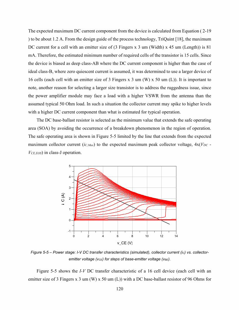
120
The expected maximum DC current component from the device is calculated from Equation ( 2-19
) to be about 1.2 A. From the design guide of the process technology, TriQuint [18], the maximum
DC current for a cell with an emitter size of (3 Fingers x 3 um (Width) x 45 um (Length)) is 81
mA. Therefore, the estimated minimum number of required cells of the transistor is 15 cells. Since
the device is biased as deep class-AB where the DC current component is higher than the case of
ideal class-B, where zero quiescent current is assumed, it was determined to use a larger device of
16 cells (each cell with an emitter size of 3 Fingers x 3 um (W) x 50 um (L)). It is important to
note, another reason for selecting a larger size transistor is to address the ruggedness issue, since
the power amplifier module may face a load with a higher VSWR from the antenna than the
assumed typical 50 Ohm load. In such a situation the collector current may spike to higher levels
with a higher DC current component than what is estimated for typical operation.
The DC base-ballast resistor is selected as the minimum value that extends the safe operating
area (SOA) by avoiding the occurrence of a breakdown phenomenon in the region of operation.
The safe operating area is shown in Figure 5-5 limited by the line that extends from the expected
maximum collector current (iC,Max) to the expected maximum peak collector voltage, 4x(VDC -
VCE,EOS) in class-J operation.
Figure 5-5 – Power stage: I-V DC transfer characteristics (simulated), collector current (iC) vs. collector-
emitter voltage (vCE) for steps of base-emitter voltage (vBE).
Figure 5-5 shows the I-V DC transfer characteristic of a 16 cell device (each cell with an
emitter size of 3 Fingers x 3 um (W) x 50 um (L)) with a DC base-ballast resistor of 96 Ohms for
2 4 6 8 10 120 14
0
1
2
3
4
-1
5
v_CE (V)

121
each cell. This ballast resistor is placed in the DC path to prevent current hogging among different
cells of the overall transistor.
It should be noted that the device behaves differently under RF operation than DC operation.
Effects, such as transient junction heating, occur under DC operation and does not occur under RF
operation. The safe operating area (SOA) under RF operation is usually larger than what is
estimated based on the DC curves. Therefore, estimating the base-ballast resistor based on the DC
curves is considered a conservative estimation.
The DC base-ballast resistor is added in the DC path between the power transistor and the bias
circuit as a part of the bias resistor (RB,Bs,1), as shown in Figure 5-7. To improve linearity while
avoiding a degradation of the power gain, it was elected to use a very small resister in the RF path
in the power stage, since any loss in the RF path degrades the power gain.
5.3.1.2–OutputMatchingNetwork–Class‐JLoad
Targeting class-J operation, from the analysis in Section 2.3.2.2, the optimum load of class-J is
determined in terms of the optimum load of ideal class-B (RL1,B) as
, , ,
, 1.179 ∗ , ( 5-7 )
Assuming ideal class-B operation, since the required maximum output power of the fundamental
frequency at the collector is 34.5 dBm (2.818 Watt), the corresponding output 1dB compression
point (O1dB) is estimated to be about 32.5 dB (1.78 Watt). For the given HBT transistor edge of
saturation voltage (VCE,EOS) is about 0.5 V, and the DC supply voltage is 3.5 V, the corresponding
iC,Max at the O1dB compression point is calculated from Equation ( 5-5 ) to be 2.37 A. From
Equation ( 2-18 ), the corresponding maximum amplitude of the fundamental current component
(Ic1,Max,B) is 1.185 A. From the analysis in Section 2.2.2, the optimum load for class-B is found as
, ,,
, ,
( 5-8 )
where Vce1,Max is the maximum amplitude of the fundamental voltage component, which equals
(VDC - VCE,EOS). The Ic1,Max,B is the maximum amplitude of the fundamental current component.

122
From Equation ( 2-15 ), RL1,B = 2.53 Ohm. From Equation ( 2-58 ), the estimated load for class-J
is
, 2.53 2.53
, 2.98 ( 5-9 )
It should be noted that the estimated load is calculated by assuming that the O1dB compression
point occurs at the maximum swing of the fundamental voltage and current components.
Biasing the power transistor as deep class-AB causes the second-harmonic current component
to be lower than the case of class-B. The load impedance of class-J is estimated based on ideal
class-B. Hence, the load impedance of the second-harmonic component should increase compared
to the estimated value in Equation ( 5-9 ) to compensate for the lower second-harmonic current
component in order to obtain the same second-harmonic voltage component level.
The output matching network is implemented as three sections where the only on-chip
component is the shunt capacitor and the rest of the network is off-chip, as shown in Figure 5-6.
Z_T3
RFC
R_L
On‐Chip Off‐Chip
Figure 5-6 – Output matching network.

123
Since the power stage is designed as class-J where no second-harmonic trap exists at the
collector terminal, each shunt branch of the off-chip network contains a shunt capacitor in series
with an inductance to create a notch in the frequency response (one notch at the second harmonic
frequency and the other at about the forth harmonic) in order to attenuate the harmonics and meet
emission specifications.
Applying the 10:1 rule of thumb of the RF path to the non-RF path impedance, the RF choke
value is selected such that the impedance of the choke approximately equals ten times the
impedance presented at the RF choke node. The RF choke should be connected to the matching
network at the node with the lowest impedance within the network. Such an approach provides the
smallest inductance of the choke with the smallest footprint on the laminate.
The matching network is initially designed to present the optimum load impedance of ideal
class-B, then it was tuned to present the required load for class-J operation. Such an approach was
found to be simple in obtaining the required load of class-J.
5.3.1.3–BiasCircuit‐LinearityEnhancement
Section 3.5.1 showed that an HBT transistor suffers from a bias depression phenomenon that
degrades the linearity at high input drive levels. The modified double diode-connected transistors
bias circuit, which was introduced by Noh and Park [49] and presented in Section 3.5.2, is utilized
in the design to provide a temperature compensation as well as a reduction to the bias depression
of the power transistor. The bias circuit has been modified by adding a resistor in series with the
two diode-connected transistors in the reference branch, as shown in Figure 5-7.
To determine the quiescent bias point, after selecting the power transistor size and the base-
ballast resistor, and presenting the estimated load impedance at the collector, a DC voltage source
is applied at the base. Both the load impedance and the base DC voltage are tuned for the highest
efficiency and the best linearity. Applying the bias level as a voltage source was found to be more
effective than applying it as a current source which is the typical approach in small-signal
amplifiers. The exponential relationship between the collector current (iC) and the base-emitter
voltage (vBE) can be approximated as a piecewise linear relationship as shown in Figure 5-8. From
the figure, a small change of current on segment “A” causes a large change of voltage. While, on
segment “B”, a small change of voltage causes a large change of current. Therefore, it is preferred
to bias the device with a current source when the bias point lies on segment “B” and to bias the

124
device with a voltage source when the bias point lies on segment “A”. For deep class-AB bias, the
device is approximately biased on segment “A”. Therefore, it was selected to apply a voltage
source at the base terminal.
R_B,Bs_1
V_Reg_1
R_Ref_1
V_Batt
Tothebaseterminal
ReferenceBranch
Figure 5-7 – Power stage bias circuit.
Figure 5-8 – Approximated piecewise linear curve of collector current (iC) vs. base-emitter voltage (vBE).

125
The base DC current of the emitter–follower transistor is related to the base DC current of the
power transistor by beta of the transistor (β) (for the given process, β = 80). The size of the emitter-
follower transistor is estimated from the following relationship
,, ( 5-10 )
where AT,EF is the emitter area of the emitter-follower transistor. The AT,PS is the emitter area of the
power transistor. For the selected power transistor of 16 cells (with emitter size of 3 Fingers x 3
um (W) x 50 um (L)) and the given beta, the emitter-follower transistor size can be estimated as 1
cell (with emitter size of 3 Fingers x 3 um (W) x 10 um (L)). It should be noted that in order to
avoid process variation affecting the bias circuit performance, it was elected to keep the minimum
width of each finger as 3 um and the minimum length of each finger as 15 um, for all transistors
in the bias circuits.
The initial bias resistor was selected to satisfy the rule of thumb of the RF to non-RF path
impedances. The bias resistor was divided into two parts: one part which is the DC base-ballast
resistor and the other part is added at the bias circuit such that the total resistance approximately
equals 10 times the small-signal input impedance of the transistor (determined by simulation).
Given the bias resistor value and the base bias current of the power transistor, the needed
reference voltage at the reference branch is determined where the reference branch is acting as a
voltage regulator. The reference branch was designed such that it provides the required voltage
and current while it consumes less DC current than the emitter–follower transistor to reduce the
current driven from the regulated supply voltage (VReg) and improve the total efficiency of the
power stage. It was elected to reduce the area of the diode-connected transistors by a factor of three
compared to the emitter-follower transistor in order to reduce the DC current while maintaining a
suitable transistor size that overcomes any process variation.
The impedance of the shunt capacitor is estimated, at the fundamental frequency (the center
of the targeted bandwidth), to approximately equal the input impedance of the reference branch at
the quiescent bias point. As the input drive signal increases, the DC current increases and the input
impedance of the reference branch decreases, causing the resultant parallel impedance of the
reference branch and the shunt capacitor to decrease faster. As a result, a larger portion of the RF

126
power leakage is applied to the emitter-follower transistor, forcing it into a bias depression that
compensates the bias depression of the power transistor.
5.3.2–DriverStageDesign
The design of the driver stage focused on providing the required output power to drive the power
stage up to the saturated output power level while maintaining the required linearity at back-off
power levels. Hence, the driver stage was designed such that it operates at the maximum linear
output power when the power stage is operating at the saturated output power level. Such an
approach was found to improve linear operation of the entire module.
For investigations, the driver stage was assumed to operate either as class-J or deep class-AB.
The initial design of the driver stage did not include a feedback. Later during the design process,
after integrating both the power stage and the driver stage with the electromagnetic (EM) model
of the ground inductance, the driver stage required a feedback loop for stability and it was elected
to operate the driver stage as deep class-AB to simplify the inter-stage matching network.
5.3.2.1–TransistorSizeandDCBallastResistor
The simulation of the power stage, as a separate stage, has shown about 15 dB of power gain at
the saturated output power level. Hence, the driver stage is required to provide a maximum linear
output power level of about 20 dBm. For marginal performance, it was assumed that the required
output power at the collector terminal is 21 dBm (0.126 Watt). The same steps discussed in Section
5.3.1.1 has been followed to estimate the transistor size and the required base-ballast resistor.
Either case of operating the driver stage as class-J or deep class-AB requires biasing the
transistor as deep class-AB (ideal class-B). For the given process technology, the HBT transistor
at low collector current exhibits an edge of saturation voltage (VCE,EOS) about 0.4 V. The DC supply
voltage is 3.5 V. The needed iC,Max is calculated from Equation ( 5-5 ) to be 162.5 mA.
For ideal class-B operation, the expected maximum DC current component from the device is
calculated from Equation ( 2-19 ) to be about 81.25 mA. From the design guide of the process
technology, the maximum DC current for a cell (with an emitter of size 3 Fingers x 3 um (W) x 45
um (L)) is 81 mA. The estimated number of required cells is 2 cells (each cell with an emitter size
of 3 Fingers x 3 um (W) x 50 um (L)). Such an estimation assumes the device is biased as a deep
class-AB where the DC current component is expected to be higher than the case of ideal class-B.
It is important to note that, another reason for selecting a larger size transistor is to account for the

127
ruggedness issue. Although the driver stage does not face a direct high VSWR load as the case of
the power stage, any change of the power stage load is reflected at the collector of the driver stage
since the power transistor is not a perfect unilateral device.
The DC base-ballast resistor is selected as the minimum value that extends the safe operating
area (SOA) by avoiding the occurrence of a breakdown phenomenon in the region of operation, as
discussed in Section 5.3.1.1. The safe operating area is shown in Figure 5-9 limited by the line that
extends from the expected maximum collector current (iC,Max) to the expected maximum peak
collector voltage, 4x(VDC - VCE,EOS) in class-J operation. Figure 5-9 shows the I-V DC transfer
characteristic of a 2 cell device (each cell with an emitter size of 3 Fingers x 3 um (W) x 50 um
(L)) with a base-ballast resistor of 90 Ohms for each cell.
Figure 5-9 – Driver stage: I-V DC transfer characteristics (simulated), collector current (iC) vs. collector-
emitter voltage (vCE) for steps of base-emitter voltage (vBE).
The DC base-ballast resistor is added in the DC path between the driver transistor and the bias
circuit as a part of the bias resistor, as shown in Figure 5-11. Also, a series resistor was added in
the RF path for both linearity and stability reasons.
It should be noted that the final transistor size was selected to be 3 cells (each cell with an
emitter size of 3 Fingers x 3 um (W) x 50 um (L)). The increase of the size was necessary to reduce
the power gain of the stage to improve the stability.

128
5.3.2.2–Inter‐StageMatchingNetwork–DeepClass‐ABLoad
In order to simplify the inter-stage matching network design, the driver stage was designed to
operate as deep class-AB (ideal class-B). For ideal class-B operation, the required output power of
the fundamental frequency at the collector is 21 dBm (0.1625 Watt). From Equation ( 2-18 ), the
maximum amplitude of the fundamental current component (Ic1,Max,B) is 81.25 mA. From Equation
( 2-15 ), for the given DC supply voltage of 3.5 V and the edge of saturation voltage of about 0.4
V, the estimated load is RL1,B = 38.2 Ohm.
It should be noted that since deep class-AB operation exhibits a higher level of the
fundamental current component than ideal class-B, the load should be decreased lower than the
estimated load. Also, it was observed during the design process that in order to obtain a good level
of linearity, the load may need to decrease than the estimated value.
The inter-stage matching network is implemented as a single-section L-network, as shown in
Figure 5-10. The series capacitor is implemented on the die to function as a DC block between the
two stages while being a part of the impedance-transforming network. The shunt indicator is
implemented on the laminate to obtain a high quality factor while acting as an RF choke.
V_DC2
Figure 5-10 – The inter-stage matching network.
Such a simple topology has been proved to be effective in presenting the needed load to the
transistor while occupying a small die area. It is important to note that although the inter-stage
matching network is seen as a high-pass network of a series capacitor and a shunt inductor, the
network behaves as a band-pass network since the input impedance of the power transistor includes
shunt capacitors, Lu, et al. [59], providing a low impedance at the harmonics.

129
5.3.2.3–BiasCircuit‐LinearityEnhancement
In order to provide temperature compensation, the double diode-connected transistors bias circuit
was utilized in the driver stage. Also, a shunt capacitor at the base of the emitter-follower transistor
is added to reduce the bias depression of the driver transistor, as shown in Figure 5-11.
R_B,Bs_2
V_Reg_2
R_Ref_2
V_Batt
Tothebaseterminal
ReferenceBranch
Figure 5-11 – Driver stage bias circuit.
The same steps discussed in Section 5.3.1.3 have been followed to determine the quiescent
bias point, where a voltage source was applied at the base terminal and the base bias voltage that
gave best linearity was selected. To determine the size of the emitter-follower transistor, a lower
beta (β = 50) was estimated since the driver stage operates at a much lower DC collector current.
From Equation ( 5-10 ), for the selected driver transistor of 3 cells x (with an emitter size of 3
Fingers x 3 um (W) x 50 um (L)) and the given beta, the emitter-follower transistor can be
estimated as 1 cell (with an emitter size of 1 Finger x 3 um (W) x 9 um (L)). Though, it was
selected to use a transistor of 1 cell (with an emitter size 1 Finger x 3 um (W) x 15 um (L)) to
avoid process variations affecting the bias circuit performance.
The bias resistor was selected to satisfy the 10:1 rule of thumb of the RF to non-RF path
impedances. The bias resistor was divided into two parts: one part is the DC base-ballast resistor
and the other part is added at the bias circuit such that the total resistance approximately equal to
10 times the small-signal input impedance of the driver transistor (determined by simulation).

130
Given the bias resistor value and the base bias current of the driver transistor, the reference
voltage at the reference branch is determined. A ratio of one was used between the emitter-follower
transistor and the transistors of the reference branch since the smallest size recommended to avoid
process variation effects has been used in the emitter-follower transistor.
The impedance of the shunt capacitor value is estimated at the fundamental frequency (the
center of the targeted bandwidth). The estimation is set to approximately equal the input impedance
of the reference branch at the quiescent bias point.
5.3.2.4–InputMatchingNetwork
The input matching network was designed as a single-section T-network using the design
equations introduced in Section 4.2.2.1. The network provides a conjugate match to the input
impedance of the driver stage from the source impedance, which is typically 50 Ohms. Figure 5-12
shows the input matching network topology.
R_STothebaseterminal
Figure 5-12 – The input matching network.
The network topology was selected such that an inductor is in series with the base terminal of
the driver transistor. The topology intended to further stabilize the driver stage and maintain that
stabilization over process variations of both the die and the laminate. The concept is, the inductor
exhibits a low quality factor (about 7) and a high loss, the inductor loss that is in series with the
base terminal of the driver transistor would force the total impedance around the loop at the base
node to be positive. It is important to note that such a technique does not cause a significant
degradation in the power gain of the driver stage since the input impedance of the driver transistor
is much higher than the inductor loss.

131
It should be noted that the inductance of the input trace on the module laminate has been
resonated out by the input matching network on the die to obtain 50 Ohms at the input pin of the
module.
5.3.2.5–FeedbackLoopandEmitterDegenerationforStability
The ground inductance of both the power stage and the driver stage creates a feedback path
between the two stages. That feedback path may cause the driver stage to oscillate. Two techniques
can be utilized to stabilize the driver stage. One is using a feedback loop, typically a resistor in
series with a DC blocking capacitor, between the collector and base terminals. Another technique
is to add an emitter inductance degeneration, which is a small inductance in series with the emitter
terminal. The concept of the emitter inductance degeneration is to increase the isolation between
the driver stage and the power stage, reducing the feedback between the two stages. It should be
noted that the emitter inductance improves the noise performance of the power amplifier as well,
Lin, et al. [60]. Both techniques were utilized in the design, as shown in Figure 5-13.
V_DC2
RFC
R_FB
L_Stab
R_Lin,2
Figure 5-13 – A Feedback loop and an emitter inductance degeneration for stabilizing the driver stage.
It is important to note that both techniques cause a reduction in the power gain of the driver
stage. Therefore, it is important to start the design with a high power gain. The 10:1 rule of thumb
used throughout the design was applied to choose the initial value of the feedback resistor where

132
it was chosen to satisfy 10 times the small-signal input impedance of the driver transistor including
the linearization resistor (RLin,2) in the RF path.
5.4–TheDesignSchematicandLayout
5.4.1–FullModuleSchematic
A detailed schematic of the implemented power amplifier module is shown in Figure 5-14.
RF_in
V_DC
RF_out
V_Batt
BiasCircuit1
V_DCV_Batt
BiasCircuit2
RFC
ModuleLaminate
GaAsHBTDie
Figure 5-14 – The full schematic of the power amplifier module.
Figure 5-14 identifies the portion of the module that was implemented on the die and the other
portion on the laminate. It is important to note that a bypass capacitor is added on each DC supply
trace (VDC, and VBatt) to avoid an RF leakage and feedback paths from the DC supply side. The
bypass capacitors are not shown in Figure 5-14.
5.4.2–PowerAmplifierDieLayout
One goal of the design is to reduce the area needed for the power amplifier die to achieve a low
cost while maintaining high performance. Figure 5-15 shows the final layout of the taped-out die.
It should be noted that the required die area is much less than the physical dimensions of the taped-
out die (710 um x 790 um, not including saw street dimensions). The dimensions of the taped-out
die was maintained to fit the die with other circuits in a quadrant.

133
PowerStage
DriverStage
BiasCircuit1
BiasCircuit2
InputMatchingNetwork
RFin
RFout
Figure 5-15 – The layout of the GaAs HBT die.
Important considerations maintained during the layout phase:
Maintaining a symmetry in the device layout for each cell and the associated
components, such as DC base-ballast resistors and matching network capacitors is
important to avoid current hogging during operation as the device temperature
increases.
The reference branch of the bias circuit is kept in a very close proximity to the
associated power/driver transistor to enable the bias circuit to effectively track the
temperature variations of the power/driver transistor.
Figure 5-16 shows a photograph of the taped-out GaAs die (bump-pillars are pointing up).
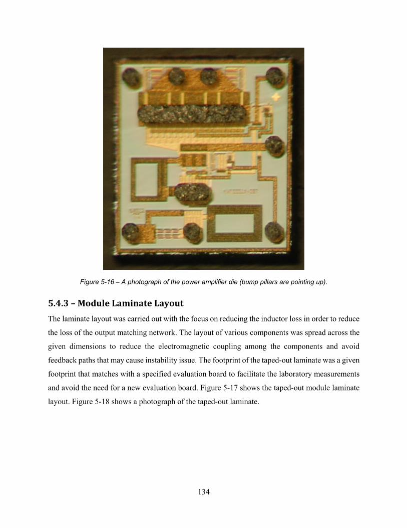
134
Figure 5-16 – A photograph of the power amplifier die (bump pillars are pointing up).
5.4.3–ModuleLaminateLayout
The laminate layout was carried out with the focus on reducing the inductor loss in order to reduce
the loss of the output matching network. The layout of various components was spread across the
given dimensions to reduce the electromagnetic coupling among the components and avoid
feedback paths that may cause instability issue. The footprint of the taped-out laminate was a given
footprint that matches with a specified evaluation board to facilitate the laboratory measurements
and avoid the need for a new evaluation board. Figure 5-17 shows the taped-out module laminate
layout. Figure 5-18 shows a photograph of the taped-out laminate.

135
PADie
OutputMatchingNetwork
RFC
RFin
RFout
Figure 5-17 – The layout of the module laminate.
Figure 5-18 – A photograph of the module laminate.

136
5.5–SimulationandExperimentalResults
5.5.1–SimulationStrategy
The power amplifier module design required integrating multiple technologies in a single package.
The module integrated a GaAs HBT die that represents the power amplifier circuit, and an external
output matching network on the laminate. The shunt inductor of the inter-stage matching network,
which also acts as an RF choke, was implemented as a printed inductor on the laminate for a lower
loss. Surface Mount Technology (SMT) capacitors were integrated on the module as components
of the matching network and bypass capacitors on each DC supply voltage. The bypass capacitors
are needed to shunt the RF signal to ground, preventing RF signal leakage to the external system.
The strategy of the simulation was to combine both schematic models and simulated
electromagnetic models in a single schematic simulation. The GaAs HBT transistor models in the
available design kits from TriQuint were used in the schematic of the power amplifier, TriQuint
[61]. All on-chip inductors were implemented by performing an electromagnetic simulation to
determine the inductor value and the associated loss, as shown in Figure 5-19. To reduce the
inductor loss, all on-chip spiral inductors were designed by stacking metal1, via1, and metal2 as a
single conductor of the inductor.
Figure 5-19 – EM simulation for S-parameters of an on-chip spiral inductor.

137
The design of the output matching network started from a schematic where the loss of the
inductor was included. The implementation of each inductor on the laminate was performed
through an iterative electromagnetic simulation to determine the inductance value and the
associated loss, as shown in Figure 5-20. To maintain a high quality factor of the printed inductors
on the laminate, the printed inductors were restricted to the top two metal layers of the laminate
(metal1 and metal2) where both metal layers were integrated to construct the inductor. The SMT
capacitor models, obtained from Murata [62], were integrated with the simulated electromagnetic
model of the matching network during schematic simulations of the matching network and the full
power amplifier module.
Figure 5-20 – EM simulation for S-parameters of a printed Inductor on the laminate.
Implementing the power amplifier die in a flip-chip technology presented a challenge during
the simulation of the design. Determining the ground inductance of the die was found to be critical
to evaluate many of the power amplifier characteristics such as power gain, efficiency and stability.
Determining the inductance of the bump pillars connected to the output matching network are
critical to estimate the load impedance presented to the power transistor at the collector terminal.
Electromagnetic simulations were necessary to estimate both the ground inductance and the bump-
pillar inductance in each case.

138
At the final phase of the design, a full electromagnetic simulation was performed for the entire
module laminate in order to capture any coupling or feedback paths through the laminate, as shown
in Figure 5-21. The generated EM model (contains S-parameters) of that simulation was combined
with the schematic of the power amplifier die and the SMT capacitors model to create a full
simulation of the entire module.
Figure 5-21 – EM Simulation for S-parameters of the full module laminate.
5.5.2‐SimulationResults
“Advanced Design System” (ADS) software, from Keysight [63] (formerly Agilent [64]), was
used in both schematic and electromagnetic simulations. The “Harmonic Balance” simulator,
which is a nonlinear simulator, was the main simulation engine utilized in evaluating the power
amplifier large-signal characteristics, such as power gain, phase difference, and power efficiency.
Small-signal “S-Parameters” was used to simulate the passive sections of the module such as the
matching networks. Momentum-Microwave was the engine used for all electromagnetic
simulations to obtain the S-parameters.
All harmonic balance simulations were based on applying a single-tone drive signal
representing a continuous wave (CW). Due to limitations in the available licenses, no modulated
signal was utilized during simulations. During the design process, the evaluation of the power
amplifier linear operation was fully based on achieving highly linear AM-AM and AM-PM curves.

139
5.5.2.1–LoadImpedance
The final load impedance of the power stage of the taped-out die and laminate is shown in Figure
5-22. It is important to note that the reactive part of the fundamental load impedance is lower than
the estimated value of class-J load in Section 5.3.1.2. Such a deviation was intentionally employed
to reduce the peak value of the collector voltage. The initial design caused the peak value to exceed
12 V. Although the GaAs HBT transistor in the given process exhibits a collector-emitter
breakdown voltage (BVCEO) of 14 V, it was elected to reduce the peak value to lower than 10 V as
shown in Figure 5-23. The reduction of the peak value was targeted as a precaution to avoid
ruggedness issue during laboratory measurements if the module was exposed to a high VSWR.
Also, due to the fact that the design is the first to utilize a GaAs HBT process in the implementation
of class-J which causes a much higher non-typical peak value of the collector voltage compared to
deep class-AB and class-F operation.
Figure 5-22 – The simulated load impedance (real and imaginary parts) of the power stage.
Re{
Z}
(Ohm
)
Im{Z
} (O
hm)
Re{
Z}
(Ohm
)
Im{Z
} (O
hm)

140
Figure 5-23 – The collector current and voltage waveforms of the power stage.
Figure 5-24 shows the load impedance presented to the driver stage. As discussed in Section
5.3.2, the driver stage was designed to operate as deep class-AB.
Figure 5-24 – The simulated load impedance (real and imaginary parts) of the driver stage.
i_C
(A
) v_C (V
)

141
5.5.2.2–Linearity
During the design phase, the evaluation of linear operation was based on both the power gain
linearity (AM-AM) and the phase difference between the output and input signals (AM-PM). Figure
5-25 shows the power gain of the entire module vs. the output power at the center frequency of the
bandwidth (865 MHz), and the band edges (815MHz and 915 MHz). Figure 5-26 shows the phase
difference between the output and input signals vs. the output power at the same three frequencies.
Figure 5-25 – The simulated power gain vs. output power at f0 (frequencies 815, 865, and 915 MHz).
Figure 5-26 – The simulated phase difference between output and input signals vs. output power at f0
(frequencies 815, 865, and 915 MHz).
22 24 26 28 30 32 3420 36
100
120
140
160
80
180
Pout (dBm)
815 MHz
865 MHz
915 MHz

142
From the figures, the power amplifier module maintained a power gain variation of less than
0.5 dB and a phase difference variation of about 10o across a 10 dB of varying output power range.
Typically, maintaining such a low variation of both power gain and phase difference within the
varying output power region results in high linearity in terms of Adjacent Channel Power Ratio
(ACPR) and Error Vector Magnitude (EVM) test specifications.
5.5.2.3–PowerEfficiency
The power efficiency and power-added efficiency (PAE) were evaluated through equations using
the power levels and DC current components that resulted from the harmonic balance simulations.
Figure 5-27 shows the power-added efficiency, at the center frequency of the bandwidth (865
MHz), and the band edges (815 MHz and 915 MHz). The figure shows the power-added efficiency
exceeds 62% which represents an improvement of 7% above the typical power-added efficiency
offered by the industry (about 55% maximum).
Figure 5-27 – The simulated power added-efficiency vs. output power at f0 (frequencies 815, 865, and
915 MHz).
5.5.3–MeasurementResults
To evaluate the performance of the implemented power amplifier module, the module was
assembled and soldered to an evaluation board, as shown in Figure 5-28. All tests were performed
using an automated test bench, in room temperature, and with a 50 Ohm load (VSWR = 1). The
loss of the RF input/output traces of the evaluation board were measured and de-embedded from

143
the measurement results in order to reference the results to the module boundary. The same test
environment was maintained for all tests, as shown in Figure 5-29.
Figure 5-28 – The fully assembled power amplifier module on evaluation board for testing.
SignalGenerator
V_BattSupply
V_DCSupply
SpectrumAnalyzer
DeviceUnderTest
PowerMeter
RF_in RF_out
Figure 5-29 – A block diagram of the test environment.
The module was tested in different modes of operation (2G/GSM, 2.5G/EDGE, and 3G/W-
CDMA)23. The test of each mode was carried out by applying a modulated input signal that
23 - Due to a limitation of the available modulated signals, the 4G/LTE mode was not tested.

144
matches the requirements of each standard. The input power level of the modulated signal was
swept up to the level that generates the specified maximum output power for each mode. The
measurements were repeated at different frequencies within the targeted bandwidth (815 MHz –
915 MHz), which covers bands 5, 6, 8, 18, 19, 20, 26 of the cellular spectrum, 3GPP [40]. The test
environment settings are summarized in Table 5-2.
VDC 3.5 V VBatt 3.5 V
Load - VSWR 50 Ohm – (VSWR = 1) Temperature Room Temp. = 25 oC
Frequency Points 815, 824, 836, 849, 862, 880, 900, 915 (MHz)
2G/GSM: Input Power (PIN) Sweep Range -10 dBm – 10.5 dBm 2.5G/EDGE: Input Power (PIN) Sweep Range -20 dBm – 1 dBm
3G/W-CDMA: Input Power (PIN) Sweep Range -20 dBm – 1 dBm
Table 5-2 – Test environment settings.
The automated test bench measured the output power at the fundamental frequency (f0) and
the harmonics, the DC current, and linearity measurements such as Adjacent Channel Power Ratio
(ACPR) and Error Vector Magnitude (EVM) tests.
It should be noted that three different modules were assembled and tested, where the results
of the three modules came out in a very good agreement.
5.5.3.1–2G/GSMMode
The measurements of the 2G/GSM mode was performed by applying a continuous wave (CW)
signal to the power amplifier module. The GSM signal utilizes Gaussian Minimum Shift Keying
(GMSK) modulation which generates a constant envelope signal. The main characteristics that
were evaluated are the power gain, the power-added efficiency (PAE), and the second harmonic
power level vs. the output power at the fundamental frequency (f0). Figure 5-30 - Figure 5-32 show
the measurement results of those characteristics respectively.

145
Figure 5-30 – 2G/GSM: The measured power gain vs. output power at f0 (multiple frequencies).
Figure 5-31 – 2G/GSM: The measured power-added efficiency (PAE) vs. output power at f0 (multiple
frequencies).
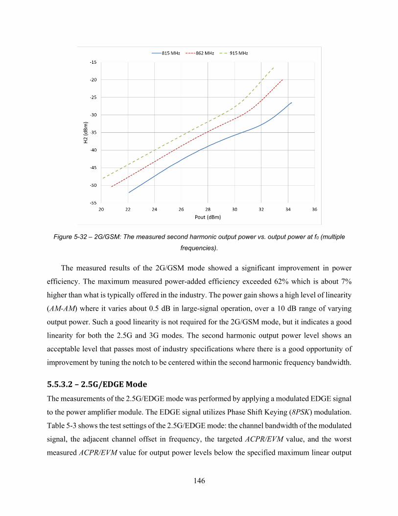
146
Figure 5-32 – 2G/GSM: The measured second harmonic output power vs. output power at f0 (multiple
frequencies).
The measured results of the 2G/GSM mode showed a significant improvement in power
efficiency. The maximum measured power-added efficiency exceeded 62% which is about 7%
higher than what is typically offered in the industry. The power gain shows a high level of linearity
(AM-AM) where it varies about 0.5 dB in large-signal operation, over a 10 dB range of varying
output power. Such a good linearity is not required for the 2G/GSM mode, but it indicates a good
linearity for both the 2.5G and 3G modes. The second harmonic output power level shows an
acceptable level that passes most of industry specifications where there is a good opportunity of
improvement by tuning the notch to be centered within the second harmonic frequency bandwidth.
5.5.3.2–2.5G/EDGEMode
The measurements of the 2.5G/EDGE mode was performed by applying a modulated EDGE signal
to the power amplifier module. The EDGE signal utilizes Phase Shift Keying (8PSK) modulation.
Table 5-3 shows the test settings of the 2.5G/EDGE mode: the channel bandwidth of the modulated
signal, the adjacent channel offset in frequency, the targeted ACPR/EVM value, and the worst
measured ACPR/EVM value for output power levels below the specified maximum linear output

147
power. Figure 5-33 and Figure 5-34 show the measured ACPR-200, and EVM, respectively, vs.
output power level at the fundamental frequency (f0).
ACPR-200 ACPR-400 EVM Channel Bandwidth 30 KHz
Adjacent Channel Offset ± 200 KHz ± 400 KHz - Targeted -33 dBc -50 dBc 3 %
Measured (worst) -34.2 dBc -53 dBc 3 %
Table 5-3 – 2.5G/EDGE: test settings.
Figure 5-33 – 2.5G/EDGE: The measured ACPR-200 (worst of upper/lower) vs. output power at f0
(multiple frequencies).
The measured results of the 2.5/EDGE mode shows a good linearity operation within the
varying output power region that passes most industry specifications.

148
Figure 5-34 – 2.5G/EDGE: The measured EVM vs. output power at f0 (multiple frequencies).
5.5.3.3–3G/W‐CDMAMode
The measurements of the 3G/W-CDMA mode was performed by applying a Release-99 (GTC1)
modulated signal to the power amplifier module. The W-CDMA signal utilizes a Hybrid Phase
Shift Keying (HPSK) modulation. Table 5-4 shows the test settings of the 3G/W-CDMA mode:
the channel bandwidth of the modulated signal, the adjacent channel offset in frequency, the
targeted ACPR value, and the worst measured ACPR value for output power levels below the
specified maximum linear output power. Figure 5-35 shows the measured ACPR1 vs. output power
level at the fundamental frequency (f0).
ACPR1 ACPR2 Channel Bandwidth 3.84 MHz
Adjacent Channel Offset ± 5MHz ± 10 MHz Targeted value -33 dBc -43 dBc Measured value -34.9 dBc -50 dBc
Table 5-4 – 3G/W-CDMA: test settings.

149
Figure 5-35 – 3G/W-CDMA: The measured ACPR1 (worst of upper/lower) vs. output power at f0 (multiple
frequencies).
The measured results of the 3G/W-CDMA mode shows a good linearity operation that passes
most industry specifications.
5.5.4–Discussion
Both the measurement and simulation results show that the implemented power amplifier module
achieved the target of operating with high efficiency in the 2G/GSM mode while operating with
high linearity that meets the industry specifications in the 2.5G/EDGE and 3G/W-CDMA modes,
[3GPP [40]]. Such a successful design validates the proposed design techniques.
The implemented design showed a significant improvement of efficiency in the 2G/GSM
mode as it exceeds what is typically offered in the industry by 7%. Also, at back-off power levels,
the power-added efficiency is enhanced where at the maximum linear output power it reaches
above 35%. Such an improvement is due to the implementation of class-J in the design as the
technique to improve the power efficiency.
The measurement results of the second harmonic output power level showed the success of
the proposed design methodology in Chapter 4. The implemented design achieved better results

150
using an off-chip two-section matching network compared to what is typically used in the industry
where an off-chip three-section matching network is utilized.
The linearity measurements (ACPR and EVM) in the 2.5G and 3G modes showed a high
linearity that passes industry specifications. Such a good linearity is due to the application of
multiple concepts at the input section of each stage (power stage and driver stage) where a bias
circuit is employed for temperature compensation and bias depression reduction. Also, both the
input matching network and the output impedance of the bias circuit were used as a tuning knobs
to improve linearity. Although the 4G/LTE mode was not tested, the results of the 3G mode
indicates that the power amplifier can pass 4G/LTE specifications.
It is important to note that the presented measured results represent a first-pass design (first
tape-out of both the PA die and the module laminate) with no tuning of the circuit in the laboratory.
The measured results shows a very good agreement with the simulation results. Such an agreement,
with no tuning of the circuit in the laboratory, highlights the necessity of integrating the
electromagnetic (EM) simulations within the schematic simulations, which was the strategy taken
during the simulation phase of the design (before the tape-out) as presented in Section 5.5.1. The
simulation strategy gains importance as the operating frequency increases since the probability of
coupling and the occurrence of feedback paths increase as frequency increases.
It should be noted that the load impedance of the implemented design was modified to exhibit
a slope across the targeted bandwidth rather than a flat load impedance that achieves a broadband
response. The goal of such a deviation was to avoid the need for multiple tape-out variants of both
the PA die and the laminate, to reduce cost and resources. The strategy was to have a different load
at different frequencies. By sweeping the frequency, the optimum load can be determined. If a
second tape-out was available, the optimum load would have been implemented across the targeted
bandwidth to achieve the optimum performance across the entire bandwidth. The effect of the load
impedance variation across the bandwidth is clear where the power gain at low input drive levels
varies about 3 dB, as shown in Figure 5-30. The power-added efficiency (PAE) varies about 7%,
as shown in Figure 5-31. And, the ACPR also varies, as shown in Figure 5-33.
In conclusion, the measured results of the implemented power amplifier proved the success
of the proposed design techniques of a single power amplifier that operates with high efficiency in
one mode while the same amplifier with no modification operates with high linearity and enhanced
efficiency in another mode, providing a solution for the converged power amplifier architecture.

151
5.5.4.1–OpportunityforImprovements
Implementing the best load, from the measured results, across the entire bandwidth represents an
opportunity for improving the design performance across the entire bandwidth. Such a change
should reduce the large variations in power gain, power-added efficiency, ACPR, and EVM.
As discussed in Section 5.5.2.1, the final load impedance was reduced from the optimum load
impedance to avoid a ruggedness issue due to the high peak collector voltage that is inherited from
class-J. Increasing the load impedance back to the optimum load would achieve a higher efficiency
with the cost of higher peak collector voltage.
5.6–Summary
The proposed design process of a linear power amplifier with high efficiency was introduced in
this chapter. The design process relies on utilizing class-J as the technique of improving the power
efficiency while maintaining linear operation. In order to improve linearity, the bias circuit should
provide temperature compensation and reduction of the bias depression of the power transistor
where the output impedance of the bias circuit is controlled.
A design of a power amplifier module was implemented to validate the effectiveness of the
design process. Both simulated and measured results of the implemented module showed a good
agreement, highlighting the success of the proposed design process. The results showed the power
amplifier module operates in the 2G/GSM with high efficiency up to 62%, about 7% higher than
the industry. The power amplifier also operates in both the 2.5G/EDGE, and 3G/W-CDMA modes
with high linearity that meets the industry specifications.

152
(This page left intentionally blank)

153
6.
Conclusion
6.1–ResearchSummary
The major goal of the research was to develop design techniques for a linear power amplifier that
operates with high efficiency at the saturated output power level (in the 2G mode), operates with
high linearity and enhanced efficiency at back-off output power levels (in the 2.5G/3G/4G modes),
and covers a broadband frequency response. Such a power amplifier represents a solution to the
converged power-amplifier architecture in handsets, where a single power amplifier operates in
multiple modes (2G/2.5G/3G/4G), while covering one of the three major frequency bands in the
cellular spectrum (low band: 695 MHz – 915 MHz, mid band: 1710 MHz – 2025 MHz, or high
band: 2300 MHz – 2700 MHz).
To develop the design process, the research investigated three different areas of interest in the
power amplifier design. The three areas of interest are: achieving high power efficiency, operating
with high linearity, and covering a broadband frequency response.
Chapter 2 presented the current techniques of improving the power efficiency of a linear
power amplifier, deep class-AB and class-F. The main issue that impedes these techniques from
achieving the maximum theoretical power efficiency lies in the implementation part of the design.
In deep class-AB, presenting a non-perfect short-circuit at the harmonics, especially the second
harmonic, degrades the power efficiency, the output power, and the linearity. Such a situation
occurs when using a small shunt capacitor at the collector terminal rather than a second-harmonic
trap, or using a single second-harmonic trap rather than double second-harmonic traps in a
broadband design.
Also in Chapter 2, class-J operation was investigated in details where the optimum load, the
maximum power efficiency, and the maximum linear output power were derived. The analysis of
class-J was restricted to utilizing the second-harmonic component rather than the general
theoretical definition of class-J where the second and higher harmonic components are utilized.
Class-J has a few advantages making it suitable to the implementation of handset power amplifiers.
Class-J does not require a perfect short-circuit termination for the second harmonic, eliminating
the need for a second-harmonic trap at the collector terminal and avoiding the implementation

154
issues of deep class-AB. Class-J adds the second-harmonic voltage component in-phase to the
fundamental component which increases the minima of the voltage waveform away from the edge
of saturation voltage (VCE,EOS) avoiding operation in the saturation region of the transistor which
is a highly non-linear region. Therefore, class-J can achieve a higher practical power efficiency
than deep class-AB while maintaining a high linearity.
Chapter 3 presented a detailed discussion about the linearity in power amplifiers. Few of the
highlighted issues are: the nature of nonlinearity is categorized as weakly and strongly
nonlinearities; both the amplitude (AM-AM) and phase (AM-PM) distortions cause a waveform
distortion; and the operation with a reduced conduction angle exhibits a form of nonlinearity. The
transistor characteristics affect the linearity. The expansive transconductance of the HBT can be
utilized to reduce the nonlinearity inherited from the reduced conduction angle operation. Also,
the elimination of odd-degree harmonic components at the output of the transistor may improve
linear operation.
Additionally, in Chapter 3, investigations of techniques to linearize the relationship between
the collector current and the input voltage of an HBT were presented, such as using a series resistor
at the base terminal, while considering the effects of both the bias circuit output impedance and
the input matching network frequency response. Multiple bias circuits were discussed to obtain a
circuit that provides temperature compensation and reduces the bias depression phenomenon that
occurs in HBT power transistors at high output power levels.
Chapter 4 presented a new design methodology for broadband matching networks using
simple design equations of single-section networks (L and T-network) while incorporating the
inductor loss. The technique provides an accurate impedance transformation while adding more
degrees of freedom to the design process where the designer can determine the needed trade-off
among the out-of-band attenuation, the network loss and the network size.
The proposed design process of a linear power amplifier with high efficiency was introduced
in Chapter 5. The design process relies on utilizing class-J as the technique of improving the power
efficiency while maintaining linear operation. In order to improve linearity, a bias circuit that
provides both temperature compensation and a reduction of the bias depression of the power
transistor should be used.
A design of a power amplifier module was implemented to demonstrate the effectiveness of
the proposed design techniques. Both simulated and measured results of the implemented module

155
proved the success of the proposed design techniques. The results showed the power amplifier
module operates in the 2G/GSM mode with a high efficiency of up to 62%, about 7% higher than
what is typically offered in the industry. The power amplifier also operates in both the 2.5/EDGE,
and the 3G/W-CDMA modes with high linearity that meets the industry specifications. Though
the 4G/LTE mode was not tested, the results of the 3G mode indicated that the power amplifier
can pass 4G/LTE linearity specifications. The results showed the effectiveness of the new design
methodology of broadband matching networks as high harmonic attenuation was achieved using
only a two-section off-chip network compared to a three-section off-chip network that is typically
used in the industry.
6.2–Conclusion
The analysis, discussions, and investigations throughout the research demonstrated design
techniques for a linear power amplifier that operates with high efficiency and covers a broadband
frequency response. The design requires utilizing a technique to improve the efficiency, maintain
a high linearity, and avoids the implementation issues of the harmonic terminations that hinders
typical design techniques, such as deep class-AB.
Class-J showed a few advantages making it the proper technique to achieve high practical
efficiency at the saturated output power level while providing the needed linearity with enhanced
efficiency at back-off output power levels. Class-J utilizes the second harmonic component in
addition to the fundamental component to shape the collector voltage waveform such that the
minima of the voltage waveform increases away from the edge of saturation voltage (VCE,EOS),
avoiding operation in the saturation region of the transistor, which is a highly nonlinear region.
The implementation of class-J does not require presenting a short-circuit termination at the
second harmonic, avoiding the need for a second-harmonic trap, double second-harmonic traps for
broadband designs, or a larger capacitor at the collector terminal. In each case, a larger die size
would be needed and the practical deviation of presenting a perfect short-circuit termination causes
a degradation of the output power, the power efficiency and linear operation.
Class-J utilizes the second harmonic component compared to class-F that utilizes the third
harmonic component. For a given low-frequency process technology of a transistor, class-J is more
suitable than class-F to implement a power amplifier that covers a high frequency band.

156
The load impedance required for class-J consists of a combination of resistive and inductive
components at the fundamental frequency and a capacitive termination at the second harmonic
frequency. The implementation of such a load requires adding a shunt capacitor at the collector
terminal of the transistor and presenting an inductive impedance higher than what is typically
presented for deep-class-AB, before the shunt capacitor. Such an implementation is found to be
useful since the high inductive component acts as an RF choke for the harmonics, attenuating the
harmonics passing to the output matching network. Hence, the needed attenuation of the harmonics
by the matching network is reduced, and the network size can be reduced.
Restricting class-J operation to the utilization of the second harmonic component only, rather
than the general theoretical definition where the second and higher harmonics can be utilized,
improves the linearity as it avoids the odd-degree harmonic components which degrade linear
operation. Such a feature of class-J may improve the linearity compared to class-F which utilizes
the third harmonic component.
The research showed that the GaAs HBT process technology provides a suitable process to
implement the design of a linear power amplifier with high efficiency. GaAs HBT transistors
exhibit a high collector-emitter breakdown voltage (BVCEO), making it suitable to implement class-
J where the peak of the collector voltage waveform my reach up to four times the difference
between the DC supply voltage and the edge of saturation voltage (4 x (VDC - VCE,EOS)).
Employing GaAs HBT transistors in the design provides an opportunity to improve the
linearity further. HBT transistors show an expansive transconductance that reduces the
compressive nonlinearity that occurs due to the reduced conduction angle operation. Although
HBT transistors exhibit a strong nonlinear relationship between the collector current and the base-
emitter voltage due to the exponential relationship, adding a series resistor with the base terminal,
modifying the output impedance of the bias circuit, and considering the effect of the frequency
response of the input matching network may linearize the relationship between the collector
current and the input voltage of the amplifier. Improving the linearity of a power amplifier that
employs an HBT transistor requires implementing a bias circuit that reduces the bias depression
phenomenon of the HBT while providing temperature compensation.
The simulated and measured results proved the success of the proposed techniques for
implementing a linear power amplifier that operates with high efficiency at the saturated output
power level and maintains high linearity with enhanced efficiency at back-off output power levels.

157
6.3–SignificanceoftheResearch
The research investigated three major areas of interest for a power amplifier design: achieving a
high power efficiency, operating with a high linearity, and covering a broadband frequency
response.
The major significance of the research is developing design techniques for a linear power
amplifier that operates with high efficiency at the saturated output power level while providing the
needed linearity with enhanced efficiency at back-off output power levels and covering a
broadband frequency response.
The proposed design techniques are considered contributions to the current research efforts in
the handset power amplifier industry to develop a single multi-mode, multi-band power-amplifier
module. The proposed design process represents a solution to the converged power-amplifier
architecture where a single power amplifier can operate in different modes (2G/2.5G/3G/4G). The
proposed solution would eliminate at least two power amplifiers with the associated matching
networks from the current architecture in the industry, saving board area and cost, while improving
the performance. The power amplifiers that operate in the 2G/2.5G modes are the suggested
amplifiers to be eliminated, where the proposed design process achieved higher efficiency than
what is typically offered in the industry.
The research applied a new technique of achieving high power efficiency to the handset power
amplifier industry, which is class-J. Although class-J has been implemented for high-power
applications that are suitable to base stations using FET technology, it has not been implemented
in handsets. To our knowledge, the proposed development is the first attempt to realize class-J as
a handset power amplifier.
The research extended the implementation of class-J to a new process technology which is
GaAs HBT. Class-J has been implemented using GaN HEMT, Wright, et al. [28], and GaN FET,
Rezaei, et al. [30], process technologies. To our knowledge, the proposed design process is the
first implementation of class-J utilizing the GaAs HBT process technology.
One other significance is producing a new design methodology for broadband matching
networks. The methodology is valid to any matching network design (e.g., power amplifier, low
noise amplifier…). The methodology provides an accurate impedance transformation while adding

158
more degrees of freedom to the design process where the designer can determine the needed trade-
off among the out-of-band attenuation, the network loss, and the network size.
It is important to note that the implementation of the proposed design process is simpler than
the typical implementation of other techniques, such as deep class-AB or class-F. The proposed
process reduces the complexity of the matching network at the collector terminal by reducing the
required number of circuit elements.

159
Bibliography
[1] N. Cheng and J. P. Young, "Challenges and Requirements of Multimode Multiband Power
Amplifiers for Mobile Applications," in Compound Semiconductor Integrated Circuit
Symposium (CSICS), 2011 IEEE, 2011, pp. 1-4.
[2] E. McCune, "Advanced Architectures for High-Efficiency Multi-Mode, Multi-Band
Terminal Power Amplifiers," in Radio and Wireless Conference, 2004 IEEE, 2004, pp.
167-170.
[3] K. Daehyun, K. Dongsu, C. Jinsung, K. Jooseung, C. Yunsung, and K. Bumman, "A
Multimode/Multiband Power Amplifier With a Boosted Supply Modulator," Microwave
Theory and Techniques, IEEE Transactions on, vol. 58, pp. 2598-2608, 2010.
[4] F. H. Raab, "Class-F Power Amplifiers with Maximally Flat Waveforms," Microwave
Theory and Techniques, IEEE Transactions on, vol. 45, pp. 2007-2012, 1997.
[5] S. C. Cripps, P. J. Tasker, A. L. Clarke, J. Lees, and J. Benedikt, "On the Continuity of
High Efficiency Modes in Linear RF Power Amplifiers," Microwave and Wireless
Components Letters, IEEE, vol. 19, pp. 665-667, 2009.
[6] K. Daehyun, Y. Daekyu, M. Kyoungjoon, H. Kichon, C. Jinsung, K. Dongsu, et al., "A
Highly Efficient and Linear Class-AB/F Power Amplifier for Multimode Operation,"
Microwave Theory and Techniques, IEEE Transactions on, vol. 56, pp. 77-87, 2008.
[7] S. A. El-Hamamsy, "Design of High-Efficiency RF Class-D Power Amplifier," Power
Electronics, IEEE Transactions on, vol. 9, pp. 297-308, 1994.
[8] N. O. Sokal and A. D. Sokal, "Class E - A New Class of High-Efficiency Tuned Single-
Ended Switching Power Amplifiers," Solid-State Circuits, IEEE Journal of, vol. 10, pp.
168-176, 1975.
[9] S. A. Maas, Nonlinear Microwave and RF Circuits. Boston, MA: Artech House, 2003.

160
[10] S. C. Cripps, RF Power Amplifiers for Wireless Communications, 2nd ed. Boston: Artech
House, 2006.
[11] S. C. Cripps, Advanced Techniques in RF Power Amplifier Design. Boston: Artech House,
2002.
[12] G. L. Matthaei, "Tables of Chebyshev Impedance-Transforming Networks of Low-Pass
Filter Form," Proceedings of the IEEE, vol. 52, pp. 939-963, 1964.
[13] E. G. Cristal, "Tables of Maximally Flat Impedance-Transforming Networks of Low-Pass
Filter Form (Correspondence)," Microwave Theory and Techniques, IEEE Transactions
on, vol. 13, pp. 693-695, 1965.
[14] G. Gonzalez, Microwave Transistor Amplifiers: Analysis and Design. Upper Saddle River,
N.J.: Prentice Hall, 1997.
[15] K. K. Clarke and D. T. Hess, Communication Circuits: Analysis and Design. Reading,
Mass.: Addison-Wesley Pub. Co., 1971.
[16] S. Hoseok, P. Changkun, L. Dong Ho, P. Min, and H. Songcheol, "A 2.4-GHz HBT Power
Amplifier Using an On-chip Transformer as an Output Matching Network," in Microwave
Symposium Digest, 2008 IEEE MTT-S International, 2008, pp. 875-878.
[17] L. Chang-Ho, C. Jae Joon, Y. Ki Seok, A. Kyu Hwan, I. Lee, K. Kijoong, et al., "A Highly
Efficient GSM/GPRS Quad-Band CMOS PA Module," in Radio Frequency Integrated
Circuits Symposium, 2009. RFIC 2009. IEEE, 2009, pp. 229-232.
[18] TriQuint, "TQHBT3 InGaP HBT Foundary Service," Rev 1.1 ed: TriQuint Semiconductor,
2005.
[19] M. J. Franco, "Mobile Handset Power Amplifiers," Microwave Magazine, IEEE, vol. 10,
pp. 16-19, 2009.
[20] J. Benedikt, R. Gaddi, P. J. Tasker, and M. Goss, "High-Power Time-Domain
Measurement System with Active Harmonic Load-Pull for High-Efficiency Base-Station

161
Amplifier Design," Microwave Theory and Techniques, IEEE Transactions on, vol. 48, pp.
2617-2624, 2000.
[21] M. S. Hashmi, A. L. Clarke, S. P. Woodington, J. Lees, J. Benedikt, and P. J. Tasker,
"Electronic Multi-Harmonic Load-Pull System for Experimentally Driven Power
Amplifier Design Optimization," in Microwave Symposium Digest, 2009. MTT '09. IEEE
MTT-S International, 2009, pp. 1549-1552.
[22] S. C. Cripps, "A Theory for the Prediction of GaAs FET Load-Pull Power Contours," in
Microwave Symposium Digest, 1983 IEEE MTT-S International, 1983, pp. 221-223.
[23] H. Kondoh, "FET Power Performance Prediction using a Linearized Device Model," in
Microwave Symposium Digest, 1989., IEEE MTT-S International, 1989, pp. 569-572 vol.2.
[24] T. H. Lee, The Design of CMOS Radio-Frequency Integrated Circuits. Cambridge, UK;
New York: Cambridge University Press, 2004.
[25] H. L. Krauss, C. W. Bostian, and F. H. Raab, Solid State Radio Engineering. New York:
Wiley, 1980.
[26] P. Colantonio, F. Giannini, G. Leuzzi, and E. Limiti, "High Efficiency Low-Voltage Power
Amplifier Design by Second-Harmonic Manipulation," International Journal of RF &
Microwave Computer-Aided Engineering, vol. 10, pp. 19-32, 2000.
[27] P. Colantonio, F. Giannini, G. Leuzzi, and E. Limiti, "Theoretical Facet and Experimental
Results of Harmonic Tuned PAs," International Journal of RF & Microwave Computer-
Aided Engineering, vol. 13, pp. 459-472, 2003.
[28] P. Wright, J. Lees, J. Benedikt, P. J. Tasker, and S. C. Cripps, "A Methodology for
Realizing High Efficiency Class-J in a Linear and Broadband PA," Microwave Theory and
Techniques, IEEE Transactions on, vol. 57, pp. 3196-3204, 2009.
[29] P. Wright, J. Lees, P. J. Tasker, J. Benedikt, and S. C. Cripps, "An Efficient, Linear,
Broadband Class-J Mode PA Realised Using RF Waveform Engineering," in Microwave
Symposium Digest, 2009. MTT '09. IEEE MTT-S International, 2009, pp. 653-656.

162
[30] S. Rezaei, L. Belostotski, F. M. Ghannouchi, and P. Aflaki, "Integrated Design of a Class-
J Power Amplifier," Microwave Theory and Techniques, IEEE Transactions on, vol. 61,
pp. 1639-1648, 2013.
[31] F. H. Raab, "Maximum Efficiency and Output of Class-F Power Amplifiers," Microwave
Theory and Techniques, IEEE Transactions on, vol. 49, pp. 1162-1166, 2001.
[32] H. Jardon A and H. Vazquez L, "A Novel Representation of AM-PM Conversion," in
Electromagnetic Compatibility, 1995. Symposium Record., 1995 IEEE International
Symposium on, 1995, pp. 401-405.
[33] P. M. Cabral, J. C. Pedro, and N. B. Carvalho, "Dynamic AM-AM and AM-PM Behavior
in Microwave PA Circuits," in Microwave Conference Proceedings, 2005. APMC 2005.
Asia-Pacific Conference Proceedings, 2005, p. 4 pp.
[34] K. Woonyun, K. Sanghoon, L. Kyungho, C. Minchul, J. Kang, and B. Kim, "Analysis of
Nonlinear Behavior of Power HBTs," Microwave Theory and Techniques, IEEE
Transactions on, vol. 50, pp. 1714-1722, 2002.
[35] P. R. Gray, Analysis and Design of Analog Integrated Circuits, 4 ed. New York: Wiley,
2001.
[36] Q. M. Zhang, H. Huntao, J. Sitch, R. K. Surridge, and J. M. Xu, "A New Large Signal HBT
Model," Microwave Theory and Techniques, IEEE Transactions on, vol. 44, pp. 2001-
2009, 1996.
[37] P. B. Kenington, High-Linearity RF Amplifier Design. Boston, MA: Artech House, 2000.
[38] 3GPP, "Universal Mobile Telecommunications System (UMTS); User Equipment (UE)
radio transmission and reception (FDD) (3GPP TS 25.101 version 11.7.0 Release 11)," ed.
3GPP.org, 2013.
[39] 3GPP, "Universal Mobile Telecommunications System (UMTS); User Equipment (UE)
radio transmission and reception (TDD) (3GPP TS 25.102 version 11.5.0 Release 11)," ed.
3GPP.org, 2013.

163
[40] 3GPP, "LTE; Evolved Universal Terrestrial Radio Access (E-UTRA); User Equipment
(UE) radio transmission and reception (3GPP TS 36.101 version 11.6.0 Release 11)," ed.
3GPP.org, 2013.
[41] N. Borges de Carvalho and J. C. Pedro, "Compact Formulas to Relate ACPR and NPR to
Two-Tone IMR and IP3," Microwave Journal, vol. 42, pp. 70-84, Dec 1999 1999.
[42] M. Albulet, RF Power Amplifiers. Atlanta: Noble, 2001.
[43] M. J. Matilainen, K. L. I. Nummila, E. A. Jarvinen, and S. J. K. Kalajo, "An Integrated
900-MHz Push-Pull Power Amplifier for Mobile Applications," in Microwave Symposium
Digest. 2000 IEEE MTT-S International, 2000, pp. 861-864 vol.2.
[44] E. Jarvinen, S. Kalajo, and M. Matilainen, "Bias Circuits for GaAs HBT Power
Amplifiers," in Microwave Symposium Digest, 2001 IEEE MTT-S International, 2001, pp.
507-510 vol.1.
[45] K. Yamamoto, S. Suzuki, K. Mori, T. Asada, T. Okuda, A. Inoue, et al., "A 3.2-V
Operation Single-Chip Dual-Band AlGaAs/GaAs HBT MMIC Power Amplifier with
Active Feedback Circuit Technique," Solid-State Circuits, IEEE Journal of, vol. 35, pp.
1109-1120, 2000.
[46] T. Yoshimasu, M. Akagi, N. Tanba, and S. Hara, "An HBT MMIC Power Amplifier with
an Integrated Diode Linearizer for Low-Voltage Portable Phone Applications," Solid-State
Circuits, IEEE Journal of, vol. 33, pp. 1290-1296, 1998.
[47] W. Jin-Cai and S. Ling-Ling, "A GaAs HBT Power Amplifier with a Newly Active Bias
Linearizer for W-CDMA Terminals," in Solid-State and Integrated Circuit Technology,
2006. ICSICT '06. 8th International Conference on, 2006, pp. 1727-1729.
[48] H. Kawamura, K. Sakuno, T. Hasegawa, M. Hasegawa, H. Koh, and H. Sato, "A Miniature
44% Efficiency GaAs HBT Power Amplifier MMIC for the W-CDMA Application," in
GaAs IC Symposium, 2000. 22nd Annual, 2000, pp. 25-28.

164
[49] Y.-S. Noh and C.-S. Park, "PCS/W-CDMA Dual-Band MMIC Power Amplifier with a
Newly Proposed Linearizing Bias Circuit," Solid-State Circuits, IEEE Journal of, vol. 37,
pp. 1096-1099, 2002.
[50] G. Guang-Bo, M. S. Unlu, H. Morkoc, and D. L. Blackburn, "Emitter Ballasting Resistor
Design for, and Current Handling Capability of AlGaAs/GaAs Power Heterojunction
Bipolar Transistors," Electron Devices, IEEE Transactions on, vol. 38, pp. 185-196, 1991.
[51] W. Liu, A. Khatibzadeh, J. Sweder, and H. F. Chau, "The Use of Base Ballasting to Prevent
the Collapse of Current Gain in AlGaAs/GaAs Heterojunction Bipolar Transistors,"
Electron Devices, IEEE Transactions on, vol. 43, pp. 245-251, 1996.
[52] Y. S. Zhu and W. K. Chen, "Low-Pass Impedance Transformation Networks," Circuits,
Devices and Systems, IEE Proceedings -, vol. 144, pp. 284-288, 1997.
[53] A. S. Sedra and K. C. Smith, Microelectronic Circuits. New York: Oxford University
Press, 2004.
[54] W. Hua, C. Sideris, and A. Hajimiri, "A CMOS Broadband Power Amplifier With a
Transformer-Based High-Order Output Matching Network," Solid-State Circuits, IEEE
Journal of, vol. 45, pp. 2709-2722, 2010.
[55] E. Gilbert, "Impedance Matching with Lossy Components," Circuits and Systems, IEEE
Transactions on, vol. 22, pp. 96-100, 1975.
[56] H. Yehui and D. J. Perreault, "Analysis and Design of High Efficiency Matching
Networks," Power Electronics, IEEE Transactions on, vol. 21, pp. 1484-1491, 2006.
[57] W. A. Davis, "Radio and Microwave Engineering - Lecture Notes for ECE 4605," ed, 2007.
[58] T. Oka, M. Hasegawa, M. Hirata, Y. Amano, Y. Ishimaru, H. Kawamura, et al., "A High-
Power Low-Distortion GaAs HBT Power Amplifier for Mobile Terminals Used in
Broadband Wireless Applications," Solid-State Circuits, IEEE Journal of, vol. 42, pp.
2123-2129, 2007.

165
[59] K. Lu, P. A. Perry, and T. J. Brazil, "A New Large-Signal AlGaAs/GaAs HBT Model
Including Self-Heating Effects, with Corresponding Parameter-Extraction Procedure,"
Microwave Theory and Techniques, IEEE Transactions on, vol. 43, pp. 1433-1445, 1995.
[60] H. Lin, Y. Qiong, C. Lei, Z. Runxi, S. Chunqi, and L. Zongsheng, "A 0.8-2.5GHz
Wideband SiGe BiCMOS Low Noise Amplifier with Noise Fiugre of 1.98-3.3dB," in ASIC
(ASICON), 2011 IEEE 9th International Conference on, 2011, pp. 1086-1089.
[61] TriQuint, "TQHBT3 Design Kit for ADS," 5.2 ed. www.triquint.com: TriQuint
Semiconductor, 2012.
[62] Murata, "Murata Component Library for Agilent ADS," 1.7e ed. www.murata.com:
Murata Manufacturing Co., Ltd., 2012.
[63] Keysight, "Advanced Design System (ADS)," 2013-06 ed. www.keysight.com: Keysight
Technologies Inc., 2013.
[64] Agilent, "Advanced Design System (ADS)," 2013-06 ed. www.agilent.com: Agilent
Technologies Inc., 2013.


![A High Efficiency, Linear RF Power Amplifier With a Power ...users.ece.gatech.edu/rincon/publicat/jrnls/mtts03_pa_dyn.pdfDoherty amplifier for extended power range [4] has been demonstrated](https://img.pdfslide.net/doc/110x75/61489f672918e2056c22cec3/a-high-efficiency-linear-rf-power-amplifier-with-a-power-usersece-doherty.jpg)