Embed Size (px)
Citation preview

A MEMS BASED ELECTRODE ARRAY FOR
CORTICAL SURFACE POTENTIAL RECORDINGS
By
BRIAN ANTHONY HOLLENBERG
A thesis submitted in partial fulfillment of the requirements for the degree of
Masters of Science in Mechanical Engineering
WASHINGTON STATE UNIVERSITY School of Mechanical and Materials Engineering
DECEMBER 2005

ii
To the Faculty of Washington State University:
The members of the Committee appointed to examine the thesis of BRIAN
ANTHONY HOLLENBERG find it satisfactory and recommend that it be accepted.
________________________ Chair
________________________
________________________
________________________

iii
TABLE OF CONTENTS
ACKNOWLEGEMENT.................................................................................................. vi
ABSTRACT……............................................................................................................. vii
LIST OF FIGURES ....................................................................................................... viii
LIST OF TABLES ........................................................................................................... xi
Chapter 1. INTRODUCTION ...................................................................................... 12
1.1 Motivation........................................................................................................ 12
1.2 Literature Review ........................................................................................... 14
1.2.1 Electrode Array Introduction .................................................................. 15
1.2.2 Wire Electrode Arrays.............................................................................. 18
1.2.3 Stiff Penetrating Electrode Arrays .......................................................... 19
1.2.4 Rigid Electrode Arrays............................................................................. 20
1.2.5 Flexible Penetrating Electrode Arrays.................................................... 21
1.2.6 Flexible Surface Electrode Arrays .......................................................... 22
1.2.7 Whisker Actuators.................................................................................... 23
1.3 Research Objectives........................................................................................ 25
Chapter 2. DESIGN AND FABRICATION ........................................................ 27
2.1 Electrode Array Design .................................................................................. 27
2.1.1 Electrode Array Configuration................................................................ 27
2.1.2 Material Selection ................................................................................... 29
2.2 Electrode Array Fabrication.......................................................................... 32
2.1.1 Microfabrication Processes ..................................................................... 33
2.1.2 Macrofabrication Processes .................................................................... 37

iv
2.2 Whisker Actuator Fabrication....................................................................... 38
2.2.1 Speaker Whisker Actuator ....................................................................... 38
2.2.2 Piezoelectric Bender Whisker Actuator .................................................. 39
2.2.3 Piezoelectric Stack Whisker Actuator ..................................................... 40
2.3 Whisker Actuator Deflection Test Setup ...................................................... 41
2.4 Electrode Array Impedance Test Configuration ......................................... 42
2.5 Animal Testing ................................................................................................ 45
2.5.1 Animal Testing Equipment...................................................................... 45
2.5.2 Animal Testing Methods .......................................................................... 47
Chapter 3. WHISKER ACTUATOR RESULTS ................................................ 51
3.1 Speaker Whisker Actuator Analysis ............................................................. 52
3.2 Piezoelectric Bender Actuator ....................................................................... 54
3.3 Piezoelectric Stack Actuator .......................................................................... 58
3.3 Actuator Comparison ..................................................................................... 61
Chapter 4. ELECTRODE ELECTRICAL AND PHYSICAL ANALYSIS ..... 63
4.1 Electrode Array Physical Analysis ................................................................ 63
4.2 Electrode Array Impedance Analysis ........................................................... 66
4.3 Electrode Array Durability ............................................................................ 72
4.4 Electrode Array Statistical Analysis ............................................................. 76
Chapter 5. ELECTRODE ARRAY ANIMAL TESTS ....................................... 77
5.1 Evoked Response Recordings ........................................................................ 77
5.2 Cortical Mapping ............................................................................................ 78
5.3 Varying Whisker Deflection Evoked Responses .......................................... 79

v
Chapter 6. CONCLUSIONS ................................................................................. 82
6.1 Whisker Actuator Conclusions ...................................................................... 82
6.2 Electrode Array Conclusions ......................................................................... 82
6.3 Electrode Array Animal Testing Conclusions.............................................. 83
6.4 Whisker Actuator Recommendations ........................................................... 84
6.5 Electrode Array Fabrication Recommendations ......................................... 84
6.6 Electrode Array Animal Testing Recommendations................................... 85
REFERENCES ............................................................................................................... 86
APPENDICES ............................................................................................................... 90
Appendix A: Overview of Electrode Array Fabrication Steps.............................. 91
Appendix B.1: Manufacturing Materials and Equipment........................................ 92
Appendix B.2: Step 2. Preparing Kapton and bonding it to glass slides ................. 93
Appendix B.3: Step 3, 5 & 7. Plasma Etching ............................................................ 95
Appendix B.4: Step 4: Sputter TiW and Au onto Kapton Film ............................... 97
Appendix B.5: Step 6: TiW and Au Photolithography Patterning ........................ 101
Appendix B.6: Step 8: SU-8 Fabrication Steps ........................................................ 101
Appendix B.7: Step 9. Drill Alignment Holes .......................................................... 107
Appendix B.8: Step 10-Constructing an Electrode Array ...................................... 109
Appendix B.9: Step 11- Cutting Electrode Array into Final Form........................ 111
Appendix C.1: Preparation of Saline Solution ......................................................... 113
Appendix C.2: Impedance Analysis .......................................................................... 114
Appendix D: Impedance Maps……………………………………………………115

vi
ACKNOWLEGEMENT
I would first like to sincerely thank Dr. Cecilia Richards for the direction,
encouragement, support and wisdom during the course of this project. I feel extremely
fortunate that I had the opportunity to work under her. I would also like to thank Dr.
David Rector for his help and expertise along the way. In addition, I would also like to
note my appreciation for the help and recommendations of Dr. David Bahr and Dr.
Robert Richards.
I would also like to express my appreciation to all the members of the P3 MEMS
team and all of the members of Dr. Rector’s laboratory staff for all their advice, help and
good times. In particular I would like to thank Jeong Hyun Cho for sharing his all
encompassing working knowledge of the laboratory environment and Mark Fuller for his
help in the cleanroom and work on this project. I extend my wishes for good luck and
success to Xin Liang as he continues this research.

vii
A MEMS BASED ELECTRODE ARRAY FOR
CORTICAL SURFACE POTENTIAL RECORDINGS
ABSTRACT
By Brian Anthony Hollenberg
Washington State University
December 2005
Chair: Dr. Cecilia Richards
This thesis describes the design, fabrication and testing of a MEMS based
electrode array. The motivation for this research is derived from the continuing need for
electrode size, impedance, spacing and fabrication consistency for closely-packed
electrode arrays that are less traumatic to subjects during biological research. To this
end, an 8 by 8 electrode array was designed and fabricated using lithographic techniques
on a flexible substrate. The electrode density was designed to have over 200
electrodes/cm2. The 50 μm thin polyimide based structure of the electrode array may be
implanted in between the dura and the skull of the rat subjects. A small slot, the width of
the electrode array, is all that is necessary for implantation of the device. Electrical
characterization of the device was tested before implantation took place. The electrodes
had an average impedance of 33 kiloOohms with a standard deviation of 13 kiloOohms.
The performance of these arrays was demonstrated by recording electrical potentials on
the cortical surfaces of rats. The electrical potentials coming from the neurons in the
brain were several hundred millivolt evoked responses to whisker deflections from in
house fabricated whisker actuating devices. These evoked responses are studied to know
more about how rats process whisker actuation.

viii
LIST OF FIGURES
Figure 1.1: Rat whisker barrels ..................................................................................... 13
Figure 1.2: Microwire electrode array.......................................................................... 18
Figure 1.3: Rigid electrode array .................................................................................. 20
Figure 1.4. Flexible recording electrode array ............................................................. 21
Figure 1.5: Flexible electrode array .............................................................................. 23
Figure 2.1: Gold circuit pattern for electrode array ................................................... 28
Figure 2.2: Zebra connector concept ............................................................................ 31
Figure 2.3: Process steps in microfabrication of the electrode array......................... 36
Figure 2.4: Speaker whisker actuator ........................................................................... 39
Figure 2.5: Piezoelectric bender whisker actuator ...................................................... 40
Figure 2.6: Piezoelectric stack whisker actuator ......................................................... 41
Figure 2.7: Deflection setup for whisker actuators...................................................... 42
Figure 2.8: Impedance analysis test schematic............................................................. 44
Figure 2.9: Animal testing equipment........................................................................... 46
Figure 2.10: Sterotaxic frame used for rat stabilizing................................................. 47
Figure 2.11: Electrode placement .................................................................................. 48
Figure 2.12: Comparison of whisker barrels and electrode spacing.......................... 48
Figure 3.1: Speaker whisker actuator deflection ......................................................... 52
Figure 3.2: Speaker actuator response time ................................................................. 52
Figure 3.3: Variation of the speaker deflections with varying applied voltages ....... 54
Figure 3.4: Deflection of bender whisker actuator ...................................................... 55

ix
Figure 3.5: Amplifying the piezoelectric bender input voltage................................... 56
Figure 3.6: Deflection of bender as a function of voltage ............................................ 57
Figure 3.7: Piezoelectric bender actuator deflection as a function of pulse length... 58
Figure 3.8: Deflection of the piezoelectric stack actuator ........................................... 59
Figure 3.9: Piezoelectrice stack amplifying concept .................................................... 60
Figure 3.10: Calculated deflections compared actual deflections for the stack ........ 60
Figure 4.1: Completed electrode array assembly......................................................... 64
Figure 4.2: Micrograph of the electrode array surface ............................................... 65
Figure 4.3: Brain, electrode array and measuring device circuit............................... 69
Figure 4.4: Electrode array impedance dependence on frequency ............................ 69
Figure 4.5: Electrode array impedance values varying with time.............................. 70
Figure 4.6: Mechanical durability test on electrode array.......................................... 72
Figure 4.7: Schematic of mechanical durability tests on the electrode array ........... 73
Figure 4.8: Schematic of strain depiction .................. ………………………………...75
Figure 5.1: Averaged evoked response.......................................................................... 78
Figure 5.2: Two dimensional maps of evoked responses for several whiskers.......... 79
Figure 5.3: Evoked responses over a range of whisker deflection displacements..... 80
Figure 5.4: Evoked response amplitudes compared to deflection amplitudes .......... 81
Figure B.2.1: Cutting Kapton ........................................................................................ 93
Figure B.2.2: Prepared Kapton substrate..................................................................... 94
Figure B.7.1: Drilling tool grinding schematic ........................................................... 107
Figure B.8.1: Side pictorial of the proper squish for the zebra connector .............. 110
Figure B.11.1: Electrode array before cutting ........................................................... 111

x
Figure B.11.2: Rounding cut on electrode array........................................................ 111
Figure B.11.3: Finished cut on electrode array .......................................................... 112

xi
LIST OF TABLES
Table 2.1: Material properties of Kapton..................................................................... 29
Table 3.1: Bender deflections......................................................................................... 55
Table 3.2: Comparison of actuators .............................................................................. 62
Table 4.1: Typical electrode array impedance map .................................................... 68
Table 4.2: Impedances change for saline solution with distance ................................ 71
Table 4.3: Impedance values for different components and compiled components . 71
Table 4.4: Mechanical durability test on the electrode array ..................................... 74
Table 4.5: Strain calculations for durability test ......................................................... 74

12
Chapter 1. INTRODUCTION
Recordings of cortical surface potentials on biological subjects require electrode
arrays to extract the animals processing information off of the dura or brain surface.
This paper describes a process to fabricate a thin, flexible, multi-channel electrode array
using MEMS (MicroElectroMechanical Systems) cleanroom technology. The electrode
array was engineered to minimize trauma when inserted between the dura and skull in
order to obtain EEG (electrical impulses from the brain) recordings, or evoked responses
from the brain from whisker actuation. The array consists of 64 gold electrodes in a
finely spaced 8x8 grid. The electrode array successfully gathered evoked response data
to map the whisker barrels on the cortical surface
1.1 Motivation
The research presented in this thesis is primarily focused on neurological experiments
on rats. Classically, these experiments have aimed to obtain data from the cortex (brain
surface) of a rat in order to observe how information is processed within the rat’s brain.
For these cortical tests to be successful electrode arrays were needed to gather the data
off of the surface of the brain which provided higher spatial resolution of information and
less trauma to the subjects during the procedure.
The primary interest area in the rat brain was the cortical barrels. Cortical barrels, or
whisker barrels, are an organized neuronal structure on the surface of the rat brain and
have been shown to correspond to the mystacial vibrissae (whiskers) on the face of the
rat. In Figure 1.1, a photograph of a rat’s whiskers and the cortical barrels that correspond
to them [Kyriazi H, 2005] is presented. Visually the patterns of the five rows of whiskers

13
and the five rows of cortical barrels appear very similar. Responsively, the cortical
barrels that correspond to an activated whisker have the highest magnitude of reaction of
all the whisker barrels. The reaction, i.e., the electrical potential changes, to this stimulus
is known as an evoked response. Researchers gather the evoked responses from different
types of stimuli to better understand the whisker sensing and processing that rats and
other whiskered animals perform.
Figure 1.1: Rat whiskers and corresponding rat whisker barrels on the cortical surface [Kyriazi H, 2005]. Cortical surface field potentials are a powerful tool for mapping electrical excitation
non-invasively. They can be done across a large tissue region with high spatial
resolution. A number of studies have started to take a more detailed look at localized
EEG (electroencephalogram) using high density EEG electrode arrays for surface
potential mapping [Jones M, 1999; Huber R, 2004]. Additionally, recent developments
in high density electrode arrays for cortical mapping and fine-wire recordings from freely
moving animals underscore a major need for many electrophysiological channels in
neural network analysis and especially in behavioral studies [Bragin A, 2000; Patil PG,
2004].
14
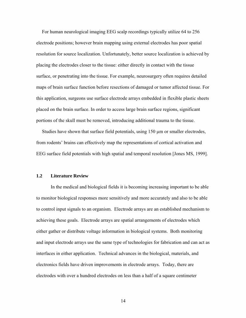
For human neurological imaging EEG scalp recordings typically utilize 64 to 256
electrode positions; however brain mapping using external electrodes has poor spatial
resolution for source localization. Unfortunately, better source localization is achieved by
placing the electrodes closer to the tissue: either directly in contact with the tissue
surface, or penetrating into the tissue. For example, neurosurgery often requires detailed
maps of brain surface function before resections of damaged or tumor affected tissue. For
this application, surgeons use surface electrode arrays embedded in flexible plastic sheets
placed on the brain surface. In order to access large brain surface regions, significant
portions of the skull must be removed, introducing additional trauma to the tissue.
Studies have shown that surface field potentials, using 150 µm or smaller electrodes,
from rodents’ brains can effectively map the representations of cortical activation and
EEG surface field potentials with high spatial and temporal resolution [Jones MS, 1999].
1.2 Literature Review
In the medical and biological fields it is becoming increasing important to be able
to monitor biological responses more sensitively and more accurately and also to be able
to control input signals to an organism. Electrode arrays are an established mechanism to
achieving these goals. Electrode arrays are spatial arrangements of electrodes which
either gather or distribute voltage information in biological systems. Both monitoring
and input electrode arrays use the same type of technologies for fabrication and can act as
interfaces in either application. Technical advances in the biological, materials, and
electronics fields have driven improvements in electrode arrays. Today, there are
electrodes with over a hundred electrodes on less than a half of a square centimeter

15
[Gonzalez C, 1997]. A present goal of electrode array development is to provide arrays
which can map a whole surface of the brain with fine grids, so that higher resolution of
voltage variations and more selective inputs can be attained.
1.2.1 Electrode Array Introduction
The two basic types of applications of electrode arrays are transmitting
information and receiving information. A recent focus of electrode arrays development
has been transmitting information as prosthesis for retinal damage. The types of electrode
arrays recently developed that receive information are primarily used to investigate
cardiac, neural, and gastric physiology responses. The most notable and intensely
researched arrays are those associated with neural electrode arrays. There are differences
between most neural and cortical electrode arrays. Neural electrode arrays are commonly
penetrating electrode arrays as well as surface electrode arrays, while cortical electrode
arrays only contact the surface.
Several performance criteria are applied when judging the effectiveness of
electrode arrays; such as: density of electrodes, electrode resistance, flexibility,
durability, compatibility with living organisms, and ability to be fabricated. Density of
electrodes defines the ability of an array to spatially resolve the variation of the signals
over an organ and provide inputs over the surface of an organ more precisely. Electrode
impedance limits the ability to resolve the relatively weak voltages that are sometimes
found in these devices and organisms. Flexibility minimizes trauma to organs during
insertion and allows better contact with surfaces during measurement. Such trauma can
interfere with the intended experimental plans and reduce the value of the data.
Durability of the electrode array is important so the operating lifetime of the device does
16
not restrict the data accumulation. Compatibility of the array with the living organisms
also assures that the array does not limit the experimental plans of the research. Ease of
fabrication is an important concern, because as arrays become smaller and higher density,
fabrication techniques are challenged to meet the dimensional tolerances and smaller
processing requirements.
Retinal degeneration affects one in four Americans that are over the age of 64
[Hung A, 2002]. In some cases, the degeneration of the photoreceptors in the retina can
result in complete blindness. Studies on retinal prostheses have shown that inducing an
electrical simulation of the remaining neural cells in the retina can produce an image for
the patient [Hung A, 2002; Sachs H, 2004]. Video cameras were linked with a
processing unit to send signals to the electrode array located on the photoreceptors. This
configuration provided the patient a pixilated image of the surroundings which was
proposed to even permit them to navigate in the future. It is important to note that the
resolution of the image is dictated by the number of electrodes that are in the
photoreceptor area.
Neural electrode arrays are the dominant driving force in the receiving type
applications of electrode arrays today. Researchers gain insight on the processing and
distinguishing information within the brain by using electrode arrays in or on top of the
brain tissue. Depending on experiment objectives, an animal’s surrounding is altered
while the responsive area of interest in the brain can be probed for voltage responses with
an attempt to correlate these responses with the initial environmental inputs.
The fundamental components of an electrode array include a substrate which
provide electrical isolation and metallic leads which carry the voltage input or output

17
signals. One issue receiving increased attention is animal compatibility with electrode
arrays. To access the brain or the retina researchers must surgically place the array in the
subject. Trauma to the animal must be minimized to maintain its health and maximize
the time of the implant test duration. In many cases the electrode array has been a
relatively bulky contraption and requires the removal of a major part of the skull or the
region behind the photoreceptors [Grumet A, 2000; Rouche P, 1998]. In the case of
flexible electrode arrays, a slot is required near the perimeter of the area of interest, so
that the electrode array can be inserted in between the skull and the dura or brain surface.
The more basic types of electrode arrays are based upon wire electrodes that
penetrate into the tissue [Tsai M, 2003; Rennaker R, 2005] in contrast to surface potential
recording electrode arrays [Franowicz M, 1995; Barth D, 1990], where conventional
machining techniques are used to form the contact sites. There are also stiff penetrating
electrode arrays [Rousche P, 1998; Normann R, 2003; Petersen R, 2000] working on the
same principle as the wire electrode arrays. Rigid electrode arrays [Grumet A, 2000] and
flexible electrode arrays are becoming more practical for implantation, but require
advanced technologies used in MEMS and Integrated Circuits. The two basic types of
flexible electrodes arrays are penetrating [Takeuchi S, 2003; Rousche P, 2001] and
surface electrode arrays [Gonzalez C, 1997; Sachs H, 2004; Nakauchi K, 2005; Sandison
M, 2002]. Both types of arrays are designed to conform to the surface of the biological
area and still maintain the ability to adjust to the small movements resulting from the
animal’s locomotion. Penetrating flexible electrode arrays are made to sense the different
brain activity at different depths into the brain. Surface flexible electrode arrays are
made to activate the surface of the retinal photoreceptor or record neural surface

18
potentials. Flexible electrode arrays attempt to be flexible, smooth, thin and light in order
to prevent causing mechanical damage to the retina or the brain surface. At the same
time, the electrodes need to be robust to insure function over time. Most flexible
electrode arrays are made of a polyimide material; due to its biological compatibility and
its ability to be manipulated.
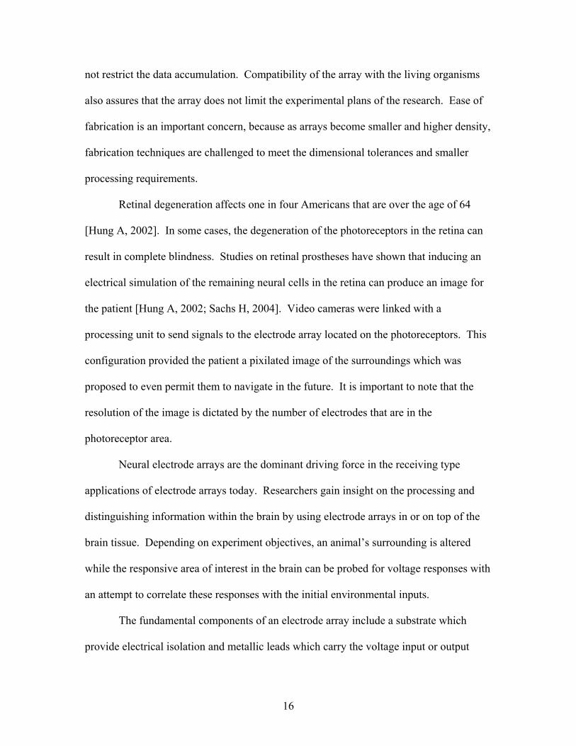
1.2.2 Wire Electrode Arrays
A pin microwire electrode array fabrication process is described by Tsai for the
purpose of conducting neural recordings on monkeys and rats [Tsai M, 2003]. He
described a simple construction of 8 to 96 Teflon insulated microwires with inter-
electrode separation of 400 to 500 µm as shown in Figure 1.2. The wires were laid flat in
rows, where epoxy bonded them together. This configuration seemed to be a crude and
rudimentary way to accomplish the goals, but served the purpose to gather neural
recordings below the surface of the brain.
Figure 1.2: Microwire electrode array used by Tsai [Tsai M, 2003].
Rennaker from University of Oklahoma manufactured electrode arrays in a
manner similar to Tsia [Tsai M, 2003]. Rennaker described the fabrication of a 10 by 10
electrode array made of polyimide insulated tungsten wires with a 125 µm diameter and
19
250 µm spacing [Rennaker R, 2005]. The wires were fed through a conventionally
drilled alignment jig to evenly space the wires.
It is thought by some that the surface potential recording electrode arrays are just
as effective as a penetrating electrode arrays. For example, Barth from the University of
Colorado manufactured an electrode that was an 8 by 8 electrode array [Barth D, 1990]
similar in design and construction to Rennaker [Rennaker R, 2005]. The main difference
was that the substrate and wires were flush with each other and the information gathered
from the electrode array was from the surface, instead of below the surface of the brain.
The density of electrodes using these approaches to manufacturing electrode
arrays is limited by their dependence on conventional machining. These approaches
usually cost less than ten dollars and paired with their ease of fabrication make them very
appealing for simple cortical recordings.
1.2.3 Stiff Penetrating Electrode Arrays
Rousche from University of Manchester Institute of Science and Technology used
a different type of electrode array, called the Utah Intracortical Electrode Array, to
implant into cats [Rousche P, 1998]. It was a 10 by 10 array of penetrating silicon
microelectrodes, measuring 1.5 mm in length. Unlike previous electrodes the Utah
Intracortical Electrode Array takes voltages underneath the surface of the cerebral cortex,
i.e., the surface of the brain. To fabricate the electrodes a monolithic piece of silicon was
micro-machined and acid-etched to form the basic substrate of the electrode array. The
first 100 µm of each tip was built up by layers of Pt, Ti, W and another layer of Pt which
was deposited to covert the needles into electrodes. Each of the needle electrodes was
20
insulated from its neighbor by a glass dielectric. The electrode arrays possessed an
average initial impedance of 156 ± 32 kΩ at 1 kHz.
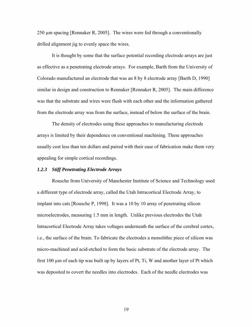
1.2.4 Rigid Electrode Arrays
Grumet from Massachusetts Institute of Technology used a series of patterned
conductive and insulating layer on a rigid glass substrate to stimulate and record retinal
information [Grumet A, 2000]. The rigid electrode array is shown in Figure 1.3. The
fabrication of the electrode array included a number of sputtering, spin coating,
patterning and etching steps. Gold and platinum black are used as the conductive layers.
The platinum black provided a conducting base that was electrolytically coated with gold
to reduce the impedances at 1 kHz to 100 kΩ.
Figure 1.3: Rigid electrode array made from a rigid glass substrate [Grumet A, 2000].
Polyimide and silicon nitride were used for the electrical insulation. For this
MEMS technology was utilized to create a tightly packed electrodes, however the array’s
flexibility was limited by its stiff substrate.
21
1.2.5 Flexible Penetrating Electrode Arrays
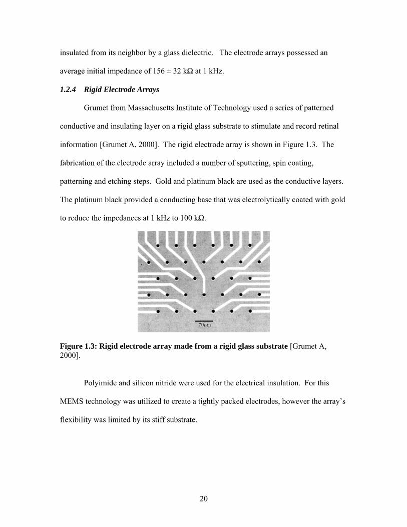
Takeuchi at the University of Tokyo developed a flexible electrode array that
penetrated into the surface of the brain utilizing MEMS technology [Takeuchi S, 2003].
The electrode array was fabricated by electroplating nickel onto a silicon wafer, spin-
coating with a polyimide insulator, and then depositing an aluminum/titanium layer with
a vacuum evaporator. The aluminum was patterned and etched using a wet etch then
encapsulated by another layer of polyimide. The polyimide was then patterned by
masking it with aluminum and introducing it to an oxygen plasma to expose multiple
electrodes. The silicon was then removed from the set up using a deep reactive ion etcher
and a XeF2 etching process. The polyimide substrate was then cut, and the probes were
folded up making penetrating probes. A schematic representation of the resulting
electrode array is shown in Figure 1.4. This electrode array was flexible and allowed
recording of information in different locations and depths of the brain. Rousche made a
very similar electrode array prior to the Takeuchi electrode array [Rousche P, 2001] using
a similar process.
Figure 1.4. Flexible recording electrode array used for recording evoked responses by penetration of the brain [Takeuchi S, 2003].

22
1.2.6 Flexible Surface Electrode Arrays
Sandison, at the University of Glasgow, in the UK, made use of a polyimide
based flexible electrode array for neural recordings [Sandison M, 2002]. The electrode
array was fabricated by sputtering gold onto a polyimide film and patterning it using
photolithography and wet etching. The gold was then insulated by coating it with a liquid
polyimide and by a spin coating process. After being baked the liquid became solid,
encapsulating gold circuitry. The thicknesses of these electrodes typically range from
100 µm to 200 µm [Nakauchi K, 2005; Sandison M, 2002] thick. Successful recordings
have been taken from flexible electrode array implants for longer than 3 months [Sachs
H, 2005], impedance values ranging from 10 kΩ to over 1 MΩ [Nakauchi K, 2005].
Sachs’s electrode array is similar to the electrode array this thesis is on, but does not
possess the qualities to be inserted underneath the skull of a rat. Gonzalez at the
University of Madrid has fabricated and tested flexible arrays consisting of up to a
hundred electrodes used for nerve and muscle tissue recordings [Gonzalez C, 1997].
Gonzalez used photolithography to construct his array. A retinal flexible electrode array
is shown below in Figure 1.5 [Sachs H, 2005], where an arrow highlights one of the 20
electrodes. The electrode array was implanted in cats with damaged retina between the
pigment epithelium layer and the outer layer of the retina to stimulate intact retinal cells.

23
Figure 1.5: Flexible electrode array used for penetrating retinal recordings [Sachs H, 2005].
1.2.7 Whisker Actuators
One of the most frequently used stimulation that researchers use when recording
cortical responses on rats is actuating the anim
Renal’s whiskers. This is accomplished by moving the whisker quick enough and
far enough so that the rat’s response can be recorded using electrode arrays. To do this
many have developed their own whisker actuating devices involving piezoelectrics
[Harris J, 1999; Mirabella G, 2001; Rousche PJ, 1999; Kublik E, 2001], solenoids[DM
Rector, 2005], devices creating puffs of air [Sachdev R, 2003] and subcutaneous implants
[Devilbiss DM, 2002]. Each of the devices has different dampening coefficients that
affect the rat’s response. The closer an actuator deflection could be to a square wave
deflection, the less the rat will be affected by the actuator’s reverberations. Whiskers are
chosen to be actuated one at a time, rows at a time, groups at a time and different
combinations of time staggered actuations on different whiskers.
Piezoelectric actuators are the most commonly noted whisker actuation devices in
use. The two types of piezoelectric whisker actuators mentioned most frequently in the

24
literature are bimorphs (a two layered piezoelectric cantilever) and piezoelectric wafers.
Both types of actuators’ displacements were reported to be between 80 μm and 100 μm
[Harris J, 1999; Mirabella G, 2001; Rousche PJ, 1999; Kublik E, 2001]. Piezoelectrics
have good response times, but have limited travel unless large voltages are applied.
Solenoids are a cheap and effective way for actuating whisker. Solenoids have
the ability for large deflections, but are capable of producing low deflections as well.
Solenoid deflections have been used for whisker deflection such as 75 μm [Rector DM,
2005] as well as controlling rise speeds of 1 mm in 1 millisecond [Krupa DJ, 2000]. The
electromagnetic device has low dampening, creating a large ring out time.
Air puffs have also been used to actuate whiskers. A triggered solenoid releases
air from a pressurized air line to let the blast of air stimulate the whiskers. The time the
air takes to reach the rats face is calculated and subtracted from the total time before the
evoked response. This gives a more accurate measurement of evoked response time for
an air puff [Sachdev R, 2003]. While air puffs allow a free moving animal and permit the
whiskers to be in a natural arrangement, the resolution of air puffs does not have the
accuracy needed for many whisker stimulation experiments.
While physical movement used in the methods above can elicit well controlled
whisker movements, they are difficult to actuate on a freely moving animal. For an
awake animal a method has been developed to activate the pathway by electrically
stimulating the infraorbital nerve via the nerve cuff. These procedures lack the ability to
be spatially selective when intending to stimulate certain areas. This situation was
improved when a procedure was developed that implants an indwelling subcutaneous
electrode that delivers repetitive focal electrical stimulation to the whisker pad.

25
Recording can then take place on freely moving rats over a period of days to weeks
[DM. Devilbiss, 2002].
The piezoelectric and solenoid actuators listed above are the portion of the whisker
actuators that supply the movement. The other necessary component to stimulate
whiskers is the connection between the actuator and the whisker. Attachment methods
used for this purpose are stainless steel wire wrapped into a loop [Krupa DJ, 2000], a
lever arm [Rousche PJ, 1998] hypodermic tubing [Rector DM, 2005], a thin needle
attaching with glue [Kublik E, 2001], Mesh screen [Shen H, 2002] and wire hooks
[Mirabella G, 2001; Rousche PJ, 1999], all of which the whisker could be set on or in to
make a physical connection.
1.3 Research Objectives
Although a number of electrode arrays have been developed for both acute and
chronic/awake preparations in animals [Rousche P, 1999; Kipke V, 1999]; these
electrodes are either penetrating unit electrodes, or require large portions of the skull to
be removed in order to expose enough of the brain surface for mapping [Jones MD,
1999]. Large skull openings are difficult to maintain chronically (long periods of time:
weeks, months) in small rodents and stainless steel EEG screws are problematic in thin
bone. In either case, it is difficult to maintain such chronic preparations for extended time
periods which enhance the amount of data which can be obtained from a single animal.
Obviously an improved electrode array is needed in order to advance this field of
biological investigation.

26
Several laboratories have developed electrode arrays using flexible substrates,
[Kipke V, 1999; Takeuchi, 2004; Grumet, 2000] primarily for insertion into cortical
tissue to minimize the trauma associated with placing rigid objects into tissue. These
approaches utilize polyimide compounds as flexible substrates, but are not capable of
recording from tissue surfaces.
The main objective of this thesis work was to develop a device which could record
from a large surface of cortical tissue with minimal trauma for long term recordings with
a electrode density of greater than 200 electrodes per square centimeter, electrode
impedance values not exceeding 1 MΩ, durability to withstand implantation, biological
compatibility with animal, ability to be fabricated in high quantities, and thin enough to
be slipped between the dura and the skull yet stiff enough to be capable of insertion.
A 64 channel flexible electrode array, which was thin enough to be inserted between the
rat’s skull and dura and be placed on the surface of the cortex was to be designed,
fabricated and tested on rats.
Obtaining evoked response data requires a stimulation of a whisker. To do this a
whisker actuator was required. It should be fabricated so the sound it generates will not
affect the evoked response of the rat, create a deflection significant enough to create a
large evoked response, a minimized ring out time, and a quick response time. The
whisker actuator must be tested and characterized to acquire the traits of the whisker
twitch.

27
Chapter 2. DESIGN AND FABRICATION
2.1 Electrode Array Design
An electrode array must include four things: an array of conductive electrodes to
extract information from the subject, an insulating material to isolate one electrode from
another, a substrate material to construct required structures and a connection interface
for data storing and processing units. This section will describe the electrode array’s
components design, materials chosen, and fabrication techniques.
2.1.1 Electrode Array Configuration
The electrode array design was based upon a square grid of 8 by 8 electrodes,
located within a 5.4 x 5.4 mm area. This portion of the electrode array was intended to
carry cortical information from the implantation site. The arrangement satisfied the
required electrode resolution. The electrodes were chosen to be 150 μm circles evenly
spaced over the area. Connected to the electrodes were 50 μm leads to act as a
connection between the electrodes and the connector pads. The connector pads were 150
μm wide lines, where electrical connection could occur. Between every adjacent
connector pad was a 150 μm gap. The total height of this portion of the electrode array
was 22.25 mm. The resultant design consisted of a circuit of 64 separate coupled leads,
electrodes and connector pads shown in Figure 2.1.A. An enlargement of the electrode
portion of the electrode array is shown in Figure 2.1.B

28
A. B.
Figure 2.1: Electrode array gold circuit pattern: A) complete electrode array with aligning targets B) Close up of electrode portion of the electrode array.
To isolate leads for each one of the electrodes a material was required to
encapsulate the electrode array. The only areas exposed were the round electrodes at the
bottom of Figure 2.1.B and the connector pads at the top of Figure 2.1.A. The electrodes
were left exposed so the electrodes can come into contact with the saline within the rat’s
skull. The connector pads were left exposed to enable connection with this portion of the
device.
A thin, flexible material was necessary for the substrate to make certain that the
electrode array was implantable into the rat’s skull without too much trauma. A stiff
electrode array would often puncture the dura and brain. A thick electrode array would
increase the size of the slot required for implantation.
To connect the processing computer to the electrode array a connection scheme
was needed. The interface already in place for the host computer was a pin connector.
The connection must link the pin connector to the gold connection pads.

29
2.1.2 Material Selection
The final electrode array materials chosen were a Kapton substrate, a patterned
gold patterned electrical circuit, and an SU-8 electrical insulating layer. A circuit board
and Zebra connector were used to make the electrical connection from the gold circuit to
the pin connectors.
A polyamide, Kapton film (Dupont, Wilmington DE) was chosen as the substrate
due to its mechanical properties, flexibility, retention of mechanical and electrical
properties over a wide temperature range with excellent chemical resistance, and history
in flexible printed circuits. Some relevant material properties of Kapton are listed in
Table 2.1. [Kapton, 2005]
Ultimate Tensile Strength 231 MPa Yield Point 69 MPa
Tensile modulus 2.5 GPa Dielectric strength 303 kV/mm
Maximum Operating Temperature 400 ºC Table 2.1: Material Properties of Kapton [Kapton, 2005].
It was necessary for the substrate to have a high maximum operating temperature
and chemical resistance to prevent damage during future fabrication steps. A curing step
for the SU-8 requires a hotplate bake at 200 ºC. There are numerous chemicals that were
necessary for many of the processes, making chemical resistance imperative.
The Kapton thickness was chosen to be 25 µm. The decision making process was
governed by the competing requirements that the array was stiff enough to retain form so
that it could be inserted into the rats skull, yet still flexible so that it did not cut into the
dura.

30
Gold was the material that was chosen to make the circuit of 64 electrodes, leads,
and connections pads in Figure 2.1. Previous success of others [McKenney DJ, 2005]
along with first hand knowledge of depositing gold on Kapton made gold a reliable
choice. The ability of gold to be patterned using lithographic techniques also made it an
appealing selection. A 300 nm layer was selected for the gold’s thickness because of
experience in adhesion using DC Sputtering at that thickness. If the gold layer is
deposited much thicker than 300 nm the adhesion was found to be poor and if deposited
much thinner than 300 nm the gold was found to flake off.
Titanium-Tungsten alloy was select for an adhesion layer between the Kapton and
the gold layer, because of its proven success through first hand knowledge. A 5 nm
thickness was preferred because of its regular success for adhesion.
SU-8 2010(MicroChem, Newton, MA), an epoxy-based negative photoresist, was
chosen for its insulating properties, thermal stability, good chemical resistance and its
ability to be patterned using standard photolithographic techniques. SU-8 thickness can
be altered by varying the spin coating speed and the solvent ratio to get thicknesses
between 1 and 300 μm [SU-8, 2005]. A thickness of around 13 μm was chosen because
it gave the correct overall stiffness for the Kapton, Titanium-Tungsten, gold, SU-8
composite when physically tested by implanting it into a rat.
A circuit board was constructed to be one of the components that connected the
pin connector and the gold connection pads. The pin connector was the component of the
electrode array that interfaces with the host computer. The circuit board was designed to
have 64 exposed connection pads matching the connection pads of the gold on one end.

31
The other end of the circuit board was comprised of 64 holes where the pins from the pin
connector were to be inserted.
To make connection between the constructed circuit and the gold connection pads
a Carbon Zebra Elastomeric Connector, Series 2005 (Fujipoly, Tokyo, Japan), was
chosen. The Zebra connector consisted of layers of conductive material and
nonconductive elastomeric material alternating at a pitch of 50 µm [Zebra, 2005]. The
zebra connector was sandwiched between the circuit board and the electrode array.
Figure 2.2 shows a graphic of the zebra connector concept.
Figure 2.2: Zebra connector making electrical connection between the circuit board and the gold connector pads of the electrode array

32
Figure 2.2 shows that the circuit board and the electrode array do not have to be
perfectly aligned to make an electrical connection. Since the pitch of zebra connector is
50 μm and the pitch of both the circuit board and electrode array is the minimum
suggested thickness, 150 μm [Zebra, 2005], the alignment could be as much as 100 μm
off and the electrode array could still be effective. The dimensions of the zebra strip
were 2.5 mm high to make room for the proper amount of compression, 1.5 mm wide to
make acceptable contact with the gold connector pads, and 25 mm long to have the length
to get the entire 64 electrode array row of connection pads. The Zebra connector required
a significant compression to maintain acceptable contact with the surface between the
gold connection pads and the circuit board connection pads. Successful electrodes had a
Zebra connecter compression distance measured to be 0.5 mm, or twenty percent of the
overall height.
To fulfill the need for applied squish on the zebra connector for electrical
connections a jig was design to provide the proper compression. The design involved
two bolts, one on each end, so that when they were tightened, the two plates would move
together to clamp down on the different portions of the electrode array. It was also
designed to have an alignment pin that aligned the circuit board to the Kapton composite.
This jig was labeled an alignment clamping jig.
2.2 Electrode Array Fabrication
Electrode array fabrication can be divided into microfabrication and
macrofabrication. The microfabrication portion of making the electrode array is done in
a cleanroom environment emphasizing precision and cleanliness. The Kapton substrate,

33
the patterned electrical gold circuit, and the SU-8 electrical insulating layer are under the
microfabrication label. The macrofabrication portion of the electrode array construction
involves conventional machining and interfacing with macroscopic equipment.
Appendix A and Appendix B.1 through B.11 describes both the microfabrication and
macrofabrication instructions of the electrode array in detail.
2.1.1 Microfabrication Processes
The procedures in this process were carried out in a class 1000 clean room to
maintain cleanliness, promote adhesion between layers and reduce surface contamination.
Using Kapton tape, a 25 μm thick Kapton substrate was attached to a glass slide to
provide a rigid structure to endure the fabrication processes, described in Appendix B.2.
In previous prototype electrode arrays a 50 μm thick Kapton substrate was used. The
thicker substrate was not flexible enough to go through the implantation phase, where the
electrode array was inserted between the skull and the dura, without damaging the dura.
The 25 μm substrate was prepared by an acetone, isopropanol, deionized water wash and
a RF plasma etch (PE-2000 Plasma Etching system, South Bay Technology INC, San
Clemente, CA) at 100 Watts for 3 minutes. Procedures for plasma etching are explained
in Appendix B.3. A DC Magnetron system (Edwards Auto 306, Wilmington, MA) was
used to sputter a 5 nm layer of a titanium-tungsten alloy onto the Kapton substrate by
subjecting 100 Watts for 51 seconds, followed by a 300 nm gold layer by applying 75
Watts for 23 minutes and 12 seconds. Both gold and titanium-tungsten layers were
sputtered in the presence of Argon gas at 7.5x10⁻³ torr. Prior to the Argon gas addition
the sputtering chamber was pumped down to 9x10⁻⁷ torr. The titanium-tungsten alloy
layer was used as an intermediary layer between the Kapton film and gold to promote

34
adhesion. The sample was then plasma etched again using the same conditions as the
first plasma etch.
Photolithography was used to pattern the gold to produce the circuit. A thin layer
of Hexamethyldisilazane (Fluka, Switzerland) was applied first by spin coating it a 3000
rpm for 30 seconds, followed by spin coating a layer of AZ5214-EIR (Clariant,
Somerville, NJ) photoresist on the Kapton substrate at 3000 rpm for 30 seconds. The
slide was then placed on a hotplate and baked for 2 minutes at 110 ºC. The
Hexamethyldisilazane was used as an adhesion promoter layer between the photoresist
and the gold. The patterning of the photoresist was performed by flooding the photoresist
with ultraviolet light for 27 seconds through a mask which changes the chemistry of the
photoresist making it soluble for etching. The unwanted photoresist was removed by
submerging the slide into a bath of AZ-400K Developer (Clariant Somerville, NJ) for 60
seconds. The unwanted gold was removed by submersion into a gold etch bath (Gold
Etch-Type TFA, Transene Company, Danvers, MA) for 90 seconds ± 45 seconds. The
gold etchant was used several times before disposal, so this affected the concentration of
the reacting chemicals and caused large differences in etching time. The titanium-
tungsten alloy was removed by submersion into a hydrogen peroxide bath for 45 seconds
in the same pattern as the gold. An acetone wash was used to remove the photoresist
leaving behind the completed gold circuit shown in Figure 2.1. As shown in the figure
there are gold targets on both sides of the electrode for alignment. Finally the slide was
baked on the hotplate for 3 minutes at 120 ºC.
Photolithography was also used to pattern the SU-8, the electrical insulating layer.
To prepare the Kapton and gold sample for SU-8 the sample was plasma etched for 3

35
minutes at 100 Watts, washed with acetone, isopropanol, and deionized water, then baked
to remove all remaining organics at 200 ºC for 8 minutes. A single layer of 2010 SU-8
photoresist was spun on top of the Kapton and gold circuit, using a spincoater at 2000
rpm for 30 seconds, then baked to crosslink the SU-8 fibers at 65 ºC for 2 minutes
followed directly by a 95 ºC for 3 minutes on a different hotplate. A mask was used to
expose everything with UV light except the gold connection pads, at the top, and the
smaller gold electrodes, at the bottom. The sample was again baked at 65 ºC for 3
minutes followed directly by a 95 ºC for 5 minutes on a different hotplate. The unwanted
SU-8 was removed using SU-8 developer bath (MicroChem, Newton, MA) for 3 minutes
with strong agitation. The sample was finally washed with acetone, isopropanol, and
deionized water, dried, and baked again at 200 ºC for 8 minutes to insure the thermal
properties of the SU-8. The resultant SU-8 thickness was approximately 13 μm. A
schematic representation of the clean room fabrication process is shown in Figure 2.3.

36
Figure 2.3: Representation of microfabrication steps in making the electrode array: A) Prepare Kapton substrate B) Sputter on Au and TiW C) Pattern Au and TiW D) Spin on SU-8 insulating layer E) Pattern SU-8.

37
2.1.2 Macrofabrication Processes
Once the cleanroom fabrication of the electrode array was finished, an electrical
connection between the electrode array and the test equipment was achieved. To
accomplish this connection, a corresponding circuit board was constructed that was
matched up with the exposed, gold connection pads. Electrical connection between the
electrode array and a corresponding circuit board was obtained by using a Carbon Zebra
Elastomeric Connector.
The Kapton of the electrode array and the circuit board both have holes in them
that were fitted firmly around alignment pins on a clamping jig ensuring that the fine
lines of the electrode array and the circuit board match up correctly. The whole assembly
was then clamped together using the alignment clamping jig. The finished fabricated
electrode array is discussed and shown in Section 4.1
Previous electrode array prototypes involved using conductive epoxy to make the
electrical connection between the gold pads of the electrode array and the pin connector
instead of the zebra connector and the circuit board. Holes were drilled into the Kapton
film around the area of the gold connector pad for the pin connector to go through. The
electrical connection was then made with conductive epoxy from the gold pad to the
connector. These attempts were unsuccessful mainly due to the failure of the adhesion of
the gold through the drilling process. Some gold would lose contact with the substrate
making it impossible to make electrical connection.

38
2.2 Whisker Actuator Fabrication
As discussed in the introduction section, cortex electrode arrays are often used to
measure the response from whisker deflection. In this investigation three different types
of whisker actuator have been constructed and used in order to evaluate the performance
of the flexible electrode array.
The actuators must be able to generate enough force to deflect the whisker. To
statically deflect a whisker 1x10-13 Newtons of force must be applied, using the standard
beam Equation:
3
3LEIF δ
= [Equation 2.1]
In Equation 2.1 the whisker was assumed to be fixed at one end. L is the length of the
whisker (2 cm). δ is the deflection of the whisker (50 μm). E is the elastic modulus of
the whisker (2.75 GPa [Herzog B, 2005]). I is the moment of inertial for an 80 μm
diameter rat whisker.
These three types of actuators are made from a speaker, a piezoelectric bender,
and a piezoelectric stack actuator. The goal of each whisker actuator was to be able to
deflect a whisker over 50 μm and have a consistent deflection. For all three cases a piece
of hypodermic tubing was the method of connection for the rat whisker.
2.2.1 Speaker Whisker Actuator
The speaker whisker actuator, shown in Figure 2.4, was the cheapest and simplest
to activate of the actuators. It is made from an 8 Ohm speaker attached to a 10 centimeter
section of hypodermic tubing with 5 minute epoxy. The speaker is a solenoid that
linearly moves up and down. The hypodermic tubing is a cantilever that moves the

39
whisker in a vertical direction as the solenoid goes up and down. To statically deflect
added mass of the epoxy and the hypodermic tubing the speaker must subject a 0.01
Newton force using Newton’s second law.
Figure 2.4: Speaker whisker actuator composed of an 8 ohm speaker and hypodermic tubing.
2.2.2 Piezoelectric Bender Whisker Actuator
The piezoelectric bender (bimorph) whisker actuator was composed of a half inch
length of hypodermic tubing, a piezoelectric bimorph cantilever (American Piezo), and
an acrylic clamping and mounting attachment. The hypodermic tubing was attached to
the end of the cantilever, where there is the maximum deflection, using a small amount
super glue followed by 5 minute epoxy. The area at the end of the cantilever, where the
hypodermic tubing was attached was minimized because the epoxy restricts that portion
of the piezoelectric bender from bending, and hence reduces deflection. Piezoelectric
bimorphs require large actuation voltages. The bender used here can deflect over 1.5 mm
at 150 V. The piezoelectric bender can subject 0.0004 Newtons of force for every Volt

40
applied to it almost linearly up to 150 V [American Piezo, 2005]. The piezoelectric
bender was secured by mounting and tightening it in an acrylic clamp. Figure 2.5 is a
photograph of the finished piezoelectric bender whisker actuator.
Figure 2.5: Piezoelectric bender whisker actuator composed of acrylic holder, piezoelectric bender and hypodermic tubing.
2.2.3 Piezoelectric Stack Whisker Actuator
A piezoelectric stack is a portion of piezoelectric material made for fast reaction
times, large deflections and consistent deflections. It deflects in one direction and, like
the piezoelectric bender, requires large voltages for significant deflections. The
piezoelectric stack used produced deflections greater than 30 μm with 120 volts. To
achieve these voltages a LVPZT(Low Voltage PZT) amplifier was used to amplify a 12
Volt signal from a function generator, to 120 Volts.
The piezoelectric stack whisker actuator was modified with a lever arm so that
different amplitudes could be achieved using the same output signal. A 15 cm long 3.2
mm diameter steel rod was attached to the stack with a pivoting connection as shown in

41
Figure 2.6. To amplify the defection coming out of the stack another pivoting point was
made that could be varied along the length of the rod. This created an amplifying lever
arm that was used to increase the stack deflection at the end of the hypodermic tubing to
an amplification ratio of 1 to 15.5.
Figure 2.6: Piezoelectric stack whisker actuator, which magnified the piezoelectric stack actuators movement.
2.3 Whisker Actuator Deflection Test Setup
To test the consistency, the ring out and the magnitude of the deflection of each of
the whisker actuators a laser vibrometer was used. Laser vibrometers are devices that are
capable of finding the deflection, the velocity, and acceleration of objects without
touching them. A Polytec OFV-5000 Vibrometer Controller with an OFV 511 Fiber
Interferometer and a VD-06 velocity output decoder was used. This Laser vibrometer

42
uses a helium-neon laser as the light source. When the laser is reflected off of the
vibrating surfaces the frequency is changed due to the Doppler Effect. The change in
frequency is then measured by the decoder to output a displacement, velocity or
acceleration of the whisker actuator. This data can be routed to an oscilloscope or a host
computer. Figure 2.7 shows the test setup for deflection the whisker actuators.
Figure 2.7: Deflection setup for whisker actuators where the laser vibrometer would detect the vibrating actuator.
To deflect the actuators a Tektronix AFG310 arbitrary function generator was
used to send a single pulse into each of the actuators. The input pulse was primarily a 0.2
ms square wave.
2.4 Electrode Array Impedance Test Configuration
Each electrode array that was fabricated went through initial quality and
performance tests prior to being considered for use on animal subjects. This quality

43
testing was aimed at evaluating the overall electrical impedance, potential open circuits
and areas of high resistances on subcomponents such as the pin connectors, the circuit
board, zebra connector, electrode array, and even into the saline solution. Figure 2.8
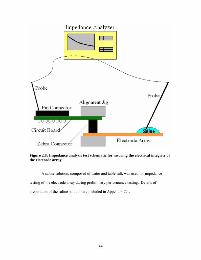
illustrates the electrode array impedance test configuration. An Agilent 4294A precision
impedance analyzer was used at 1kHz to test the impedance of the electrodes. It had a
measurement range of 40 Hz to 110 MHz. A small puddle of saline was placed over only
the exposed gold electrodes through the SU-8, using a pipette. One of the impedance
analyzer’s probes was submerged into the saline solution and fixed. The other probe was
connected to the appropriate conductive contact surface on the pin connector for each of
the 64 electrodes.
44
Figure 2.8: Impedance analysis test schematic for insuring the electrical integrity of the electrode array.
A saline solution, composed of water and table salt, was used for impedance
testing of the electrode array during preliminary performance testing. Details of
preparation of the saline solution are included in Appendix C.1.

45
2.5 Animal Testing
2.5.1 Animal Testing Equipment
For animal tests there were three different types of equipment. The first type of
equipment was devices that assisted in the stimulating of the rat whisker. The second
type of equipment used was devices that assisted in the recording of the response to that
stimulated whisker. The last type of equipment was used to hold the rat’s environment in
a consistent state, where a consistent body temperature was maintained and movement
was minimized.
The stimulating equipment consisted of a host computer, stimulator and a whisker
actuator. The host computer would send a pulse input into the stimulator, which would
send an amplified pulse to the whisker actuator.
The recording equipment consists of the electrode array, the amplifiers, an A/D
converter and the host computer. The electrode array that was constructed was the device
that is the interfaced between the rat and data processing units. The amplifiers take the
evoked response signal and amplify the amplitude of it. The A/D converter takes an
analog input and converts the signal into a digital output. Then the host computer
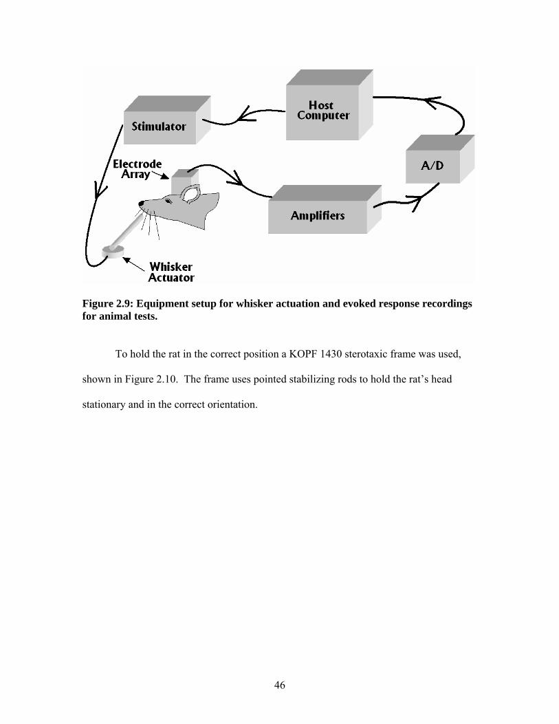
receives and stores all of the digital information for each of the 64 electrodes. Figure 2.9
is a schematic of the organization of the animal testing equipment.
46
Figure 2.9: Equipment setup for whisker actuation and evoked response recordings for animal tests.
To hold the rat in the correct position a KOPF 1430 sterotaxic frame was used,
shown in Figure 2.10. The frame uses pointed stabilizing rods to hold the rat’s head
stationary and in the correct orientation.

47
Figure 2.10: Sterotaxic frame used for rat stabilizing.
When needed, a clamp was used over the upper jaw to guarantee stability. To
regulate the subjects body temperature an Isotemp 3016 water heater was used. It uses
heated water pumped below the subject to maintain the desired body temperature.
2.5.2 Animal Testing Methods
To test the electrode array standard cranial surgical methods were used. Male
Sprague-Dawley rats (300-400 g) were implanted with an electrode array for testing. All
procedures were approved by The Animals Care and Use Committee at Washington State
University. The animals were anesthetized with Ketamine/Xylazine cocktail (100mg/kg
and 10 mg/kg respectively) and body temperature maintained at 37ºC. Twenty percent of
the initial dose was administered as supplemental anesthesia when needed.

48
The animals were then placed in the sterotaxic frame and a 6mm by 1 mm slit was
drilled in the rostro-caudal direction between bregma and lambda, just lateral to the
midline placement of the electrode array as can be seen in Figure 2.11. The midline edge
of the craniotomy was beveled to assist in the insertion of the probe. Using a firm plastic
knife inserted under the bone, the dura was separated from the skull to promote an easy
electrode array insertion. The electrode array was then slipped between the dura and the
skull over the whisker barrels somatosensory cortex on right side of the animal.
Figure 2.11: Electrode placement just lateral of the midline and caudal of the bregma.

49
Figure 2.12 shows the comparison of the size of the electrode array to the size of
the whisker barrels approximately. The electrodes have an interelectrode distance of 750
μm. The electrode array was made large enough to cover all of the primary whisker
barrels.
Figure 2.12: Electrode spacing in reference to the whisker barrels: A) Electrode size and spacing for electrode array B) Whisker barrel micrograph [Kyriazi H, 2005].
The host computer sent a randomized pulse input into the stimulator, 1 to 2
seconds apart. The stimulator then sent a 5 V, 0.2 ms pulse to the 8 Ohm speaker
whisker actuator, which deflected the whisker 50 μm. The response from the rat was
gathered from the animal, by the electrode array. That signal was then amplified and ran
through A/D converter. Surface field potentials recorded by the 64 channel electrode

50
array were collected with a 16 bit digitizer at 20 kHz. Typically, 20 to 100 responses
were averaged and stored in the host computer for each whisker.

51
Chapter 3. WHISKER ACTUATOR RESULTS
The purpose of a whisker actuator’s purpose is to stimulate a whisker in order to
monitor the evoked response by using an electrode array inserted over the cortex. The
whisker actuator design required the specifications of the deflection amplitude, dynamic
charcteristicsring out length and complexity of the apparatus. A deflection between 50
μm and 150 μm has found to be a satisfactory range to get a quality evoked response
from the rats. Each of the whisker actuators discussed below are capable of generating a
whisker deflection of at least 50 μm. A ring out time is defined here as the period of time
spanning from when the actuator is initially triggered to the time when the amplitude
decreases to 5 % of the maximum amplitude. Shorter ring out times are better, since a
more direct correlation of whisker deflection and evoked response may be established. A
0.2 millisecond square input pulse was used for all experiments using this electrode array.
Like the short ring out times, short input deflection times also create a better correlation
with evoked responses. When long input times are used a response generates from the
upward motion of the twitch and the downward motion of the twitch.
To understand the evoked response of a rat, it was important to know the
characteristics of the actual movement applied to its whisker during deflection. A laser
vibrometer was used to monitor the deflection trace from the actuators as described in
section 2.3. Deflection traces were the most common measurement used for clarifying
the whisker actuator experiments. An attempt was made to reduce audio sound of the
whisker actuators since this sound has also independently been shown to generate an
evoked response.

52
The three types of whisker actuators examined in this study were the speaker
whisker actuator, the piezoelectric bender actuator and the piezoelectric stack actuator.
The analysis of these whisker actuators will now be discussed.
3.1 Speaker Whisker Actuator Analysis
Figure 3.1 shows the deflection trace of the speaker whisker actuator. The ring
out of the speaker lasted, approximately, 0.15 seconds when subjected to a 0.2 ms, 5V
square wave input pulse. The maximum initial peak to peak deflection of the speaker
was found to be approximately 75 μm.
-50
-40
-30
-20
-10
0
10
20
30
40
0 0.05 0.1 0.15 0.2 0.25 0.3 0.35 0.4
Time (seconds)
Defle
ctio
n (μ
m)
Figure 3.1: Speaker whisker actuator deflection trace.
The response time of the speaker whisker actuator system was found to be 0.35
milliseconds, shown in Figure 3.2. The response time was determined from the first
downward slope of the input pulse to the initial deflection of the speaker whisker

53
actuator. The resonant frequency during the ring out was found to be 40 Hz, using the
Fourier Transform technique. The sound of the speaker whisker actuator was a very faint
auditory tick.
-40
-35
-30
-25
-20
-15
-10
-5
0
5
10
-0.0005 -0.0003 -0.0001 0.0001 0.0003 0.0005 0.0007
Time (seconds)
Defle
ctio
n (μ
m)
input voltageDeflection in microns
Figure 3.2: Response time example of the speaker whisker actuator found to be 0.35 milliseconds.
In figure 3.3 the deflection of the speaker whisker actuator increases as higher
voltages were applied to a 0.2 ms square pulse. Three separate tests were completed to
obtain the average defection for the speaker whisker actuator at 7 different voltage inputs.
The standard deviations for each of the deflections were found to be below 6 μm. The
maximum deflection was measured to be 116 μm with approximately a 10 V input
voltage. The minimum deflection was measured to be 9 μm with a 2 V input voltage. At
a twelve volt input voltage the value does not follow the linear curve.

54
0
20
40
60
80
100
120
140
0 2 4 6 8 10 12 14
Voltage into device (V)
Def
lect
ion
(μm
)
Figure 3.3: Variation of the speaker deflections with varying applied voltages.
3.2 Piezoelectric Bender Actuator
The piezoelectric bender actuation was tested in the same manner as the speaker
whisker actuator using an applied 0.2 ms, 12 V square wave input voltage. A single ring
out is shown in Figure 3.4. The response time was found to be 0.075 ms and the ring out
time was 0.12 seconds for the piezoelectric bender. When actuated the piezoelectric
bender whisker actuator made a very faint tick sound.
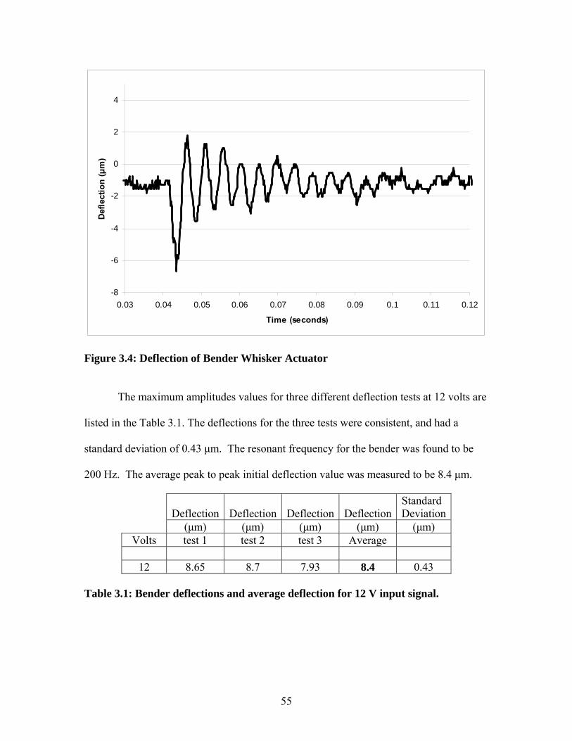
55
-8
-6
-4
-2
0
2
4
0.03 0.04 0.05 0.06 0.07 0.08 0.09 0.1 0.11 0.12
Time (seconds)
Def
lect
ion
(μm
)
Figure 3.4: Deflection of Bender Whisker Actuator
The maximum amplitudes values for three different deflection tests at 12 volts are
listed in the Table 3.1. The deflections for the three tests were consistent, and had a
standard deviation of 0.43 μm. The resonant frequency for the bender was found to be
200 Hz. The average peak to peak initial deflection value was measured to be 8.4 μm.
Deflection Deflection Deflection DeflectionStandard Deviation
(μm) (μm) (μm) (μm) (μm) Volts test 1 test 2 test 3 Average
12 8.65 8.7 7.93 8.4 0.43
Table 3.1: Bender deflections and average deflection for 12 V input signal.

56
Examination of the effect larger voltages had on maximum whisker deflection for
piezoelectric benders was accomplished with the circuit illustrated in Figure 3.5. The
circuit was composed of a function generator to supply the 0.2 ms square wave signal, a 1
kΩ resistor, a relay to permit current flow when the generator sent a signal, batteries
stacked in series which supplied the power, and a piezoelectric bender actuator. Nine
Volt batteries were stacked in series to obtain six different voltages evenly spaced from 9
V to 54 V. A laser vibrometer was again used to detect the deflections.
Figure 3.5: Experimental setup for amplifying the piezoelectric bender input voltage.
The maximum deflections of the piezoelectric bender, at voltages from 9 V to 54
V, are presented in Figure 3.6. As would be expected the deflection amplitude increased
as the voltage was increased. The maximum deflection of the piezoelectric bender
whisker actuator reaches maximum amplitude at approximately 23 μm, which was well
below the sought out deflection of 50 μm.

57
0
5
10
15
20
25
0 10 20 30 40 50 60
Voltage Input (V)
Peak
to P
eak
Defle
ctio
n (μ
m)
Figure 3.6: Deflection of bender as a function of voltage.
The maximum deflection of a piezoelectric bender varied with respect to pulse
length as shown in Figure 3.7. A 10V input pulse with a 5 V DC offset was applied for
pulse lengths of 0.2 ms to 10 ms. As the input pulse length increased the maximum
deflection significantly increased.

58
0
20
40
60
80
100
120
140
160
0 2 4 6 8 10 12
Pulse Length (ms)
Peak
to P
eak
Defle
ctio
n (μ
m)
Figure 3.7: Peak to peak deflection of piezoelectric bender actuator as a function of pulse length.
3.3 Piezoelectric Stack Actuator
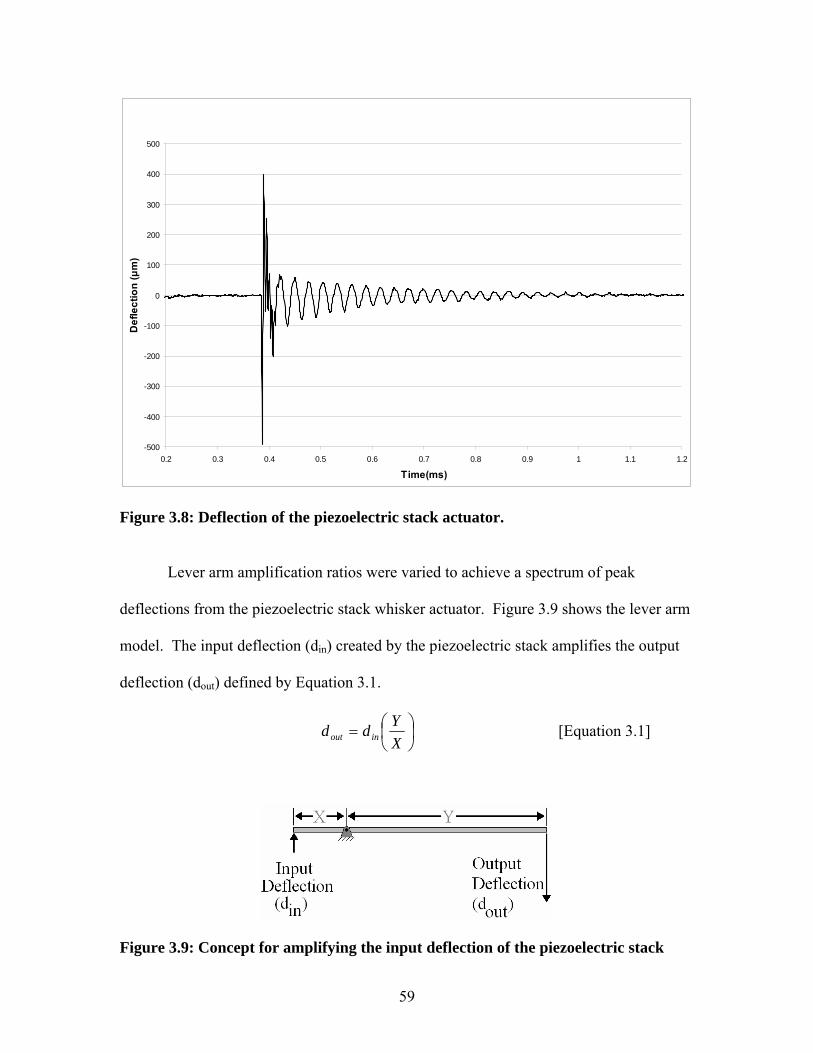
Like the other actuators, the piezoelectric stack actuator was deflected with a 0.2 ms
square wave pulse. However, the actuation voltage was 120 V. The ring out deflection
traces shown in Figure 3.8. The ring out time was found to be approximately 0.35
seconds. The response time was measured to be approximately 0.04 ms. The peak to
peak deflection was found to be 880 μm. In this test the stack actuator was loud enough
that the sound would likely affect the evoked response of the subject significantly,
through knowledge gained from several years of combined expertise. The sound coming
from the device came from the piezoelectric stack actuator.
59
-500
-400
-300
-200
-100
0
100
200
300
400
500
0.2 0.3 0.4 0.5 0.6 0.7 0.8 0.9 1 1.1 1.2
Time(ms)
Def
lect
ion
(μm
)
Figure 3.8: Deflection of the piezoelectric stack actuator.
Lever arm amplification ratios were varied to achieve a spectrum of peak
deflections from the piezoelectric stack whisker actuator. Figure 3.9 shows the lever arm
model. The input deflection (din) created by the piezoelectric stack amplifies the output
deflection (dout) defined by Equation 3.1.
⎟⎠⎞
⎜⎝⎛=
XYdd inout [Equation 3.1]
Figure 3.9: Concept for amplifying the input deflection of the piezoelectric stack

60
The piezoelectric actuator alone deflected 32 μm at 120 V, which is din. The
defection of the end of the lever arm, dout, was calculated for seven different
amplification ratios, from 1 to more than 15. The actual deflection values of the smaller
amplification ratios were measured to be larger than was calculated shown in Figure 3.10.
The actual deflection values of the larger amplification ratios were measured to be
smaller than the calculated deflections, possibly caused from a combination of restriction
of movement in the pivoting areas and the bending of the lever arm.
0
50
100
150
200
250
300
350
400
450
500
0 5 10 15
Amplificaiton Ratio
Def
lect
ion
(μm
)
CalculatedActual
Figure 3.10: Calculated deflections compared actual deflections for the stack actuator.

61
3.4 Whisker Actuator Comparison
Table 3.2 compares the three different types of whisker actuators with respect to ring
out time, response time, maximum peak to peak deflection and relative sound.
The piezoelectric stack whisker actuator possessed the largest deflections and the
shortest response time of the three but its ring out time and audio output were excessive.
The ring out time was over three times the duration of the other actuators. Its long
whisker actuation duration continued affecting the comparison between the whisker
deflection and evoked response beyond the initial evoked response causing difficulties in
interpreting the data. The excessive audio output that came from the stack actuator was
the foremost reason the stack whisker actuator was unacceptable for this application. The
significant noise coming from the device caused a large change in the evoked response
from the rodent.
The piezoelectric bender whisker actuator had a quick response time and a minimal
ring out time. The sound that the actuator induced was an acceptable volume. A large
flaw the piezoelectric bender whisker actuator had was the small deflections for whisker
actuation. The small amplitude of the deflections creates small evoked responses that are
undesirable for signal processing.
The speaker whisker actuator had a slow response time, but it did have a short ring
out time. The relative sound of the actuator was quite small. The speaker actuator was
capable of many different deflection magnitudes.

62
Ring out
Time Response
Time
Peak to Peak
Deflection Relative Sound
(seconds) (ms) (μm) (-)
Speaker 0.15 0.35 116 Minimal Piezoelectric
Bender 0.12 0.075 8 Minimal Piezoelectric
Stack 0.35 0.04 880 Excessive Table 3.2: Comparison evaluation of the speaker, piezoelectric bender and piezoelectric stack actuators.
Preliminary test were aimed at reducing the ring out time of the speaker and the
bender actuators. Those tests revealed that placing a spaced double square wave voltage
input into the actuators dampened their ring out time. The first input square wave
activated the actuator to send the lever arm up. The second input square wave was
designed to occur when the lever arm approached the starting position traveling
downward. The second input wave created an upward force that offsets the downward
momentum of the device and electrically dampened the ring out. Further
experimentation on the timing and magnitude of these damping forces should continue in
order to further reduce the ring out duration.

63
Chapter 4. ELECTRODE ELECTRICAL AND PHYSICAL ANALYSIS
This chapter describes the evaluation of the electrical characteristic and physical
integrity of the electrode arrays. This evaluation of quality was preformed to establish
the reliability of the electrode array fabrication process and to assure that a high quality
electrode array specimen was used for implantation into the subjects.
4.1 Electrode Array Physical Analysis
A photograph of an as fabricated finished electrode array assembly that was
implanted into a rat is shown in Figure 4.1. This electrode array assembly included a
5.75 mm wide, Kapton substrate for implantation. The width of the entire electrode array
assembly pictured in Figure 4.1 was measured to be 54 mm. The length of the electrode
array assembly from the circuit board to the opposite edge of the microfabricated Kapton
portion was 42 mm. The length of just the protruding microfabricated Kapton portion
was 15 mm. The total height of the assembly was measured to be 16 mm. The mass of
the electrode array was measured to be 23 grams. The thickness of the electrode array
was measured at around 40 μm which is at least twice as thin as any of the previous
flexible electrode arrays, fabricated by other groups [Nakauchi K, 2005; Sandison M,
2002], which is expected to provide it with more flexibility.
To make this electrode array an implantable for freely moving animal the device
must be reduced in size. The large mass and size of the electrode array would make it
difficult for a rat to move around. An amplifier and a multiplexer chip must be bonded
onto the Kapton electrode array to allow chronic long term recordings.

64
Figure 4.1: Completed electrode array assembly.
A micrograph of six of the electrodes on the finished electrode array is shown in
Figure 4.2. The black background is the Kapton substrate, the light lines are the gold
leads covered with the SU-8 insulator, and the brighter circles are the gold electrodes.
The circular gold electrodes are the only portion of this electrode array seen below that
was not covered by the SU-8 layer. The visual analysis of the electrode array revealed
that the holes in the SU-8 were aligned with the gold electrodes. Further examination
revealed that there was no cracking of the SU-8 layer and no obvious delaminating of the
gold or SU-8 layers.

65
Figure 4.2: Micrograph of the electrode array surface.
The physically large size and mass of this electrode array restricts it from
consideration for chronic test use. Although the thin inserted portion of the electrode
array increases the time it can be implanted, the electrode array’s size and mass keep it
from being a permanent fixture on the rat’s head. For short term animal testing size does
not matter, but for chronic animal testing it is imperative to reduce the size of the
electrode array and of its associated assembly.
The current photolithography mask used is made by a high resolution printer on a
basic transparency. Using this technology the resolution is approaching its limit for the
electrode array application. The finer the resolution of the photolithography process, the
closer the lines are arranged, the more electrodes can be packed into a given area. Closer

66
spaced electrode arrays will require a new type of lithography techniques. Chrome masks
are the logical first step to increasing mask resolution. This more costly option uses the
same photolithography equipment with the transparency mask, and would be a relatively
easy transition. E-beam lithography [Cunningham W, 2001] is also a feasible option with
capable line widths of 2 μm, but is beyond the availability of the facilities used at this
time.
4.2 Electrode Array Impedance Analysis
The electrical characteristics and integrity of the electrodes were evaluated by
measuring the impedance of each of the 64 gold traces from electrode to connection pad
in a 0.9% saline solution. These electrical attributes are determined prior to
experimentation with rodent subjects. Low impedance electrode arrays are wanted
because impedance is proportional to the Johnson-Nyquist noise. The lower the
impedance is the lower the noise in the signal. Johnson-Nyquist noise is the noise that is
generated by the equilibrium fluctuations of the electric current inside of the electrode
array leads that happens regardless of any applied voltage, due to the random thermal
motion of the electrons [Winipedia, 2005].
Figure 4.3 shows the electrical impedances of the electrode array, rat’s brain, and
evoked response measuring device. When taking the impedance measurements, such as
in table 4.1, the impedance values are that of just the saline and the electrode array.
When taking actual experiments such as in Chapter 5 the impedance is that of the circuit
shown below.

67
Figure 4.3: Electrical circuit of the electrode array the brain of the rat and of the measuring device.
In addition, impedance measurements between traces were conducted to assure
electrical isolation. To assure that there was correct alignment between the electrode
array and the circuit, a probe station linked to an impedance analyzer was used. Each
lead of the electrode array was checked to guarantee that there was no misalignment.
Typical electrode array impedance values (given in kΩ) measured by the technique
described in Appendix C.2 and section 2.4 are presented in Table 4.1. Short circuits
between leads are represented by grey blocks in Table 4.1. Impedance values in the
MΩ range were considered open circuits. The average impedance value of all electrodes
not shorted or broken was 34 kΩ. The impedance values shown below are the electrode
array impedance along with the saline impedance. The standard deviation of the
impedance values was calculated to be 7 kΩ for the 54 electrodes which were not shorted
or open circuit. Impedance maps for all 11 electrode arrays fabricated are given in
Appendix D.

68
Columns Rows A B C D E F G H
(kΩ) (kΩ) (kΩ) (kΩ) (kΩ) (kΩ) (kΩ) (kΩ) 1 28 34 33 30 31 29 29 18 2 25 31 27 24 28 28 19 9000 3 28 14 10000 23 32 28 21 27 4 23 14 27 16 24 24 27 32 5 47 37 34 47 43 40 38 32 6 43 32 28 29 28 148 26 24 7 27 12 25 28 24 180 8000 25 8 26 13 26 12000 25 28 47 23
Table 4.1: Typical electrode array impedance map.
Impedance values between electrode traces directly adjacent to each other were
measured to be 13 MΩ. Impedance values between the two electrode traces that are
furthest from each other were measured to be 20 MΩ. The impedance of the impedance
analyzer system when the probes were not contacted was measured at 25 MΩ.
Gold was used for the electrode array because of its stability in tissue and ease of
manufacturing. It may be possible to improve this impedance by using platinum black
deposits for the electrodes contact area [Grumet AE, 2000]. Increasing the surface area
of the electrode pads by surface roughening could be valuable in making small changes in
decreasing the impedance of the electrode array leads. The impedance of the electrode
array may be changed substantially by varying the size of the electrodes. The electrode
here has a low impedance value because it has relatively large electrodes.
Figure 4.4 illustrates the nominal relationship between the recording frequency
and the impedance of a single electrode from the electrode array. The electrode array
alone has a consistent value of impedance across the frequency range of 40 Hz to 3 kHz.
The saline has a capacitive nature in that the impedance increases as the frequency

69
decreases. The electrode array and saline impedance values are not the value of the super
position of the saline and electrode array impedance values individually tested.
1
10
100
1000
10000
100000
1000000
0 500 1000 1500 2000 2500 3000
Frequency (Hz)
Impe
danc
e (O
hms)
Electrode OnlySaline OnlySaline and Electrode Array
Figure 4.4: Electrode array, saline, and saline and electrode array impedance values depending on frequency for the frequency range of 40 Hz to 3 kHz.
Observations of decreasing impedances with time occurred while recording
impedances from the electrode arrays through saline. Figure 4.5 displays impedance
values and their time dependence for three input voltages, 1 V, 100 mV and 10 mV. The
impedance decreased for all three input voltages during the 10 minute test period as they
asymptotically approached their ultimate values. The phenomenon can be due to the
electrochemical change of the saline when a voltage was applied. The impedance value
change for the 10 mV input voltage was much larger than the higher input voltages, but
the percent change between the beginning values to the 10 minute values correlate
closely.

70
0
20
40
60
80
100
120
140
160
180
0 100 200 300 400 500 600 700
Time (seconds)
Impe
danc
e(kO
hms)
10mV
100mV
1V
Figure 4.5: Electrode array impedance values varying with time for 1V, 100mV, and 10mV input voltages.
To determine the effect that saline solution on the overall impedance of the
electrode array, an impedance test and a resistance test were conducted on a saline puddle
without the array at 500 mV. In Table 4.2 the distance between conducting points in a
saline solution puddle reduced both the impedance and the resistance. For distances
smaller than 0.25 inches there was little to no difference in impedance, i.e., all values
were measured between 1400 Ω and 1500 Ω. The actual distance in the saline solution
during the testing of an electrode array with the impedance analyzer would be between
0.06 and 0.5 inches. Hence it is not expected that variations in the saline solution
distances during impedance testing caused any variation in the results since these
distances are within the consistent impedance range of these tests.
71
Distance in Saline Solution Resistance Impedance
(in) (Ω) (Ω) 4 2910 3210 3 2100 2360 2 1550 1870
1.4 1310 1610 0.75 117 1470 0.25 118 1450
Table 4.2: Variation of impedances within saline solution puddle with respect to distance.
Each component of the electrode array was measured to determine its impedance
value at 1 V and 1 kHz. The results for the individual components as well as series of
combined components impedances are show are shown in Table 4.3. Each of the
components themselves did not have a large contribution to the overall impedance. The
stacked up values for all of the components and saline solution are less than 10% of the
total impedance of the entire electrode array set up. The impedance of the saline and
microfabricated portion of the electrode array alone was found to be very close to that of
entire electrode array set up.
Components
Involved
Pin connector
Circuit Board
Zebra Connector
Microfabricated Portion of the
Electrode ArraySaline
Solution Impedancex <1Ω x <1Ω x ~200Ω x ~50Ω x ~1500Ω x x <1Ω x x ~35000Ω x x x x x ~35000Ω
Table 4.3: Impedance values for different components and compiled components.

72
4.3 Electrode Array Durability
With the inherent advantages of a flexible array, it is incumbent upon the designer
to assure that this flexing does not render the electrode array unusable. Hence, the
mechanical durability of the electrode array assembly in bending was tested by wrapping
the electrode end of the electrode array around dowel pins with varying diameters and
subsequently testing the electrical integrity of the array. A picture of the configuration of
the bending is shown in Figure 4.6, where the electrode array is rolled around a 1/16 inch
radius dowel pin normal to the direction of the connecting leads. The end of the
electrode array was taped to the dowel pins.
Figure 4.6: Mechanical durability test of an electrode array by bending around a 1/16 inch dowel pin.
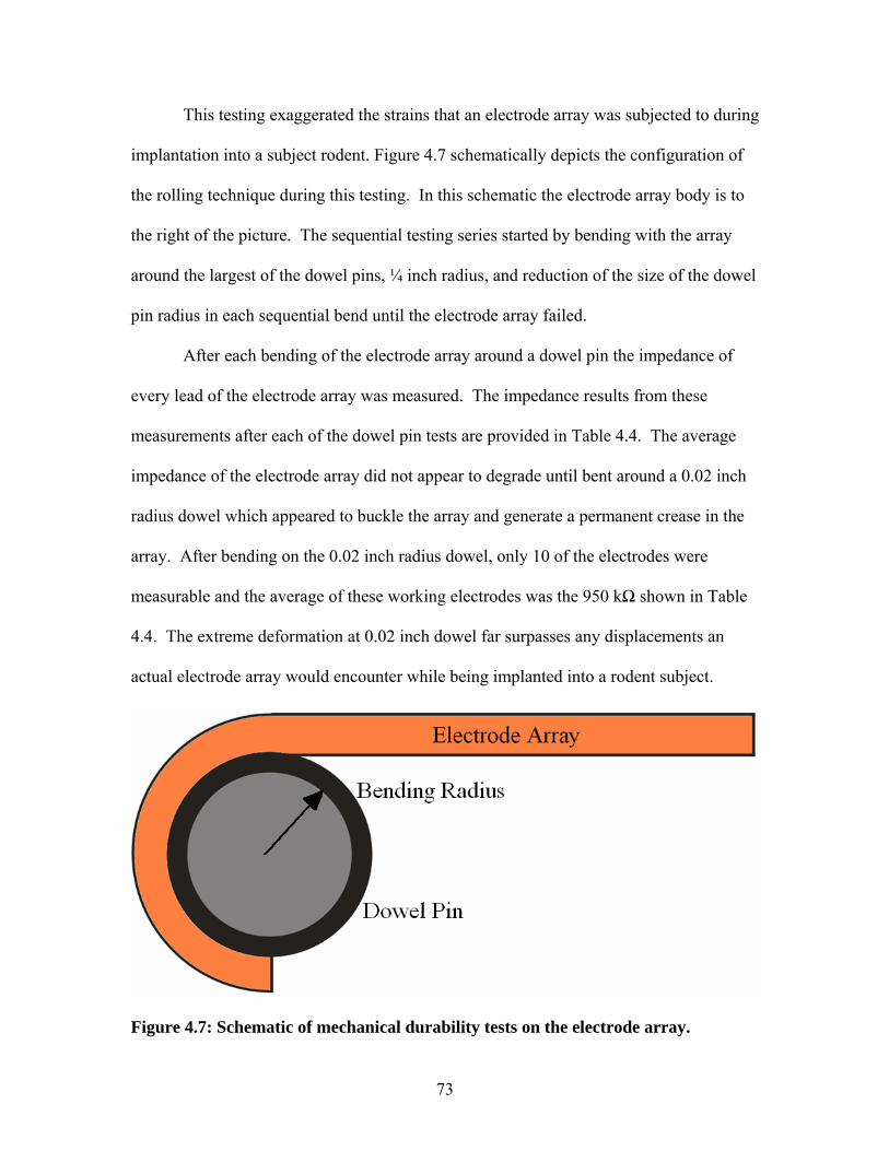
73
This testing exaggerated the strains that an electrode array was subjected to during
implantation into a subject rodent. Figure 4.7 schematically depicts the configuration of
the rolling technique during this testing. In this schematic the electrode array body is to
the right of the picture. The sequential testing series started by bending with the array
around the largest of the dowel pins, ¼ inch radius, and reduction of the size of the dowel
pin radius in each sequential bend until the electrode array failed.
After each bending of the electrode array around a dowel pin the impedance of
every lead of the electrode array was measured. The impedance results from these
measurements after each of the dowel pin tests are provided in Table 4.4. The average
impedance of the electrode array did not appear to degrade until bent around a 0.02 inch
radius dowel which appeared to buckle the array and generate a permanent crease in the
array. After bending on the 0.02 inch radius dowel, only 10 of the electrodes were
measurable and the average of these working electrodes was the 950 kΩ shown in Table
4.4. The extreme deformation at 0.02 inch dowel far surpasses any displacements an
actual electrode array would encounter while being implanted into a rodent subject.
Figure 4.7: Schematic of mechanical durability tests on the electrode array.

74
Bending Radius
Impedance averages
Measurable Electrodes
Electrodes with Significantly Different Impedances than the Previous Test
(inches) (kΩ) 1/4 30 45 0 5/32 30 45 0 1/8 30 45 0 3/32 30 45 0 1/16 30 45 0 0.02 950 15 45 (all)
Table 4.4: Electrical analysis after mechanical durability test on the electrode array.
Bending the electrode array in this manner around the dowel pins exerts a tensile
strain onto the outside of the electrode array, where the gold circuit lies. The electrical
failure of the electrode array was caused by the strain induced in the gold. Because the
gold is so thin, (300 nm) the Kapton (25 μm) and the SU-8 (13 μm) were assumed to be
the major structural contributor in the bending strains. The strain acting on the outside
edge of the Kapton was considered to be equal to the uniform strain on the adjacent gold.
It was assumed that the force put on the substrate to curl it around the dowel pin
caused bending only and no stretching. The strain in the gold )( goldε is represented by:
( )ooo
o
o
ogold R
dR
RdRR
RRR
RR=
−+=
−=
−=
πππ
ε2
22 [Equation 4.1]
where R is the radius to the gold and the location of maximum tensile strain. oR is the
radius to the neutral axis of the Kapton. Hence, oRπ2 is the length of the neutral axis at
any elastically strained state, i.e. the unstrained state. Rπ2 is the length of the outside
edge of the Kapton as well as the gold when it is strained. The distance from the neutral
axis of the composite to the gold film was represented by d and assumed to be 6 μm.
Figure 4.8 is a representation of the strains in the Kapton film and the gold circuit during
bending around a dowel pin radius.
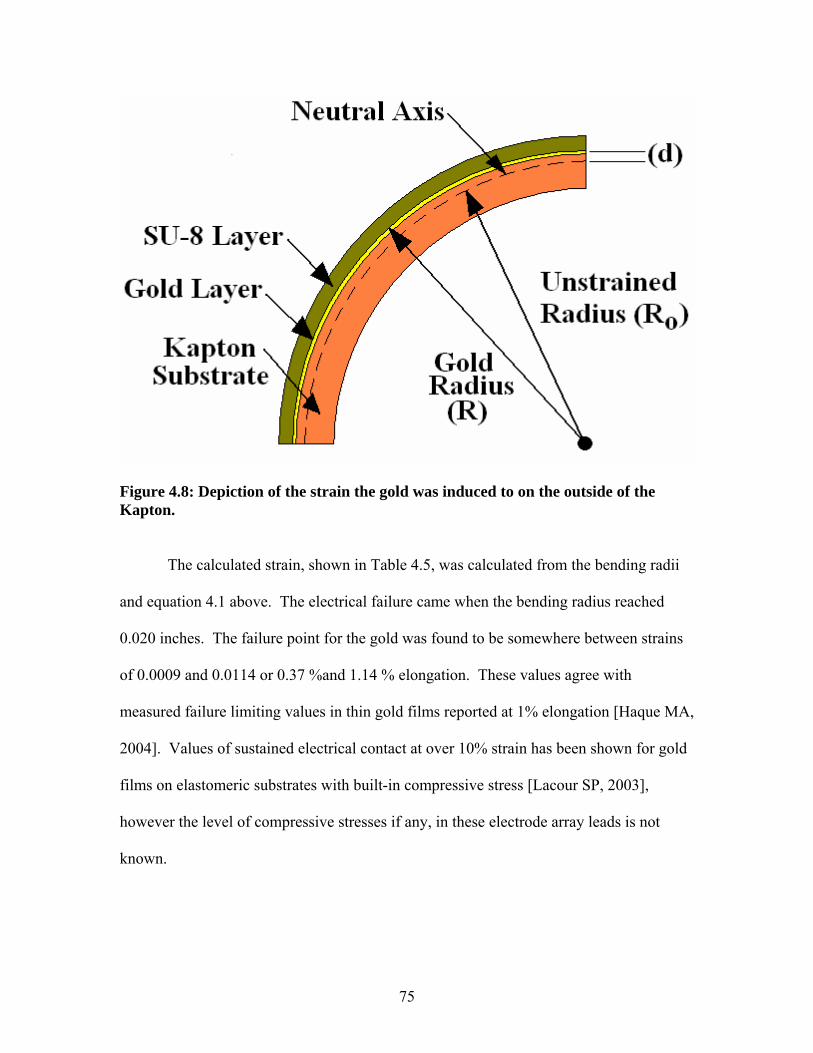
75
Figure 4.8: Depiction of the strain the gold was induced to on the outside of the Kapton. The calculated strain, shown in Table 4.5, was calculated from the bending radii
and equation 4.1 above. The electrical failure came when the bending radius reached
0.020 inches. The failure point for the gold was found to be somewhere between strains
of 0.0009 and 0.0114 or 0.37 %and 1.14 % elongation. These values agree with
measured failure limiting values in thin gold films reported at 1% elongation [Haque MA,
2004]. Values of sustained electrical contact at over 10% strain has been shown for gold
films on elastomeric substrates with built-in compressive stress [Lacour SP, 2003],
however the level of compressive stresses if any, in these electrode array leads is not
known.

76
Bending Radius Unstrained Radius Strain (inches) (inches) (in/in) (% in/in) 0.250 0.251 0.0009 0.09 0.1563 0.157 0.0015 0.15 0.1250 0.126 0.0019 0.19 0.0938 0.094 0.0025 0.25 0.0625 0.063 0.0037 0.37 0.0200 0.021 0.0114 1.14
Table 4.5: Calculated strain for electrode array and varied bending radii.
4.4 Electrode Array Statistical Analysis
Eleven electrode arrays were constructed and impedance tested. The total average
of the impedance values for all eleven electrodes was 33 kΩ with a standard deviation of
13 kΩ. The impedance values for these electrode arrays were found to be small because
of its large area of the electrodes. The average number of breaks in the electrical leads
was 9 and the average number of electrical shorts was 2. The average number of working
electrodes for all electrode arrays was measure to be 53 out of 64 total electrodes.

77
Chapter 5. ELECTRODE ARRAY ANIMAL TESTS
In this chapter the results from implanting the electrode arrays into subject rodents
are reviewed. As discussed earlier, the electrode array gathered the evoked responses of
the rats, obtained during whisker deflections using the whisker. During these tests, the
consistency, resolution, and information encoded in the evoked response was the central
focus. The evoked response voltages measured were obtained from the electrode arrays
positioned on the surface of the rodent’s brain called the whisker barrels. The electrode
arrays were implanted directly over the whisker barrels, as in Figure 2.12, to establish the
spatial location of the barrels on the rat’s brain. The electrode array also assisted in
researching the correspondence between the whisker barrels and whisker actuation.
5.1 Evoked Response Recordings
The typical whisker actuation response is shown in Figure 5.1 for one electrode
out of a 64 electrode array. The trace is the voltage output from the surface of the dura,
measured after the actuation of the rodent’s whisker as described earlier. From the left,
the first spike is an artifact associated with the stimulation equipment and not a part of the
cordical wave. These traces include peaks and minimums which are designated as the
P1, N1, P2, and N2 characteristics of the response which are clearly distinguishable with
a good signal-to-noise ratio. Although not discussed here, the interpretation of the
significance of these characteristics is the subject of research in the medical community.
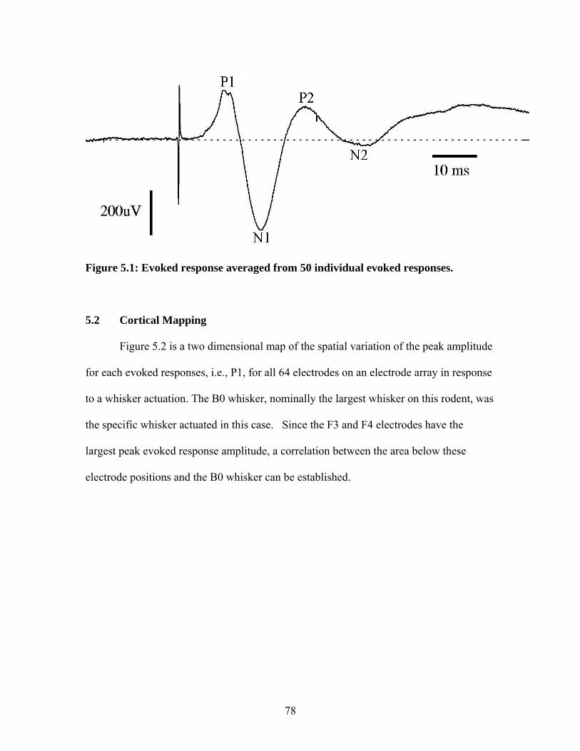
78
Figure 5.1: Evoked response averaged from 50 individual evoked responses.
5.2 Cortical Mapping
Figure 5.2 is a two dimensional map of the spatial variation of the peak amplitude
for each evoked responses, i.e., P1, for all 64 electrodes on an electrode array in response
to a whisker actuation. The B0 whisker, nominally the largest whisker on this rodent, was
the specific whisker actuated in this case. Since the F3 and F4 electrodes have the
largest peak evoked response amplitude, a correlation between the area below these
electrode positions and the B0 whisker can be established.

79
Figure 5.2: Two dimensional map of evoked responses for 24 different whiskers.
5.3 Varying Whisker Deflection Evoked Responses
The input voltage for the whisker actuating speaker was varied in a series of tests to
obtain a spectrum of whisker deflections. The rat’s evoked responses to the seven
different speaker whisker actuator deflections along with one piezoelectric bender
whisker actuator deflections are compared in Figure 5.3. The magnitude of the evoked
response is shown on the left and the magnitude of the actuators deflection, shown in
Figure 3.2 and Table 3.1, is labeled on the right. As in Figure 5.1, the first spike was not
a response of the rodent, but an artifact of the stimulus from the equipment used.
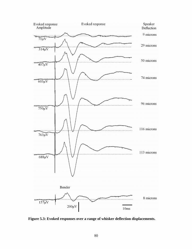
80
Figure 5.3: Evoked responses over a range of whisker deflection displacements.

81
Figure 5.4 compares the P1 characteristic of the evoked response traces presented
above in Figure 5.3 with the whisker deflections for each test. It appears that the
amplitude of the evoked response and the actuator deflection is linearly related in the data
range tested over this range. A linear least-square fit of the speaker data is provided in
Figure 5.4 of the data taken from tests with the speaker whisker actuator. The rat does
have a response to the sound of the actuator. The values are the superposition values of
the combination of the evoked response of the sound the speaker makes as well as the
evoked response to the movement the speaker makes.
0
100
200
300
400
500
600
700
800
0 20 40 60 80 100 120
Speaker Deflection (μm)
Evo
ked
Res
pons
e Am
plitu
de (μ
V)
SpeakerBender
Figure 5.4: Evoked response amplitudes compared to deflection amplitudes.

82
Chapter 6. CONCLUSIONS
6.1 Whisker Actuator Conclusions
Section 3.4 compares the characteristics of the different types of whisker actuators
made. The important whisker actuator characteristics that were evaluated were the
relative audio output, deflection, response time, and duration of ring out time. The
differences of the three actuators are summarized in Table 3.2.
The speaker whisker actuator was tested to be the best alternative for a whisker
deflecting device. Although the speaker whisker actuator had a slow response time
relative to the other actuators, it did have a small ring out time. It had a wide range of
deflections that were easily obtained for varying deflection experiments. The small audio
click of the speaker whisker actuator had a minimal effect on the evoked response of a
rodent subjects.
6.2 Electrode Array Conclusions
The design, fabrication, as well as electrical and physical verification testing of a
flexible polymer based electrode array have been demonstrated. Once the clean room
and assembling fabrication steps were completed, the visual assessment and electrode
impedance measurement evaluation were conducted in order to assure that the electrode
array was acceptable to implant into a rodent.
The portion of the electrode array that was implanted was designed and fabricated
to be approximately 50 μm thick and a width of 5.75 mm. The width of the electrode
array was cut to be only slightly larger than the actual electrode coverage width to

83
facilitate insertion into the smallest opening in the rodent’s skull as possible. The
electrode array had an electrode coverage area or 5.4 mm by 5.4 mm, with an electrode
density of over 200 electrodes per square centimeter. The resulting electrode array weight
was measured to be 23 grams. The physical testing presented in section 4.2 verified that
the electrode array was robust enough to withstand the adjusting and manipulation of
implantation of the device. The extreme deflections encountered in the tests described
there are far beyond any application of the array on rodents.
The electrical testing of the electrode array assured that each of the 64 leads in the
electrode array was possessed the continuity for transferring signals to the recording
devices. The average impedance value of non-shorted, non-broken leads for 11 electrode
arrays was 33 kΩ with a standard deviation of 13 kΩ. The average number of working
electrodes on an electrode array was 53.
Although formidable the first time, the photolithographic process should allowed
virtually any electrode pattern to be applied over the two dimensional array, regardless of
size and shape. Furthermore, it is expected that once scaled up these devices could be
mass produced at relatively low cost.
6.3 Electrode Array Animal Testing Conclusions
The electrode array was stiff enough to retain its form and thin enough to be
inserted between the dura and the skull of the rat. The robustness of the electrode array
was further proven when observed to be undamaged after experiments on rats. The
electrode array traces retrieved evoked response data that possessed response
characteristics P1, N1, P2, and N2 components with good signal to noise ratio. A linear

84
correlation between the deflection of the whisker actuator and the evoked response
amplitude was discussed in section 5.3.
This electrode array appeared to reduce the trauma to the animals in comparison
to penetrating electrodes [Barth D, 1990; Rennaker R, 2005; Rousche P, 1998; Rousche
P, 2001; Takeuchi S, 2003; Tsai M, 2003] , since the latter required removal of large
portions of the skull.
6.4 Whisker Actuator Recommendations
Further investigation of the response times of the whisker actuators should be
done. To properly access the response time for the evoked response of the rat, it is
important to know when the actual whisker actuation occurs. When this is known there
will be less importance on finding an actuator with a quick response time and more
importance on when the whisker actuation happens.
6.5 Electrode Array Fabrication Recommendations
The current thickness of 50 μm for the implantation portion of the electrode array
worked effectively for the Sprague-Dawley rodent tests. This thickness could be altered
either up or down depending upon the application. Electrode array thickness changes
may be accomplished by using a different Kapton substrate or SU-8 formula. A 75 μm
thick electrode array has been tested in a rat, instead of the current 50 μm thick electrode
array. The greater stiffness of the 75 μm electrode array created a scenario where the
electrode array could not bend enough to be implanted correctly and cut the dura, so was
not acceptable. The different substrate thicknesses alter the exposure times needed for
the photolithographic techniques.

85
The 8 by 8 electrode array grid was constructed to cover the majority of the
whisker barrel area. This arrangement may be changed to increase the number or
increase the density of the electrodes. A pattern where leads access the electrodes
radially could result in an increase in electrode density, but would not be applicable to
electrode arrays that are inserted like the one presented with a minimum cross section for
insertion.
6.6 Electrode Array Animal Testing Recommendations
A key advantage of the electrode array presented is that it can be inserted in a slit
made in the skull and does not require large portions of the skull to be removed. The
biocompatibility of the complete electrode array should be tested in long term
implantations, to see if the rodent’s body rejects the device.
Remotely recording information from an electrode array using a transmitting
device surgically implanted within the subject is a long term vision for chronic animal
testing. This self-contained device would allow the recording of evoked response from
free roaming animals in a more natural environment, and adds new dimensions to the
array of biological monitoring and stimulation that exist today.

86
REFERENCES
American Piezo Ceramics, Inc. http://www.americanpiezo.com Accessed September 12, 2005. Barth, Daniel S., Di, Shi. “Three-Dimensional Analysis of Auditor-Evoked Potentials in Rat Neocortex,” Journal of Neurophysiology, 1990; 64(5):1527-1536. Bragin A, Hetke J, Wilson CL, Anderson DJ, Engel Jr. J, Buzsaki G Multiple site silicon-based probes for chronic recordings in freely moving rats: implantation, recording and histological verification . Journal of Neuroscience Methods. 2000; 98(2):77-82 Cunningham W, Mathieson K, McEwan FA, Blue A, McGeachy R, McLeod JA, Morris-Ellis C, O’Shea V, Smith, KM., Litke, A., Rahman, M. “Fabrication of microelectrode arrays for neural measurements from retinal tissue,” Journal of Physics D: Applied Physics, No. 34, 2001: 2804-2809. Devilbiss DM, Waterhouse BD. “Determination and quantification of pharmacological physiological, or behavioral manipulations on ensembles of simultaneously recorded neurons in functionally related neural circuits. Journal of Neuroscience Methods. 2002; 121(2): 181-98 Franowicz, MN, Barth DS. “Comparison of Evoked Potentials and High-Frequency (Gamma-Band) Oscillating Potentials in Rat Auditory Cortex,” Journal of Neurophysiology, 1995; 74(1):96-112. Gonzalez C; Rodriguez M. “A flexible perforated microeletrode array probe for action potential recording in nerve and muscle tissues,” Journal of Neuroscience Methods, 1997; 72(2):189-195. Grumet AE, Wyatt JL, Rizzo JF. “Multi-electrode stimulation and recording in the isolated retina,” Journal of Neuroscience Methods. 2000; 1010(1): 31-42. Grumet, Andrew E., Wyatt,, Jr., John L., Rizzo, Joseph F. III, “Multi-electrode stimulation and recording in the isolated retina,” Journal of Neuroscience Methods, 2000; 1010(1):31-42. Haque MA, Saif MTA. “Deformation mechanisms in free-standing nanoscale thin films: A quantitative in situ transmission electron microscope study,” Proceedings of the National Academy of Sciences of the USA, 2004; 101(17): 6335-6340. Harris JA, Petersen RS, Diamond ME. “Distribution of tactile learning and its neural basis,” Proceedings of the National Academy of Sciences of the USA, 1999; 96(13): 7587-7591.
87
Huber R, Ghilardi MF, Massimini M, Tononi G. Local sleep and learning. Nature. 2004; 430: 78-81. Hung A; Zhou D; Greenberg R; Judy JW. “Micromachined Electrodes for Retinal Prostheses,” IEEE-EMBS Special Topic Conference on Microtechnologies in Medice and Biology, 2002: 75-79. Jones MS, Barth DS. Spatiotemporal organization of fast (>200Hz) electrical oscillations in rat Vibrissa/Barrel cortex. J Neurophysiology 1999; 82(3):1599-1609. Kapton, Summary of Properties, http://www.dupont.com/kapton/general/H-38492-2.pdf Accessed August 17, 2005 Kipke Dr, Vetter RJ, Williams JC, Hetke JF. Silicon-substrate intracortical microelectrode arrays for long-term recoding of neuronal spike activity in cerebral cortex. Transactions on Neural Systems and Rehabilitation Engineering. 2003; 11(2): 151-155. Kreuz JA, Milligan SN, Sutton RF. http://www.dupont.com/kapton/applications/fpc-tab.html Accessed August 15, 2005 Krupa DJ, Brisben AJ, Nicolelis MAL, “A multi-channel whisker stimulator of producing spatiotemporally complex tactile stimuli,” Journal of Neuroscience Methods, 2000; 104:199-208. Kublik E, Musia P, Wrobel A. “Identification of principal components in cortical evoked potentials by brief surface cooling.” Journal of Clinical Neurophysiology. 2001; 112(9): 1720-1725. Kyriazi H, Simons D. http://www.neurobio.pitt.edu/BARRELS/ Accessed August 9, 2005 Lacour SP, Wagner S, Huang Z, Suo Z. “Stretchable gold conductors on elastomeric substrates.” Applied Physics Letters. 2003; 82(15): 2404 McKenney DJ and Numakura DK. Numakurahttp://www.circuitree.com/CDA/ArticleInformation/coverstory/BNPCoverStoryItem/0,2135,8787,00.html Accessed August 18, 2005. Mirabella G, Battiston S, Diamond ME. “Integration of Multiple-whisker Inputs in Rat Somatosensory Cortex.” Cerebral Cortex. 2001; 11(2): 164-170. Nakauchi K, Fujikado T, Kanda K, Morimoto T, Choi JS, Ikuno Y, Sakaguchi H, Kamei M, Ohji M, Yagi T, Nishimura S, Sawai H, Fukuda Y, Tano Y. Transretinal electrical stimulation by an intrascleral multichannel electrode array in rabbit eyes. Graefe’s Archive Clinical Experimentation of Ophthalmology. 2005; 243: 169-174.

88
Herzog, Ek, Bahr DF. http://www.mme.wsu.edu/~reu/PDFs/Herzog.pdf Accessed October 20, 2005. Normann, Richard A., “Microfabricated Electrode Arrays for Restoring Lost Sensory and Motor Functions” Digest of Technical Papers-The 12th International Conference on Solid-State Sensors, Actuators and Microsystems, 2003; 2: 959-962 Patil PG, Camena JM, Nicolelis MAL, Turner DA. Ensemble Recordings of Human Subcortical Neurons as a Source of Motor Control Signals for a Brain-Machine Interface. Neurosurgery. 2004; 55: 27-38. Petersen, Rasmus S., Diamond, Mathew E. “Spatial-Temporal Distribution of Whisker-Evoked Activity in Rat Somatosensory Cortex and the Coding of Stimulus Location,” Journal of Neuroscience, 2000; 20(16): 6135-6143. Rector DM, Topchiy IA, Carter KM, Rojas MJ. “Local functional state differences between rat cortical columns,” Brain Research, 2005; 1(1047): 45-55. Rennaker RL., Ruyle AM., Street SE, Sloan, A. M. “An economical multi-channel cortical electrode array for extended periods of recording during behavior” Journal of Neuroscience Methods, 2005; 142(1): 97-105. Rousche PJ.; Normann RA. “Chronic recording capability of the Utah Intracortical Electrode Array in cat sensory cortex,” Journal of Neuroscience Methods, 1998; 82(1): 1-15. Rousche PJ, Petersen RS, Battiston S, Giannotta S, Diamond ME. Examination of the spatial and temporal distribution of sensory cortical activity using a 100-electrode array. J Neuroscience Methods. 1999; 90(1): 57-66. Rousche, Patrick J., Pellinen, David S., Pivin, David P., Williams, Justin C., Vetter, Rio J., Kipke, Daryl R. “Flexible Polyimide-Based Intracortical Electrode Arrays with Bioactive Capability,” IEEE Transactions on Biomedical Engineering, 2001; 48(3):361-371. Sachdev RN, Champney GC, Lee H, Price RR, Pickens DR 3rd, Morgan VL, Stefansic JD, Melzer P, Ebner FF. “Experimental model for functional magnetic resonance imaging of somatic sensory cortex in the unanesthetized rat,” Neuroimage, 2003, 19(3): 742-750. Sachs HG; Schanze T, Wilms M, Retzos A, Brunner U, Gekeler F, Hesse L. “Subretinal implantation and testing of polyimide film electrodes in cats,” Graefe’s Archive for Clinical and Experimental Ophthalmology Incorporating German Journal of Ophthalmology, 2004, 10.1007/s00417-004-1049-x.

89
Sandison, M, Curtis, A. S. G., Wilkinson, C.D.W. “Effective extra-cellular recording from vertebrate neurons in culture using a new type of micro-electrode array,” Journal of Neuroscience Methods, 2002; 114(1): 63-71. Shen H, Greene AS, Stein EA, Hudetz AG. “Functional Cerbral Hypermia is Unaffected by Isovolemic Hemodilution”, Journal of Anesthesiology. 2002; 96(1), 142-147. SU-8 Resist, http://www.microchem.com/products/su_eight.htm Accessed August 17, 2005. Takeuchi S, Suzuki T, Mabuchi K, Fujita H. 3D flexible multichannel neural probe array. Journal of Micromechanics and Microengineering. 2004; 14: 104-107 Tsai M, Yen C. “A simple method for fabricating horizontal and vertical microwire arrays,” Journal of Neuroscience Methods, 2003; 131(1): 107-110. Takeuchi, Shoji, Suzuki, Takafumi, Mabuchi, Kunihiko, Fujita, Hiroyuki. “3D flexible multichannel neural probe array,” Journal Micromechanics and Microengineering, 2003; 14: 104. Winipedia. http://en.wikipedia.org/wiki/Thermal_noise Accessed November 30, 2005
Zebra Elastomeric Connectors. http://www.fujipoly.com Accessed August 18, 2005.

90
APPENDICES

91
Appendix A: Overview of Electrode Array Fabrication Steps The fabrication of Electrode array is divided into microfabrication steps and macrofabrication steps below. Each of the steps is then discussed detail later. All microfabrication processes were conducted in a class 1000 clean room in order to assure that surface contamination did not contribute to defects in the final product.
1. Manufacturing Materials and Equipment
Microfabrication Steps
2. Preparing Kapton and bonding it to glass slides 3. Plasma Etch Kapton 4. Sputter TiW and Au onto Kapton Film 5. Plasma Etch Kapton and Gold Sheet 6. TiW and Au Photolithography Patterning 7. Plasma Etch Kapton and Patterned Gold 8. SU8 Fabrication Steps
Macrofabrication Steps
9. Drill alignment holes 10. Constructing an Electrode Array 11. Cutting Electrode Array into Final Form

92
Appendix B.1: Manufacturing Materials and Equipment
Materials Kapton Sheet 100HN, 25 μm Thick, made by Dupont Kapton tape, 20mm Wide, 25 μm Thick, made by Dupont Glass slide, 25mm x 75mm x 1mm, made by Fisher Scientific Single Sided Razor Blade ChemWipe Disposable Towels Wafer Tape, 25 mm Wide Gold Sputtering Target Titanium-Tungsten Sputtering Target 1/8 inch Dowel Pin Salt Nitrile Gloves Zebra Connector 500 mL Nalgene Bottle Cleanroom chemicals IPA (Isopropanol) Acetone Liquid Nitrogen Deionized Water Source Canned Air Hexamethyldisilazane made by Fluka AZ5214-EIR photoresist, made by Clariant 30% Hydrogen Peroxide AZ400K Developer Gold Etch SU-8 2010, made by MicroChem Equipment Class 1000 Clean Room Wafer Handling Tweezers 2 Hotplates PE-2000 Plasma Etching System, South Bay Technology INC BOC Edwards AUTO 306 Sputtering System Disposable Pipettes Canned Air Spin Coater Photolithography Machine Digital Scale Agilent 4294A precision impedance analyzer Abrasive Metal Grinder Drill Press Prefabricated Alignment Jig Prefabricated Drilling Jig

93
Appendix B.2: Step 2. Preparing Kapton and bonding it to glass slides
This step describes cutting the Kapton into usable rectangles and taping them to glass slides.
1. Clear working space on the clean bench 2. Assemble supplies on the clean bench:
a. Kapton film sheet b. Kapton tape c. Glass slide d. Razor blade
3. Put on nitrile gloves 4. Inspect Kapton sheet for visible defects or excessive scratches and reject if
defective 5. Cut Kapton into working size
a. Place Kapton sheet down flat onto the bench b. Place glass slide on top of the Kapton so that glass slide extends past the
sheet in the longest dimension by approximately 3 mm, but is aligned with the edge of the Kapton sheet in the width dimension (See Figure B.2.1).
c. Cut along two edges with a razor blade as shown in Figure B.2.1.
Figure: B.2.1: Cutting Kapton
6. Tape Kapton on slide a. Cut Kapton tape into 20 mm strips
i. Successful runs have also been done by cutting the Kapton in strips exactly the width of the slides to completely hold down the Kapton’s edge
b. Place tape across the width of each end of the Kapton film with an overlap from 2mm to 4mm in contact with the Kapton film.
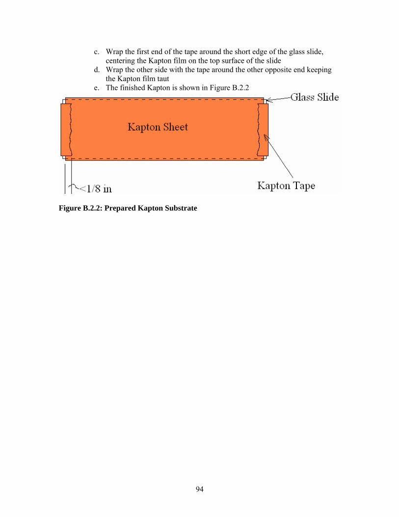
94
c. Wrap the first end of the tape around the short edge of the glass slide, centering the Kapton film on the top surface of the slide
d. Wrap the other side with the tape around the other opposite end keeping the Kapton film taut
e. The finished Kapton is shown in Figure B.2.2
Figure B.2.2: Prepared Kapton Substrate

95
Appendix B.3: Step 3, 5 & 7. Plasma Etching
These plasma etching steps clean the surface of substrate for steps 4, 6, and 8. Note: Plasma etching should be accomplished immediately before steps 4, 6, and 8.
1. Preparation a. Fill out the Plasma etching log with full name, time, date, advisor, account
number, phone number, email address, power and pressure settings b. For step 2, clean Kapton substrate using a IPA wetted ChemWipe
i. Let slide air dry for 30 seconds ii. For steps 4 and 6, the surface should not be cleaned with any IPA
because it will remove the gold film or the gold circuit. 2. Turn on main power switch 3. Press the VENT button to vent the chamber to the atmosphere 4. When pressure is less than 50 mtorr, lift the chamber lid and make sure it stays
open. Note that this lid often will often close by itself. 5. Place Kapton slides into chamber
a. It is possible to load as many slides as will fit on the metal electrode b. Be sure that the slides do not cover the front left hole on the electrode
platter, because that is where the Oxygen is introduced into the chamber. 6. Close the chamber lid 7. Press the VENT button again to turn it off 8. Press the PUMP button to begin the vacuum pump
a. Pump the chamber down until the pressure is below 50 mtorr. This will usually take about 10 minutes to accomplish
9. Record the base pressure. 10. Press GAS 2 (Oxygen) button to introduce oxygen into the chamber 11. Adjust oxygen setting dial manually to bring chamber pressure to between 125
and 150 mtorr, visually checking while adjusting the dial. 12. After the chamber reaches and stable pressure , set the clock timer for 3 minutes 13. Press RF POWER to turn on plasma power 14. Ramp up FORWARD POWER knob to between 105 and 110 Watts 15. Adjust REFLECTIVE POWER knob so that it is minimized and the purple plasma
glow above the electrode platter is maximized a. The forward power minus the reflected power should be 100 Watts +/- 2
Watts 16. After the timer has turned the RF power off automatically, press GAS 2 (Oxygen)
button to turn off the oxygen coming into the camber 17. Press the PUMP button to turn off the vacuum pump 18. Press VENT button to vent chamber 19. If oxidation furnace is not in use, close the valve on the oxygen tank 20. After chamber has vented to atmospheric pressure, lifted open chamber 21. Remove slides with wafer grabbers and inspect for surface flaws 22. Put slides into wafer boxes 23. Close lid of plasma etcher 24. Press vacuum button to turn vacuum on for around 30 seconds

96
25. Flip power switch to turn off power to the plasma etcher. 26. Plasma etching is complete

97
Appendix B.4: Step 4: Sputter TiW and Au onto Kapton Film
We will be sputtering 5 nm of Titanium-Tungsten (TiW) and 300 nm of Gold (Au) onto the Kapton Substrate using the BOC Edwards AUTO 306 Sputtering System.
1. Preparation a. Fill out sputtering log with pre sputtering information
i. For target #1 we use: 1. TiW 2. DC sputtering 3. 7.5 x 10⁻³ torr for Chamber Process Pressure 4. 2 minute shield sputtering time 5. 51 second open shutter time
ii. For target #2 we use: 1. Au 2. DC sputtering 3. 7.5 x 10⁻³ torr for Chamber Process Pressure 4. 2 minute shield sputtering time 5. 51 second open shutter time
b. Put on nitrile gloves 2. Prepare samples as follows in Appendix B.2 3. Plasma Etch as follows in Appendix B.3 4. Vent sputtering chamber by pushing the VENT button on the AUTO-306
controller 5. The display will indicate SEALED when the vacuum chamber reaches
atmospheric pressure. 6. Pull door handle to open the chamber door
a. Minimize time that the chamber door is open to reduce particles and moisture from entering the chamber
7. Load Au and TiW sputtering targets using work bench side instructions a. Lay out a large ChemWipe on the surface in front of the chamber door b. Remove shuttering disk for sputtering gun #1 in rear c. Rotate the shutter support arm out of the way by pressing the shutter I
control button d. Lift the shield vertically off the sputtering gun and set down on the clean
ChemWipe e. Unscrew the six Allen-head screws that are holding the copper clamp ring. f. Remove the clamping ring g. Remove the TiW target from the plastic bag and center it on the sputtering
gun h. Replace the clamping ring over the TiW target i. Lightly tighten the six Allen-head screws in a star pattern j. Place the shield over the sputtering gun while aligning the middle length
slot with the shield screw. k. Assure that the shield is level and aligned with the sputtering gun

98
l. Lightly, hand tighten the front shield screw. m. Rotate the shutter support arm back over the sputtering gun by pressing
the shutter #1 button n. Install the shutter disk shutter by hand tightening the screw to the shutter
threw the lever arm o. Repeat steps b threw n for gold and sputtering gun #2
8. Attach slides to the solid rotary work holder a. Remove slides from plasma etcher b. Cut wafer tape into pieces to attached the slides
i. Use razor blade to cut wafer tape along the center of the tape and again across the tape to make 12 mm by 40 mm pieces of wafer tape
c. With the Kapton side up, arrange the slides on top of the rotary work holder
d. Using the precut wafer tape, attach the slides down to the rotary work holder
i. Tape down slides on both sides of the short end of the slide ii. The tape should cover
e. Turn the rotary work holder upside down and lightly shake the rotary work holder
f. Turn the rotary work holder right side up g. Inspect slides for loose slides
9. Load rotary work holder a. With the slides facing the ground insert rotary work holder over revolving
pin in to of chamber b. Tighten down Allen-head screw on each side of the shaft to lock the rotary
work holder in place about half way up the revolving pin c. Replace glass slides in chamber window
10. Inspect the door gasket and door contact area for particles a. If any particles are present remove then with a ChemWipe
11. Pump down chamber a. Press CYCLE to begin the pumping process. The controller should
indicate ROUGH PUMP and FINE PUMP a few minutes later. b. Assure that the Nitrogen take is closed to prevent any possible leaking into
the chamber c. The pumping down process usually takes about 8 to 15 hours to get to
9x10⁻⁷ torr or lower, which is the required sputtering temperature 12. If the pressure is down below 10-5 torr but not yet to 9x10⁻⁷ torr, use liquid
nitrogen to reduce the pressure a. Place liquid nitrogen containers hose into left side of the sputtering
machine b. Pour liquid nitrogen into the reservoir of the liquid nitrogen attachment c. Pour approximately 4 cups of liquid nitrogen in the reservoir d. Wait until pressure reaches 9x10⁻⁷ torr, should take about 45 minutes
13. Adjust lever arm for the sputtering selector for position 4 (DC, Sputter gun #1(rear))

99
14. When the pressure reaches 9x10⁻⁷ torr, hit the PROCESS button on the control panel a. The controller will indicate PLASMA PROCESS and SPUTTERING
ENABLED 15. Adjust Argon flow rate
a. At this point Argon will be flowing into the chamber b. Adjust Argon flow rate 7.5 x 10⁻³ torr
i. Use a flat head screw driver to adjust the Argon flow rate set screw 16. Begin rotating the rotary work holder 17. Sputter 5 nm of TiW
a. Turn on power by the ON switch on the DC power supply, at this point the left display indicates the supply set point
b. Press POWER button to use power regulation mode c. Using the knob in the set point mode, dial in 100 WATTS seen on the
display d. Get a timer ready to time 2 minutes e. Press the OUTPUT ON button and the timer start button simultaneously.
At this point there should be a purple plasma glow seen through the window
f. Quickly right down the CURRENT and VOLTAGE required for the 100 WATTS
g. After two minutes has elapsed start another timer for 51 seconds and open the SHUTTER #1, by pressing the SS1 button, simultaneously
h. After 51 seconds press the OUTPUT OFF button to turn the power to sputtering gun 1 off
i. Turn power to the controller off by pressing the POWER button j. Sputtering TiW is complete
18. Adjust lever arm for the sputtering selector for position 3 (DC, Sputter gun #2(front))
19. Sputter 300nm of Au a. Turn on power by the ON switch on the DC power supply, at this point the
left display indicates the supply set point b. Press POWER button to use power regulation mode c. Using the knob in the set point mode, dial in 75 WATTS seen on the
display d. Get a timer ready to time 2 minutes e. Press the OUTPUT ON button and the timer start button simultaneously.
At this point there should be a purple plasma glow seen through the window
f. Quickly right down the CURRENT and VOLTAGE required for the 75 WATTS
g. After two minutes has elapsed start another timer for 23 minutes and 12 seconds and open the SHUTTER #2, by pressing the SS2 button, simultaneously
h. After 23 minutes and 12 seconds press the OUTPUT OFF button to turn the power to sputtering gun 1 off

100
i. Turn power to the controller off by pressing the POWER button j. Sputtering Au is complete
20. Open the Nitrogen tank 21. Press CYCLE button on the system control panel to pump down the chamber
to remove the residual gasses and sputtering material from the chamber 22. After 5 minutes of Cycling the system press the VENT button
a. Once the chamber has reached ambient pressure the read out will say SEALED
23. Lift the handle and open door 24. Remove the rotary work holder and target the opposite way of steps 7 and 9 25. Close chamber door 26. Press the CYCLE button 27. Remove slides from rotary work holder with hands and a razor blade to lift up
the tape, and place sputtered slides into acrylic carrier containers 28. Sputtering TiW and Au on the slides is finished
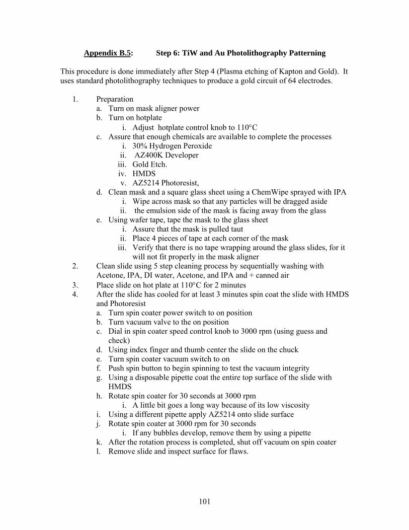
101
Appendix B.5: Step 6: TiW and Au Photolithography Patterning This procedure is done immediately after Step 4 (Plasma etching of Kapton and Gold). It uses standard photolithography techniques to produce a gold circuit of 64 electrodes.
1. Preparation a. Turn on mask aligner power b. Turn on hotplate
i. Adjust hotplate control knob to 110°C c. Assure that enough chemicals are available to complete the processes
i. 30% Hydrogen Peroxide ii. AZ400K Developer
iii. Gold Etch. iv. HMDS v. AZ5214 Photoresist,
d. Clean mask and a square glass sheet using a ChemWipe sprayed with IPA i. Wipe across mask so that any particles will be dragged aside
ii. the emulsion side of the mask is facing away from the glass e. Using wafer tape, tape the mask to the glass sheet
i. Assure that the mask is pulled taut ii. Place 4 pieces of tape at each corner of the mask
iii. Verify that there is no tape wrapping around the glass slides, for it will not fit properly in the mask aligner
2. Clean slide using 5 step cleaning process by sequentially washing with Acetone, IPA, DI water, Acetone, and IPA and + canned air
3. Place slide on hot plate at 110°C for 2 minutes 4. After the slide has cooled for at least 3 minutes spin coat the slide with HMDS
and Photoresist a. Turn spin coater power switch to on position b. Turn vacuum valve to the on position c. Dial in spin coater speed control knob to 3000 rpm (using guess and
check) d. Using index finger and thumb center the slide on the chuck e. Turn spin coater vacuum switch to on f. Push spin button to begin spinning to test the vacuum integrity g. Using a disposable pipette coat the entire top surface of the slide with
HMDS h. Rotate spin coater for 30 seconds at 3000 rpm
i. A little bit goes a long way because of its low viscosity i. Using a different pipette apply AZ5214 onto slide surface j. Rotate spin coater at 3000 rpm for 30 seconds
i. If any bubbles develop, remove them by using a pipette k. After the rotation process is completed, shut off vacuum on spin coater l. Remove slide and inspect surface for flaws.

102
m. If surface flaws are observed in the photoresist, then remove photoresist coating by spraying the slide with acetone, and then repeat step 5 process above
5. Soft bake the photoresist on hotplate for 2 minutes at 110°C 6. Expose slide to ultraviolet light.
a. Place mask and glass plate combination in mask aligner with the mask facing down, so you can read the writing through the glass
b. Place the slide below the mask and adjust using hand or wafer grabbers aligning the electrode pattern on the mask in the center of the slide
c. Note: if there is a flaw or a potential flaw in the Kapton or the gold that can be avoided, then align the mask so that the mask is not in near the flaw
d. Bring the slide in contact with the glass sheet using the z-axis micromanipulator or the chuck release
e. Visually assure that the mask is still aligned it the center of the slide and all of the electrodes will be in a place where it can be developed
f. Expose the surface to ultraviolet light for 27 seconds by pressing the expose button
g. Pull the slide out of the mask aligner and separate from the mask. 7. Prepare chemicals for patterning gold
a. Pour 25 ml of 4 : 1 (DI water : developer) solution of AZ400K developer into a container for each array that will be processed.
b. Pour 5mm to 10mm of gold etch into a container c. Pour 5mm to 10mm of hydrogen peroxide into container
8. Develop the photoresist a. Submerge and agitate the slide in the AZ400K developer for 60 seconds b. Remove with wafer grabbers c. Rinse with DI water d. Dry with canned air e. Inspect the photoresist layer using microscope
i. If shorts or breaks are visibly noticeable in the photoresist layer, then redo steps 2 threw 7
9. Etching the gold a. Submerge and agitate the slide in the gold etch for 90 seconds +/- 45
seconds i. When all the gold is removed from the etched areas, then remove
the slide and inspect. To identify if the gold is remove, lightly scratch the gold off an unimportant area of the slide with the wafer grabbers look for a contrast between the gold to no gold coverage. The gold is finished etching when there is no difference in appearance between the two areas. This trial and error approach will provide guidance for processing of subsequent arrays.
b. Remove with wafer grabbers c. Rinse with DI water d. Dry with canned air

103
e. NOTE: the gold etchant can be used for several arrays before it needs to be replace. It should be replaced when the etching time exceeds 150 seconds.
10. Remove Titanium-Tungsten a. Submerge and agitate the slide in the hydrogen peroxide for 40 seconds b. Remove with wafer grabbers c. Rinse with DI water d. Dry with canned air
11. Rinse slide with 5 step process a. Dry with canned air
12. Bake on hotplate for 3 minutes at 120 C 13. The gold patterning is now complete 14. Clean up
a. Dispose of all chemicals in there respective waste containers. b. Dispose of all pipettes and dirty ChemWipes from the fume hood in the
photoresist waste container c. Dispose of all dirty ChemWipes into waste receptacle in gowning room d. Assure that all vacuum lines, DI water pump, and spincoaters are turned
off.
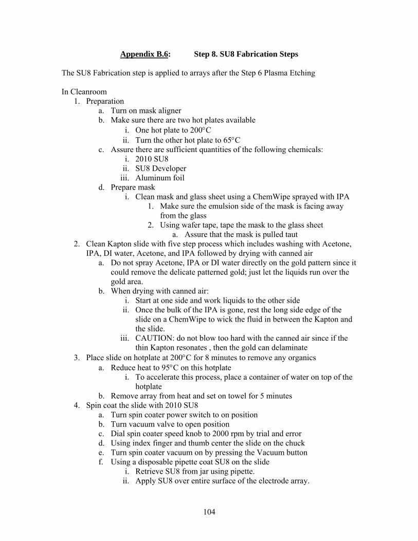
104
Appendix B.6: Step 8. SU8 Fabrication Steps
The SU8 Fabrication step is applied to arrays after the Step 6 Plasma Etching In Cleanroom
1. Preparation a. Turn on mask aligner b. Make sure there are two hot plates available
i. One hot plate to 200°C ii. Turn the other hot plate to 65°C
c. Assure there are sufficient quantities of the following chemicals: i. 2010 SU8
ii. SU8 Developer iii. Aluminum foil
d. Prepare mask i. Clean mask and glass sheet using a ChemWipe sprayed with IPA
1. Make sure the emulsion side of the mask is facing away from the glass
2. Using wafer tape, tape the mask to the glass sheet a. Assure that the mask is pulled taut
2. Clean Kapton slide with five step process which includes washing with Acetone, IPA, DI water, Acetone, and IPA followed by drying with canned air
a. Do not spray Acetone, IPA or DI water directly on the gold pattern since it could remove the delicate patterned gold; just let the liquids run over the gold area.
b. When drying with canned air: i. Start at one side and work liquids to the other side
ii. Once the bulk of the IPA is gone, rest the long side edge of the slide on a ChemWipe to wick the fluid in between the Kapton and the slide.
iii. CAUTION: do not blow too hard with the canned air since if the thin Kapton resonates , then the gold can delaminate
3. Place slide on hotplate at 200°C for 8 minutes to remove any organics a. Reduce heat to 95°C on this hotplate
i. To accelerate this process, place a container of water on top of the hotplate
b. Remove array from heat and set on towel for 5 minutes 4. Spin coat the slide with 2010 SU8
a. Turn spin coater power switch to on position b. Turn vacuum valve to open position c. Dial spin coater speed knob to 2000 rpm by trial and error d. Using index finger and thumb center the slide on the chuck e. Turn spin coater vacuum on by pressing the Vacuum button f. Using a disposable pipette coat SU8 on the slide
i. Retrieve SU8 from jar using pipette. ii. Apply SU8 over entire surface of the electrode array.

105
iii. If any bubbles appear use the pipette to suck them off. iv. Do not stick pipette into the SU8 to blow air out of the pipette.
This will inject the SU8 with bubbles and cause pits in future SU8 runs
g. Run spin coater at 2000 rpm for 30 seconds for a 10 μm thickness h. Turn off vacuum on spin coater and remove slide
5. Assure that the hotplate that was previously at 200 °C is now at 95°C 6. Place slide on first hot plate and soft bake the slide at 65 °C for 2 minute and
immediately following 95 °C for 3 minutes (on second hot plate) a. Assure before baking that both temperatures have reached the correct
temperature 7. Expose slide to ultraviolet light. (Although we have two electrodes on the slide,
we only develop one at a time) a. Place mask and glass combination in mask aligner with the mask facing
down b. Place the slide below the mask and adjust using wafer grabbers aligning
the two target marks on the mask to the one on the gold pattern c. Adjust using visual observations the alignment of the slides to the mask
i. Precise alignment during this step will reduce the difficulty in following steps.
ii. Align the top of one of the electrodes gold lines parallel to the top of the SU8 line using micromanipulators
iii. Using micromanipulators and microscope align the electrodes on the electrode arrays. If the electrodes are aligned then the electrode pads will also be aligned.
d. Bring the slide in contact with the glass sheet using the z-axis micromanipulator
e. As the slide is raised closer to the mask, recheck in the microscope that the mask is still aligned on the slide
f. Visually assure that the mask is still aligned it the center of the slide and all of the electrode will be in a place where it can be developed
g. Using the ultraviolet light, expose for 42 seconds 8. Post exposure bake consists of 3 minutes at 65 °C on the first hot plate followed
immediately by 5 minutes at 95 °C on the second hot plate. 9. Place slide on clean ambient surface and let cool for 5 minutes after baking 10. Develop SU8 on slide underneath the fume hood
a. Fill a container with 2010 SU8 Developer (about ¼ inch deep) b. Immerse the slide in Developer for 3 minutes with strong agitation
i. Make sure to change agitation directions from swirl clockwise and counter clockwise and up and down
c. Remove from developer with wafer grabbers d. Rinse with IPA followed by canned air drying e. Spray IPA directly on electrodes but on pad side by just letting the fluid
flow over it f. Dry with canned air
11. Cure on hotplate at 200 °C for 8 minutes

106
12. Inspect with microscope 13. The SU8 portion and all the cleanroom steps are now finished.
SU-8 Trouble Shooting If there is cracking in the SU8 coating:
1. It is likely an exposure time issue. This may be resolved by increasing the exposure time first or alternatively by reducing the exposure time.
2. If cracking continues to occur, adjust the pre-exposure and post-exposure bake times by trial and error.
3. If cracking continues assure the shelf life of the SU8 has not exceeded..

107
Appendix B.7: Step 9. Drill Alignment Holes This step puts holes into the Kapton so that it can be aligned to a circuit board in future steps
1. Remove an electrode array from the slide a. Using a razor blade cut the Kapton diagonally to separate the two different
electrodes from each other b. Remove tape from Kapton film
2. Fabricate drilling tool a. Acquire a 65mm to 40mm length of 1/8 inch diameter dowel pin b. Using a grinder, chamfer one end to between a 45 and 65 degree angle to
make a sharp point on one end c. Lightly grind a shallow and small chamfer on the back side of the point as
in Figure B.7.1 below
Figure B.7.1: Drilling Tool Grinding Schematic
i. The small chamfer will form a hole that is cut in the Kapton which is smaller than 1/8 inch, so that during assembly a press fit will be provided.
3. Gather materials: a. The alignment jig b. Tape

108
c. A single electrode that has gone through gold patterning and SU8 patterning.
d. Drilling tool 4. Aligning electrode in alignment jig
a. Place electrode over alignment jig putting the two targets of the electrode array over the corresponding holes in the jig
b. Cut off the parts of the Kapton film that lie over the screw holes or the alignment pin holes
c. Put tape on the left and right side of the electrode array d. Tape the electrode to the underside of the top half of the jig in the general
area e. Adjust the tape by doing one side and then the other until the holes and the
targets appear concentric 5. Place the bottom half of the alignment jig onto the top half aligning the alignment
pins 6. Place the two bolt into the bolt holes and tighten down until snug 7. Drilling the holes
a. Tighten the fabricated drilling tool into a drill press chuck b. Set spindle speed to about 400 rpm c. Lower the drilling tool tip 1/8 inch into the alignment jig, so that the
drilling tool is in the hole, but not touching the Kapton d. Turn on spindle e. Slowly lower the spindle so that the Kapton is cut all the way through f. Take the spindle up and down through the Kapton a few times to clean up
the edges and to make sure that it is cut all the way through 8. Removal of the electrode
a. Unscrew the bolts b. Remove the top half of the aligning jig c. Remove the tape
9. Inspect holes for no major tears 10. The drilling of the electrode is complete

109
Appendix B.8: Step 10-Constructing an Electrode Array This step assembles the microfabricated electrode array, zebra connector and circuit board with an alignment clamp.
1. Gather all components: a. Drilled electrode array b. Zebra interconnect strip
i. Cut Zebra strip into a length between 1 inch and 8/10 inch c. Circuit board d. Aligning clamp
2. Remove bolts from aligning clamp and remove the top acrylic part of the clamp 3. Put the electrode array onto the alignment pins
a. Place the alignment pins up on the aluminum part of the clamp b. Place the electrode array on top of the clamp, putting the drilled holes
directly over the alignment pins c. Hold the electrode array with one hand and use tweezers in the other to
gently force the Kapton over one pin i. Only press the Kapton down so that it just fits over the pin
d. Do the same for the other alignment pin e. Work the Kapton down on the alignment pin in steps. Push one side down
a small distance and then the other, back and forth until the Kapton is flush against the aluminum
f. If electrode array will not lie flat, apply tape to the edges of the array to make it taut.
4. Put the Zebra strip between alignment pins a. Place the zebra strip over the center part of the electrode array connection
pads b. Make sure that the zebra strip is parallel with ends of the connection pads
5. Put circuit board on alignment pins a. Place the circuit board on top the zebra connector b. Assure the black pin connectors are facing up c. Assure the circuit board is facing the opposite way of the electrode array,
so that it is not covering the electrode array up 6. Clamp the circuit board, zebra strip and electrode array together
a. Place the acrylic cover on top of the circuit board b. Press firmly down on the acrylic piece with one hand c. With the other hand tighten down the bolts on each side of the electrode. d. Ensure that the acrylic is even and that the zebra connector is similar to the
that shown in Figure B.8.1

110
Figure B.8.1: Side Pictorial of the Proper Squish for the Zebra Connector

111
Appendix B.9: Step 11- Cutting Electrode Array into Final Form This step cuts the Kapton part of the electrode array so that it may be implanted in a subject.
1. Preparation a. Electrode Array from Step 10 with interconnect attached b. a razor blade and c. tape
2. Tape the right and left edges half way up the electrode onto an elevated piece of about ~¼ inch thick cutting plate (either aluminum or plastic) so that the array can set level with the connector lying on the bench top. The taped flat electrode array should have the basic shape shown below in Figure: B.11.1.
Figure B.11.1: Electrode Array Before Cutting
3. Using the razor blade cut the Kapton film in a arc as shown below in order to round of the bottom edge as shown in Figure B.11.2.
Figure B.11.2: Rounding Cut on Electrode Array
4. Using the razor blade cut the Kapton film as shown in figure B.11.3 so that the areas adjacent to the array can be removed up to the top of the electrodes.

112
Figure B.11.3: Finished Cut on Electrode Array
5. The electrode array is finished and ready for implantation.

113
Appendix C.1: Preparation of Saline Solution
1. Material and Equipment a. A scale that is accurate to at least 0.01 grams b. Table salt c. DI water d. 100 to 500 mL Nalgene bottle with top
2. Add salt a. Place the Nalgene bottle on scale b. Zero the scale c. Add 0.9 grams of salt
3. Add DI water a. Zero the scale b. Using disposable pipette, add in 99.1 grams DI water
4. Shake the solution until all no salt particles are visible in the solution 5. Label the saline solution which can be used for multiple arrays until it is
consumed. 6. The saline solution is done
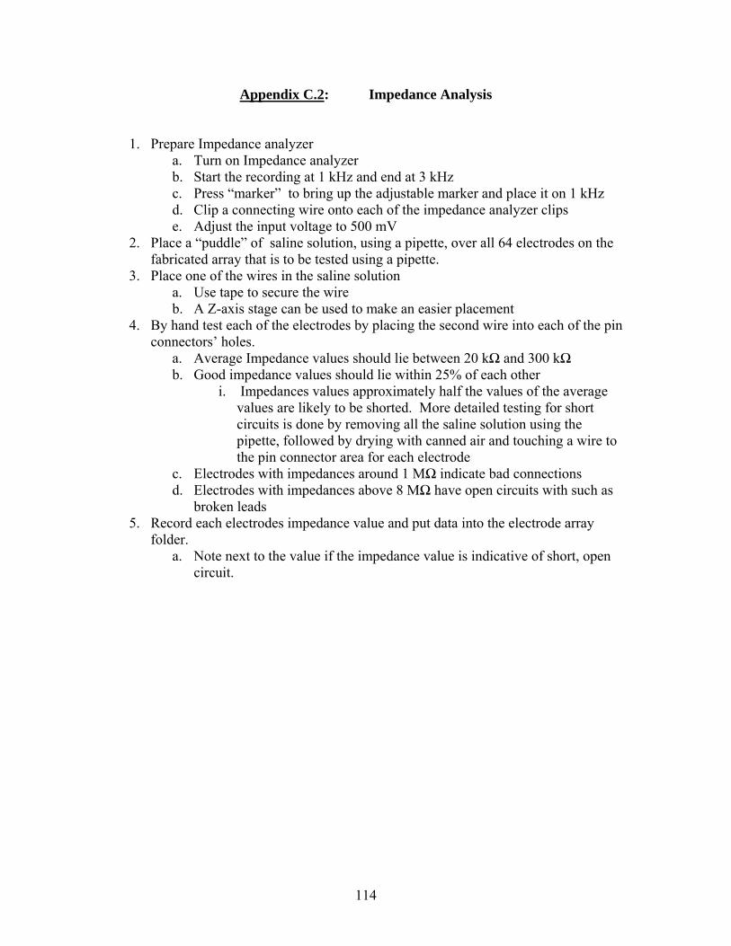
114
Appendix C.2: Impedance Analysis
1. Prepare Impedance analyzer a. Turn on Impedance analyzer b. Start the recording at 1 kHz and end at 3 kHz c. Press “marker” to bring up the adjustable marker and place it on 1 kHz d. Clip a connecting wire onto each of the impedance analyzer clips e. Adjust the input voltage to 500 mV
2. Place a “puddle” of saline solution, using a pipette, over all 64 electrodes on the fabricated array that is to be tested using a pipette.
3. Place one of the wires in the saline solution a. Use tape to secure the wire b. A Z-axis stage can be used to make an easier placement
4. By hand test each of the electrodes by placing the second wire into each of the pin connectors’ holes.
a. Average Impedance values should lie between 20 kΩ and 300 kΩ b. Good impedance values should lie within 25% of each other
i. Impedances values approximately half the values of the average values are likely to be shorted. More detailed testing for short circuits is done by removing all the saline solution using the pipette, followed by drying with canned air and touching a wire to the pin connector area for each electrode
c. Electrodes with impedances around 1 MΩ indicate bad connections d. Electrodes with impedances above 8 MΩ have open circuits with such as
broken leads 5. Record each electrodes impedance value and put data into the electrode array
folder. a. Note next to the value if the impedance value is indicative of short, open
circuit.

115
Appendix D: Impedance Maps
Electrode X11 A B C D E F G H 1 19 24 12 11 23 25 9 8 2 17 30 22 11 22 24 8 8 3 11 19 25 24 22 26 23 8 4 10 19 25 21 25 24 26 28 5 18 19 23 24 22 24 43 14 6 20 19 19 21 18 22 50 14 7 17 22 24 21 23 22 26 25 8 21 23 26 20 13 21 18 27 Unit: kohms Impedance tested at 500mV input voltage for Electrode X2-X11 Electrode X10 A B C D E F G H 1 16 42 14 30 16 32 9 10000 2 15 19 16 10000 13 8000 12 12000 3 17 16 15 16 9000 18 16 17 4 16 16 16 10000 14 16 16 17 5 9000 17 16 14 18 13 10000 14 6 25 16 16000 10000 10000 12 17 13 7 27 16 12000 16 20 14 10 12 8 13000 12000 32 15 12000 15 10 14 Unit: kohms Electrode X9 A B C D E F G H 1 29 20 72000 25 32 31 23 34 2 25 19 19 22 23 22 13000 27 3 23 23 21 19 28 76 26 33 4 21 22 21 24 24 22 21 29 5 20 22 19 22 20 20 32 32 6 20 19 20 21 19 22 31 27 7 18 20 20 20 20 19 20 22 8 19 16 17 19 33 21 22 13000 Unit: kohms Electrode X8 A B C D E F G H 1 20 13000 20 13000 23 14000 25 37 2 19 22 22 20 22 14000 23 13000 3 19 22 20 22 27 78 22 28 4 16 18 16 23 25 22 20 28 5 21 18 17 19 25 21 24 14000 6 22 19 22 22 25 20 23 21 7 25 19 20 22 13000 23 15000 25 8 20 20 32 19 15000 21 14000 27 Unit: kohms

116
Electrode X7 A B C D E F G H 1 22 32 23 78 25 20000 23 20000 2 34 17000 22 35 17 20 24 20000 3 29 30 26 17000 18 27000 22 20000 4 20000 22 24 24 13 26 22 20000 5 24 20 28 290 28 22 21 20000 6 27 22 50 20000 29 30 20000 20000 7 20000 22 17000 23 20000 22 20000 20000 8 20000 20 37 20000 20000 31 20000 20000 Unit: kohms Electrode X6 A B C D E F G H 1 23 29 22 22 19 103 19 8000 2 24 22 24 21 8000 94 21 28 3 280 351 27 25 21 8000 18 8000 4 24 245 32 18 21 18 20 17 5 10000 216 34 12 20 17 18 18 6 940 204 3000 12 8000 19 8000 18 7 68 33 22 21 24 10000 7000 22 8 65 9000 20 25 12 10000 13000 24 Unit: kohms Electrode X5 A B C D E F G H 1 33 30 32 27 34 28 36 18000 2 25 24 23 18000 25 28 23 29 3 26 19 25 25 25 160 23 29 4 26 24 26 27 16 44 32 28 5 25 25 24 26 17 32 32 60 6 23 26 16 25 26 26 20000 24 7 26 24 20 24 30 24 30 42 8 28 36 21 33 31 34 32 28 Unit: kohms Electrode X4 A B C D E F G H 1 37 32 33 28 36 33 36 16000 2 25 25 24 17000 27 32 27 38 3 27 18 26 26 27 176 28 35 4 25 24 28 28 17 45 40 30 5 24 25 25 26 16 34 41 60 6 22 25 13000 27 29 31 18 30 7 28 25 19000 28 33 30 37 50 8 28 38 20000 35 33 36 37 23000 Unit: kohms

117
Electrode X3 A B C D E F G H 1 47 34 34 30 43 29 38 18 2 43 31 28 24 28 28 26 9000 3 27 14 25 23 24 28 8000 27 4 26 14 26 16 25 24 47 32 5 23 13 27 12000 24 28 27 23 6 28 12 10000 28 32 180 21 25 7 25 32 27 29 28 148 19 24 8 28 37 33 47 31 40 29 32 Unit: kohms Electrode X2 A B C D E F G H 1 198 97 108 85 100 71 109 19000 2 72 77 68 16000 67 77 66 74 3 78 18000 66 72 64 64 64 74 4 74 86 84 79 38 71 68 73 5 115 82 75 74 36 199 70 71 6 92 80 11000 67 67 66 19000 67 7 105 73 16000 68 78 68 85 73 8 278 100 15000 96 88 98 81 19000 Unit: kohms Electrode X1 A B C D E F G H 1 300 393 291 251 260 136 79 157 2 259 294 215 189 205 187 81 185 3 245 272 182 181 175 275 149 161 4 209 279 201 186 179 184 180 172 5 266 266 219 225 199 240 229 195 6 16000 249 194 257 283 233 222 251 7 288 277 217 234 206 242 253 260 8 226 241 191 227 252 273 257 254 Unit: kohms Impedance tested at 50mV input voltage for Electrode X1