Embed Size (px)
Citation preview

A METHOD FOR CHARACTERIZATION OF SINGLE-EVENT LATCHUP IN CMOS
TECHNOLOGIES AS A FUNCTION
OF GEOMETRIC VARIATION
By
Matthew Joplin
T. Daniel Loveless
UC Foundation Assistant Professor of Electrical Engineering
(Chair)
Abdul R. Ofoli
UC Foundation Associate Professor of Electrical Engineering
(Committee Member)

ii
A METHOD FOR CHARACTERIZATION OF SINGLE-EVENT LATCHUP
IN CMOS TECHNOLOGIES AS A FUNCTION
OF GEOMETRIC VARIATION
By
Matthew Joplin
A Thesis Submitted to the Faculty of the University of
Tennessee at Chattanooga in Partial
Fulfillment of the Requirements of the Degree
of Master of Engineering
The University of Tennessee at Chattanooga
Chattanooga, Tennessee
August 2018

iii
ABSTRACT
Complementary metal-oxide-semiconductor (CMOS) technology is the dominant
integrated circuit (IC) technology in modern electronics systems. As CMOS comprises of p-
channel and n-channel transistors, there are parasitic PNPN paths that act as cross-coupled bipolar
transistors capable of creating low-impedance paths between the power supply rails known as the
“latchup” state. Latchup is destructive and requires a power cycle to restore operation. Latchup
can be stimulated by ionizing radiation such as a high-energy proton or heavy-ions from deep
space, resulting in a significant vulnerability in CMOS space systems. The sensitivity of an IC to
single-event latchup (SEL) depends on various process parameters as well as design geometry.
This work presents a method for the characterization of the geometric effects of CMOS layout on
SEL. The dominant geometric contributors to the overall SEL sensitivity include: (1) substrate
contact-to-source spacing (PWNS), (2) well contact-to-source spacing (NWPS), and (3) source-
to-source spacing (SS).

iv
DEDICATION
I dedicate this work to the incredible people in my life who have tirelessly encouraged me,
inspired me, and helped me throughout my unorthodox education: my friends, my family, and my
teachers. My sincerest gratitude is owed to them, and I would not be who I am without them.

v
ACKNOWLEDGMENTS
I acknowledge my committee: Dr. Daniel Loveless and Dr. Abdul Ofoli, and I thank them
for taking the time and effort to evaluate the quality of this research. This work was supported in
part by the Tennessee Higher Education Commission (THEC) through the Center of Excellence in
Applied Computational Science and Engineering (CEACSE) Program at the University of
Tennessee at Chattanooga.

vi
TABLE OF CONTENTS
ABSTRACT ....................................................................................................................... iii
DEDICATION ................................................................................................................... iv
ACKNOWLEDGMENTS ...................................................................................................v
LIST OF TABLES ........................................................................................................... viii
LIST OF FIGURES ........................................................................................................... ix
LIST OF ABBREVIATIONS ............................................................................................ xi
LIST OF SYMBOLS ....................................................................................................... xiii
CHAPTER
I. INTRODUCTION ................................................................................................1
II. BACKGROUND ..................................................................................................3
Space Environment ...............................................................................................3
Electronic CMOS ..................................................................................................7
Single Event Effects ..............................................................................................8
Single Event Latchup ............................................................................................9
Mitigation Techniques and SAFE Space ............................................................18
III. INFLUENCE OF GEOMETRY ON SEL SENSITIVITY ................................22
Introduction .........................................................................................................22
Description of Latchup Stages ............................................................................27
Parasitic BJT and Resistor Model .......................................................................29
Geometric Effect Trends on Latchup Sensitivity................................................32
Translating Physical Spacing to Model Resistance ............................................35

vii
LTSPICE Simulation ..........................................................................................37
SEL vs. Geometric Variation Characterization Test Variants ............................40
Conclusion ..........................................................................................................44
IV. TEST CHIP DESIGN FOR PARAMETRIC ANALYSIS OF SEL ..................45
Introduction .........................................................................................................45
PNPN Layout ......................................................................................................48
Electrical Latchup Considerations ......................................................................51
Single-Event Latchup Testing Considerations ....................................................54
Conclusions .........................................................................................................57
V. DISCUSSION .....................................................................................................58
VI. CONCLUSIONS ................................................................................................60
VII. SIGNIFICANCE .................................................................................................61
REFERENCES ..................................................................................................................62
VITA ..................................................................................................................................64

viii
LIST OF TABLES
1 List of Test Samples Needed for Geometric Characterization ............................................... 35
2 Implemented Geometric Variant Test Set ............................................................................... 47
3 Test Chip Connectivity Matrix ............................................................................................... 47

ix
LIST OF FIGURES
1 Near-earth space radiation environment, after K. Endo ........................................................... 4
2 South Atlantic Anomaly in blue, after ESA.............................................................................. 5
3 Relative abundance and flux density of particles vs. atomic Z number ................................... 6
4 Diffusion cross-section of CMOS inverter well structure and inverter circuit diagram ........... 7
5 Single event transient time diagram and the resulting single event transient current, after
Massengill ........................................................................................................................... 9
6 Intrinsic parasitic BJTs within CMOS well structure ............................................................. 10
7 Illustration of parasitic bipolar positive feedback loop........................................................... 11
8 Latchup behavioral circuit model, after Artola ....................................................................... 13
9 Common-emitter gain product of parasitic BJTs from 180 nm to 65nm, after Boselli .......... 15
10 PNPN latchup test structure top-down layout, after IEEE Electron Devices Society .......... 17
11 Example PNPN guard ring top-down layout ........................................................................ 18
12 Common-base gain resistance SAFE space, after Troutman ................................................ 20
13 Annotated diagram of the PNPN SEL test structure showing terminal names, values, and
linear dimensions .............................................................................................................. 23
14 Differential two-photon absorption sensitivity map of PNPN structure, after Dodds .......... 26
15 Four stages of triggering latchup with currents in red, after Artola...................................... 28
16 180 nm TCAD extracted resistance values for the PNPN circuit model, after Youssef ...... 30
17 Calculated and measured SET waveform and collected charge of a 15 MeVcm-2mg-1
SE, after Artola ................................................................................................................. 32
18 Source-to-source spacing (left) and well-to-source spacing (right) vs. trigger current (red)
and holding current (black), after Artola .......................................................................... 33

x
19 Coupling resistance, RCW, sweep (left) and trigger resistance, RBS, sweep (right) latchup
response............................................................................................................................. 39
20 Physical dimension radar maps showing the independent variation of geometric
parameters ......................................................................................................................... 41
21 Example Qcrit vs. geometry contour plot ............................................................................. 43
22 Diagram of a sample test block with electrical latchup and single event latchup modes ..... 46
23 Diagram of low (top) and high (bottom) substrate contact (SC) densities ........................... 51
24 I-Test circuit diagram, from JESD78 .................................................................................... 53
25 Overvoltage test circuit diagram, from JESD78 ................................................................... 54
26 Sensitive area of a laser latchup structure, after Artola ........................................................ 56

xi
LIST OF ABBREVIATIONS
ADDICT, Advanced Dynamic DIffusion Collection Transient model
BJT, bipolar junction transistor
CME, coronal mass ejection
CMOS, complementary metal-oxide-silicon
ESA, European Space Agency
GCR, galactic cosmic ray
GR, guard ring
IC, integrated circuit
IEEE, Institute of Electrical and Electronics Engineers
LBNL, Lawrence Berkeley National Lab
LEO, low-Earth orbit
LET, linear energy transfer
NS, n-type source
NW, n-well contact
NWPS, n-well-to-p-source spacing geometry parameter
PNPN, latchup path or latchup test structure
PS, p-type source
PW, p-substrate contact
PWNS, p-well-to-n-source spacing geometry parameter

xii
SAA, South Atlantic Anomaly
SC, substrate contact
SCR, silicon-controlled rectifier
SE, single event
SEE, single event effect
SEL, single event latchup
SS, source-to-source spacing geometry parameter
TAMU, Texas A&M University Cyclotron Institute
UNOOSA, United Nations Office for Outer Space Affairs

xiii
LIST OF SYMBOLS
GND, system ground
IHold, holding current or corresponding current to sustain latchup
ITrig, trigger current or corresponding current to trigger latchup
VDD, system operating supply voltage
VHold, holding voltage or maximum current to sustain latchup
VTrig, trigger voltage or minimum voltage to trigger latchup
XSS, source-to-source dimension
XPWNS, p-well-to-n-source dimension
XNWPS, n-well-to-p-source dimension
αn, lateral parasitic NPN common-base gain
αp, vertical parasitic PNP common-base gain
βn, lateral parasitic NPN common-emitter gain
βp, vertical parasitic PNP common-emitter gain

1
CHAPTER I
INTRODUCTION
The United Nations Office for Outer Space Affairs (UNOOSA) maintains the Index of
Objects Launched into Outer Space, and it lists approximately 4,800 human-made satellites in orbit
around Earth with more than 8,100 total satellites launched since Sputnik 1 in 1957 [1]. They
transmit and receive telecommunication, television, and GPS signals to provide commercial
services and collected data from scientific missions carried out by many international space
programs. Satellites have enabled modern discoveries and technologies.
However, the space environment is not as empty as it appears to be; radiation from the sun
and galactic cosmic rays (GCRs) make up a highly dynamic radiation environment. Charged
particles and electromagnetic rays over a spectrum of energy and mass are plentiful enough that
they interact with satellite electronics and have observable effects (known as single event effects
or SEEs) on electrical system operation. Among the most destructive SEEs is single event latchup
(SEL) or particle-induced latchup.
The latchup phenomenon occurs in Complimentary Metal-Oxide-Silicon (CMOS) when a
low-impedance stable state forms between the power rails. The phenomenon is enabled by the
interplay of parasitic bipolar junction transistors (BJTs) formed by the CMOS well structure and
caused by minority charge carriers injected into the body terminals of the parasitic BJTs. Various
parameters impact the behavior of latchup including environment, operating voltage, silicon
doping profile, and geometric layout.

2
The purpose of this work is to generate meaningful feedback to CMOS integrated circuit
designers who have control over the geometry of the electronic devices such that they may make
informed design decisions to predict and mitigate single event latchup in their designs before
manufacturing.
This work quantifies the effect of changing parameters that are under the control of a
CMOS circuit designer such as physical layout dimensions like well contact-to-source spacing and
PMOS to NMOS source spacing. Moreover, this work compares changing physical dimensions
directly to standard latchup-hardening techniques. The general trends of geometry upon latchup is
well-documented in the literature, but it is important to realize that latchup behavior is unique for
each CMOS process and therefore the effect must be uniquely characterized for each process. This
work provides such a method for geometric characterization of SEL with geometrically-varied
devices, an outline of radiation test considerations, an experimental test design, a definition of a
latchup behavioral model dependent on measured device parameters, and the analytical simulation
results and parameters.

3
CHAPTER II
BACKGROUND
Space Environment
The space environment consists of charged particles that have a wide range of mass,
energy, and velocity. The ionizing particles interact with the environment around them and the
materials they pass through via Rutherford scattering [2]. The Sun is a significant contributor to
the dynamic radiation environment, especially in the case of coronal mass ejections (CME), which
mainly consist of high-energy electrons and protons, eager to interact with the first reactive
materials they encounter. On Earth, CMEs can even cause power outages, communications
blackouts, and send the aurora stretching toward the equator as it did during the “Carrington Event”
in 1859. Fortunately, there was not much power and communications infrastructure back then.
Figure 1 [3] shows an illustration of the dynamic radiation environment around Earth caused by
the Sun and the Earth’s magnetic field.

4
Figure 1
Near-earth space radiation environment, after K. Endo [3]
The magnetic field shields the Earth from most high energy particles, but some can still get
through to low altitude. Charged particles can get trapped within the magnetic field lines and where
the magnetic field lines converge is the South Atlantic Anomaly displayed in Figure 2 [4]. The
South Atlantic Anomaly is a spot of the low-strength magnetic field shown in blue.

5
Figure 2
South Atlantic Anomaly in blue, after ESA [4]
There is an appreciable drop in the magnetic field intensity of Earth over South America due to
the inclination of the magnetic poles, which allows high-energy particles to penetrate to lower
altitudes and consequently interact with satellite electronics in lower orbits.
There is still more to the space radiation environment outside of the magnetosphere. For
example, Galactic Cosmic Rays (GCRs), made up of the highest energy ions from deep space,
originate outside of the solar system. These particles can cause the most destructive effects such
as SEL due to their greater atomic mass and energy. However, because they originate from such a
long distance away, they are relatively uncommon when compared to solar radiation as shown by
the chart in Figure 3 [2].

6
Figure 3
Relative abundance and flux density of particles vs. atomic Z number [2]
Figure 3 shows that the relative abundance of heavy-ions with Z >2 is between 100 and 2000 times
less abundant than solar protons. These heavy-ions are the main contributor to single event latchup
(SEL) events in satellite electronics.

7
Electronic CMOS
Complimentary Metal-Oxide-Silicon (CMOS) processes are used to make digital
electronic devices. In the context of electronics, bulk planar CMOS is especially susceptible to
radiation. This susceptibility is due to the inherent metastability of CMOS. The crux of CMOS is
its switching between two possible output states. The deliberate placement of n-type diffusions
placed in a p-type substrate (or p-type diffusions placed in an n-type substrate) to form CMOS
devices as shown in Figure 4 accomplish this metastable behavior.
There are neutrally charged depletion regions between n-type and p-type charge
concentrations. The sizes of the depletion regions depend upon the diffusion of minority charge
carriers and doping around the p-n junctions. The depletion regions separate positive and negative
charge bubbles maintained by built-in voltages at equilibrium. Radiation, however, can upset this
equilibrium.
Figure 4
Diffusion cross-section of CMOS inverter well structure and inverter circuit diagram

8
Because CMOS takes advantage of complementary PMOS and NMOS devices, there are
intrinsic parasitic bipolar junction transistors (BJTs) within the well-substrate structure. Most of
the time, these BJTs do not conduct, because there is not sufficient emitter-base voltage to forward-
bias the devices in the first place. Nominally, the CMOS device channels bypass the BJTs and
there is no interference with operation.
Single Event Effects
When a single ionizing particle interacts with semiconductors in electronics, this is called
a Single Event (SE). For each SE, there is energy imparted to the device crystal lattice due to
Rutherford Scattering and this energy is defined as Linear Energy Transfer (LET). LET is
measured in MeV cm-2 mg-1 and is the energy lost by the particle as it travels through the lattice;
it is a linear function of the particle path length traveled through the device. The rule of thumb is
1pC per micrometer traveled through the substrate is equivalent to a LET of 100 MeV cm-2 mg-1
(in silicon). Figure 5 shows the process of deposited energy exciting electrons to the conduction
band, consequently inducing a low-impedance path by generating excess electron-hole pairs. A
transient current is observed as the electrons and holes are swept out by the applied electric field
and are collected at the drains of the NMOS and PMOS devices. [2]

9
Figure 5
Single event transient time diagram and the resulting single event transient current, after
Massengill [2]
SEEs are diverse, and range from correctable bit flips in combinational logic to destructive
current spikes that can take down entire subsystems. The latter effect is known as a single event
latchup (SEL), and it is the central focus of this work.
Single Event Latchup
SEE phenomena include Single Event Latchup (SEL), which is a subset of the well-
documented latchup phenomenon in CMOS structures. SEL is caused by high-LET particles that
forward-bias one of the parasitic BJTs. These particles can include protons as documented by ESA
in 1992, if the CMOS device is particularly sensitive to SEL such as an SRAM, but are usually
stimulated by heavy-ions from the deep space GCR spectrum [5].
Latchup is the creation of a low-impedance path between the power rails and is a persistent
effect that requires a power cycle to extinguish. The intrinsic PNPN path within the CMOS well

10
structure produces a pair of cross-coupled parasitic bipolar devices shown as Q1 and Q2 in Figure
6.
Figure 6
Intrinsic parasitic BJTs within CMOS well structure
The parasitic bipolar devices are usually off and do not affect nominal operation of the
CMOS circuit. However, when the parasitic devices are activated, the cross-coupled devices form
a positive feedback loop, as shown in Figure 7, that drives the parasitic bipolar devices into the
saturation region of operation, consequently producing a current spike and drop in operating
voltage. The feedback will sustain the latchup until the voltage supply is reduced below the
minimum holding voltage (VHold) threshold and the latchup is extinguished [6].

11
Figure 7
Illustration of parasitic bipolar positive feedback loop
The latchup structure is made up of the PNPN path formed by the nested well and diffusions
within the substrate. The two weak BJTs formed by this path share body/collector junctions.
Therefore, current that flows out from the collector junction of one BJT will feed into the body of
the other. The trigger stage in which the device affected by the SEL or injected current is in the
linear forward active mode and serves to drive the other device into saturation, which in turn drives
the origin device into saturation and the persistent latchup state.
The latchup criteria are as follows [6], [7], [8], [9]:
1. The product of the common-emitter gains (βp βn in Figure 7) of the combined BJT
structure must exceed unity to produce unstable positive feedback.
2. The triggered device must remain on long enough to drive the complementary
device into saturation.
3. The power source must be capable of supplying the holding current at the minimum
sustaining holding voltage.
Criterion (2) corresponds to reaching a minimum threshold point value (Vtrig, Itrig) that
initiates the latchup. The common-emitter gain criteria may be expressed in terms of the sum of

12
the common-base gains exceeding unity. Expressing the criterion in as the sum of common-base
gains exceeding unity is used by Troutman to plot the latchup sensitivity and SAFE space of the
PNPN structure. [9]
The latchup structure can be represented as a circuit behavioral model as shown in Figure
8 [8]. The model includes the junction resistance, the substrate resistance, the well resistance, and
two cross-coupled BJTs. This model relies on measured resistance and BJT characterization values
to accurately represent latchup behavior. However, even without the specific resistances, the
behavioral model is useful in exploring the effect of the resistor values on latchup behavior, which
is related to the spacing parameters under study in this work.

13
Figure 8
Latchup behavioral circuit model, after Artola [8]
Using the model in Figure 8 as a basis for simulating latchup behavior, the critical SEL
parameter values for VHold and VTrig are calculated from the following equations after Artola [8],
[10], [11]:
−−=
BS
EWPNPthDDTrig
R
RVVV 1 (1)
DDBWCWES
BWBS
ESEWEW
TrigHold VRRR
RR
RRR
VV++
−
−=
1
(2)

14
VTrig requires knowledge of the vertical parasitic BJT threshold voltage, VPNPth, well
emitter resistance, REW, and the substrate trigger resistance, RBS. VTrig represents the minimum
required voltage to forward-bias the vertical parasitic BJT. VHold represents the level above which
sustains the latchup phenomenon. It depends on VTrig and a combination of the resistors in the
model due to the feedback loop that sustains latchup behavior.
The resistors in the circuit model are sorted into three groups: trigger resistance (RBW and
RBS), coupling resistance (RCW and RCS), and emitter resistance (REW and RES). Trigger resistors
represent the substrate and well resistance and are dubbed “trigger” because if the values are not
above a certain threshold, then there will not be a sufficient voltage drop across the emitter-body
junction to forward-bias affected parasitic BJT. Coupling resistors set the strength of the coupling
between the devices, and define the maximum value of the latchup current. Emitter resistance
considers the type of contact (ohmic or resistive) that connects with the power rails.
The common-emitter gain (β) is a standard BJT parameter because it makes up one of the
three parameters for the Ebers-Moll BJT, and describes the ratio of collector current to body
current. In modern BJT devices, the forward common-emitter current gain, βF, can be on the order
of 102 or 103 when in linear mode of operation. Appropriate doping profiles and increasingly small
base widths produce these gain values. The following equation gives the intrinsic value of
common-emitter gain, β0, ignoring dependence on temperature and mode of operation:
𝛽0 =𝑁𝐸𝑚𝑖𝑡𝑡𝑒𝑟
𝑁𝐵𝑎𝑠𝑒𝑊𝐵𝑎𝑠𝑒 (3)
In the context of latchup, the base/collector junctions of the cross-coupled BJTs are the p-
substrate and the n-well, which are more diffuse than a modern BJT, and consequently, the

15
parasitic devices have significantly smaller common-emitter gains. However, the work of Boselli
et al. reveals that latchup is possible down to deep sub-micron nodes [12]:
Figure 9
The common-emitter gain product of parasitic BJTs from 180 nm to 65nm, after Boselli [12]
Figure 9 also shows that the parasitic BJTs do not have the significant gains seen in modern
commercial bipolar devices because the comparatively large well and substrate volume does not
act as an efficient base. The charge carriers are more likely to be lost to recombination and
exponentially dissipate as they approach the diffusion length.

16
However, as shown by Boselli, the parasitic structures are still able to meet the latchup
criteria:
𝛽𝑛 ∗ 𝛽𝑝 > 1 (4)
The result in Figure 9 signals that latchup, and therefore the SEL effect will continue to be a
challenge as modern integrated circuits continue to mature into these technology process nodes.
The simplest way to realize this behavioral model of latchup is with the PNPN test structure
for latchup shown in Figure 10 [13]. The PNPN test structure is most like the CMOS inverter, but
with a combined source and drain and no gate oxides within the structure. It reproduces the
parasitic bipolar structures within CMOS circuits and is meant to approximate the diffusion-well-
substrate structure used in an application.

17
Figure 10
PNPN latchup test structure top-down layout, after IEEE Electron Devices Society [13]
The PNPN structure is a four-terminal device and acts as a thyristor or silicon controlled
rectifier (SCR) [13]. The p-type substrate contains the n-type well, the n-type source (NS –
cathode), and the p-type well contact (PW – ground potential). The n-type well contains the p-type
source (PS – anode) and the n-type well contact (NW – VDD power source). The emitter terminals
of the parasitic BJTs are the anode and cathode. These are the primarily sensitive nodes of the
PNPN structure, and current injection into these nodes can induce electrical latchup.

18
Mitigation Techniques and SAFE Space
Even though a device may be susceptible to latchup, there are many methods available to
mitigate or “harden” the device to the unwanted effect. These techniques include spoiling
common-emitter gain with gold doping, neutron irradiation, dielectric trench isolation around the
CMOS well, SOI technology, triple-well structures, and use of an epitaxial layer on a low-
resistivity substrate [14]. Another method is decoupling the devices with a structure called a “guard
ring” (GR) as shown in Figure 11 below.
Figure 11
Example PNPN guard ring top-down layout

19
The GR acts as a “pre-collector” and serves to attract excess charge that may be generated
near the anode and cathode of the latchup structure (PS and NS of Figure 10) and shunt the current
transient to the appropriate power rail. The GR is a particularly useful hardening method if the
latchup-sensitive devices are known.
However, it is possible to manipulate the gain of the PNPN structure further without the
need for process-level variations or to sacrifice silicon area.

20
Figure 12
Common-base gain resistance SAFE space, after Troutman [9]
Troutman presented a latchup model in 1987 that defined the common-base gain “SAFE
space” based on the variation of the model’s resistance values. It is, therefore, possible to change
the effective gain of the parasitic structure using only its resistance, moreover, it is possible to
identify a threshold at which SEL becomes impossible altogether. What Figure 12 shows is the
required well resistance to control the common-base gain sum for a given substrate resistance.
With a mapped space like this, it is possible to add an external resistance network to ensure that
the system remains in the latchup-immune “SAFE space” [9]. The SAFE space is the area defined

21
by the vertices the triangle defined in Figure 12. The x-axis is the modified common-base gain
value, αn*, for the lateral parasitic BJT and the y-axis is the modified common-base gain value,
αp*, for the vertical parasitic BJT. They are both affected by the well resistance values RW and RS.
In the case of Figure 12, RS is held constant at 1000 Ω, and the numbered arrows represent the ITrig
transfer behavior to the latchup state (the hypotenuse of the triangle defines the latchup borderline)
for various values of RW.

22
CHAPTER III
INFLUENCE OF GEOMETRY ON SEL SENSITIVITY
Introduction
The susceptibility of electronics to radiation effects is difficult to quantify without
parameter characterization. An application may make it past many phases including design,
validation, fabrication, and reviews before exhibiting an unacceptable level of susceptibility to
destructive radiation effects during testing – one of the last phases of qualification before
production. The case of the National Semiconductor DS90C031 differential line driver as studied
by McMarrow at the Naval Research Laboratory [15] is a good example of this difficulty. The part
was thought to be space-qualified and its design was built into a new system, but it exhibited
unexpected SEL during heavy-ion testing and a redesign was required to prevent latchup.
Susceptibility to radiation effects can be mitigated or eliminated during the design stage,
but only if the mitigation techniques are understood and defined in the context of an application.
SEL is a destructive effect that can compromise entire systems, and therefore the effect must be
quantified for each application in radiation testing such as proton irradiation and heavy-ion
irradiation. Unfortunately, applying new technology in a radiation environment can lead to dubious
and undesirable results when put to the test as in [15], which is why it is so valuable to establish
an expected baseline response to radiation effects like SEL. To that end, this work defines a
methodology of characterizing SEL response as a function of geometric parameters under the

23
control of CMOS designers to produce accurate estimates of SEL susceptibility and to inform
geometric design changes prior to fabrication and radiation testing.
Characterizing geometric parameters will enable accurate SEL susceptibility estimations
given that transistor widths and lengths are known. Furthermore, the SEL characterization
methodology defined in this work can apply to other technologies, and it is applied here in
180 nm CMOS technology. This work studies the geometric parameters of device-to-rail spacing
parameters (PWNS and NWPS) and the device-to-device spacing parameter (SS). Figure 13 below
is an annotated version of the PNPN SEL test structure. The linear dimensions of the spacing
parameters (XPWNS, XNWPS, and XSS) will be varied to characterize the SEL sensitivity of the test
structure.
Figure 13
Annotated diagram of the PNPN SEL test structure showing terminal names, terminal values,
and linear dimensions

24
Perhaps the most important of the annotations is the length, L, which corresponds to the
gate length of the technology node – 180 nm in this case. Width, W, of the PNPN SEL test structure
is twenty times the length, as defined by [13] to linearize the SEL response into a one-dimensional
function of the geometric dimensions XPWNS, XNWPS, and XSS. The four terminal names are as
follows: NW for the N-well, PS for the P-source, NS for the N-source, and PW for the P-substrate.
Voltage values of the terminals that are denoted after the forward slash define the required voltages
to test the PNPN SEL test structure. VDD is the supply power voltage rail, GND is the ground
supply power rail, and Anode and Cathode are voltage variables used to excite the PNPN structure
into the latchup state as described in Chapter IV and in JESD 78 [17].
Individual transistor device dimensions are not affected by SS, NWPS, and PWNS because
affect the well-substrate structure shape. Therefore, the CMOS device response to biasing will not
change, but the parasitic BJT parameters will be affected by variation in device-to-rail and device-
to-device spacing because of the change in diffusion, well, and substrate resistances. This work
describes a strategy to accomplish a 7-sample geometric parameterization using a base-2
logarithmic variation of the PNPN SEL test structure linear dimensions, XPWNS, XNWPS, and XSS.
Independently varying these three dimensions will empirically define a first-order linear
differential equation relating the change in geometry to the change in SEL sensitivity parameters.
Geometry is a definite contributor to the SEL sensitivity of devices. The general trends are
known and evident in the laser testing by Artola [8], [10], [11] and Dodds [6]. There is a sharp,
direct correlation between PWNS and NWPS spacing parameters and SEL latchup susceptibility.
Conversely, there is a linear, inverse correlation between SS and SEL latchup susceptibility as
noted by Dodds [6] and Artola [11]. Using the experimental information from laser testing [6],
baseline resistance values extracted from technology computer-aided design (TCAD) models [10],

25
and the quantified trends of device-to-rail and device-to-device spacing [10], [16], the PNPN
circuit simulation model from Figure 8 can be tuned and validated to guide the design of the
geometric characterization test set.
Figure 14 shows a sensitivity map of an SEL laser test structure from Dodds [6] used to
map the sensitivity of the devices to different levels of deposited energy. This device is similar in
well structure to the PNPN test structure, but it is specifically designed for laser testing rather than
general latchup characterization. Nevertheless, it is useful in observing the trends of geometry on
the SEL sensitivity. The lowest energy level to induce SEL is in dark blue overlapping with the
sources of the device, whereas the intermediate energy is in teal, and the highest energy map is in
brown.

26
Figure 14
Differential two-photon absorption sensitivity map of PNPN structure, after Dodds [6]
What the Figure 14 sensitivity map shows is a two-dimensional dependence of SEL sensitivity to
geometry across different levels of deposited energy. The inferred visualization is an irregular sort
of funnel, with the lowest point in the funnel, ergo its highest sensitivity, lying at the center of the
device. Note the area of greatest vulnerability is furthest from the two power rails at Y=0 and
Y=60. Moreover, the sensitivity moving across the X-axis is nonlinear and most sensitive at the
location of the device diffusions in pink. These observations confirm the positive relationship of
PWNS and NWPS to SEL sensitivity and the negative relationship of SS to SEL sensitivity. Using

27
these observations as guidance to the design of the PNPN SEL test structures, the 7-variant test set
is defined in Geometric Effect Trends on Latchup Sensitivity section of this Chapter.
Description of Latchup Stages
To understand how changing geometry will affect the latchup behavior, it behooves this
work to describe, in detail, the mechanisms and stages of latchup. Latchup is the creation of a low-
impedance path that forms between the power rails due to the presence of the PNPN path within
the well structure. Figure 15 illustrates the four stages of latchup. First (1/4 in Figure 15), the initial
transient current injects minority carriers into the well or substrate junction and causes a potential
difference across the triggering resistance, RBW, as the current turns the transistor on. (If this
potential difference is not sufficiently high, then the affected BJT will not be driven out of its cut-
off region.) Second (2/4 in Figure 15), if the potential drop across the triggering resistance, RBW,
is significant enough to push the affected BJT, Tvertical, into the linear zone of operation then it will
be forward-biased. Then, a current will be induced from its emitter to its collector through RCS as
a function of the gain of the parasitic BJT, βp, and shunted by RBS into the body of the second
parasitic BJT, Tlateral. Third (3/4 in Figure 15), the current into the collector causes a potential
difference across RBS and forward-biases the second parasitic BJT, Tlateral, driving it into the linear
region of operation. This forward biasing initiates the feedback current through RCW and RCS.
Recall from Chapter II Background that if the combined gains of the parasitic BJTs exceed unity,
the feedback is divergent and will drive the complementary BJT, Tlateral, quickly from the linear
region to the saturation region of operation. Fourth (4/4 in Figure 15) and finally, the regenerative
feedback forces the first transistor, Tvertical, into the saturation region, and the entire PNPN structure
into the final low-impedance latchup state.

28
Figure 15
Four stages of triggering latchup with currents in red, after Artola [11]
A high-current, low-voltage state signals latchup due to the low on-resistance of the
parasitic BJT devices. It is impossible to recover from this state without performing a power cycle
in order to drop the supply voltage below the holding voltage threshold, VHold, that sustains the
state. This power cycle returns the supply voltage to its nominal value.

29
Parasitic BJT and Resistor Model
Following the description of latchup, the task remains to define the resistor values, parasitic
bipolar gains, and current injection model to tune the latchup behavioral circuit shown in Figure 8
for LTSpice simulation. The PNPN circuit reproduces the parasitic BJTs responsible for latchup
and approximates a CMOS well structure. The structure reduces the number of possible latchup
paths and therefore reduces the analytic complexity. Even though there are no CMOS devices
within the PNPN well structure, it is still a useful tool for approximating baseline SEL sensitivity
because the CMOS devices nominally bypass the well and substrate junctions that are responsible
for latchup.
Resistance values extracted using TCAD by Youssef [10] for 180 nmCMOS transistors are
defined in Figure 16. The trigger resistance (RBS and RBW), the coupling resistance (RCS and RCW),
and the emitter contact resistance (RES and REW) correspond to the model in Figure 8.

30
Figure 16
180 nm TCAD extracted resistance values for the PNPN circuit model, after Youssef [10]
Figure 16 shows the resistance values on a logarithmic scale. At room temperature, RES and REW
are approximately 5 Ω, RCS is approximately 50Ω, RBS and RBW are approximately 1 kΩ, and RCW
is approximately 2 kΩ. These will represent the control sample resistance values in the LTSpice
circuit model simulations detailed in the Latchup Simulations section of this chapter.
Recall from Chapter II Background, Figure 9, the BJT common-emitter gain values, βp and
βn, provided by Boselli [12] (βn is approximately 7.5 and βp is approximately 1.25). These values
are used to model the behavior of the BJTs in the circuit model LTSpice simulations. With the

31
component values defined, the SEL latchup simulation requires a representative double-
exponential model of the single event and resulting SET current pulse.
Figure 17 shows calculated (black) and measured (red) waveforms by Artola [8] and
defines rising time constant as 10ps and falling time constant as 100ps with a peak current of
7.5mA. The black waveform is calculated with the Advanced Dynamic Diffusion Collection
Transient (ADDICT) model which is physically-based and uses semiconductor physics parameters
to calculate the SET waveform. See [8] for more details on ADDICT. Because measurement
capacitance distorts the experimental waveform in red, the LTSpice simulations detailed in the
Latchup Simulations section of this chapter will utilize the calculated ADDICT waveform. The
calculation and measurement of an SET waveform is for a transistor in a 180 nmCMOS technology
and translates to a LET of 15 MeVcm-2mg-1. The collected charge of 220 fC (the empty boxes and
circles) also gives a good idea of the size of the transistor because the collected charge depends on
the collection volume of the transistor.

32
Figure 17
Calculated and measured SET waveform and collected charge of a 15 MeVcm-2mg-1 SE, after
Artola [8]
The resistance [10], BJT gain[12], and SET current pulse[8] parameters for 180 nm CMOS
devices detailed in this section are literature-supported and reliable values for simulation of the
SEL radiation effect. With this information, the PNPN circuit model values are tuned to simulate
latchup behavior in 180 nm devices.
Geometric Effect Trends on Latchup Sensitivity
The previous section defines the parameters required to simulate latchup. The task remains
to understand the effect of spacing parameter changes on resistance values and furthermore on the

33
SEL sensitivity. The spacing parameters have different effects on the phenomenon of latchup.
These effects are observed empirically in the work of Artola [11] where he evaluates two of the
three parameters of interest. Artola defines them as “A-C spac” and “Well Tap Distance” as shown
in Figure 18. These are analogous to SS spacing and PWNS spacing, respectively.
Figure 18
Source-to-source spacing (left) and well-to-source spacing (right) vs. trigger current (red) and
holding current (black), after Artola [11]
In Figure 18, the latchup parameters of interest are Iso and Ito which are analogous to ITrig and
IHold, respectively. By observing the slope of the current as a function of spacing, a spacing-to-
resistance can be inferred from Ohm’s Law. In other words, if current is reduced by a factor of 2,
then resistance is increased by a factor of 2, therefore the resistance vs. spacing sensitivity trend
will the opposite of the current vs. spacing slopes traced in Figure 18.
The PWNS spacing and NWPS spacing represent the trigger resistance and work in direct
proportion to the SEL sensitivity of the PNPN structure. Conversely, the SS spacing affects the
coupling resistance. As the SS spacing increases, generated charge must travel across a greater

34
length to reach the collector of the parasitic BJT and, consequently, minority carrier lifetime
becomes a more dominant mechanism in the physical response of latchup. Therefore, the SS
spacing works in inverse proportion to the SEL sensitivity of the PNPN structure.
Combining the trends of SS spacing, PWNS spacing, and NWPS spacing yields a worst
case for geometric design: lowest SS, highest NWPS and highest PWNS. This combination serves
as the control sample variant, listed as sample 1 in the Table 1 list of variants, required to study
the geometric effects of a process. All geometric variants will be varied with respect to this sample.
A subtler point to make in the study of geometric variation vs. SEL sensitivity is the
requirement to vary the spacing on a logarithmic scale to observe a linear change in sensitivity. In
the work of Troutman in 1987 [9], effective gain is defined as the ratio of trigger resistance to the
sum of all resistance in the direct path from power supply voltage to ground. To see a linear change
in effective gain, the spacing parameters must span comparatively different scales in a logarithmic
fashion, but it must be a realistic scale of spacing so as not to be impractical for CMOS application.
For this reason, base 2 logarithms define the spacing differences between variants. Short names
correspond to the 1x (physically smallest dimension), 2x (physically intermediate dimension), and
4x (physically largest dimension) parameter lengths in the series required to observe a linear shift
in SEL response. Table 1 details the 7-sample set required for geometric characterization.

35
Table 1
List of Test Samples Required for Geometric Characterization
# Name Short Name PWNS NWPS SS
1 Reference Worst Case 4x4x1 4x 4x 1x
2 SS Sweep 2x 4x4x2 4x 4x 2x
3 SS Sweep 4x 4x4x4 4x 4x 4x
4 PWNS Sweep 2x 2x4x1 2x 4x 1x
5 PWNS Sweep 1x 1x4x1 1x 4x 1x
6 NWPS Sweep 2x 4x2x1 4x 2x 1x
7 NWPS Sweep 1x 4x1x1 4x 1x 1x
The Table 1 test set is a 3-dimensional mapping of possible implementations of CMOS
device-to-rail and device-to-device spacings. Because the worst case is the reference sample and
the samples are varied independently, these geometric dimensional sweeps should show a contour
of greatest improvement to SEL sensitivity. A designer can use the contour to intelligently choose
which spacing dimension will best improve SEL response. This idea will be explored more when
interpreting simulation results.
Translating Physical Spacing to Model Resistance
Before simulating the test set variants, however, the physical spacing parameters must be
converted into resistance values for the latchup PNPN circuit simulation. The variation in well-to-
source and source-to-source spacing are represented as a change in trigger resistance and coupling
resistance respectively. The effect of these changes is observable in the following LTSpice
simulations in the following section of this chapter. Translating these variations in spacing to the
PNPN model as a spacing-to-resistance coefficient can be defined by empirical measurements, but
in this case, we will be using the information from Figure 18 by Artola [11] and Ohm’s law. The
resistance equation (5) directly relates to a linear dimension:

36
R = ρL/A (5)
The variables ρ, L, and A represent material resistivity (Ω/m), length (m), and cross-sectional area
(m2) respectively. It is possible that a resistance value in the simulation model is dependent on
more than one spacing parameter. The length, L, is therefore expressed as a linear combination of
the spacing dimensions, XSS, XPWNS, and XNWPS, which leads to the definition of length, L, in (6):
L = a XSS + b XPWNS + c XNWPS (6)
The variables a, b, and c are the sensitivity coefficients of a resistance value to a change in a
spacing dimension. The variables are extracted from the trend lines in Figure 18 and Ohm’s Law.
a = dR/dXSS (7)
b= dR/dXPWNS (8)
c =dR/dXNWPS (9)
These values can be empirically determined by the differences in resistance measurements of the
samples in the Table 1. For example, b (PWNS sensitivity) and c (NWPS sensitivity) will be zero
for the SS sweep because PWNS and NWPS values do not change between samples 1, 2, and 3.
These sensitivity coefficients, however, are not a trivial linear relationship because the trigger and
coupling resistances rely on a myriad of other physical parameters including well depth, collection
volume, the width of the depletion region, the width of the parasitic BJT body node, and the doping
profile of the process that introduce non-linear effects at different scales of spacing.
Resistance sensitivity to spacing is the opposite of the current sensitivity, therefore the first-
order sensitivity coefficients from Figure 18 yields SS sensitivity, a = 1.1, and PWNS sensitivity,
b = 2.275. The sensitivity coefficient c cannot be estimated from the data in [11] because NWPS

37
spacing is not evaluated by the work of Artola. Thus, LTSpice simulations were used to evaluate
the effect of PWNS and SS. Obtaining these coefficients requires plotting the trendline over the
data in Figure 18, measuring its slope, and realizing that current is inversely related to resistance
as stated by Ohm’s Law. This is a linear relationship for SS sensitivity, but PWNS sensitivity is a
little more complicated. Artola [11] and Hutson[16] note that the latchup sensitivity saturates
above a trigger resistance point, therefore only the sharp observable difference needs to be used to
calculate the PWNS and NWPS sensitivity coefficients. Hutson’s study of well-to-source spacing
[16] that shows critical regions at which a change in spacing yields a binomial distribution of SEL
sensitivity. This binomial distribution occurs when the value of resistance is greater than that
required to forward-biased a parasitic BJT, thus increasing the spacing has little additional effect.
Above a borderline spacing value (somewhere between 1x and 3x according to the right plot of
Figure 18) there will be very little change in latchup behavior. The latchup study of well contact
placement by Hutson confirms this saturating latchup sensitivity behavior at high values of PWNS
and NWPS spacing. Furthermore, Artola’s [11] study of source-to-source spacing shows a linear
shift of trigger and holding current - using these studies and other references in comparable 180
nm technologies as a guide, the PNPN model circuit can be tuned to accurately represent latchup
behavior until such a time that the resistance values and sensitivity coefficients can be empirically
measured and defined.
Latchup Simulations
LTSpice simulations of the Figure 8 PNPN circuit are detailed in the following section.
Variations of the PNPN circuit include increasing coupling resistance, RCW, corresponding to
increasing SS spacing, and decreasing trigger resistance, RBS, corresponding to decreasing PWNS
spacing. Note that NWPS spacing was not simulated because the data from [11] does not evaluate

38
this spacing parameter and the sensitivity parameter, c, could not be determined. The simulated
variants correspond to samples 1, 2, 3, 4, and 5 in the Table 1 test set. In Figure 19, the current is
on the y-axis and time is on the x-axis. Note that the graph is a semi-log scale with time
logarithmically scaled because the reaction to the initial SET current pulse (usually on the scale of
10 to 100 ps) is delayed by tens of nanoseconds as noted by Johnston [14]. Logarithmically scaling
the time axis makes for complete visualization of the phenomenon.

39
Figure 19
Coupling resistance, RCW, sweep (left) and trigger resistance, RBS, sweep (right) latchup response
For SS spacing, the coupling resistance, RCW, was varied from 2 kΩ to 5 kΩ. There is an
observable linear shift in the magnitude of the latchup behavior displayed in the family of curves
on the left. At a value of 5 kΩ (green trace), the latchup self-quenches itself due to insufficient
feedback and modified gain as predicted by Troutman [9]. This simulation result suggests that the
magnitude of latchup between source-to-source spacing variants (samples 1, 2, and 3 in Table 1)
will be linearly different corresponding to a linear shift in coupling resistance. Furthermore, it
shows that it is possible to cause latchup self-quenching if the SS spacing is sufficiently large to
prevent feedback. These simulations confirm that the worst case of SS spacing is the 1x variant
because the two parasitic BJT devices will exhibit strong coupling behavior in this case.

40
The right side of Figure 19 displays the simulated latchup behavior of versions of the circuit
model with decreasing well-to-source spacing corresponding to decreasing RBS values. There is a
sharp change in current at the lowest value of the spacing (RBS = 100 Ω), indicating that the
response changes sharply and saturates when RBS is above a threshold value (somewhere between
100Ω and 500Ω in this case). This observation is an expected result because the parasitic BJT will
not turn on if the potential difference across the trigger resistance is not above the threshold voltage
required to forward-bias the junction. If the structure is susceptible to latchup then changes in
latchup behavior between variants of the PWNS and NWPS structures (samples 4, 5, 6, and 7 from
Table 1) will be subtle unless the PWNS spacing is very near the latchup-immunity borderline in
which case latchup will not be possible. Additionally, this simulation result confirms that the
worst-case of SEL sensitivity corresponds to increasing values of PWNS spacing.
SEL vs. Geometric Variation Characterization Test Variants
Using the simulation observations and literature information outlined above, the worst case
for SEL sensitivity is defined as 4x PWNS spacing, 4x NWPS spacing, and 1x SS spacing (4x4x1,
for short). Using the worst case as a control sample for the rest of the test variants, Figure 20 shows
PWNS, NWPS, and SS spacing parameters are varied independently of one another from variant
to variant such that differential SEL sensitivity parameters can be computed as a function of each
spacing parameter. A linear function will estimate the baseline differential sensitivity parameters
for an arbitrary geometry as it compares to the geometric worst case. The control sample (sample
1 in Table 1) is represented as the orange triangle in all radar plots of Figure 20. The teal and dark
blue triangles in the SS Sweep radar plot represent sample 2 and sample 3 respectively. In the
PWNS Sweep radar plot, the yellow and red triangles represent sample 4 and sample 5,
respectively. In the NWPS Sweep radar plot the yellow and red triangles represent sample 6 and
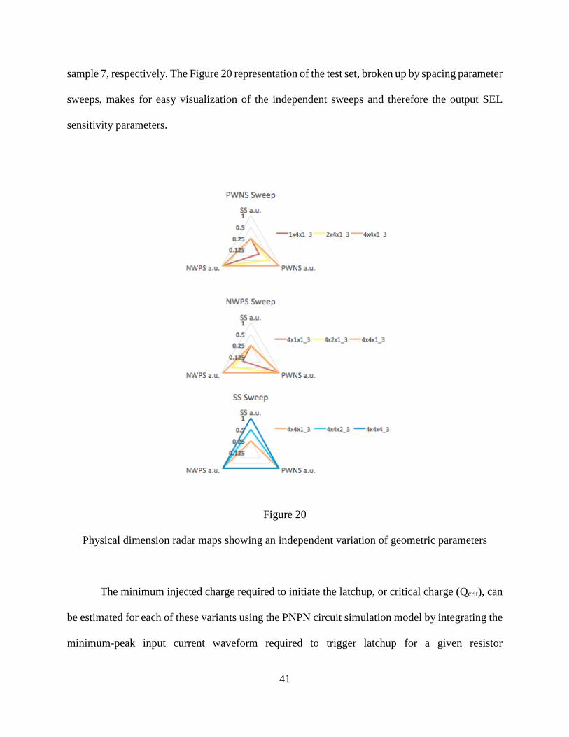
41
sample 7, respectively. The Figure 20 representation of the test set, broken up by spacing parameter
sweeps, makes for easy visualization of the independent sweeps and therefore the output SEL
sensitivity parameters.
Figure 20
Physical dimension radar maps showing an independent variation of geometric parameters
The minimum injected charge required to initiate the latchup, or critical charge (Qcrit), can
be estimated for each of these variants using the PNPN circuit simulation model by integrating the
minimum-peak input current waveform required to trigger latchup for a given resistor

42
configuration. This value will be on the order of hundreds of fC. The critical charge (Qcrit), in turn,
can be translated to a LET threshold value by the rule of thumb from [6]: 1pC/um is approximately
equivalent to a LET of 100 MeV cm-2 mg-1. The experimental data should validate this estimation.
Extracting Qcrit values in the PNPN circuit simulation and translating the RCW and RBS
resistance values respectively back to SS and PWNS spacing values, the dimensional contour plot
in Figure 21 is created showing the effect of combined SS and PWNS spacing values on Qcrit.

43
Figure 21
Example Qcrit vs. geometry contour plot
Figure 21 illustrates a variation in critical charge to induce SEL as a function of PWNS
spacing from 4x to 1x and SS spacing from 1x to 2.5x. The empty corner of the plot shows a
latchup-immune region of operation. This plot shows the direction and slope of the input spacing
values translated to the output SEL sensitivity parameter, Qcrit. At 1x values of PWNS spacing, it
was not possible to trigger latchup in the structure in simulation when SS was above a value of
2.5x because the resulting increase in coupling resistance diminishes the feedback. Across this
combined variation, Qcrit varies by 20% around the average value of 0.573 pC when latchup is
possible. The empty corner simulation result strongly supports the hypothesis that latchup
immunity is achievable by strategically varying PWNS, NWPS, and SS spacing parameters.
According to the Figure 17 [8], the critical charge should be around 220 fC or 0.220 pC. The

44
control sample estimate of Qcrit is 463 fC or 0.463 pC. This estimate is on the same order of
magnitude as the critical charge quoted in [8], which shows that the size of the BJT model
collection volume needs to be tuned further until it matches the data from [8]. However, the contour
still gives an illustration of the effect of varying geometry on SEL sensitivity, and can be used to
understand how latchup immunity may be achieved.
Conclusion
Evidence from the literature supports the hypothesis of geometry affecting SEL sensitivity.
These trends must be uniquely characterized for a technology process such that a CMOS designer
can evaluate SEL sensitivity of a design. By relating measurable resistance values to a latchup
simulation model, changes in design spacing parameters can be evaluated to achieve latchup
immunity above a given threshold. Relating the resistance sensitivity to changes in SS spacing,
PWNS spacing, and NWPS spacing must be done in independent sweeps and can be achieved with
a minimum of 7 samples to characterize three physical parameters. This method of characterization
is extendable to any CMOS technology node and provides direct feedback to designers on what
changes in their device geometry are worthwhile.

45
CHAPTER IV
TEST CHIP DESIGN FOR PARAMETRIC ANALYSIS OF SEL
Introduction
Fabrication and testing considerations are detailed in the following chapter. The geometric
variants are designed and fabricated in a 180 nm CMOS process for SEL characterization and
electrical latchup characterization. The radiation test chip contains the PNPN latchup test devices
connected in parallel with the ability to switch modes, depending on the type of latchup
characterization to be performed. There are two modes of operation: Single Event Latchup Test
Mode, which consists of many PNPN devices for rapid data gathering in a particle beam and
Electrical Latchup Test Mode, which consists of a single PNPN device for electrical latchup
characterization, obtaining I-V curves on the parasitic BJTs, and measuring the model’s resistance
values. A “sample” consists of a chain of radiation test blocks and a single electrical test block.
Switching modes requires setting the state of the MODE pin. The blocks are connected to ground
by active-low NMOS switches. The gate terminals of these switches are attached to the MODE
pin except for the single Electrical Latchup Test device, which is enabled by a guard-ringed
inverter when all other Radiation Latchup Test devices are disabled. Figure 22 shows an example
circuit diagram of a single test block.

46
Figure 22
Diagram of a sample test block with electrical latchup and single event latchup modes
The geometric characterization of the process requires a minimum of 7 variants. However,
there are two additional parameters for comparison to the 7-sample geometric characterization test
set in Table 1: the guard rings (GR) shown in Figure 11 and substrate contact density (SC).
Including GR and SC along with two more geometric design corners: the 1x1x4 variant, for
evaluating combined SEL sensitivity to geometric variation and the WC variant, with minimum-
allowable SS spacing. These additions brings the total number of implemented variants in the test
chip to sixteen, detailed in Table 2:

47
Table 2
Implemented Geometric Variant Test Set
Sample Short Name PWNS NWPS SS GR SC
1 1x1x4_1 1x 1x 4x No 1
2 1x4x1_3 1x 4x 1x No 1/3
3 2x4x1_3 2x 4x 1x No 1/3
4 4x1x1_3 4x 1x 1x No 1/3
5 4x2x1_3 4x 2x 1x No 1/3
6 4x4x1_1 4x 4x 1x No 1
7 4x4x1_2 4x 4x 1x No ½
8 4x4x1_3 4x 4x 1x No 1/3
9 4x4x2_3 4x 4x 2x No 1/3
10 4x4x4_3 4x 4x 4x No 1/3
11 GR_1x1x4_1 1x 1x 4x Yes 1
12 GR_1x4x1_3 1x 4x 1x Yes 1/3
13 GR_4x1x1_3 4x 1x 1x Yes 1/3
14 GR_4x4x1_3 4x 4x 1x Yes 1/3
15 GR_4x4x4_3 4x 4x 4x Yes 1/3
16 WC_3 >4x >4x <1x No 1/3
A switched matrix of four shared VDD buses, and four shared GND buses controls the test
set in Table 2 to save on test time. Table 3 details the connectivity matrix:
Table 3
Test Chip Connectivity Matrix
Short Name VDD1 ANODE1 VDD2 ANODE 2 VDD3 ANODE 3 VDD4 ANODE 4
GND1 CATHODE1
4x4x1_3 WC_3 1x1x4_1 GR_1x1x4_1
GND2 CATHODE2
2x4x1_3 1x4x1_3 4x2x1_3 4x1x1_3
GND3 CATHODE 3
4x4x2_3 4x4x4_3 4x4x1_2 4x4x1_1
GND4 CATHODE4
GR_4x4x1_3 GR_1x4x1_3 GR_4x1x1_3 GR_4x4x4_3

48
A maximum of four variants can thus be tested at once by energizing all voltage buses and then
connecting a single ground bus. For example, if GND1 is connected when all voltages (VDD1,
VDD2, VDD3, and VDD4) energized then 4x4x1, WC_3, 1x1x4, and GR_1x1x4 are the devices
under test. This strategy reduces the required test time by a maximum factor of 4. There are shared
anode and cathode bus connections between variants, as well, to induce the latchup effect. Any
devices that are not under test have their cathodes charged to VDD to prevent any unwanted
latchup that may skew experimental results.
PNPN Layout
As noted in Chapter III, the “worst-case” geometric combination (4xPWNS, 4xNWPS,
1xSS) serves as the control sample for the test set in Table 1 and Table 2 such that any variation
will result in improved SEL response. Moreover, measuring SEL sensitivity to changes in
geometric parameters requires that the devices exhibit latchup under test. The “1xSS” spacing is
practically defined as the minimum required space to fit the guard ring (GR) diffusion around the
anode without changing any other physical dimensions such that results are directly comparable
between GR and no GR variants. For this reason, the 4x4x1 variant of the test set is not the
minimum-allowable SS spacing case because the SS spacing could be smaller, but would not allow
for a GR to fit around the anode and still meet design rules. A variant with minimum anode-cathode
(SS) spacing was added to include the SS worst case, denoted as “WC_3” in Table 2, but this
variant is very similar to sample 1, the 4x4x1 control variant. Only WC_3 implements the
minimum-allowable SS spacing because the independent geometric sweeps defined in the previous
chapter are referenced to the control sample. At advanced sub-micron technology nodes, there are
already many non-linear physical mechanisms at work, and conflating multiple mechanisms by
changing multiple dimensions complicates analysis. Therefore, a near-minimum spacing was

49
chosen to allow computation of linear difference equations relating SEL sensitivity to geometric
spacing as well as direct comparisons between GR and non-GR variants.
There are two geometric best cases of note among the sixteen variants of the test set. The
first is without the GR: sample 1 in Table 2, 1xPWNS, 1xNWPS, and 4xSS (1x1x4), which is the
complement of sample 7 in Table 2, the 4x4x1 control variant. The 1x1x4 variant represents a
practical configuration because minimizing the trigger resistance while maximizing the coupling
resistance of the PNPN structure is dually desirable. Moreover, the 1x1x4 variant serves as an
empirical superposition corner of the geometric characterization and it will test the non-linearity
of the SEL response to geometry. If the 1x1x4 sample proves to be significantly different from a
linear superposition of the independent sweeps of SS, PWNS, and NWPS, then the result would
suggest a more complicated interplay of SEL mechanisms than a first-order linear difference
equation can capture.
The other best case is the guard ring (GR) version of the geometric sweep variants: sample
11 in Table 2. The GR is a standard latchup mitigation technique [8]. Recall from Chapter II
Background, Figure 11, a GR consists of a reverse-biased diffusion surrounding the anode or
cathode. The GR diffusion attracts minority carriers and shunts them the power rail before the
carriers can drift to the emitter of the parasitic BJT. The GR effectively breaks the PNPN parasitic
path that causes latchup. In the case of these test variants, an n-type GR diffusion, hard-tied to
VDD via metal 1, surrounds the p-type anode and serves to attract and shunt any excess electrons
that are generated near the anode. Literature has shown this to be an especially useful technique to
make sure that a structure does not latchup.
The last parameter under study, the substrate contact (SC), is a low-resistance connection
to the p-type substrate (reference ground potential). This contact ensures a stable ground. SC

50
density is an issue for compact CMOS circuits because resistance builds up along materials as they
extend away from the SC. This causes a “floating” ground effect at devices that are distant from
the SC, thereby reducing the required voltage to forward-bias a parasitic BJT - ergo reducing the
energy required to trigger SEL. Because of this floating ground effect, it is recommended to meet
a sufficiently high density of SC such that there is a strong contact to ground and voltage cannot
build up. This work evaluates SC density at the macro level with 16-48 devices per SC. Figure 23
shows an example illustration of different SC densities. SC = 1 is less susceptible than SC = 1/3
because there are more devices per SC in the 1/3 variations so the SC has to support more devices.
The SC density of a variant is denoted by the “_1”, “_2”, or “_3” that correspond to SC density
values of 1, 1/2, and 1/3 respectively.

51
Figure 23
Diagram of low (top) and high (bottom) substrate contact (SC) densities
Electrical Latchup Considerations
Two latchup testing standards should be noted for their significance in microchip latchup
qualification: IEEE 1181 [13] and JEDEC JESD78 [17]. These two standards detail the standard
latchup PNPN structure [13], and testing standards for inducing and measuring electrical latchup
[17] (not radiation-induced) Electrical latchup tests are performed to characterize the PNPN
structures prior to radiation testing. Electrical latchup tests extract the trigger point (VTrig, ITrig) and
holding point (VHold, IHold) of the PNPN structures. The trigger point and holding point values are
the same for SEL and electrical latchup because even though the method of inducing latchup is
different, the resulting physical phenomenon is the same [6].

52
IEEE 1181 details the test structures that are acceptable for parameterizing a silicon process
such as the PNPN structure detailed in the background. The IEEE 1181 standard refers to the
PNPN structure as a “silicon-controlled rectifier” (SCR), or “trigger diode.”
JESD78 [17] provides a detailed procedure for connecting and running the two critical tests
for characterizing electrical latchup: the Overvoltage Test for power pins (VDD and GND in the
case of the PNPN test structure) and the I-Test for signal pins (Anode and Cathode in the case of
the PNPN test structure).
The circuit in Figure 24 [17] shows the configuration and procedure required to apply the
I-Test to an arbitrary CMOS IC. Initially, the PNPN structure is in equilibrium as it would be when
performing nominally, then a transient voltage is applied to the anode or cathode to forward-bias
the BJT junction, inject minority carriers, and initiate latchup.

53
Figure 24
I-Test circuit diagram, from JESD78 [17]
The circuit in Figure 25 [17] shows the configuration and procedure required to apply the
overvoltage test to an arbitrary CMOS IC. The overvoltage test covers worst case of latchup
susceptibility with respect to voltage, which is why the test is applied, as the name of the test
suggests, at an elevated operating voltage. Details involving classification and failure criteria of
the devices depend on I-V characteristics extracted by Gummel plots of the parasitic BJTs. Refer
to JESD78 [17] for specific details on classification and test conditions.

54
Figure 25
Overvoltage test circuit diagram, from JESD78 [17]
Single-Event Latchup Testing Considerations
Temperature has a direct correlation to the latchup sensitivity of a CMOS device because
the carrier equilibrium concentrations are more plentiful at higher temperatures [7]. It is required
in radiation testing to test at worst-case temperature, and to track ambient temperature during the
test.
The high-LET particles that come from deep space galactic cosmic rays (GCRs),
mentioned in the Chapter II Background of this document, are usually responsible for triggering

55
latchup in space electronics. The rigor of radiation effects testing depends on mission assurance.
For example, a deep space satellite that leaves the protection of Earth’s magnetic field will require
testing to a higher LET than a satellite that stays in low-earth orbit. A heavy-ion particle beam is
required to simulate the high-LET particles. There are several facilities in the United States such
as the cyclotron accelerators at Texas A&M University Cyclotron Institute (TAMU) or Lawrence
Berkeley National Lab (LBNL). Each has different advantages; TAMU allows for open-air testing
and may be ideal for cryogenic dewar testing, but switching ion species (therefore LET) is a time-
consuming process, sometimes taking longer than an hour, whereas LBNL provides a “cocktail”
of ion species that are selectable with a call to the control room. However, the output of the LBNL
heavy-ion beam is contained in a vacuum so the equipment setup and teardown is much more
involved and requires additional logistical preparation.
For the heavy-ion radiation test to be statistically significant there must be a sufficient
number of latchup events to eliminate uncertainty or, if the test structure is immune to latchup, a
significant fluence of particles must be reached to reduce the standard error to an acceptable level.
According to Johnston [14], parts should be tested to a fluence of 107 particles/cm2 or 100 SEL
events (whichever comes first) at a flux between 104 particles/cm2*s to 105 particles/cm2*s
depending on the rate of upsets. For this reason, equipment automation is an important part of
radiation effects testing as the rate of latchup may become overwhelming to human operators.
The SEL cross section measurements measured by Marshall et al. (upsets/cm2) [7] is used
as a reference to calculate how many devices are needed to produce statistically significant results.
Minimum cross-section required to obtain 100 SEL events at a fluence of 107 was calculated to be
approximately 10000 um2 per sample. Estimated sensitive area is shown in Figure 26 after Artola
laser testing [8]: it is the combined area in the N-well and the area between the two sources. This

56
sensitive area changes with the geometry of the variants, so each variant requires a different
number of devices to reach a total sensitive area of 10000 um2.
Figure 26
The sensitive area of a laser latchup structure, after Artola [8]
Sensitive area per device divides the total required area (10000 um2) to give the total number of
required devices per sample. The devices themselves group into sixteen parallel devices to form a
test block. Figure 22 shows two different versions of a test block: the SEL test block and the
electrical latchup test block. The SEL test blocks are connected in parallel to reach the required

57
10000 um2 sensitive area for the radiation test. The electrical latchup test block, consisting of a
single device, is at the end of the parallel set of radiation test blocks.
During all latchup tests, electrical and radiation-induced, the power supply must be current-
limited such that the devices do not destructively damage themselves before a statistically
significant sample size is reached as recommended by JESD78 [17]. Any test following a latchup
event must allow sufficient time for cool-down to thermal equilibrium such that the elevated
temperatures produced by latchup currents do not bias the experimental results.
Conclusions
Care must be taken when designing a chip for radiation effects testing because these tests
can be expensive. Simultaneously testing multiple samples reduces the required test time.
Arranging the samples in a switched matrix with a shared bus system reduces the required number
of pins on the IC. Extracting resistance parameters with I-V characterization of the parasitic BJTs
and extracting common-emitter gain with the overvoltage will inform an accurate latchup
simulation model. Latchup-immune devices will emerge in the electrical latchup characterization
but perform characterization on a single device. The system must be capable of switching between
electrical latchup and radiation latchup modes. Incorporating these characteristics in an SEL test
set will enable comprehensive geometric characterization of the silicon process in which the
devices are manufactured.

58
CHAPTER V
DISCUSSION
As additional advanced technology nodes mature into space-grade qualification, single-
event latchup will remain a challenge that electronics designers will need to address.
Unfortunately, the task is not a simple one because each process is slightly different and details of
electronics manufacturing are becoming more opaque. Silicon manufacturers are protective of
their intellectual properties. Opacity limits the analytical tools that are available to designers of
space-grade electronics who must find a way to meet stringent qualification standards.
This work shows that existing data may be used to provide useful tools to understand the
limitations and response to geometric differences in CMOS well structures. SEL vulnerability of
a design of given device width and length can be evaluated and produce recommendations for
geometric changes to achieve a particular SEL hardness threshold.
The requirements are simple: extracted resistance-to-spacing mapping for independently
varied SS, PWNS, and NWPS spacing parameters, an accurately tuned circuit simulation model
to estimate the required input charge to cause latchup, and an approximation of latchup sensitivity
mapped to the geometric spacing parameters. The analysis results are unique for each CMOS
process, but the method of extraction should be extendable to any CMOS process.
Statistically measuring this approach for significance will be the next step in the process
and identifying possible non-linear response with respect to various spacing parameters will add
to the predictive power of this method. Remove variants that test spacing parameters that do not

59
show promise for changing the latchup sensitivity from the test set and replace them in future
revisions with samples of intermediate value spacing to further characterize any non-linear
responses.

60
CHAPTER VI
CONCLUSIONS
The method of characterizing a process for its SEL sensitivity shows promise due to its
applicability to existing data [12], [11] used to inform the simulation model. Simulation results
show a sharp borderline with respect to well-to-source spacing, and source-to-source spacing
shows the expected linear response. The well-to-source sharp borderline should be evaluated in
future studies of geometric spacing because it defines the trigger resistance that allows latchup to
occur in the first place. The coupling resistance high value shows promise in preventing latchup
from getting to its final stage even with sufficient trigger resistance to initiate latchup.
Mapping the response of radiation effects to geometric parameters is the benefit of this
work, and the hope is that the radiation tests of the implemented test chip will validate this mapping
or provide information for tuning the simulation model to provide accurate predictive simulations.

61
CHAPTER VII
SIGNIFICANCE
The significance of this work is its applicability to the CMOS designer who is attempting
to produce systems at a target level of assurance without the need to perform rigorous and costly
radiation testing. Relating geometry to SEL susceptibility provides a tool to the designer that
evaluates an arbitrary CMOS well geometry and elucidates spacing-to-SEL tradeoffs that can
guarantee low-risk space electronics without a complete redesign of the system. Furthermore, this
work lays the ground for multi-dimensional and intuitive visual representations of the contour of
the latchup Qcrit versus the geometric spacing variations. This product is particularly useful in the
critical design review and simplifies the complex CMOS geometry to a single 3D model of two
input spacing parameters and an output SEL sensitivity parameter of critical charge.

62
REFERENCES
[1] UNOOSA. Online Index of Objects Launched into Outer Space [Online]. Available:
http://www.unoosa.org/oosa/osoindex/
[2] L. Massengill, "SEU modeling and prediction techniques," in IEEE NSREC Short
Course, 1993, vol. 3, pp. 1-93.
[3] K. Endo, "Earth's Magnetic Field," in Nikkei Science Inc., ed, 2006.
[4] ESA, "South Atlantic Anomaly," ed: European Space Agency, 2012.
[5] L. Adams et al., "A verified proton induced latch-up in space [CMOS SRAM]," IEEE
Transactions on Nuclear Science, vol. 39, no. 6, pp. 1804-1808, 1992.
[6] N. A. Dodds et al., "Effectiveness of SEL Hardening Strategies and the Latchup Domino
Effect," IEEE Transactions on Nuclear Science, vol. 59, no. 6, pp. 2642-2650, 2012.
[7] C. J. Marshall et al., "Mechanisms and Temperature Dependence of Single Event
Latchup Observed in a CMOS Readout Integrated Circuit From 16–300 K," IEEE
Transactions on Nuclear Science, vol. 57, no. 6, pp. 3078-3086, 2010.
[8] L. Artola, G. Hubert, and T. Rousselin, "Single-Event Latchup Modeling Based on
Coupled Physical and Electrical Transient Simulations in CMOS Technology," IEEE
Transactions on Nuclear Science, vol. 61, no. 6, pp. 3543-3549, 2014.
[9] R. R. Troutman, "Latchup in CMOS technologies," IEEE Circuits and Devices
Magazine, vol. 3, no. 3, pp. 15-21, 1987.
[10] A. A. Youssef, L. Artola, S. Ducret, G. Hubert, and F. Perrier, "Analysis of low
temperature on single event Latchup mechanisms by TCAD simulations for applications
down to 50K," in 2016 16th European Conference on Radiation and Its Effects on
Components and Systems (RADECS), 2016, pp. 1-5.
[11] L. Artola et al., "Analysis of Angular Dependence of Single-Event Latchup Sensitivity
for Heavy-Ion Irradiations of 0.18um CMOS Technology," IEEE Transactions on
Nuclear Science, vol. 62, no. 6, pp. 2539-2546, 2015.

63
[12] G. Boselli, V. Reddy, and C. Duvvury, "Latch-up in 65nm CMOS technology: a scaling
perspective," in 2005 IEEE International Reliability Physics Symposium, 2005.
Proceedings. 43rd Annual., 2005, pp. 137-144.
[13] IEEE Electron Devices Society, "IEEE Recommended Practice for Latchup Test Methods
for CMOS and BiCMOS Integrated-Circuit Process Characterization," IEEE Std 1181-
1991, p. 0_1, 1991.
[14] A. H. Johnston, "The influence of VLSI technology evolution on radiation-induced
latchup in space systems," IEEE Transactions on Nuclear Science, vol. 43, no. 2, pp.
505-521, 1996.
[15] D. McMorrow et al., "Laser-Induced Latchup Screening and Mitigation in CMOS
Devices," in 2005 8th European Conference on Radiation and Its Effects on Components
and Systems, 2005, pp. C22-1-C22-7.
[16] J. M. Hutson, R. D. Schrimpf, and L. M. Massengill, "The Effects of Scaling and Well
and Substrate Contact Placement on Single Event Latchup in Bulk CMOS Technology,"
in 2005 8th European Conference on Radiation and Its Effects on Components and
Systems, 2005, pp. PC24-1-PC24-5.
[17] JEDEC IC Latch-up Test JESD78A, 2005.

64
VITA
Matt Joplin was born September 19th, 1992 in St. Joseph, Missouri to Russell and Yavonda
Joplin the fourth of five brothers. He graduated in 2011 from Signal Mountain High School in
Signal Mountain, Tennessee and attended the University of Tennessee at Knoxville, Chattanooga
State Community College, and the University of Tennessee at Chattanooga. He graduated with his
Bachelor’s of Science in Electrical Engineering in December 2015 and returned to work on his
Master’s Degree at UTC the following semester as a Graduate Research Assistant for Dr. Daniel
Loveless in the Electrical Engineering department. In the summer of 2016, he got the opportunity
to co-op with SpaceX in Redmond, WA working as a radiation effects associate engineer for eight
months before returning to continue his master’s degree in Fall 2017. He hopes to pursue a career
in the field of space electronics after completing his Master’s of Science in Electrical Engineering.