Embed Size (px)
Citation preview
A Micro-Undulator Fabricated by LIGA Processes*
L.R. Turner, A. Nassiri, F. E. Mills, and S. Kim Advanced Photon Source
Argonne National Laboratory 9700 South Cass Avenue
Argonne, Illinois 60439 USA
Alan Feinerman Microfabrications Laboratory
University of Illinois at Chicago Chicago, Illinois 60607, USA
bv 8 contractor of the U. S. Gwernment under contract No. W-31-lqOENG-38. Accordingly. the U. S Government retains a nonexclusive, royalty-free license to publish or reproduce the published form of this contribution, or allow others to do 90. for
*Work supported by the U. S. Department of Energy, Office of Basic Sciences, under Contract No. W-31-109-ENG-38.
L

DISCLAIMER
Portions of this document may be illegible in electronic image products. Images are produced from the best available original document.
A Micro-Undulator Fabricated by LIGA Processes* L.R. Turner, A. Nassiri, F. E. Mills, and S. Kim
Advanced Photon Source Argonne National Laboratory 9700 South Cass Avenue
Argonne, Illinois 60439 USA
Alan Feinerman Microfabrications Laboratory
University of Illinois at Chicago Chicago, Illinois 60607, USA
Abstract--An undulator of period 1 mm has been designed as part of a series of studies toward table-top synchrotron radiation sources. The undulator consists of a silver conductor embedded in poles and substrate of nickel-iron. Computations predict a field pattern of appropriate strength and quality if the current can be prevented from shunting from the silver across the nickel- iron poles, either through insulation or through slotted poles. A ten-scale model has been fabricated and measured; a full-scale model has also been constructed by conventional machining tech- niques, but has not yet been measured.
I. INTRODUCTION Recognizing the value of a table-top synchrotron light
source for medical uses and other purposes, a group of researchers at Argonne National Laboratory (ANL), the Micro- fabrications Laboratory at the University of Illinois in Chicago, the University of Wisconsin, and the Technical University of Berlin have begun studies toward that end [ 11.
An important part of these studies is the design, construc- tion, and testing of an undulator of period 1 mm. Undulators and wigglers are devices that are inserted into an electron or positron beam to produce x-rays. Such an insertion device has its magnetic field in a direction transverse to the beam direc- tion and alternating periodically along the beam direction. The field causes the particles of the beam to oscillate, and thus to generate x-rays. The insertion device is called an undulator if the radiation emitted from neighboring periods is coherent, and a wiggler if it is incoherent. Wigglers and undulators each have a characteristic spectrum of radiation.
II. MICROFABRICATION: LIGA The undulator will be fabricated by LIGA (a German acro-
nym for Lithography, Electroforming, and Molding) processes [2]. In LIGA, x-rays with a wavelength less than 1 nm are used to expose a photosensitive layer, typically polymethyl- methacrylate (PMMA). The PMMA is usually applied over a plating base, and when the exposed PMMA regions are removed in a highly selective developer, metal can be electro- plated into the PMMA recases defined by the x-rays. The short wavelength minimizes diffraction, and the metal features can be electroplated several hundred microns high with edge runouts of less than 0.1 micron 131.
Manuscript received 12 June 1995. *Work supported by the U. S. Department of Energy, Office of
Basic Sciences, under Contract No. W-3 1 - 109-ENG-38.
m. THE UNDULATOR
The undulator can operate in the electron beam from the linac of the Advanced Photon Source (APS), now being com- missioned at Argonne National Laboratory (ANL) and funded by the U. S. Department of Energy. With the positron produc- tion target retracted from the beamline, the linac could acceler- ate electrons to an energy of 750 MeV. The geometry of the undulator consists of a silver conductor embedded in poles and substrate of nickel-iron. Silver is chosen for its high electrical conductivity and its softness. Nickel-iron is chosen for its high permeability and suitable mechanical properties [4]. In the analysis, the copper conductivity was taken as 61.0 x lo6 S/m and the 75%-nickel, 25%-kon alloy substrate was taken to have a conductivity of 6.67 x lo6 and a permeability of 1oooO. The geometrical parameters appear in Table I and the operating parameters in Table II.
TABLE I Geometrical Parameters of the Micro-Undulator
Parameter Value
Period 1.0 mm
Gap 0.6 mm
Conductor Height 0.2 mmx
Conductor Thickness 0.2 mm
Pole Height 0.2 mm
Pole Thickness 0.3 mm
Pole Width 0.7 mm
TABLE I1 Operating Parameters of the Micro-Undulator
Parameter Value
Beam Energy
Deflection Parameter ku
Field Strength
Excitation Current
Excitation pulse length
650 - 750 MeV
0.0467
0.5 T
280 A
J 0 - 2 0 p
i . . ,, ,.,., . ‘..... . _.. _.... . ..
The winding pattern is shifted one half period between the top and bottom halves of the undulator so that for the two halves, the currents in the beam direction oppose each other but in the transverse direction, currents flow in the same direc- tion. Earlier designs with currents in the same direction top and bottom led to a field gradient across the central region of the undulator.
IV. ELECTROMAGNETIC MODELING A shortened (2-period) version of the undulator was mod-
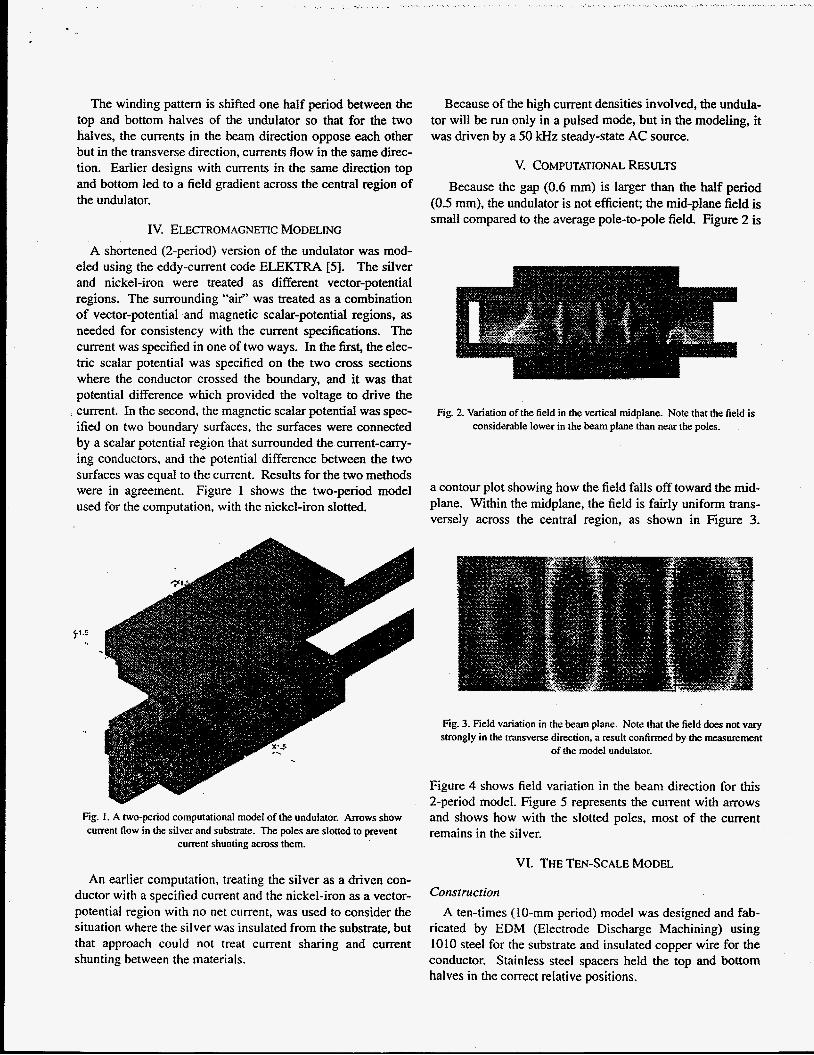
eled using the eddy-current code ELEKTRA [5 ] . The silver and nickel-iron were treated as different vector-potential regions. The surrounding “air” was treated as a combination of vector-potential and magnetic scalar-potential regions, as needed for consistency with the current specifications. The current was specified in one of two ways. In the first, the elec- tric scalar potential was specified on the two cross sections where the conductor crossed the boundary, and it was that potential difference which provided the voltage to drive the current. In the second, the magnetic scalar potential was spec- ified on two boundary surfaces, the surfaces were connected by a scalar potential region that surrounded the current-cany- ing conductors, and the potential difference between the two surfaces was equal to the current. Results for the two methods were in agreement. Figure 1 shows the two-period model used for the computation, with the nickel-iron slotted.
Because of the high current densities involved, the undula- tor will be run only in a pulsed mode, but in the modeling, it was driven by a 50 kHz steady-state AC source.
V. COMPUTATIONAL RESULTS Because the gap (0.6 mm) is larger than the half period
(0.5 mm), the undulator is not efficient; the mid-plane field is small compared to the average pole-to-pole field. Figure 2 is
Fig. 1. A two-period computational model of the undulator. Arrows show current Row in the silver and substrate. The poles are slotted to prevent
cumnt shunting across them.
An earlier computation, treating the silver as a driven con- ductor with a specified current and the nickel-iron as a vector- potential region with no net current, was used to consider the situation where the silver was insulated from the substrate, but that approach could not treat current sharing and current shunting between the materials.
Fig. 2. Variation of the field in the vertical midplane. Note that the field is considerable lower in the beam plane than near the poles.
a contour plot showing how the field falls off toward the mid- plane. Within the midplane, the field is fairly uniform trans- versely across the central region, as shown in Figure 3.
Fig. 3. Field variation in the beam plane. Note that the field does not vary strongly in the transverse direction. a result confirmed by the measurement
of the model undulator.
Figure 4 shows field variation in the beam direction for th is 2-period model. Figure 5 represents the current with arrows and shows how with the slotted poles, most of the current remains in the silver.
VI. THE TEN-SCALE MODEL
Construction A ten-times ( IO-rnm period) model was designed and fab-
ricated by EDM (Electrode Discharge Machining) using 1010 steel for the substrate and insulated copper wire for the conductor. Stainless steel spacers held the top and bottom halves in the correct relative positions.
04 c
03 -
60 a0 0.0 60 0.a 0.0
OS fS 00 A0
OD 00 0.0 00 -25 I -1B -1.1 - -o* -
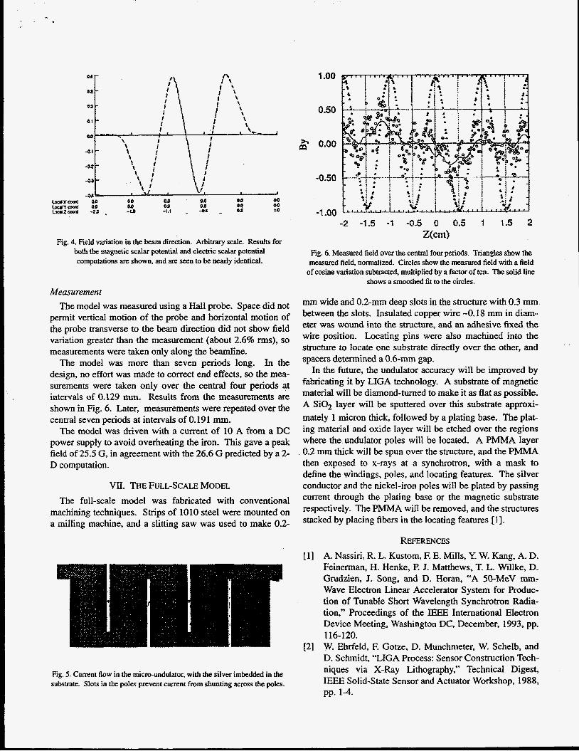
Fig. 4. Field variation in the beam direction. Arbitrary scale. Results for both the maguetic scalar potential and electric scalar potential computations are shown, and are Seen to be nearly identical.
Measurement The model was measured using a Hall probe. Space did not
permit vertical motion of the probe and horizontal motion of the probe transverse to the beam direction did not show field variation greater than the measurement (about 2.6% rms), so measurements were taken only along the beamline.
The model was more than seven periods long. In the design, no effort was made to correct end effects, so the mea- surements were taken only over the central four periods at intervals of 0.129 nun. Results from the measurements are shown in Fig. 6. Later, measurements were repeated over the central seven periods at intervals of 0.19 1 mm.
The model was driven with a current of 10 A from a DC power supply to avoid overheating the iron. This gave a peak field of 25.5 G, in agreement with the 26.6 G predicted by a 2- D computation.
vu. THE FULL-SCALE MODEL The full-scale model was fabricated with conventional
machining techniques. Strips of 1010 steel were mounted on a milling machine, and a slitting saw was used to make 0.2-
Fig. 5. Current flow in the micro-undulator. with the silver imbedded in the Substrate. Slots in the poles prevent current from shunting across the poles.
1 .oo
0.50
0.00
-0.50
1 1.5 2
Fig. 6. Measured field over the central four periods. Triangles show the measured field. normalized. Circles show the measured field with a field
of cosine variation subtracted, multiplied by a factor of ten. The solid line shows a smoothed fit to the circles.
mm wide and 0.2-mm deep slots in the structure with 0.3 mm between the slots. Insulated copper wire -0.18 mm in diam- eter was wound into the structure, and an adhesive fixed the wire position. Locating pins were also machined into the structure to locate one substrate directly over the other, and spacers determined a 0.6-mm gap.
In the future, the undulator accuracy will be improved by fabricating it by LIGA technology. A substrate of magnetic material will be diamond-turned to make it as flat as possible. A Si02 layer will be sputtered over this substrate approxi- mately 1 micron thick, followed by a plating base. The plat- ing material and oxide layer will be etched over the regions where the undulator poles will be located. A PMh4A layer 0.2 mm thick will be spun over the structure, and the PMMA then exposed to x-rays at a synchrotron, with a mask to define the windings, poles, and locating features. The silver conductor and the nickel-iron poles will be plated by passing current through the plating base or the magnetic substrate respectively. The PMMA will be removed, and the structures stacked by placing fibers in the locating features [I].
REFERENCES A. Nassiri, R. L. Kustom, F. E. Mills, Y. W. Kang, A. D. Feinerman, H. Henke, P. J. Matthews, T. L. Willke, D. Grudzien, 3. Song, and D. Horan, “A 50-MeV mm- Wave Electron Linear Accelerator System for Produc- tion of Tunable Short Wavelength Synchrotron Radia- tion,” Proceedings of the IEEE International Electron Device Meeting, Washington DC, December, 1993, pp. 116-120. W. Ehrfeld, F. Gotze, D. Munchmeter, W. Schelb, and D. Schmidt, “LIGA Process: Sensor Construction Tech- niques via X-Ray Lithography,” Technical Digest, IEEE Solid-state Sensor and Actuator Workshop, 1988, pp. 1-4.
[3] €I. Guckel, T. R. Christenson, K. J. Skrobis, D. D. Den- ton, B. Choi, E. G. Lovell, J. W. Lee, s. s. Bajikar, and T. W. Chapman, “Deep X-Ray and UV Lithographies for Micromechanics,” Proceedings of IEEE Solid State Sen- sor and Actuator Workshop, 1990, pp- 118-122.
[4] R. M. Bozorth, Ferromagnetism. (New York, D. Van Nostrand, 1951). Ch. 5, Iron-Nickel Alloys.
[SI The 3-D eddy-current code ELEKTRA is available from Vector Fields, Ltd., Oxford, UK.