Embed Size (px)
Citation preview

The Pennsylvania State University
The Graduate School
Department of Mechanical and Nuclear Engineering
A MODIFIED 3! METHOD FOR THERMAL CONDUCTIVITY
MEASUREMENT OF ONE-DIMENSIONAL NANOSTRUCTURES
A Thesis in
Mechanical Engineering
by
Hsiao-Fang Lee
" 2009 Hsiao-Fang Lee
Submitted in Partial Fulfillment
of the Requirements
for the Degree of
Master of Science
May 2009

ii
The thesis of Hsiao-Fang Lee was reviewed and approved* by the following:
M. Amanul Haque
Associate Professor of Mechanical Engineering
Department of Mechanical and Nuclear Engineering
Thesis Advisor
Anil K. Kulkarni
Professor of Mechanical Engineering
Department of Mechanical and Nuclear Engineering
Karen A. Thole
Professor of Mechanical Engineering
Head of the Department of Mechanical and Nuclear Engineering
*Signatures are on file in the Graduate School
iii
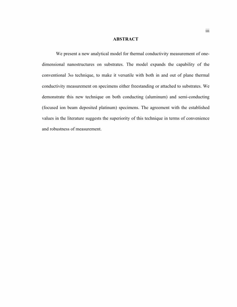
ABSTRACT
We present a new analytical model for thermal conductivity measurement of one-
dimensional nanostructures on substrates. The model expands the capability of the
conventional 3! technique, to make it versatile with both in and out of plane thermal
conductivity measurement on specimens either freestanding or attached to substrates. We
demonstrate this new technique on both conducting (aluminum) and semi-conducting
(focused ion beam deposited platinum) specimens. The agreement with the established
values in the literature suggests the superiority of this technique in terms of convenience
and robustness of measurement.

iv
TABLE OF CONTENTS
LIST OF FIGURES .....................................................................................................vi
ACKNOWLEDGEMENTS.........................................................................................viii
Chapter 1 Introduction ................................................................................................1
1.1 Thermal Characterization of Nanostructures.................................................1
1.2 Motivation of This Study...............................................................................2
1.3 Reference.......................................................................................................4
Chapter 2 Literature Review.......................................................................................7
2.1 Thermal Conductivity Measurement by 3! method .....................................8
2.1.1 Line Heater on Substrate.................................................................9
2.1.2 Thin Film on Substrate....................................................................11
2.1.3 Suspended Wire ..............................................................................14
2.2 Strain Effects on Thermal Conductivity........................................................18
2.3 Reference.......................................................................................................21
Chapter 3 Analytic Modeling of 3! Method ..............................................................23
3.1 Introduction of 3! Method............................................................................23
3.2 Continuity Equation.......................................................................................25
3.3 1-D Heat Conduction Equation with Heat Source ........................................26
3.4 1-D Heat Conduction Equation with Heat Source and Heat Sink.................26
3.5 Solution of 1-D Heat Conduction Equation with Heat Source and Heat
Sink................................................................................................................28
3.6 Reference.......................................................................................................32
Chapter 4 Experimental Method.................................................................................33
4.1 Sample Preparation........................................................................................33
4.2 Experimental Set-up ......................................................................................35
4.2.1 Main Apparatus...............................................................................35
4.2.2 Cryogenic Station............................................................................36
4.3 Calibration .....................................................................................................37
4.4 Reference.......................................................................................................38
Chapter 5 Results and Discussion...............................................................................39
5.1 Aluminum Film .............................................................................................39
5.1.1 Temperature Dependence of Resistance of Aluminum Film..........40
5.1.2 Measurement of Thermal Conductivity ..........................................41

v
5.2 Focused Ion Beam Deposited Platinum Nanowire........................................44
5.3 Conclusion.....................................................................................................48
5.4 Reference.......................................................................................................50

vi
LIST OF FIGURES
Figure 2-1: Measurement structure schematic proposed by McConnel . . . . . . . . . . . 8
Figure 2-2: Side view of geometry of line heater on substrate . . . . . . . . . . . . . . . . . . 9
Figure 2-3: Four pads patterned metal film on amorphous substrate . . . . . . . . . . . . .10
Figure 2-4: Geometry of the thin file thermal conductivity measurement . . . . . . . . .11
Figure 2-5: The real part of temperature oscillation as function of frequency . . . . . .12
Figure 2-6: A two-layer structure of 3! applications . . . . . . . . . . . . . . . . . . . . . . . . .13
Figure 2-7: (a) a thin line (b) a wide line . . . . . . . . . . . . . . . . . . . . . . . . . . . . . . . . . . 13
Figure 2-8: Illustration of the four-probe configuration of a filament-like specimen
. . . . . . . . . . . . . . . . . . . . . . . . . . . . . . . . . . . . . . . . . . . . . . . . . . . . . . . . . .14
Figure 2-9: Circuits of voltage approximated current source . . . . . . . . . . . . . . . . . . . 16
Figure 2-10: Schematic of traditional and DC offset added 3! method . . . . . . . . . . . .16
Figure 2-11: Relationship between electrical and thermal functions . . . . . . . . . . . . . . 17
Figure 2-12: The image of suspended silicon nanowire and the schematic of this
device . . . . . . . . . . . . . . . . . . . . . . . . . . . . . . . . . . . . . . . . . . . . . . . . . . . . 17
Figure 2-13: Relationship between thermal conductance and temperature . . . . . . . . . .18
Figure 2-14: Thermal conductivity as a function of temperature and strain . . . . . . . . .19
Figure 2-15: Thermal conductivity and mechanical strains . . . . . . . . . . . . . . . . . . . . . .20
Figure 3-1: Principal of 3! method . . . . . . . . . . . . . . . . . . . . . . . . . . . . . . . . . . . . . . .23
Figure 3-2: 3! method . . . . . . . . . . . . . . . . . . . . . . . . . . . . . . . . . . . . . . . . . . . . . . . . .24
Figure 3-3: Geometry of wire-on-substrate . . . . . . . . . . . . . . . . . . . . . . . . . . . . . . . . .27
Figure 4-1: SEM image of aluminum specimen . . . . . . . . . . . . . . . . . . . . . . . . . . . . . 34
Figure 4-2: Schematic of 3! technique applied on FIB-deposited Platinum . . . . . . . 34

vii
Figure 4-3: Experimental set-up of 3! technique . . . . . . . . . . . . . . . . . . . . . . . . . . . .37
Figure 4-4: 3! voltage measurement by using silver line heater on glass substrate
sample geometry . . . . . . . . . . . . . . . . . . . . . . . . . . . . . . . . . . . . . . . . . . .38
Figure 5-1: Temperature dependence of resistance of aluminum film . . . . . . . . . . . 40
Figure 5-2: The measured
!
V3" and expected
!
V3" of aluminum thin film . . . . . . . . . 42
Figure 5-3: Thermal conductivity of aluminum thin film . . . . . . . . . . . . . . . . . . . . . 43
Figure 5-4: The proportional relationship between
!
V3" of aluminum thin film and
!
I0
3
. . . . . . . . . . . . . . . . . . . . . . . . . . . . . . . . . . . . . . . . . . . . . . . . . . . . . . . . . 43
Figure 5-5: The length dependence on thermal conductivity of aluminum thin film
. . . . . . . . . . . . . . . . . . . . . . . . . . . . . . . . . . . . . . . . . . . . . . . . . . . . . . . . . 44
Figure 5-6: Resistance of FIB platinum . . . . . . . . . . . . . . . . . . . . . . . . . . . . . . . . . . .45
Figure 5-7: Components of FIB platinum . . . . . . . . . . . . . . . . . . . . . . . . . . . . . . . . . 45
Figure 5-8: Temperature dependence of resistance of FIB platinum . . . . . . . . . . . . .46
Figure 5-9: The measured
!
V3" for FIB-deposited Pt nanowire . . . . . . . . . . . . . . . . . 47
Figure 5-10: The average temperature change of FIB Pt nanowire . . . . . . . . . . . . . . .48
Figure 5-11: The conventional 3! setup . . . . . . . . . . . . . . . . . . . . . . . . . . . . . . . . . . . 49

viii
ACKNOWLEDGEMENTS
I would like to express my sincere gratitude to my adviser for bringing me into
the research field of nanotechnology. I can’t approach to the present achievement without
his advice and encouragement, especially during my frustrated time.
Besides, I want to thank my dear friends, Benedict and ChengIng, for helping me
to solve problems and giving me practical suggestions. They are not only wise teachers
but also nice friends. Moreover, I appreciate my lab mates, Mohan and Sandeep for
preparing devices of my experiments, and Jiezhu for discussing 3! method with me.
I am very grateful to my parents for supporting me to continue my study. I wish
that they would be proud of my work and myself. Finally, I would like to thank Buddhas
and Buddhadharma for bringing me the mental sustenance and wisdom.

1
Chapter 1
Introduction
1.1 Thermal Characterization of Nanostructures
The rapid progress of fabrication technology of materials and devices with
nanoscale dimensions has brought not only research opportunities of nanostructures but
also industrial applications of nanostructures. There are few kinds of active
nanostructures, for example, nanotubes, thin films, and nanowires.
The most widely used nanostructure, carbon nanotube, has semi-conducting
property and can play the role as electric wires. The novel mechanical, electric,
photoelectric, chemical, and thermal conductive properties of carbon nanotube make it a
highly potential material in biomedical application, energy storage, modern compound
materials, and nano-electronic application. Nanoscale thin films can be made of metal
particles, semi-conducting particles, insulating particles, and polymers. The structures of
thin films are divided into single layer and multi layers (such as superlattice).
Applications of nanoscale thin films are resistors, capacitors, magnetic tape, and
materials in semi-conducting integrated circuits. As for nanowires, they have been used
for sensor technology, solar cells, and also in electronics.
Electrical and thermal transport properties exhibit significant size effects at the
nanoscale because of the pronounced surface-to-volume ratio influence on the surface
and grain boundary scattering processes. Characterization of such size effects and

2
understanding of the fundamental mechanism is especially important for the
microelectronics industry where the critical dimension is rapidly approaching a few
nanometers. The effect of miniaturization is profound on the energy (in the form of heat
dissipation) density in this class of devices, and thermal management in nanoscale
application has been increasingly noticed and studied [1]. Another class of devices,
namely energy conversion, is also deeply impacted by thermal conductivity of materials.
Therefore, recent efforts focus on the use of nano-structured materials for improved
efficiency [2]. While classical concepts on thermal conductivity render it length-scale
independent, there is growing evidence in the literature for the opposite to be true [3,4].
Therefore, thermal characterization of nanoscale materials has been a very active area of
research in the last decade [5,6,7].
1.2 Motivation of This Study
To measure thermal conductivity, one needs to determine the heat flux (typically
set up by an energy source such as electrical heater) across the specimen to acquire the
cross-plane thermal conductivity, and another requires to measure the temperature drop
between two separate points in the same plane to obtain the in-plane thermal
conductivity. In this paper, we focus on the electrical heating and sensing based
techniques, where the specimens are usually equipped with micro-fabricated heater and
sensors [8]. Well-established techniques for measuring cross-plane thermal conductivity
of thin films and nanostructures are the 3! and the steady-state method [9]. Moreover,
the membrane and bridge methods, which require the substrate to be removed and make

3
the specimen freestanding, are used for in-plane thermal conductivity measurement
[10,11].
The conventional 3! technique is versatile in terms of specimen configuration,
such as: line-heater-on-substrate, thin-film-on-substrate, and multilayered-thin-film-on-
substrate. There is a metallic strip deposited on the sample to act as the heating source
and sensing element [12,13]. The strip metal film acts both as a thermometer and a line
heater driven by a periodically oscillating (1!) heat source, i.e. a.c. current source. The
heat generated due to the a.c. current source and the resistance of the line heater (joule
heating) causes the temperature fluctuation of the line heater itself at the frequency 2!,
and it also heats up the underlying sample. Then, the temperature oscillations make the
resistance of line heater varying at 2!. Therefore, voltage oscillations at 3! can be
derived. By measuring the 3! voltage of the line heater, the thermal conductivity of the
underlying sample can be extracted from the amplitude of 3! voltage. When the
specimen is capable of self heating (metals and semiconductors), it is usually released
from the substrate so that the entire heating energy is exploited to set up the temperature
gradient in the specimen and the measured thermal conductivity is unaffected by that of
the substrate [14]. However, the specimen on substrate configuration is closer than
freestanding configuration in representing real life applications as in microelectronic
devices. Also, releasing the specimen requires additional processing steps and careful
considerations on not to affect the specimen itself, which may be difficult to execute on
nanoscale specimens. Therefore, the motivation of the present study is to relax the
requirement for freestanding specimens, which can increase the versatility of the 3!

4
technique. We achieve this by developing an analytical model that accounts for the heat
loss to the substrate so that the thermal conductivity of both the specimen and the
substrate could be measured simultaneously. We demonstrate the new technique on both
metallic (lithographically patterned aluminum) specimen on glass substrate and semi-
conducting focused ion beam (FIB) deposited platinum specimen on silicon substrate
with an insulating thermal oxide layer. It is important to note that the FIB deposited
materials have received increasing attention in nano-heaters, nano-connectors for the
applications of circuit repair, protection layers, and Transmission Electron Microscope
specimen preparation. The electrical properties of FIB deposited platinum are well
studied [15,16], but the thermal properties are not yet, which motivates us to report the
value of thermal conductivity.
1.3 Reference
[1] D. G. Cahill, W. K. Ford, K. E. Goodson, G. D. Mahan, A. Majumdar, H. J.
Maris,R. Merlin, and S. R. Phillpot, “Nanoscale thermal transport”, J. Appl. Phys. 93(2),
2003, p.793~818
[2] Balaya, P., "Size effects and nonastuctured materials for energy applications."
Journal of Energy & Environmental Science 1, 2008, p.645~654
[3] Stewart, D. and P. M. Norris, "Size effects on the thermal conductivity of thin
metallic wires: microscale implications." Microscale Thermophysical Engineering 4,
2000, p.89~101

5
[4] Liang, L. H., and Li B., "Size-dependent thermal conductivity of nanoscale
semiconducting systems " Journal of Physics Review B 73(15), 2006, p.153303
[5] Hone, J., M. Whiteney, C. Piskoti, and A. Zettl, "Thermal conductivity of single-
walled carbon nanotubes." Journal of Physics Review B 59(4), 1999, p.2514~2516
[6] Li, D., Y. Wu, P. Yang, and A. Majumdar, "Thermal conductivity of Si/SiGe
superlattice nanowires." Journal of Applied Physics Letters 83(15), 2003, p.3186 ~3188
[7] Gang Chen, “Thermal conductivity and heat conduction in nanostructures:
modeling, experiments, and applications”, AIAA 2004, p.2463-422
[8] Borca-Tasciuc, T. and G. Chen, “Experimental techniques for thin-film thermal
conductivity characterization” Thermal Conductivity: Theory, Properties, and
Applications, 2004, p.205~237
[9] Borca-Tasciuc, T., A. R. Kumar, and G. Chen, "Data reduction in 3! method for
thin-flim conductivity determination." Review of Scientific Instruments 72(4), 2001,
p.2139~2147
[10] Jansen, E., and E. Obermeier, "Thermal conductivity measurements on thin films
based on micromechanical devices." J. Micromech. Microeng. 6, 1996, p.118~121
[11] Shi, L., and et. al., "Measuring thermal and thermoelectric properties of one-
dimensional nanostructures using a microfabricated device." Journal of Heat Transfer
125, 2003, p.881~888
[12] Cahill, D. G., "Thermal conductivity measurement from 30 to 750K: the 3!
method " Review of Scientific Instruments 61(2), 1990, p.802~808
[13] Cahill, D. G., M. Katiyar, and J. R. Abelson, "Thermal conductivity of a-Si:H thin
films." Physical Review B 50(9), 1994, p.6077~6081

6
[14] Lu, L., Y. Wang , and D.L. Zhang, "3! method for specific heat and thermal
conductivity measurement." Review of Scientific Instruments 72(7), 2001, p.2996~3003
[15] Marzi, G. D., D. Iacopino, A.J. Quinn, and G. Redmond, "Probing intrinsic
transport properties of single metal nanowires: Direct-wire contact formation using a
focused ion beam." Journal of Applied Physics 96(6), 2004, p.3458~3462
[16] Langford, R. M., T.-X. Wang, and D. Ozkaya, "Reducing the resistivity of
electron and ion beam assisted deposited Pt." Microelectrical Engineering 84, 2007,
p.784~788
7
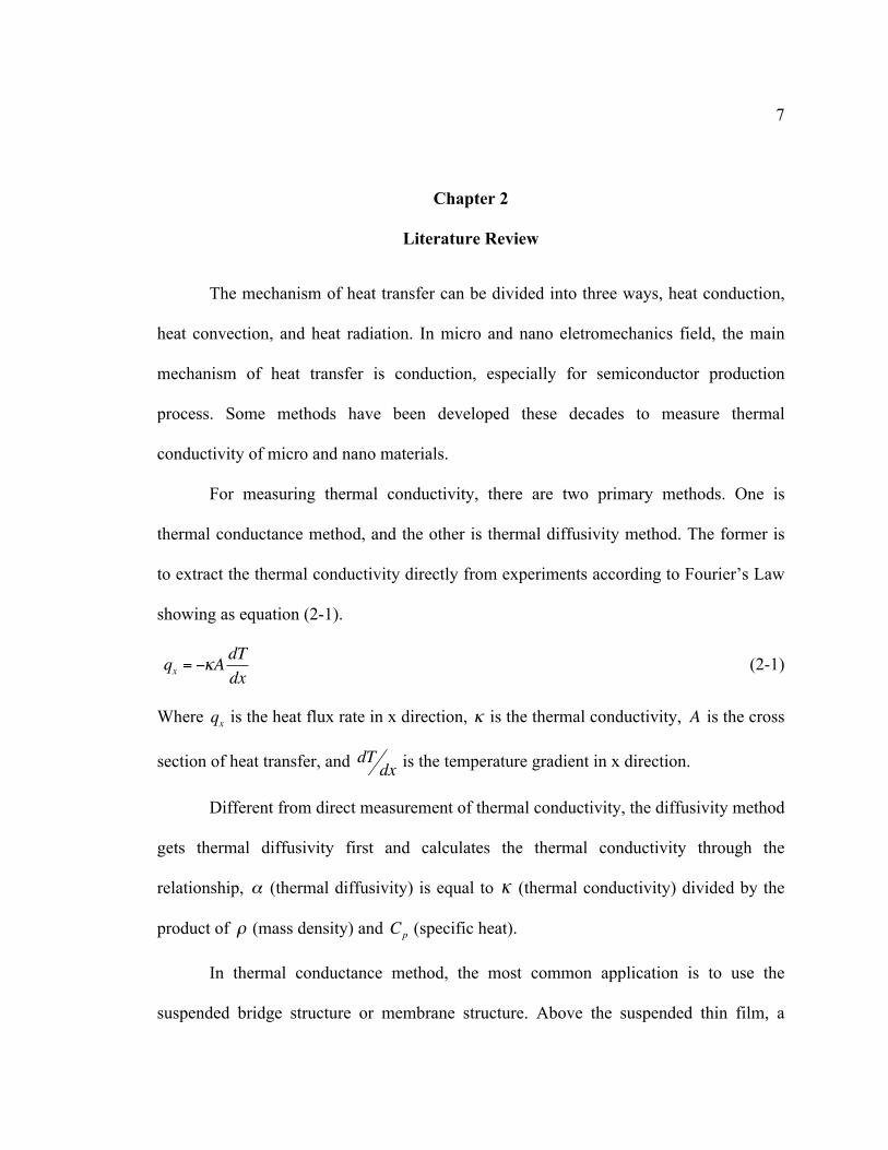
Chapter 2
Literature Review
The mechanism of heat transfer can be divided into three ways, heat conduction,
heat convection, and heat radiation. In micro and nano eletromechanics field, the main
mechanism of heat transfer is conduction, especially for semiconductor production
process. Some methods have been developed these decades to measure thermal
conductivity of micro and nano materials.
For measuring thermal conductivity, there are two primary methods. One is
thermal conductance method, and the other is thermal diffusivity method. The former is
to extract the thermal conductivity directly from experiments according to Fourier’s Law
showing as equation (2-1).
!
qx = "#AdT
dx (2-1)
Where
!
qx is the heat flux rate in x direction,
!
" is the thermal conductivity,
!
A is the cross
section of heat transfer, and
!
dTdx
is the temperature gradient in x direction.
Different from direct measurement of thermal conductivity, the diffusivity method
gets thermal diffusivity first and calculates the thermal conductivity through the
relationship,
!
" (thermal diffusivity) is equal to
!
" (thermal conductivity) divided by the
product of
!
" (mass density) and
!
Cp (specific heat).
In thermal conductance method, the most common application is to use the
suspended bridge structure or membrane structure. Above the suspended thin film, a

8
heater and a thermal sensor are deposited to measure the in-plane thermal conductivity.
McConnell et al. [1] used this method to measure the thermal conductivity of poly-silicon
film, and Figure 2-1 shows the suspended device. When DC current is passing through
the heater in the middle of the structure, heat flow is produced because of Joule heating.
The resistance of thermometer varies with change of temperature. According to Fourier’s
Law, the thermal conductivity can be calculated by equation (2-2).
Figure 2-1: Measurement structure schematic proposed by McConnel [1]
!
" =(Q /2)(Xthermometer # Xheater )
Ac (Theater #Tthermometer) (2-2)
2.1 Thermal Conductivity Measurement by 3! method
An important technology, 3! method, is one kind of thermal conductance
methods with the easy-applied and high-accurate characteristics. It can measure thermal

9
properties of several different structures of micro or nano materials. The solid sample
geometry in 3! method can be divided into three types, Line Heater on Substrate, Thin
Film on Substrate, and Suspended Wire. The measurement applications of 3! method are
introduced by the following paragraphs according to different geometry catalogs.
2.1.1 Line Heater on Substrate
To measure thermal conductivity of bulk materials in 3! technique, the bulk
sample is prepared adjacent to a patterned strip metal film which is shown as Figure 2-2.
The strip metal film acts both as a thermometer and a line heater driven by a periodically
oscillating (1!) heat source. The heat causes temperature oscillations of line heater at 2!,
and the temperature oscillations make the resistance of line heater varying at 2!.
Therefore, voltage oscillations at 3! can be derived. The thermal conductivity
information of the underlying sample can be extracted from the amplitude of voltage
oscillations of the line heater.
Figure 2-2: Side view of geometry of line heater on substrate
Cahill [2] utilized 3! method to measuring the thermal conductivity of
amorphous solids in the temperature range between 30K to 300K. A four-probe

10
configuration of metal line heater on top of sample substrate was proposed as shown in
Figure 2-3. The outside two electrode pads were used to feed in the periodically
oscillating heat source (a.c. constant current source), and the inside two pads are for
measuring the voltage drop across the line heater. The temperature oscillation of line
heater and the thermal conductivity of sample can be calculated from 1! voltage and 3!
voltage of the line heater.
Figure 2-3: Four pads patterned metal film on amorphous substrate [2]
In 1990, Cahill [3] published thermal conductivity measurement with temperature
range from 30K to 750K. Equation (2-3) presents calculation of temperature oscillation,
and equation (2-4) shows the governing equation of thermal conductivity.
(2-3)
(2-4)
The wave penetration depth (WPD) means the wavelength of diffusive thermal
wave and is defined as Equation (2-5). D presents the thermal diffusivity of line heater,
!
"T = 4dT
dRRV3#
V1#
!
" s =
V1#3ln(
f2
f1)
4$LR2(V3# ,1 %V3# ,2)&dR
dT

11
and ! is the frequency of heat source (a.c. current source). If WPD is much smaller than
sample thickness, the semi-infinite substrate condition can be assumed. The proper
operating frequency of heat source also can be decided by the assumption: WPD is much
larger than line heater width.
!
WPD =D
2" (2-5)
2.1.2 Thin Film on Substrate
Cahill [4] proposed thermal conductivity measurements of a-Si:H thin film on
substrate. The sample was deposited on a substrate as a thin layer on the order of 100µm.
Then, a strip of metal was added on the top of sample film, and it acted as a line heater
and also a thermal sensor. Four electrode pads were using to feed in the a.c. constant
current and measure the voltage drop as shown in Figure 2-4. The rule here is that the
width of the metal strip must be at least five times larger than the thickness of sample
film, then the heat transfer can be viewed as one dimension (cross-plane) problem.
Figure 2-4: Geometry of the thin file thermal conductivity measurement [4]

12
If the thermal conductivity of thin film is small compared to the thermal
conductivity of substrate, and WPD is much larger than the thickness of thin film at low
frequency. Then, the temperature oscillation of the thin film can be shown as equation (2-
6), which is independent of frequency. Pl is the unit power density of the line heater, and t
is the thickness of thin film. 2b stands for the width of line heater. The temperature at
substrate is shown as equation (2-7).
!
"Tf =Plt
# f 2b (2-6)
!
"Ts =Pl
#$ s
sin2(kb)
(kb)2(k
2+ q
2)1/ 2dk , q
2=
0
%
&1
WPD2
=2'
D (2-7)
Wang et al. [5] measured not only thermal conductivity of the SiO2 thin film but
also the thermal conductivity of Si substrate by extending 3! method to wide-frequency
range. Figure 2-5 shows temperature oscillation results.
Figure 2-5: The real part of temperature oscillation as function of frequency [5]

13
A practical extended 3! method has been proposed to measure thermal
conductivity and thermal diffusivity of multilayer structures by B. W. Olson et al. [6].
The two-layer structure is shown as Figure 2-6. Part (a) in Figure 2-6 is the 3! line
element, and part (b) is the plane view of it. Figure 2-7 presents how the width of 3! line
element can affect the heat flow path.
Figure 2-6: A two-layer structure of 3! applications [6]
Figure 2-7: (a) a thin line (b) a wide line [6]
There are two samples measured in this research. The first two-layer sample is
composted of a borosilicate glass substrate, a consolidated zeolite film, and a copper line
heater. The other one is made of a bulk silicon substrate, a SiO2 thermal oxide film, and a
aluminum line heater. Thermal conductivities and thermal diffusivities of substrates and
films are all measured by 3! method.

14
2.1.3 Suspended Wire
Lu et al. [7] measured thermal conductivity of a filament-like specimen with four-
probe configuration by applying 3! method. The measurement schematic is shown in
Figure 2-8. The specimen of this method restricts to be electrically conductive, and the
resistance of the specimen should vary with temperature. The a.c. constant current (1!) is
fed in from the outside two probes, and the three omega voltage (V3!) is obtained from
the inside two probes. V3! can be derived from the heat generation and diffusion equation
(2-8) and boundary conditions (2-9). The value of V3! is approximately proportional to
the dimensions of the specimen, shown as equation (2-10). Once V3! is obtained from
experiments, the thermal conductivity can be back calculated. This research measured
thermal conductivity and specific heat of the platinum wire and multiwall carbon
nanotube bundles. In addition, the amplitude of current is restricted in suspended wire
configuration shown as equation (2-11).
Figure 2-8: Illustration of the four-probe configuration of a filament-like specimen [7]
!
"Cp
#
#tT(x,t) $%
# 2
#x2
T(x, t) =I02sin
2&t
LS[R + ' R (T(x, t) $T0)] (2-8)

15
where Cp, ", R, and # are the specific heat, thermal conductivity, electrical resistance, and
mass density of the specimen at the substrate temperature T0.
Boundary conditions,
!
T(0,t) = T0
T(L,t) = T0
T(x,"#) = T0
$
% &
' &
(2-9)
!
V3" #
4I3$
e$e%
& 4' 1+ (2"()2L
S
)
* + ,
- .
3
(2-10)
where #e is the electrical resistivity of the specimen, and S is the cross section of the
specimen.
!
I0
2 " R L
n2# 2$S
<<1 (2-11)
Dames and Chen [8] used the voltage source to approximate a.c. current source as
shown in Figure 2-9. They added DC offset to the heat source, therefore V0! and V2! can
be obtained besides V1! and V3!. Figure 2-10 compares the traditional and DC-offset
added 3! method. The voltage from measurement can be divided into in-phase (real) part
X and out-of-phase (imaginary) part Y shown as equation (2-12).
Figure 2-9: Circuits of voltage approximated current source [8]

16
Figure 2-10: Schematic of traditional and DC offset added 3! method [8]
!
Vn" ,rms
2#Re0
2I1,rms
3= Xn ("1,$) + jYn ("1,$) (2-12)
The important result of this paper is the summary of relationship between (in-
phase and out-of-phase) electrical transfer functions and thermal transfer function Z
shown as Figure 2-11.
Figure 2-11: Relationship between electrical and thermal functions [8]

17
Thermal conductivity measurement of a non-electrical conducting suspended wire
can also be implemented by 3! method. O. Bourgeois et al. [9] patterned a NbN
thermometer on top of Si nanowire and utilized suspended wire configuration 3! method.
The individual single-crystalline silicon nanowires are fabricated by e-beam lithography
and suspended between two separated SiO2 pads as shown in Figure 2-12. These
experiments are executed at low temperature around 0K$ 2K and at low frequency
around 0Hz $ 50Hz. The results of experiments showed that the conductance behaves as
T3 as shown in Figure 2-13.
Figure 2-12: The image of suspended silicon nanowire and the schematic of this device [9]

18
Figure 2-13: Relationship between thermal conductance and temperature [9]
2.2 Strain Effects on Thermal Conductivity
Generally, thermal conductivity of a solid can be contributed from transports of
phonons and electrons. At microscale and nanoscale limits, the classic model of heat
conduction is inadequate for predicting thermal conductivity. There are two primary
approaches applied on the new models used for predicting the thermal conductivity of the
microscale and nanoscale devices. One is Boltzmann transport equation (BTE) which
describes the statistical distribution of particles in a fluid. It is used to study how a fluid
transports physical quantities (such as heat and charge), then some transport properties
(such as electrical conductivity, hall conductivity, viscosity, and thermal conductivity)
can be derived. The other approach is Molecular dynamics (MD). It is a form of
computer simulation wherein atoms and molecules are allowed to interact for a period of
time under known laws of physics, which gives a view of the motion of the atoms.
There are two distinct types of parameters control effective thermal conductivity.
The first type is thermodynamic parameters, such as temperature and pressure. The other

19
one is extrinsic parameters, such as impurities, defects, and bounding surfaces. Nanoscale
devices, particularly thin film, usually contain residual strain after fabrication, which may
considerably affect the thermal transport properties of the material and the device
concerned. The effect of strain (tri-axial strain equivalent to the uniform pressure) on
thermal conductivity is still an unexplored research field. Bhowmick and Shenoy [10]
studied effect of strain on thermal conductivity of insulating solids. In this study, the
thermal current was carried solely by phonons due to insulating solids. They performed
classical molecular dynamics simulations and obtained the strain and temperature
dependence on thermal conductivity. In addition, they changed the velocity of sound and
relaxation time of phonons to observe how strain affects thermal conductivity. Figure 2-
14 shows the relationship among thermal conductivity, temperature, and strain.
Figure 2-14: Thermal conductivity as a function of temperature and strain [10]
Tamma et al [11] discussed mechanical strain effect on thermal conductivity of
single-wall carbon nanotubes. Compression, tension, and torsion were applied to SWNT
in this study. They found that thermal conductivity didn’t change much for small strained

20
tube. However, the bulking collapse reduced the thermal conductivity in a compressed
and torsionally twisted tube. In tensile stretched case, no significant result was found. The
result in detail is shown in Figure 2-15.
Figure 2-15: Thermal conductivity and mechanical strains [11]

21
2.3 Reference
[1] A. D. McConnell, S. Uma, and K. E. Goodson, “Thermal Conductivity of Doped
Polysilicon Layers”, J. Microelectromechanical Sys. 10(3), September 2001, p.360~369
[2] D. G. Cahill and R. O. Pohl, “Thermal Conductivity of amorphous solids above
the plateau”, Phys. Rev. B 35(8), March 1987, p.4067~4073
[3] D. G. Cahill, “Thermal Conductivity measurement from 30 to 750K: the 3!
method”, Rev. Sci. Instrum. 61(2), February 1990, p.802~808
[4] D. G. Cahill, M. Katiyar, and J. R. Abelson, “Thermal conductivity of a-Si:H thin
films”, Phys. Rev. 50(9), September 1994, p.6077~6081
[5] Zhao Liang Wang, Da Wei Tang, and Xing Hua Zheng, “Simultaneous
determination of thermal conductivities of thin film and substrate by extending 3!-
method to wide-frequency range”, Appl. Surface Sci. 253, May 200, p.9024~9029
[6] B. W. Olson, S. Graham, and K. Chen, “A pratical extension of 3! method to
multilayer structures”, Rev. Sci. Instrum. 76(5), April 2005
[7] L. Lu, W. Yi, and D. L. Zhang, “3! method for specific heat and thermal
conductivity measurements”, Rev. Sci. Instrum. 72(7), July 2001, p.2996~3003
[8] C. Dames and G. Chen, “1!, 2!, and 3! methods for measurements of thermal
properties”, Rev. Sci. Instrum. 76(12), December 2005
[9] O. Bourgeois, T. Fournier, and J. Chaussy, “Measurement of the thermal
conductance of silicon nanowires at a low temperature”, J. Appl. Phys. 101(1), January
2007

22
[10] S. Bhowmick and V. B. Shenoy, “Effect of strain on the thermal conductivity of
solids”, J. Chem. Phys. 125, October 2006
[11] C. Anderson, K. K. Tamma, and D. Srivastava, “Prediction of thermal
conductivity of single-wall carbon nanotubes with mechanical strains”, AIAA 2004-819

23
Chapter 3
Analytic Modeling of 3! Method
3.1 Introduction of 3! Method
3! method is a commonly used and easily applied technique to measure thermal
properties of bulk materials, thin films, wires, and liquid as well. Generally, the sample
preparation is limited to a patterned conducting line film deposited on top of the sample.
The conducting film serves as both a heater and a sensor, and it is called line heater. The
main principal of 3! method shows as Figure 3-1.
Figure 3-1: Principal of 3! method
3! method utilizes periodically oscillating current source with 1! frequency to
drive the line heater to generate joule heating at 0! and 2! frequency. Then, heating
leads to temperature fluctuation at 0! and 2! frequency. The temperature difference
causes resistance variation of heater at 0! and 2! frequency. Eventually, the voltage of
heater is equal to current multiplied by resistance, and it contains 1! and 3! components.

24
The thermal information that we are interested can be extracted from 3! voltage. Figure
3-2 explains the concept of 3! method.
Figure 3-2: 3! method
There are several kinds of geometry of sample preparation for 3! method. For
line-heater-on-substrate, thin-film-on-substrate, and multilayered-thin-film-on-substrate,
there is a metal line deposited on the sample to act as the heating source and sensing
element. Thermal conductivities of these thin films and substrate can be revealed by 3!
method. Another geometry called suspended-wire, and this freestanding wire is not only
the heater but also the sensor. 3! method is utilized to measure the thermal properties of
the freestanding wire instead of thermal property of substrate.
However, the fabrication technique to make freestanding films at nanoscale is still
a challenge. Therefore, this study deposits the nano-/micro-wire on top of the substrate
instead of suspended wire. In this wire-on-substrate geometry, the heat diffused to the

25
substrate needs to be considered. The main object of this study is to verify the 1-D heat
conduction model by considering heat loss into substrate and to get thermal conductivity
of the nano-/micro-wire from the third harmonic voltage information. The following
sections start from the continuity equation to heat conduction equation and reveal the
modeling of wire-on-substrate.
3.2 Continuity Equation
The conservative transport of energy can be described by the continuity equation.
The divergence of flux density is equal to the negative rate change of energy density with
no generation or removal rate of energy, as shown in equation (3-1).
!
" • J = #$%energy
$t (3-1)
For one-dimensional heat conducting, J means heat flux density (W/m2) and
presents as equation (3-2). #energy stands for heat density (J/m3), and %(x,t) is temperature
difference.
!
J = "#$% = "#&%(x, t)
&x (3-2)
!
" • J =" • (#$%&(x, t)
%x) = #$
% 2&(x, t)
%x 2 (3-3)
!
"#energy
"t="(#Cp$(x, t))
"t= #Cp
"$(x,t)
"t (3-4)
Therefore, the one-dimensional heat conduction equation without any heat source
or sink can be derived as equation (3-5).

26
!
"Cp
#$(x,t)
#t=%
# 2$(x,t)
#x 2 (3-5)
!
" :mass density
Cp : specific heat
# : thermal conductivity
$
% &
' &
(
) &
* &
3.3 1-D Heat Conduction Equation with Heat Source
In 3! method, a periodically oscillating heat source (I=I0sin!t) is applied to a
metal wire and leads to joule heating which is equal to I2(R0+&R). &R means the
resistance fluctuation of the metal wire and is proportional to temperature difference. The
one-dimensional heat conduction equation of freestanding wire with heat source is
showing as equation (3-6). L and S are the length and the cross-section of metal wire, and
!
" R is resistance derivative of temperature.
!
"Cp
#$(x,t)
#t=%
# 2$(x,t)
#x2
+I02sin
2&t
LS(R0 + ' R $(x, t)) (3-6)
3.4 1-D Heat Conduction Equation with Heat Source and Heat Sink
Before calculating the heat loss to substrate, we need to define the temperature
profile along y direction that points into the substrate as shown in Figure 3-3. We assume
temperature of the surface of substrate is the same as temperature of the nanostructure
and ignore the interface resistance. In addition, the temperature change of our sample
along the longitudinal direction can be viewed as . Then, difference of temperature
decays exponentially along y direction and the temperature profile can be viewed as

27
!
"(x, t)e#y
$ . The parameter of exponential term relates to thermal wave penetration depth '
which is equal to
!
"s
2#. (s is thermal diffusivity of substrate, and ! is frequency of
heat source.
Figure 3-3: Geometry of wire-on-substrate
The heat flux through the interface (y=0) from wire to substrate is shown as
equation (3-7). "s is thermal conductivity of substrate, and A is contacting area between
wire and substrate.
Y
X
Y
L
Substrate
Sample

28
!
qA y= 0=" sA
#($(x,t)e%y
& )
#yy= 0
=" sA[%1
&$(x, t)e
%y
& ]
y= 0
= %" sA$(x, t)
& (3-7)
Therefore, the 1-D heat conduction equation of wire-on-substrate model can be
derived as equation (3-8).
!
"Cp
#$(x,t)
#t=%
# 2$(x,t)
#x2
+I02sin
2&t
LS(R0 + ' R $(x, t)) (
% sA
LS)$(x, t) (3-8)
3.5 Solution of 1-D Heat Conduction Equation with Heat Source and Heat Sink
From equation (3-8), we can get
!
"#(x, t)
"t$
%
&Cp
" 2#(x,t)
"x2
$ (I02sin
2't ( R
LS&Cp
$% sA
LS)&Cp
)#(x,t) =I02R0
LS&Cp
sin2't (3-9)
!
"#$(x, t)
#t% A
# 2$(x, t)
#x 2% (Bsin
2&t %C)$(x, t) = Dsin2&t (3-10)
!
A ="
#Cp
B =I0
2 $ R
LS#Cp
C =" sA
LS%#Cp
D =I0
2R0
LS#Cp
&
'
( ( ( (
)
( ( ( (
Boundary conditions and initial condition are shown as following.
!
"(0,t) = 0
"(L,t) = 0
"(x,#$) = 0
%
& '
( '
(3-11)

29
Equation (3-10) shows a non-homogenous PDE equation. We use impulse
theorem to modify it to be a homogenous PDE equation. Let
!
z(x," +) = Dsin
2#" and
!
"(x, t) = z(x, t;#)d#$%
t
& . We can get
!
"z
"t# A
" 2z
"x 2# (Bsin
2$t #C)z = 0 (3-12)
!
z(0,t) = 0
z(L,t) = 0
z(x," +) = Dsin
2#"
$
% &
' &
(3-13)
From boundary condition, we can assume
!
z(x, t;") = Un(t;")sin
n#x
Ln
$ (3-14)
Substitute equation (3-14) into equation (3-12)
!
dUn
dt+ (A
n2" 2
L2# Bsin2$t + C)U
n
%
& '
(
) * sin
n"x
L= 0
n
+ (3-15)
For non-trivial solution of equation (3-15)
!
dUn
dt+ (A
n2" 2
L2# Bsin
2$t + C)Un
= 0 (3-16)
When
!
B << An2" 2
L2
+ C #I0
2 $ R L%
n2" 2&%S +&
sLA
<<1, equation (3-16) becomes
!
dUn
dt+ (A
n2" 2
L2
+ C)Un
= 0 (3-17)
!
"Un(t;# ) = E
ne$(A
n2% 2
L2
+C )( t$# )
(3-18)
!
" Zn(x, t;#) = E
ne$(A
n2% 2
L2
+C )( t$# )
n
& sinn%x
L (3-19)

30
From initial condition, we know
!
Zn(x," +
) = En
n
# sinn$x
L= Dsin
2%" (3-20)
!
" En
= D #2
Lsin
2$% sinn&x
Ldx =
2D
n&[1' ('1)n ]sin2$%
0
L
( (3-21)
!
" z(x, t;#) =2D
n$[1% (%1)n ]sin2&#e
%(An2$ 2
L2
+C )( t%# )
sinn$x
Ln
' (3-22)
Now, let’s find out
!
"(x, t)
!
"(x, t) = z(x, t;#)d#$%
t
& =2D
n'[1$ ($1)n ]sin
n'x
Le$(A
n2' 2
L2
+C )t
e(A
n2' 2
L2
+C )#
$%
t
& sin2(#d#
)
* + +
,
- . .
/
0 1
2 1
3
4 1
5 1 n
6
(3-23)
Let
!
G = An2" 2
L2
+ C , and solve equation (3-23)
!
"(x, t) =2D
n#[1$ ($1)n ]sin
n#x
L
1
G
G2
+ 4% 2 $Gcos(2%t) + 2%Gsin(2%t)
2(G2
+ 4% 2)
&
' (
)
* +
n
,
=D
n#[1$ ($1)n ]sin
n#x
L
1
G1$
G2cos(2%t) + 2%Gsin(2%t)
G2
+ 4% 2
&
' (
)
* +
n
, (3-24)
Let
!
sin" =G
G2
+ 4# 2
cos" =2#
G2
+ 4# 2
$
% & &
' & &
(3-25)
!
"(x, t) =D
n#[1$ ($1)n ]sin
n#x
L
1
G1$
G
G2
+ 4% 2sin& cos(2%t) + cos& sin(2%t)
'
( )
*
+ ,
n
- (3-26)
!
"#(x, t) =D
n$[1% (%1)n ]sin
n$x
L
1
G1% sin& sin(2't + &)[ ]
n
( (3-27)
!
sin" =1
1+ cot2 "

31
!
"#(x, t) =D
n$[1% (%1)n ]sin
n$x
L
1
G1%sin(2&t + ')
1+ cot2 '
(
) * *
+
, - - n
. (3-28)
Take n=1, the temperature difference becomes as equation (3-29)
!
"(x, t) =2D
#sin
#x
L
1
G1$sin(2%t + &)
1+ cot2 &
'
( ) )
*
+ , , (3-29)
Then, resistance variation can be obtained like equation (3-30)
!
"R =# R
L$(x, t)dx =
4D # R
% 2G1&sin(2't + ()
1+ cot2 (
)
* + +
,
- . . 0
L
/ (3-30)
The voltage of wire is showing as equation (3-31)
!
V (t) = I0 sin"t R +4D # R
$ 2G1%sin(2"t + &)
1+ cot2 &
'
( ) )
*
+ , ,
-
. /
0 /
1
2 /
3 / (3-31)
Because of
!
sin(2"t + #)sin"t = $1
2[cos(3"t + #) $ cos("t + #)]
and
!
1
1+ cot2 "
=G
G2
+ 4# 2=
1
1+ 4# 2G2
Therefore,
!
V (t) = I0R +4I0 " R D
# 2G
$
% &
'
( ) sin*t +
2I0 " R D
# 2G
1
1+ 4* 2G2cos(*t + +)
+2I0 " R D
# 2G
1
1+ 4* 2G2cos(3*t + +)
(3-32)
If
!
4" 2<<G
2 # 2" <<$
%Cp
& 2
L2
+1
%Cp
$ sA
LS'
(
) * *
+
, - - , the magnitude of 3! voltage becomes
!
V3" ,rms
#4I
rms
3R0$ R L
% 4&S +L% 2&
sA
'
(3-33)

32
!
!sin" =G
G2
+ 4# 2$" = sin
%1 G
G2
+ 4# 2
&
' (
)
* +
&G2
>> 4# 2
," - sin%1(1) =.
2
Therefore, the magnitude of 1! voltage is
!
V1" ,rms
# 2Irms
R0
+12I
rms
3R0$ R L
% 4&S +L% 2&
sA
'
(3-34)
The average temperature change of the wire can be calculated from equation (3-29)
!
" #8I
rms
2R0L
$ 4%S +L$ 2%
sA
&
(3-35)
Therefore, the thermal conductivity of wire can be derived from equation (3-33)
!
" #
4Irms
3R0$ R L
V3%
&L' 2"
sA
(
)
* +
,
- .
' 4S
(3-36)
3.6 Reference
[1] L. Lu, W. Yi, and D. L. Zhang, “3! method for specific heat and thermal
conductivity measurements”, Rev. Sci. Instrum. 72(7), July 2001, p.2996~3003
[2] Z. L. Wang et al, “Length-dependent thermal conductivity of an individual single-
wall carbon nanotube”, Appl. Phys. Letters 91, 2007, p.123119

33
Chapter 4
Experimental Method
This chapter introduces the sample preparation and experimental set-up of 3!
method.
4.1 Sample Preparation
In this study, we utilize 3! technique to measure thermal conductivity of metal
thin films and nanoscale semiconductors. The metal used is evaporated aluminum, which
is 99.99% pure evaporated aluminum of glass substrate and subsequently patterned using
photo-lithography and wet etching. The mean grain size of the 130-150 nm thick
specimens is about 50 nm as obtained by transmission electron microscopy. Figure 4-1
shows scanning electron microscope (SEM) image of our aluminum specimen with the
dimensions of 100"m long, 10" wide, and 130nm thick. In addition, we also have a
focused-ion-beam deposited platinum nanowire across lithographically patterned gold
electrodes on substrate. The substrate is a commercially available silicon wafer with
about 500 nm thick thermally grown oxide layer at the top. The FIB Pt specimen is 7µm
long, 600nm wide, and 800nm thick showing as Figure 4-2.

34
Figure 4-1: SEM image of aluminum specimen
Figure 4-2: Schematic of 3! technique applied on FIB-deposited Platinum
Electrodes
Electrodes
Aluminum thin film
A
B
Reference in
SR830
Lock-in Amp
Phase marker
KEITHLEY
6221
FIB Pt nanowire sample
10µm

35
4.2 Experimental Set-up
Figure 4-2 shows the experimental setup schematic along with a scanning electron
micrograph of a focused-ion-beam deposited platinum nanowire across lithographically
patterned gold electrodes. For conducting nanowires, the parasitic/contact resistances
usually are of the same magnitude as the measured DUT (device-under-test) resistance.
Therefore, the electrodes with four-probe configuration are used to eliminate contact
resistance and minimize experimental error of measurement. The experiments are
performed in vacuum environment to prevent heat loss through convection. The main
components of the experimental setup are the Keithley 6221 constant current source and
the Stanford SR830 lock-in amplifier [1].
4.2.1 Main Apparatus
The power supply, Keithley 6221 constant current source, has periodical wave
output function. It’s utilized to provide a constant alternating current I0sin!t through the
specimen. The phase marker function of Keithley 6221 allows user to set a pulse marker
that defines a specific point of a waveform over a range of 0 to 360°. The phase marker
signal is a 1"s pulse that appears on the selected line of the external trigger connector.
Then, we use this external trigger signal inputs into the lock-in amplifier as a reference of
frequency detection.
The Stanford SR830 lock-in amplifier is proficient for measuring small a.c.
signals that can reach nano-volt levels with a very low level of noise floor. It has the
reference in function that can recognize the specific frequency which users are interested

36
in, and it can measure not only voltage but also current signal at this specific frequency
and it’s harmonics. There are single and differential input models in SR830 lock-in
amplifier. The differential input method is utilized in this study to eliminate common
mode noise signal.
The key features of a 3! experiment are the choice of amplitude of the a.c.
current, the low frequency operating settings of the lock-in amplifier, and use of a high
vacuum environment. From the analytical model we recognize a current limitation:
!
I0
2 " R L#
n2$ 2%#S +%
sLA
<<1 implicit in the derivation of
!
"(x,t) . Therefore, the amplitude of the
applied current can’t be too large. However, from a measurement stand-point it has to be
large enough so that the signal to noise ratio of the 3! signal is satisfactory.
The most important parameter in using the lock-in amplifier is the time constant
which decides the bandwidth of low pass filter. For example, we use 30~300 seconds
here for the frequency range of a.c. current from 30Hz to 1Hz to fulfill the frequency
limitation:
!
2" <<#
$Cp
% 2
L2
+1
$Cp
# sA
LS&
'
( ) )
*
+ , , .
4.2.2 Cryogenic Station
The 3! experiments are performed in a cryogenic station at a high vacuum
environment to prevent heat convection losses. This cryogenic station as showing in
Figure 4-3 is a digital Deep Level Transient Spectroscopy (DLTS) system that can
provide the environment temperature between 50F ~ 300F.

37
Figure 4-3: Experimental set-up of 3! technique
4.3 Calibration
One of these traditional 3! geometries, line heater on substrate, is utilized to
calibrate our experimental setting. The metallic material of line heater is silver thin film
patterned to be 100µm long, 20µm wide, and 200nm thick, and the sample is glass
substrate. The thermal conductivity value of glass from literature is 1.1mW/K. Cahill’s
model showing as equation (4-1) is used to obtain thermal conductivity of glass substrate.
Figure 4-4 shows the measured 3! voltage, then we can derive the thermal conductivity
value of glass substrate from these data. Thermal conductivity value is equal to
1.07mW/K, and the error is about 2.7%.

38
!
" s =
V1#3lnf2
f1
4$lR2(V3# ,1 %V3# ,2 )
dR
dT (4-1)
Where,
!
V1" is the voltage across the metal strip at frequency !,
!
V3" ,1 and
!
V3" ,2 are the
voltages at the third harmonic for frequency f1 and f2 respectively, R and l are the metal
line resistance and length respectively, and R) is the slope of resistance as a function of
temperature at the temperature of measurement.
Figure 4-4: 3! voltage measurement by using silver line heater on glass substrate sample geometry
4.4 Reference
[1] T. Y. Choi et al, “Measurement of thermal conductivity of individual multiwalled
carbon nanotubes by the 3-! method”, Appl. Phys. Letters 87, 2005, p.013108

39
Chapter 5
Results and Discussion
The new 3! model developed in this study is first experimentally characterized
and calibrated on a metal specimen of known thermal conductivity. The metal used is
evaporated aluminum that is lithographically patterned with four electrodes to present
four-configuration measurement. The following section shows our results of thermal
conductivity of aluminum agreed with the literature value nicely. Afterward, our 3!
model is utilized to measure thermal conductivity of focused ion beam deposited
platinum nanowire without releasing it from substrate. Then, following by the conclusion.
5.1 Aluminum Film
According to our 3! analytic model, the thermal conductivity of sample can be
extracted from the 3! voltage by using equation (5-1). For eliminate the measuring error,
we first use measured data of 3! voltage to fit into the traditional 3! model, Cahill’s
line-heater-on-substrate model showing like equation (5-2), to obtain the "s (thermal
conductivity of substrate). Then, substitute the derived value of "s and measured data of
3! voltage into our 3! model to obtain thermal conductivity of our aluminum thin film
sample.
!
V3" ,rms
#4I
rms
3R0$ R L
% 4&S +L% 2&
sA
'
(5-1)

40
!
" s =
V1#3lnf2
f1
4$lR2(V3# ,1 %V3# ,2 )
dR
dT (5-2)
5.1.1 Temperature Dependence of Resistance of Aluminum Film
The parameter, R), needs to be known before executing this model. R) is the slope
of resistance of the sample as a function of temperature at the temperature of
measurement, and we can measure it by performing four-point resistance measurement
and using the cryogenic station. Figure 5-1 shows that
!
dR
dT is equal to 0.0086 #/K.
Figure 5-1: Temperature dependence of resistance of aluminum film

41
5.1.2 Measurement of Thermal Conductivity
The aluminum thin film sample reported here is lithographically patterned to be
150µm long, 10µm wide, and 130nm thick. Figure 5-2, Series 1 presents the measured
rms value of 3! voltages in the frequency range 1 Hz ~ 30Hz which matches well with
the expected data, based on the analytical model, showing as Series 2. The difference
between measured data and expected data is showing as Series 3 in Figure 5-2. We
observe that the 3! voltages slightly increase with a decrease in the frequency, which is a
reasonable result because the 3! voltages are related to thermal penetration depth '
according to equation (5-1). We fit this data to the Cahill’s model, i.e. equation (5-2), to
find out the thermal conductivity of glass substrate, resulting in a value of 1.07 W/mK at
297K. This result matches the value gotten from our calibration experiment. By
substituting this value of thermal conductivity of the glass substrate into our 3! model,
i.e. equation (5-1), we obtain the thermal conductivity of the aluminum thin film as
shown in Figure 5-3.
Additionally, according to our model equation (5-1) implies a linear relationship
between 3! voltage (
!
V3" ) and cube of the current amplitude (
!
I0
3), and this is
experimentally verified and graphically shown in Figure 5-4. Here we chose the value of
0.003 amp as the amplitude of a.c current in order to fulfill the current limitation criteria,
!
I0
2 " R L#
n2$ 2%#S +%
sLA
<<1.

42
Figure 5-5 shows the length dependence of thermal conductivity of aluminum thin
film with the same width. The result presents there is no obvious variance at thermal
conductivity of aluminum films with the micro-length scale.
Figure 5-2: The measured
!
V3" and expected
!
V3" of aluminum thin film

43
Figure 5-3: Thermal conductivity of aluminum thin film
Figure 5-4: The proportional relationship between
!
V3" of aluminum thin film and
!
I0
3

44
Figure 5-5: The length dependence on thermal conductivity of aluminum thin film
5.2 Focused Ion Beam Deposited Platinum Nanowire
After verifying the analytical model and calibrating the experimental setup, the
experiments on FIB-deposited platinum nanowires are performed. The specimen is 7µm
long, 600nm wide, and 800nm thick. The resistance of FIB platinum is measured by I-V
measurement and showing as Figure 5-6. The chemical composition of FIB platinum
shows like Figure 5-7. Carbon (45%~55%) and platinum (40%~50%) are the major
components [1]. Therefore, we can expect the behavior of temperature dependence of
resistance of FIB platinum acts like semiconductors showing as Figure 5-8.

45
Figure 5-6: Resistance of FIB platinum
Figure 5-7: Components of FIB platinum

46
Figure 5-8: Temperature dependence of resistance of FIB platinum
Figure 5-9 and Figure 5-10 individually show the
!
V3" value and average
temperature change measured experimentally. The amplitude of a.c. current and the
operating frequency used here are 7.07 µA and 1000Hz~400Hz, which satisfies the
restrictions built into the analytical 3! model. The value of thermal conductivity of FIB
platinum nanowire obtained from measurement is 40.97W/mK at room temperature. For
pure platinum, the thermal conductivity is 71.6W/mK at room temperature. The variation
seen is because the FIB-deposited Pt is not just purely Pt metal, but is a conducting
metal-organic polymer (C9H16Pt) which in its as-deposited form creates a nanostructure
made of Pt and amorphous carbon mixture (The Ga+ ion in the ion beam causes
amorphization of the carbon). The thermal conductivity of amorphous carbon varies from
0.3 to 10W/mK at room temperature. If we use a simple rule of mixtures like equation

47
using 50% platinum contribution and 50% amorphous carbon contribution, we obtain an
approximated thermal conductivity value of FIB-deposited platinum to be about
40.8W/mK that matches our data very well. The measured value of thermal conductivity
of FIB-deposited platinum nanowire is found to be in within the expected bounds. In
addition, let’s take a look at equation (5-1), the denominator of amplitude of
!
V3" includes
two terms,
!
" 4#S and
!
L" 2#sA
$. In our case, the order of
!
" 4#S is 10-8
, and the order of
!
L" 2#sA
$ is 10
-11. This means that
!
" 4#S is much larger than
!
L" 2#sA
$, and thus
!
L" 2#sA
$,
which represents the heat loss from FIB platinum nanowire to substrate is very small in
this case, and can be neglected, which concurs with one of the starting assumptions of the
analytical model.
Figure 5-9: The measured
!
V3" for FIB-deposited Pt nanowire

48
Figure 5-10: The average temperature change of FIB Pt nanowire
5.3 Conclusion
We have developed a model that allows the 3! technique to measure in-plane
thermal conductivity of specimens that are not necessarily released from the substrate, as
required by the conventional scheme. Figure 5-11 shows the conventional 3!
experimental setup, where an electrically conductive strip is connected to four electrodes.
For insulating specimens (Figure 5-11a), the substrate is the specimen and the top layer is
the metal film that is used as a heater and a temperature sensor. Generally, to measure the
in-plane thermal conductivity, the specimen must be released from the substrate (as
Figure 5-11b), and the experiments are conducted in vacuum to prevent heat losses. The

49
in-plane thermal conductivity is obtained from the third harmonic voltage signal (
!
V3" )
using the following expression,
3
24
3
0
3
)2(1
4!"
#$%
&
+
'(
S
LIV
ee
)*+,
--) (5-3)
Where I0 and ! are the input current’s amplitude and frequency respectively, #e is
the electrical resistivity of the specimen, #e) is the thermal coefficient of resistance, L and
S are the length and cross-sectional area of the specimen, and * is the characteristic
thermal time constant for the one-dimensional thermal transport process.
Figure 5-11: The conventional 3! setup for (a) electrically insulating materials, where the
conducting layer acts as the heater and temperature sensor while the substrate itself is the specimen (b)
electrically conducting and semiconducting specimens, released from the substrate to minimize heat losses
to the substrate. (c) Setup for the new technique developed in this study obviates the additional step of
releasing the specimen from the substrate.
Substrate Sample
Heater & Sensor (
a)
Substrate
Sample (
b) X
Y
L
Substrate
Sample (
c)

50
We have developed an analytical model extending the existing 3! formulation to
include characterizing nanostructures lying on substrate geometries (as Figure 5-11c).
The biggest advantage of this technique is that it provides an easy and convenient way for
characterization since it eliminates nanofabrication involved in making freestanding
samples. It also allows simultaneous measurement of cross-plane thermal conductivity of
the substrate and in-plane thermal conductivity of the nanostructured specimen. We have
experimentally validated the model using aluminum thin films on glass substrates. The
good match on the result of thermal conductivity of aluminum thin film verifies our
model.
In addition we also present the first-ever thermal conductivity data for FIB-
deposited Pt nanowires that are now extensively used as electrical
interconnects/mechanical grips in MEMS/NEMS studies. The ease of specimen
preparation, coupled with the ease of measurement and analysis make this technique a
substantial improvement over the conventional 3! method, especially for nanostructures.
5.4 Reference
[1] R. M. Langford, T.-X. Wang, and D. Ozkaya, “Reducing the resistivity of
electron and ion beam assisted deposited Pt”, Appl. Phys. Letters 91, 2007, p.123119