Embed Size (px)
Citation preview
A Monolithically-Integrated Optical Transmitter and Receiver in a Zero-Change 45nm SOI Process
M. Georgas1, B. R. Moss1, C. Sun1, J. Shainline2, J. S. Orcutt1, M. Wade2, Y.-H. Chen1, K. Nammari2, J. C. Leu1, A. Srinivasan1, R. J. Ram1, M. A. Popovic2 and V. Stojanović1,3
1Massachusetts Institute of Technology, 2University of Colorado, Boulder, 3University of California, Berkeley Email: [email protected]
Abstract An optical transmitter and receiver with monolithically-integrated photonic devices and circuits are demonstrated together for the first time in a commercial 45nm SOI process, without any process changes. The transmitter features an interleaved-junction carrier-depletion ring modulator and operates at 3.5Gb/s with an 8dB extinction ratio and combined circuit and device energy cost of 70fJ/bit. The optical receiver connects to an integrated SiGe detector designed for 1180nm wavelength and performs at 2.5Gb/s with 15µA sensitivity and energy cost of 220fJ/bit. Keywords: Monolithic, Optical, SOI, Transmitter, Receiver
Monolithic integration of photonic devices is the most cost-effective way to realize the energy-efficiency and bandwidth density advantages of silicon-photonic interconnects over electrical I/O. However, monolithic integration has been primarily restricted to older customized processes [1,2] as geometries and process modifications required for optimized optical devices often conflict with advanced process design rules. Zero-change integration into existing advanced processes is an alternative approach with prior work showing that the more-constrained optical device designs can be compensated through circuit techniques enabled by superior transistors [3].
This work demonstrates a low-energy optical transmitter (TX) and receiver (RX) as part of an integrated photonic technology platform in a commercial 45nm thin buried-oxide SOI CMOS (Fig. 1). Optical devices are monolithically-integrated on-die alongside circuits without changes to the native process and within allowed design rules, making this the first monolithic transceiver in zero-change CMOS. The chip is C4 bumped and packaged flip-chip-to-board for electrical I/O. To enable low-loss waveguides and access the optical structures from the chip backside, a XeF2 etch is used after packaging to remove the Si handle. All electronics remain fully functional after the substrate removal.
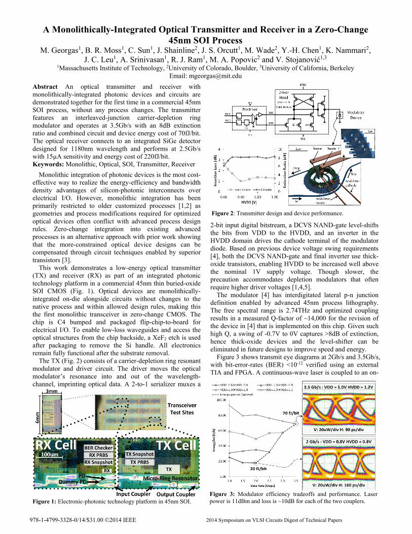
The TX (Fig. 2) consists of a carrier-depletion ring resonant modulator and driver circuit. The driver moves the optical modulator’s resonance into and out of the wavelength-channel, imprinting optical data. A 2-to-1 serializer muxes a
2-bit input digital bitstream, a DCVS NAND-gate level-shifts the bits from VDD to the HVDD, and an inverter in the HVDD domain drives the cathode terminal of the modulator diode. Based on previous device voltage swing requirements [4], both the DCVS NAND-gate and final inverter use thick-oxide transistors, enabling HVDD to be increased well above the nominal 1V supply voltage. Though slower, the precaution accommodates depletion modulators that often require higher driver voltages [1,4,5].
The modulator [4] has interdigitated lateral p-n junction definition enabled by advanced 45nm process lithography. The free spectral range is 2.74THz and optimized coupling results in a measured Q-factor of ~14,000 for the revision of the device in [4] that is implemented on this chip. Given such high Q, a swing of -0.7V to 0V captures >8dB of extinction, hence thick-oxide devices and the level-shifter can be eliminated in future designs to improve speed and energy.
Figure 3 shows transmit eye diagrams at 2Gb/s and 3.5Gb/s, with bit-error-rates (BER) <10-12 verified using an external TIA and FPGA. A continuous-wave laser is coupled to an on-
Figure 2: Transmitter design and device performance.
Figure 1: Electronic-photonic technology platform in 45nm SOI. Figure 3: Modulator efficiency tradeoffs and performance. Laser power is 11dBm and loss is ~10dB for each of the two couplers.
978-1-4799-3328-0/14/$31.00 ©2014 IEEE 2014 Symposium on VLSI Circuits Digest of Technical Papers
chip waveguide through a vertical grating. The modulator imprints data onto the wavelength-channel, and the modulated light propagates to a second grating and exits the chip. A layout error resulting in delay-imbalanced 0-to-1 and 1-to-0 paths through the thick-oxide DCVS NAND gate causes the distorted eye shape and ultimately limits the data-rate. Higher HVDD is required at higher data-rates solely for improving rise and fall times limited by slow thick-oxide driver devices. With appropriate supply scaling, driver energy-cost scales from 20fJ/bit at 2Gb/s to 70fJ/bit at 3.5Gb/s. The modulator’s reverse-bias operation and the driver’s digital implementation result in a flat energy-cost vs. data-rate, more than an order of magnitude better than the forward-bias injection modulator shown previously in the same process [3].
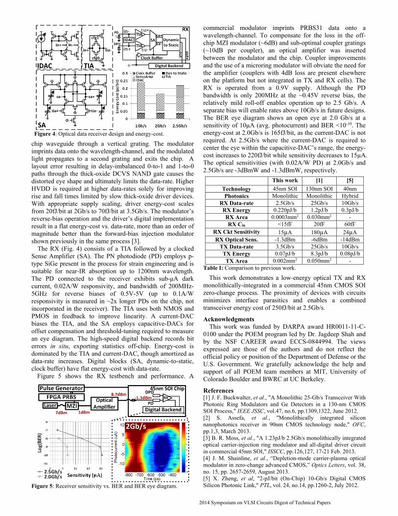
The RX (Fig. 4) consists of a TIA followed by a clocked Sense Amplifier (SA). The PN photodiode (PD) employs p-type SiGe present in the process for strain engineering and is suitable for near-IR absorption up to 1200nm wavelength. The PD connected to the receiver exhibits sub-μA dark current, 0.02A/W responsivity, and bandwidth of 200MHz-5GHz for reverse biases of 0.5V-5V (up to 0.1A/W responsivity is measured in ~2x longer PDs on the chip, not incorporated in the receiver). The TIA uses both NMOS and PMOS in feedback to improve linearity. A current-DAC biases the TIA, and the SA employs capacitive-DACs for offset compensation and threshold-tuning required to measure an eye diagram. The high-speed digital backend records bit errors in situ, exporting statistics off-chip. Energy-cost is dominated by the TIA and current-DAC, though amortized as data-rate increases. Digital blocks (SA, dynamic-to-static, clock buffer) have flat energy-cost with data-rate.
Figure 5 shows the RX testbench and performance. A
commercial modulator imprints PRBS31 data onto a wavelength-channel. To compensate for the loss in the off-chip MZI modulator (~6dB) and sub-optimal coupler gratings (~10dB per coupler), an optical amplifier was inserted between the modulator and the chip. Coupler improvements and the use of a microring modulator will obviate the need for the amplifier (couplers with 4dB loss are present elsewhere on the platform but not integrated in TX and RX cells). The RX is operated from a 0.9V supply. Although the PD bandwidth is only 200MHz at the ~0.45V reverse bias, the relatively mild roll-off enables operation up to 2.5 Gb/s. A separate bias will enable rates above 10Gb/s in future designs. The BER eye diagram shows an open eye at 2.0 Gb/s at a sensitivity of 10µA (avg. photocurrent) and BER <10-10. The energy-cost at 2.0Gb/s is 165fJ/bit, as the current-DAC is not required. At 2.5Gb/s where the current-DAC is required to center the eye within the capacitive-DAC’s range, the energy-cost increases to 220fJ/bit while sensitivity decreases to 15µA. The optical sensitivities (with 0.02A/W PD) at 2.0Gb/s and 2.5Gb/s are -3dBmW and -1.3dBmW, respectively.
This work [1] [5]
Technology 45nm SOI 130nm SOI 40nm Photonics Monolithic Monolithic Hybrid
RX Data-rate 2.5Gb/s 25Gb/s 10Gb/s RX Energy 0.220pJ/b 1.2pJ/b 0.3pJ/b RX Area 0.0003mm2 0.030mm2 - RX Cin <15fF 20fF 60fF
RX Ckt Sensitivity 15µA 180µA 24µA RX Optical Sens. -1.3dBm -6dBm -14dBm
TX Data-rate 3.5Gb/s 25Gb/s 10Gb/s TX Energy 0.07pJ/b 8.3pJ/b 0.08pJ/b TX Area 0.002mm2 0.050mm2 -
Table I: Comparison to previous work.
This work demonstrates a low-energy optical TX and RX monolithically-integrated in a commercial 45nm CMOS SOI zero-change process. The proximity of devices with circuits minimizes interface parasitics and enables a combined transceiver energy cost of 250fJ/bit at 2.5Gb/s.
Acknowledgments This work was funded by DARPA award HR0011-11-C-
0100 under the POEM program led by Dr. Jagdeep Shah and by the NSF CAREER award ECCS-0844994. The views expressed are those of the authors and do not reflect the official policy or position of the Department of Defense or the U.S. Government. We gratefully acknowledge the help and support of all POEM team members at MIT, University of Colorado Boulder and BWRC at UC Berkeley.
References [1] J. F. Buckwalter, et al., "A Monolithic 25-Gb/s Transceiver With Photonic Ring Modulators and Ge Detectors in a 130-nm CMOS SOI Process," IEEE JSSC, vol.47, no.6, pp.1309,1322, June 2012. [2] S. Assefa, et al., "Monolithically integrated silicon nanophotonics receiver in 90nm CMOS technology node," OFC, pp.1,3, March 2013. [3] B. R. Moss, et al., "A 1.23pJ/b 2.5Gb/s monolithically integrated optical carrier-injection ring modulator and all-digital driver circuit in commercial 45nm SOI," ISSCC, pp.126,127, 17-21 Feb. 2013. [4] J. M. Shainline, et al., “Depletion-mode carrier-plasma optical modulator in zero-change advanced CMOS,” Optics Letters, vol. 38, no. 15, pp. 2657-2659, August 2013. [5] X. Zheng, et al, "2-pJ/bit (On-Chip) 10-Gb/s Digital CMOS Silicon Photonic Link," PTL, vol. 24, no.14, pp.1260-2, July 2012.
Figure 4: Optical data receiver design and energy-cost.
Figure 5: Receiver sensitivity vs. BER and BER eye diagram.
2014 Symposium on VLSI Circuits Digest of Technical Papers