Embed Size (px)
Citation preview
A multifunctional molecular spintronic platformwith magnetoresistive and memristive responsesvia a self-assembled monolayer
Cite as: J. Appl. Phys. 125, 142905 (2019); doi: 10.1063/1.5057893
View Online Export Citation CrossMarkSubmitted: 16 September 2018 · Accepted: 4 November 2018 ·Published Online: 28 March 2019
Jhen-Yong Hong,1,2,a) Shih-Hang Chang,1 Kui-Hon Ou Yang,1 Piin-Chen Yeh,1 Hung-Wei Shiu,3 Chia-Hao Chen,3
Wen-Chung Chiang,4,b) and Minn-Tsong Lin1,5,b)
AFFILIATIONS
1Department of Physics, National Taiwan University, 10617 Taipei, Taiwan2Department of Physics, Tamkang University, 25137 New Taipei City, Taiwan3National Synchrotron Radiation Research Center, 30076 Hsinchu, Taiwan4Department of Optoelectric Physics, Chinese Culture University, 11114 Taipei, Taiwan5Institute of Atomic and Molecular Sciences, Academia Sinica, 10617 Taipei, Taiwan
a)This research was performed while Jhen-Yong Hong was at Department of Physics, National Taiwan University,
10617 Taipei, Taiwan.b)Authors to whom correspondence should be addressed: [email protected] and [email protected]
ABSTRACT
We report the spin-dependent transport and the I-V hysteretic characteristics in molecular-level organic spin valves containing a self-assem-bled-monolayer (SAM) barrier of 1,4 benzenedimethanethiol (BDMT). X-ray photoelectron spectroscopy confirms the establishment of anordered self-assembled monolayer of BDMT with the phosphonic groups coordinated onto the ferromagnet surface. The magnetoresistive(MR) and the I-V curves characterize the transport properties of the SAM-based organic spin valves, which exhibit both types of non-vola-tile memory switching, i.e., the magnetoresistive and the memristive switching. The results reveal the possibility of integrating organic SAMinto the future multifunctional molecular-level spintronic device applications.
Published under license by AIP Publishing. https://doi.org/10.1063/1.5057893
INTRODUCTION
The fast development of organic/inorganic hybrid hetero-junctions opens up new possibilities of integrating multi-functionalitiesinto modern electronic devices, which were previously not feasibleby the conventional metallic/inorganic hetero-junction structure.While simple organic/metallic junctions have been demonstrated tobe highly applicable to a variety of electronics,1–3 novel organic/ferro-magnetic (FM) hetero-structures, which combine the versatility oforganic materials and the spin-degree of freedom of ferromagnets,have just been realized in a number of spintronic applications,such as organic spin valve (OSV), spin-enhanced organic light-emitting diode (OLED), and photovoltaic device.4–7 However, thecreation of such hetero-junctions with well-defined organic/FMinterfaces, which are sensitively impacted by the growth conditionand the materials’ compatibility, is a great challenge.8–11 Upon the
contact of organic and FM materials, issues like the molecularordering and the interlayer diffusion and interaction not onlyaffect the transport properties of the junction but also entanglewith one another, complicating the investigation.9,12,13 Recently,the techniques of the Langmuir-Blodgett (LB) film and the self-assembled monolayer (SAM) with a large-area junction have beenproposed for solving the complicated active-layer problem andhave been adopted in several nano-scale devices.14–16 The incor-poration of SAM is technologically advantageous not only becauseof the potential for establishing a down-scaling, bottom-up build-ing block but also because of the flexibility of molecule choices,selective growth, and tailored functionality. Nevertheless, thestudies of embedding SAM into organic spintronic devices areonly preliminary, and a few examples can be seen in molecularOSV with nano-pore structures.17–19
Journal ofApplied Physics ARTICLE scitation.org/journal/jap
J. Appl. Phys. 125, 142905 (2019); doi: 10.1063/1.5057893 125, 142905-1
Published under license by AIP Publishing.
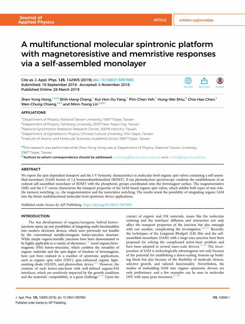
In this work, we report the spin-dependent transport properties ofa molecular-level OSV device containing a well-ordered organic-SAMlayer of 1,4 benzenedimethanethiol (BDMT) of thickness≈ 1 nm, asconfirmed by the X-ray photoelectron spectroscopy (XPS) analysis.In addition to the typical magnetoresistive (MR) effect, the devicealso exhibits non-volatile electrical memristive characteristics, leadingto the possibility of implanting multiple functions into a singledevice. The non-volatile electrical resistive-switching effect, or notedas the memristive effect, has received intensive attention in the pastfew years due to the potential for memory applications in modernelectronic devices.20,21 The effect is characterized by the non-volatilehysteresis of junction resistance (called the memristance) upon thecycling of the applied current or voltage. Depending on the type ofmaterials, memristance can be of different origins. For example, thehysteretic current-voltage characteristics demonstrated by thesemiconductor-based memristors are attributed to the interactionof electronic and ionic transports driven by the external voltage atthe oxide active layer.22,23 This non-volatile effect provides a play-ground for developing electronics with different and complemen-tary operations,24–26 since a multifunctional device (with electrical,magnetic, and/or optical inputs) on the same chip offers moreexternal control options and in the meantime simplifies its hierar-chical structure. The memristive effect has also been reported inorganic devices either in the form of thin films or containing aself-assembled monolayer.27,28 Nevertheless, reports of such multi-functional SAM device applications are still quite limited. Here, weinvestigate the mechanism of charge transport in a SAM-basedOSV system by fitting the I-V curves with the Simmons’ formula,and the results infer that charge trapping at the organic-SAM/FMinterface is mainly responsible for the hysteretic I-V behavior. Wehope that the work is beneficial to the development of future mul-tifunctional, molecular-level organic spintronic devices.
EXPERIMENT
The structure of the SAM-based organic spin valve is stackedin the sequence of NiFe (15 nm)/CoFe (10 nm)/BDMT (1 nm)/AlOx
(1 nm)/CoFe (35 nm) and patterned in a crossbar configuration,with the bottom NiFe/CoFe layer designed as the soft ferromagnetic(FM) electrode and the top CoFe as the hard FM electrode [seeFig. 1(a) for the schematic illustration]. The entire fabricationprocess was executed in a UHV sputtering chamber except the partof grafting the BDMT self-assembled monolayer onto the bottomFM electrode, which was accomplished by immersing the substrate(with the bottom electrode layer) into a freshly N2 bubblingdegassed 5 mM solution of n-Decane for 24 h. The sample wasthen rinsed with the same solution and dried under a stream ofnitrogen gas before transporting back into the UHV chamber forthe deposition of the capping AlOx and top electrode (TE) layers.The junction resistance and the MR effect, measured in theCurrent-Perpendicular-to-the-Plane (CPP) configuration with theapplied magnetic field parallel to the bottom electrode, were obtainedby the four-point-probe method. The electronic properties of theBDMT-SAM/FM interface were investigated on a separate set ofsamples made intentionally without the capping AlOx and the CoFelayers, but under the identical conditions as the regular OSV samples,using XPS at Beamline 09A1 of the National Synchrotron Radiation
Research Center (NSRRC) in Taiwan, with a 0.12 eV energy resolu-tion set by the pass energy of 5.85 eV of the Hemispherical SectorAnalyzer (HSA). The XPS spectra were analyzed by the convolutionof Lorentzian and Gaussian contributions, i.e., the so-called Voigtprofile, using the UNFIT simulation program.
RESULTS AND DISCUSSION
Figure 1(b) shows the C 1s and S 2p core-level XPS spectra ofthe BDMT self-assembled monolayer (SAM) grafted onto CoFe.Since XPS is a relatively surface-sensitive technique with a probingdepth typically less than 2 nm, the BDMT SAM used in the XPS
FIG. 1. (a) Structural schematic of the tri-layered molecular-level organic spin-valve (OSV) dusted with partially oxidized alumina at the top organic semicon-ductor (OSC)/FM interface. (b) The XPS S 2p and C 1s spectra of the BDMTself-assembled monolayer grafted onto the CoFe underlayer. The open circlesindicate the measured XPS data, whereas the orange curves are the best fitsobtained by superimposing the individual components.
Journal ofApplied Physics ARTICLE scitation.org/journal/jap
J. Appl. Phys. 125, 142905 (2019); doi: 10.1063/1.5057893 125, 142905-2
Published under license by AIP Publishing.
study is therefore suitable for distinguishing the interface-bondedand the free-standing end groups. The S 2p spectrum shown inFig. 1(b) has been normalized to the photon flux with the back-ground signal subtracted. The spectrum reveals a good signal/noise(s/n) ratio of the synchrotron generated x-ray source and is fittedwith the Voigt-doublet profiles. For each S 2p doublet, a 1.2 eVspin-orbit splitting and a 2:1 branching ratio between the 3/2 andthe 1/2 components are adopted, with the peaks within each doubletassumed to be of the same width. The main doublet at 163.3 (S2),with a full-width-half-maximum (FWHM) of 0.87 eV, is associatedwith the unbound sulfur, i.e., sulfur not directly engaged in a thiolatemolecule S-OH surface interaction, as, for example, the free thiol(SH) groups or the S-S bonds. The lower binding energy componentat 162.4 (S1), with a FWHM of 0.87 eV, is assigned to the thiolatesulfur bound to the CoFe substrate. Note that the absence of higherbinding energy components (above 166 eV)29,30 excludes the pres-ence of oxidized sulfur species in the present SAM. The XPS spectraof Fe and Co taken on a control sample of NiFe/CoFe/SAM-BDMT/AlOx (identical OSV without the top electrode) exhibit no evidentsigns of oxidation, indicating that the CoFe surface remains mostlyintact during the fabrication process.
Information on the establishment of a compact monolayer canbe obtained by examining the S2/S1 (unbound/bound S) intensityratio. In the present case, this ratio is 4.4, matching the value of 4that is expected from a single layer of molecules standing upright.31
This ratio is noticeably less than the values 5.4–6.3 as obtained inBDMT films prepared by room-temperature dipping in solvents for24 h.31 The result indicates that the preparation method adopted in
this study yields a single-layer film, with the molecules presumably ina vertical configuration. The inset of Fig. 1(b) shows the presence of asingle C 1 s structure with its maximum intensity located at 284.8 eV.The main photoemission contribution at 284.8 eV can be attributedto the aromatic carbon atoms and the carbon atoms in the methyleneunits, whereas the higher binding energy tail is likely related to theshake-up process that produces aromatic rings in the organic film.
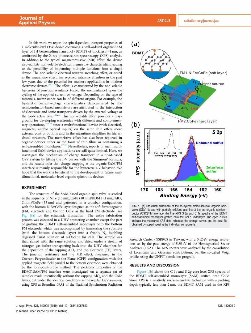
For magneto-transport characterization, Fig. 2(a) shows thecycling of junction resistance with applied magnetic field, measuredat a low-resistance state (LRS, see below) with a constant current of10 μA, for a SAM-based OSV. The resistance curves display thetypical pseudo spin-valve type characteristics at room temperature(RT) with a magneto-resistive (MR) ratio of 0.25%, where the MRratio is defined as
ΔRRP
¼ RAP � RP
RP, (1)
with RP and RAP depicting the resistances when the magnetizationsof the FM electrodes are in the parallel and antiparallel configura-tions, respectively. The MR ratio increases substantially at cryogenictemperatures, i.e., 1.9% at 100 K and 2.4% at 20 K, as seen inFig. 2(a). The junction resistance itself increases by a factor of 2.3when the temperature is decreased from RT to 20 K [see Fig. 2(b)],showing an agreement with the organic semiconductor behav-ior.13,32 To ensure that the MR effect is not resulted from the tun-neling through the thin alumina layer, a control sample is made
FIG. 2. (a) Magnetoresistive curves at20 K, 100 K, and 300 K and (b) thetemperature dependence of the MRratio (referenced to the right axis) andthe junction resistance (normalized tothe room-temperature resistance, refer-enced to the left axis) of a SAM-basedorganic spin valve. (c) The temperaturedependence of the junction resistanceof a control sample made without theSAM layer (see text). All data shownare measured at a constant currentmode (10 μA) under LRS condition(see text).
Journal ofApplied Physics ARTICLE scitation.org/journal/jap
J. Appl. Phys. 125, 142905 (2019); doi: 10.1063/1.5057893 125, 142905-3
Published under license by AIP Publishing.
with an identical structure but without the organic SAM layer. Ourprevious XPS study on organic spin valves indicates that when theorganic molecules are in direct contact with the ferromagnetic Counderlayer, a strong chemical interaction between Co and themolecular functional groups occurs, leading to the formation of aCoO complex that would suppress the spin injection from Co intothe organic layer.9 The introduction of a thin AlOx layer at theFM/organic interface blocked the chemical interaction and effec-tively restored the spin injection. Besides, in OSVs, the junctionresistance and MR ratio depend strongly on temperature, whereasin oxide-based tunnel junctions, the dependence is less substantial.In the present study, the control sample shows a zero MR ratioand a junction resistance≈ 20Ω at RT. Moreover, Fig. 2(c) revealsthat the control sample’s resistance follows the typical metallicbehavior. These results indicate that the MR effect exhibited bythe SAM-based OSV comes from the spin-dependent transportthrough the organic SAM layer rather than from the thin aluminalayer (note that the OSV with SAM-BDMT shows no-broken junc-tion resistance). In particular, the temperature dependence of theresistance suggests that the transport within the SAM layer is nota simple tunneling process, but rather a hopping process via local-ized states.
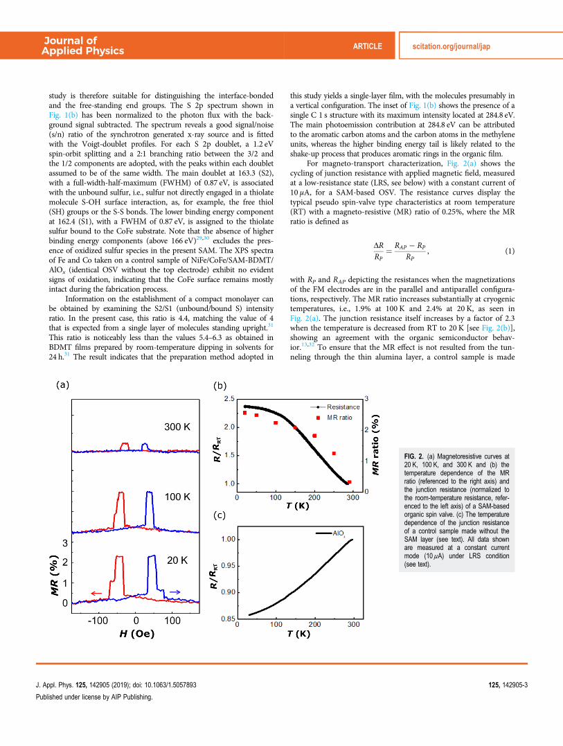
Figure 3(a) shows the room-temperature, zero-field I-V curvesof the SAM-based organic spin valve with the top electrode beingnegative (i.e., current flows from bottom to top). The pinched hys-teresis loop is the fingerprint of a memristive device. The deviceswitches between the low-resistance state (LRS) and the highresistance state (HRS) upon current sweep; once the resistanceis switched, the device remains in the same state until the oppositemaximum current is reached. Compared to the I-V curvesobtained from scanning tunneling microscopy (STM) measure-ments that show no hysteresis,33 the cause of intrinsic switching ofthe molecules can be eliminated. The pinched I-V hysteresis char-acteristic is the key to the application of resistive switchingmemory. Figure 3(b) shows the read-write-read-erase cycle whenthe SAM-based organic device is exposed to pulsed current wherethe write/read/erase current is set at 4 mA/1 mA/−4 mA and thepulse interval at 1 ms, respectively. During the cycling, the resis-tance is switched to HRS upon applying the write current, whereas
a higher resistance state is obtained by applying the read current.The erase pulse brings the device back to LRS. Such characteristicscan represent the basic logic elements, i.e., 0 and 1, of a memorydevice.
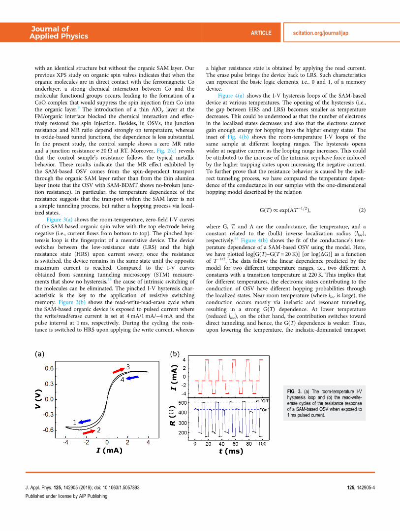
Figure 4(a) shows the I-V hysteresis loops of the SAM-baseddevice at various temperatures. The opening of the hysteresis (i.e.,the gap between HRS and LRS) becomes smaller as temperaturedecreases. This could be understood as that the number of electronsin the localized states decreases and also that the electrons cannotgain enough energy for hopping into the higher energy states. Theinset of Fig. 4(b) shows the room-temperature I-V loops of thesame sample at different looping ranges. The hysteresis openswider at negative current as the looping range increases. This couldbe attributed to the increase of the intrinsic repulsive force inducedby the higher trapping states upon increasing the negative current.To further prove that the resistance behavior is caused by the indi-rect tunneling process, we have compared the temperature depen-dence of the conductance in our samples with the one-dimensionalhopping model described by the relation
G(T)/ exp(AT�1=2), (2)
where G, T, and A are the conductance, the temperature, and aconstant related to the (bulk) inverse localization radius (lloc),respectively.34 Figure 4(b) shows the fit of the conductance’s tem-perature dependence of a SAM-based OSV using the model. Here,we have plotted log[G(T)–G(T = 20 K)] [or log(ΔG)] as a functionof T−1/2. The data follow the linear dependence predicted by themodel for two different temperature ranges, i.e., two different Aconstants with a transition temperature at 220 K. This implies thatfor different temperatures, the electronic states contributing to theconduction of OSV have different hopping probabilities throughthe localized states. Near room temperature (where lloc is large), theconduction occurs mostly via inelastic and resonant tunneling,resulting in a strong G(T) dependence. At lower temperature(reduced lloc), on the other hand, the contribution switches towarddirect tunneling, and hence, the G(T) dependence is weaker. Thus,upon lowering the temperature, the inelastic-dominated transport
FIG. 3. (a) The room-temperature I-Vhysteresis loop and (b) the read-write-erase cycles of the resistance responseof a SAM-based OSV when exposed to1 ms pulsed current.
Journal ofApplied Physics ARTICLE scitation.org/journal/jap
J. Appl. Phys. 125, 142905 (2019); doi: 10.1063/1.5057893 125, 142905-4
Published under license by AIP Publishing.
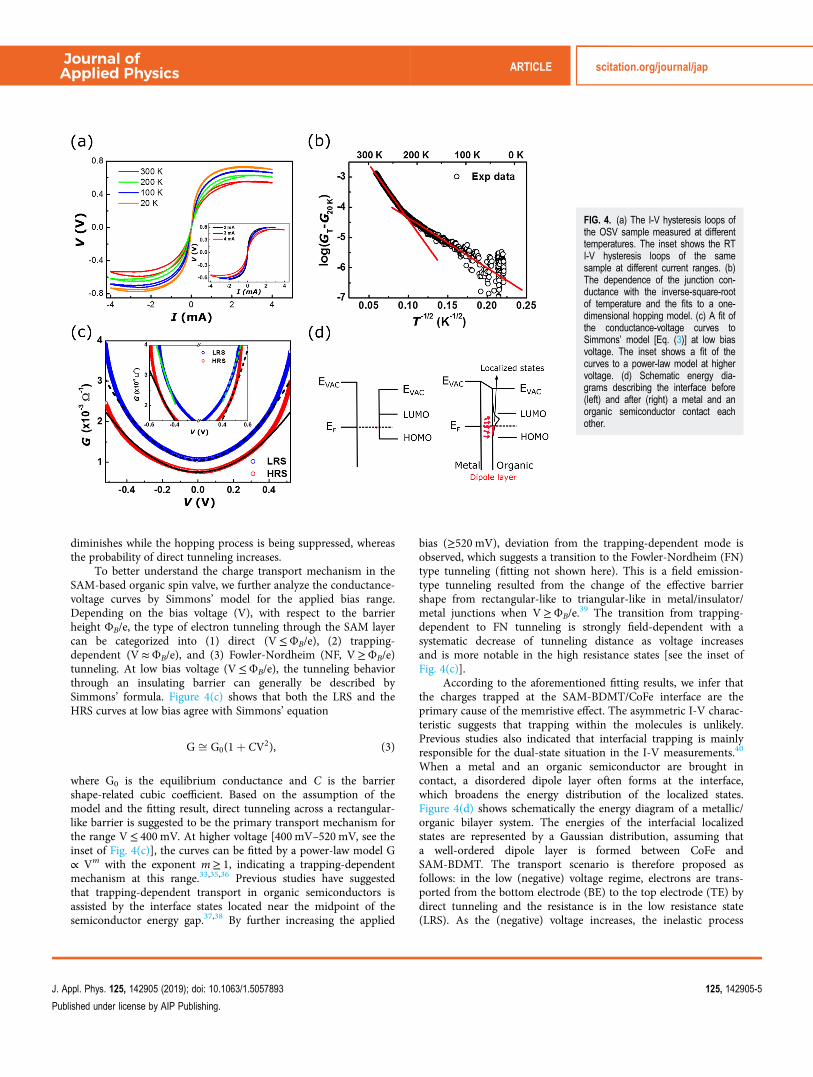
diminishes while the hopping process is being suppressed, whereasthe probability of direct tunneling increases.
To better understand the charge transport mechanism in theSAM-based organic spin valve, we further analyze the conductance-voltage curves by Simmons’ model for the applied bias range.Depending on the bias voltage (V), with respect to the barrierheight ΦB/e, the type of electron tunneling through the SAM layercan be categorized into (1) direct (V≤ΦB/e), (2) trapping-dependent (V≈ΦB/e), and (3) Fowler-Nordheim (NF, V≥ΦB/e)tunneling. At low bias voltage (V≤ΦB/e), the tunneling behaviorthrough an insulating barrier can generally be described bySimmons’ formula. Figure 4(c) shows that both the LRS and theHRS curves at low bias agree with Simmons’ equation
G ffi G0(1þ CV2), (3)
where G0 is the equilibrium conductance and C is the barriershape-related cubic coefficient. Based on the assumption of themodel and the fitting result, direct tunneling across a rectangular-like barrier is suggested to be the primary transport mechanism forthe range V≤ 400 mV. At higher voltage [400 mV–520 mV, see theinset of Fig. 4(c)], the curves can be fitted by a power-law model G∝ Vm with the exponent m≥ 1, indicating a trapping-dependentmechanism at this range.33,35,36 Previous studies have suggestedthat trapping-dependent transport in organic semiconductors isassisted by the interface states located near the midpoint of thesemiconductor energy gap.37,38 By further increasing the applied
bias (≥520 mV), deviation from the trapping-dependent mode isobserved, which suggests a transition to the Fowler-Nordheim (FN)type tunneling (fitting not shown here). This is a field emission-type tunneling resulted from the change of the effective barriershape from rectangular-like to triangular-like in metal/insulator/metal junctions when V≥ΦB/e.
39 The transition from trapping-dependent to FN tunneling is strongly field-dependent with asystematic decrease of tunneling distance as voltage increasesand is more notable in the high resistance states [see the inset ofFig. 4(c)].
According to the aforementioned fitting results, we infer thatthe charges trapped at the SAM-BDMT/CoFe interface are theprimary cause of the memristive effect. The asymmetric I-V charac-teristic suggests that trapping within the molecules is unlikely.Previous studies also indicated that interfacial trapping is mainlyresponsible for the dual-state situation in the I-V measurements.40
When a metal and an organic semiconductor are brought incontact, a disordered dipole layer often forms at the interface,which broadens the energy distribution of the localized states.Figure 4(d) shows schematically the energy diagram of a metallic/organic bilayer system. The energies of the interfacial localizedstates are represented by a Gaussian distribution, assuming thata well-ordered dipole layer is formed between CoFe andSAM-BDMT. The transport scenario is therefore proposed asfollows: in the low (negative) voltage regime, electrons are trans-ported from the bottom electrode (BE) to the top electrode (TE) bydirect tunneling and the resistance is in the low resistance state(LRS). As the (negative) voltage increases, the inelastic process
FIG. 4. (a) The I-V hysteresis loops ofthe OSV sample measured at differenttemperatures. The inset shows the RTI-V hysteresis loops of the samesample at different current ranges. (b)The dependence of the junction con-ductance with the inverse-square-rootof temperature and the fits to a one-dimensional hopping model. (c) A fit ofthe conductance-voltage curves toSimmons’ model [Eq. (3)] at low biasvoltage. The inset shows a fit of thecurves to a power-law model at highervoltage. (d) Schematic energy dia-grams describing the interface before(left) and after (right) a metal and anorganic semiconductor contact eachother.
Journal ofApplied Physics ARTICLE scitation.org/journal/jap
J. Appl. Phys. 125, 142905 (2019); doi: 10.1063/1.5057893 125, 142905-5
Published under license by AIP Publishing.
rises, and the number of electrons trapped in the interfacial local-ized states soars, creating a repulsive force. When the (negative)voltage is inversed, the resistance switches to the high-resistancestate (HRS) since the Coulomb repulsion of the trapped electrons isnow stronger. Upon the (negative) voltage decrease, more electronshop into the BE than those from the TE into the localized states.The hopping process into the BE is easier due to the energy distri-bution of the states, and therefore, the resistance switches back tothe LRS until the (positive) voltage reaches the switching threshold.Note that the MR effect is obtained only at LRS and there is noMR at HRS. This could be due to the interfacial dipole/localizedstates at HRS, which cause spin scattering/flipping, while the spin-polarized electrons transport through the SAM-BDMT layer.
CONCLUSION
In conclusion, we have demonstrated a reliable approach tocontact a self-assembled molecular monolayer onto a ferromagneticunderlayer with the contact area larger than 150 × 150 μm2, whichforms the basis of a hybrid ferromagnetic/SAM/ferromagneticorganic spin valve. The OSV device exhibits both magnetoresis-tance and non-volatile resistive memory switching, with the ferro-magnetic layers acting as a spin-polarized injector and a detector.The electronic transport of the system goes through sequentialtransitions from direct tunneling, trapping-dependent hopping, toFowler-Nordheim tunneling at different stages of applied bias.The unique properties of OSV demonstrated in this study revealthe possibility of integrating SAM into future multi-functionalmolecular-level organic spintronic devices.
ACKNOWLEDGMENTS
This work is supported by the Ministry of Science andTechnology of Taiwan (Grant No. MOST-104-2811-M-002-201).
REFERENCES1C. Wang, H. Dong, W. Hu, Y. Liu, and D. Zhu, Chem. Rev. 112, 2208 (2011).2M. Berggren, D. Nilsson, and N. D. Robinson, Nat. Mater. 6, 3 (2007).3T. Sekitani and T. Someya, Adv. Mater. 22, 2228 (2010).4Z. Xiong, D. Wu, Z. V. Vardeny, and J. Shi, Nature 427, 821 (2004).5T. D. Nguyen, E. Ehrenfreund, and Z. V. Vardeny, Science 337, 204 (2012).6D. Sun, E. Ehrenfreund, and Z. V. Vardeny, Chem. Comm. 50, 1781 (2014).7J. Devkota, R. Geng, R. C. Subedi, and T. D. Nguyen, Adv. Funct. Mater. 26,3881 (2016).8S. Jiang, D. Shu, L. Lin, Y. Shi, J. Shi, H. Ding, J. Du, M. Wang, and D. Wu,New J. Phys. 16, 013028 (2014).9J.-Y. Hong et al., Appl. Phys. Lett. 104, 083301 (2014).
10M. Galbiati, S. Tatay, S. Delprat, H. Le Khanh, B. Servet, C. Deranlot, S. Collin,P. Seneor, R. Mattana, and F. Petroff, Appl. Phys. Lett. 106, 082408 (2015).11R. Geng, A. Roy, W. Zhao, R. C. Subedi, X. Li, J. Locklin, and T. D. Nguyen,Adv. Funct. Mater. 26, 3999 (2016).12K. Raman, S. Watson, J. A. A. Shim, J. Borchers, J. Chang, and J. Moodera,Phys. Rev. B 80, 195212 (2009).13K.-S. Li, Y.-M. Chang, S. Agilan, J.-Y. Hong, J.-C. Tai, W.-C. Chiang,K. Fukutani, P. Dowben, and M.-T. Lin, Phys. Rev. B 83, 172404 (2011).14M. Halik and A. Hirsch, Adv. Mater. 23, 2689 (2011).15T. Schmaltz, A. Y. Amin, A. Khassanov, T. Meyer-Friedrichsen,H.-G. Steinrück, A. Magerl, J. J. Segura, K. Voitchovsky, F. Stellacci, andM. Halik, Adv. Mater. 25, 4511 (2013).16Y. Ando, J. Murai, T. Miyashita, and T. Miyazaki, Thin Solid Films 331, 158(1998).17J. Petta, S. Slater, and D. Ralph, Phys. Rev. Lett. 93, 136601 (2004).18M. Galbiati, C. Barraud, S. Tatay, K. Bouzehouane, C. Deranlot, E. Jacquet,A. Fert, P. Seneor, R. Mattana, and F. Petroff, Adv. Mater. 24, 6429 (2012).19S. Tatay et al., ACS Nano 6, 8753 (2012).20T. Prodromakis, C. Toumazou, and L. Chua, Nat. Mater. 11, 478 (2012).21D. B. Strukov, G. S. Snider, D. R. Stewart, and R. S. Williams, Nature 453, 80(2008).22Y. C. Bae, A. R. Lee, J. B. Lee, J. H. Koo, K. C. Kwon, J. G. Park, H. S. Im, andJ. P. Hong, Adv. Func. Mater. 22, 709 (2012).23A. Mazady and M. Anwar, IEEE Trans. Electron Devices 61, 1054 (2014).24L. E. Hueso, I. Bergenti, A. Riminucci, Y. Zhan, and V. Dediu, Adv. Mater. 19,2639 (2007).25A. Chanthbouala et al., Nature Mater. 11, 860 (2012).26T. Mosciatti, S. Haar, F. Liscio, A. Ciesielski, E. Orgiu, and P. Samori, ACSNano 9, 2357 (2015).27J. Chen, M. Reed, A. Rawlett, and J. Tour, Science 286, 1550 (1999).28M. Prezioso, A. Riminucci, I. Bergenti, P. Graziosi, D. Brunel, andV. A. Dediu, Adv. Mater. 23, 1371 (2011).29J. M. Tour, L. Jones, D. L. Pearson, J. J. Lamba, T. P. Burgin,G. M. Whitesides, D. L. Allara, A. N. Parikh, and S. Atre, J. Amer. Chem. Soc.117, 9529 (1995).30D. G. Castner, K. Hinds, and D. W. Grainger, Langmuir 12, 5083 (1996).31L. Pasquali, F. Terzi, C. Zanardi, L. Pigani, R. Seeber, G. Paolicelli, S. Suturin,N. Mahne, and S. Nannarone, Surf. Sci. 601, 1419 (2007).32T. Santos, J. Lee, P. Migdal, I. Lekshmi, B. Satpati, and J. Moodera, Phys. Rev.Lett. 98, 016601 (2007).33X. Xiao, B. Xu, and N. J. Tao, Nano Lett. 4, 267 (2004).34H. Bottger and V. V. Bryksin, Hopping Conduction in Solids (Akademie-Verlag, Berlin, 1985).35P. Mark and W. Helfrich, J. Appl. Phys. 33, 205 (1962).36D. Braun, J. Polym. Sci. B 41, 2622 (2003).37W. L. Kalb, S. Haas, C. Krellner, T. Mathis, and B. Batlogg, Phys. Rev. B 81,155315 (2010).38Z. G. Yu, Nat. Commun. 5, 4842 (2014).39I. D. Parker, J. Appl. Phys. 75, 1656 (1994).40B. Cho, S. Song, Y. Ji, T.-W. Kim, and T. Lee, Adv. Func. Mater. 21, 2806(2011).
Journal ofApplied Physics ARTICLE scitation.org/journal/jap
J. Appl. Phys. 125, 142905 (2019); doi: 10.1063/1.5057893 125, 142905-6
Published under license by AIP Publishing.