Embed Size (px)
Citation preview
© 2015 WILEY-VCH Verlag GmbH & Co. KGaA, Weinheim 1wileyonlinelibrary.com
FULL P
APER
A New Perspective on Plasmonics: Confi nement and Propagation Length of Surface Plasmons for Different Materials and Geometries
Babak Dastmalchi , Philippe Tassin , * Thomas Koschny , and Costas M. Soukoulis
B. Dastmalchi, T. Koschny, C. M. Soukoulis Ames Laboratory, U.S. DOE and Department of Physics and Astronomy Iowa State University Ames , IA 50011 , USA B. Dastmalchi, C. M. Soukoulis Institute of Electronic Structure and Lasers (IESL) FORTH 71110 Heraklion , Crete , Greece P. Tassin Department of Applied Physics Chalmers University SE-412 96 Göteborg , Sweden E-mail: [email protected]
DOI: 10.1002/adom.201500446
the forefront of optical sciences during the last decades. [ 7–15 ] Indeed, the ability to squeeze optical energy into subwavelength volumes [ 16 ] makes surface-plasmon modes attractive candidates for use in applications like biosensing, [ 17,18 ] nonlinear optics, [ 19,20 ] and solar energy, [ 21 ] where the extreme localization of electromagnetic fi elds can improve effi ciency, and in optical inter-connects and chips, [ 22–25 ] where the strong confi nement results in miniaturization and dense packing of electrical as well as optical elements with small footprint.
Nevertheless, the development of appli-cations based on plasmonic materials is hindered by dissipative loss. Because of conversion of optical energy to heat, [ 26 ] surface plasmons’ decay while propagating along the surface. The propagation length usually depends not only on the material properties of the supporting medium, but
also on its geometry, the frequency of operation, and the fi eld symmetry of the plasmon mode. However, adjusting these degrees of freedom as, for example, in long-range surface-plasmon modes [ 27 ] or using V-grooves, [ 28 ] normally results in a tradeoff between propagation length and level of confi nement. Therefore, researchers have recently started exploring new low-loss plasmonic materials, [ 29–34 ] including doped semiconduc-tors, metal alloys, and graphene. [ 35–39 ] The aim of this paper is to develop a coherent method to compare plasmonic materials carefully, taking the tradeoff between the propagation length and the degree of confi nement into consideration, and to provide a comprehensive overview of the performance of current bleeding-edge plasmonic materials using this universal framework.
2. Results
Our method is based on a two-dimensional relation of the two fundamental and competing aspects of all surface-plasmon waves: propagation length and degree of confi nement. Let us, therefore, fi rst defi ne how we will measure these two param-eters. Various defi nitions for the degree of confi nement in a plasmonic waveguide are encountered in the literature, either based on the spatial extent of the energy [ 40,41 ] or on the dis-tance over which the fi eld decays from its local maximum in a guiding geometry. [ 42 ] While they differ in how they treat the near-fi eld structure, they have in common that the confi nement
Surface-plasmon polaritons are electromagnetic waves propagating on the surface of a metal. Thanks to subwavelength confi nement, they can concen-trate optical energy on the micrometer or even nanometer scale, enabling new applications in bio-sensing, optical interconnects, and nonlinear optics, where small footprint and strong fi eld concentration are essential. The major obstacle in developing plasmonic applications is dissipative loss, which limits the propagation length of surface plasmons and broadens the bandwidth of surface-plasmon resonances. Here, a new analysis of plasmonic materials and geometries is presented which fully considers the tradeoff between prop-agation length and degree of confi nement. It is based on a two-dimensional analysis of two independent fi gures of merit and the analysis is applied to relevant plasmonic materials, e.g., noble metals, aluminum, silicon carbide, doped semiconductors, graphene, etc. The analysis provides guidance on how to improve the performance of any particular plasmonic application and substantially eases the selection of the plasmonic material.
1. Introduction
The propagation of electromagnetic waves at the surface of conducting media was studied as early as the beginning of the 20th century by Zeneck [ 1 ] and Sommerfeld [ 2 ] in the framework of the interaction of radio waves with the Earth. However, it was the work of Otto, [ 3,4 ] Economou, [ 5 ] and Kretschmann [ 6 ] that started the modern plasmonics fi eld by providing a detailed theoretical description and experimental methods to excite surface-plasmon polaritons (SPPs) on fi lms of noble metals. Because of advances in nanofabrication, characterization, and computational electromagnetism, plasmonics has moved to
Adv. Optical Mater. 2015, DOI: 10.1002/adom.201500446
www.MaterialsViews.comwww.advopticalmat.de
2 wileyonlinelibrary.com © 2015 WILEY-VCH Verlag GmbH & Co. KGaA, Weinheim
FULL
PAPER
FULL
PAPER
FULL
PAPER
www.MaterialsViews.comwww.advopticalmat.de
is predominantly determined by the exponential decay of the fi elds outside the plasmonic waveguide. The most intuitive defi -nition for a fi gure of merit (FOM) for the degree of confi nement is, then, the inverse of the distance over which the fi elds drop to 1/ e of their maximum amplitude when moving away from the supporting interface, normalized by the free-space wavelength λ 0 . If k⊥ is the modal wave number in the transverse direction, then the fi gure of merit is given by
1
Im, FOMconf
0
kδ λ
δ[ ]= =⊥
(1)
This fi gure-of-merit measures the confi nement of the sur-face wave with respect to the corresponding vacuum wave-length. There is more conformity in the literature about how to measure the propagation distance of a surface plasmon polar-iton L prop . It is usually defi ned as the distance over which the mode can propagate along the supporting interface until the fi eld amplitudes drop to 1/ e of their initial magnitude, now nor-malized by the surface-plasmon polariton wavelength λ spp
1
Im, FOM
Re
2 Improp prop
p
spp�
�
�
Lk
L k
kλ π[ ][ ]
[ ]= = = (2)
This fi gure of merit can effectively be thought of as how many wavelengths a surface-plasmon polariton mode can travel until its fi eld amplitude has died out. Evidently, both fi gures of
merit depend on the dispersion relation of the plasmon mode and, hence, they are infl uenced by material loss, the specifi c geometry of the waveguide, and the fi eld symmetry of the plasmon mode. It is desirable to have both FOMs as large as possible for general plasmonic applications. Unfortunately, this can usually not be achieved simultaneously.
2.1. Drude Materials
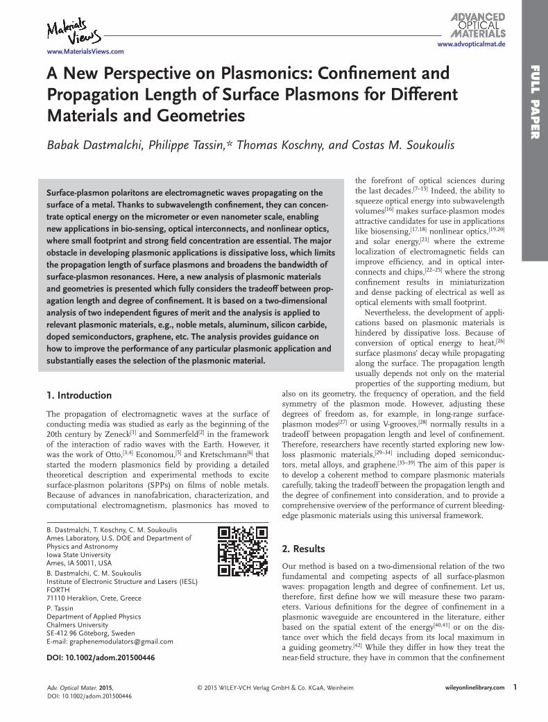
Surface plasmon polaritons are essentially transverse magnetic bound modes propagating at the interface of materials with permittivities of opposite sign (real part)—see Figure 1 a for a schematic of the fi elds and the currents. The majority of mate-rials with a negative permittivity—including the popular noble metals, transparent conducting oxides, and doped semiconduc-tors—can be fairly accurately modeled by a simple free-electron model, known as the Drude model, valid in frequency bands below the interband transition frequencies. Therefore, it will be insightful to fi rst understand the general plasmonic behavior of a material with Drude response
1i
p2
ε ωω
ω ω( )
( )= −
+ Γ (3)
where ω p 2 = nq 2 /( ε 0 m * ) and Γ are the plasma and collision frequencies, n is the density of the free charge carriers in the
Adv. Optical Mater. 2015, DOI: 10.1002/adom.201500446
Figure 1. Schematic geometries and fi eld/current distributions. a) Single interface. b) Conductive sheet. c) Insulator–metal–insulator. d) Metal–insu-lator–metal. For IMI and MIM structures, only the three modes with the lowest loss are plotted and the corresponding dispersion diagrams are shown at the right side. For the MIM case, the dielectric thickness is chosen small enough so that the guided modes do not appear in the plotted range. The total Poynting vector is positive for all cases.
3wileyonlinelibrary.com© 2015 WILEY-VCH Verlag GmbH & Co. KGaA, Weinheim
FULL P
APER
FULL P
APER
FULL P
APER
www.MaterialsViews.comwww.advopticalmat.de
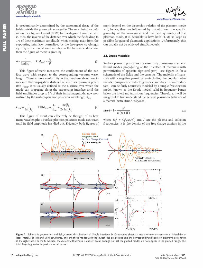
material, q and m * are the electrical charge and effective mass of the carriers, respectively, and ε 0 is the vacuum permittivity. Figure 2 a shows a logarithmic plot of the frequency-dependent permittivity of a Drude material and the dispersion relation of the surface-plasmon polaritons on its surface. We can recog-nize four distinct generic regions: region I below the collision frequency, where the metal is primarily a dissipative con-ductor; region II below the plasma frequency, where the metal is dominated by polarization current and behaves primarily as a lossy negative dielectric; region III around the plasma fre-quency; and region IV above the plasma frequency, where the metal is a lossy positive dielectric with superluminal phase velocity. In Figure 2 b, we show the two-dimensional FOM graph with the propagation fi gure of merit on the horizontal axis and the confi nement fi gure of merit on the vertical axis. Note that the low-frequency and high-frequency regions can be approximated by simple power laws, shown by thin lines in Figure 2 b, from which the tradeoff between confi nement and propagation length is evident. At the lowest frequencies, surface-plasmon waves have a very high propagation fi gure of merit, but since they are closely following the light line, they are only weakly confi ned to the interface—these solutions are commonly known as Zenneck–Sommerfeld waves. [ 1,2 ] The most interesting region for plasmonics is undoubtedly region IIIa, i.e., frequencies close to but still below ω spp = ω p / 2. Here the plasmonic modes exhibit the strongest subwavelength nature, and the best values for the fi gures of merit are found in this region. As the frequency approaches ω spp , the surface modes become very lossy, reducing the propagation distance to fractions of an SPP wavelength, especially for the part with negative slope (shown by the dashed line in the FOM graph of Figure 2 b). Once the dispersion curve crosses the light line, modes become leaky, and energy is radiated away from the surface. Finally, in the high-frequency limit, the propagation distance recovers; nevertheless, due to the leaky nature, solu-tions are no longer confi ned to the interface. The plasmons in region IIIa always offer the best confi nement–propagation tradeoff.
For a Drude material, there is essentially only one param-eter changing the shape of the two-dimensional FOM graph: the ratio of the collision frequency over the plasma frequency. Figure 2 c demonstrates the impact of variations of this ratio on the FOM graph. By lowering the collision frequency (essentially reducing the average momentum lost in collisions), the area enclosed by the FOM line expands to achieve a better tradeoff between the confi nement and propagation distance. It will, therefore, be desirable to choose materials with an as small as possible Γ / ω p ratio. Choosing a material with a different plasma frequency, while keeping Γ / ω p constant, allows shifting the frequency of operation.
The plasma frequency being proportional to the square root of the carrier density is also of importance for tunability. Bulk metals do not easily permit changes in the carrier concentra-tion. However, for some other classes of materials, such as nonstoichiometric compounds, [ 43 ] photon-induced conduc-tors, [ 44 ] and graphene, the carrier concentration can readily be changed by several orders of magnitude with electrical, [ 45,46 ] optical, or other methods of doping in order to functionalize the plasmonic properties. Increasing the carrier concentration
Adv. Optical Mater. 2015, DOI: 10.1002/adom.201500446
Figure 2. Dispersion relations and fi gures of merit. a) From left to right: real (black) and imaginary (red) parts of the permittivity, the parallel com-ponent of the wave vector, and the normal component of the wave vector. The green lines in the dispersion diagrams mark the vacuum light line. b) The behavior of the two FOMs for a conductor with Drude response. c) The dependence of the FOMs on the ratio of the collision frequency Γ to the plasma frequency ω p . d) Comparison of FOM relations for a pure Drude, and a Drude–Lorentz dielectric function. The Drude part for both curves is similar. The Lorentz term is centered at ω 0 = 0.6 ω p with a width of Γ = 1 × 10 −2 ω p and an oscillator strength of ω L = 0.7 ω p , and causes the additional loop in the graph.
4 wileyonlinelibrary.com © 2015 WILEY-VCH Verlag GmbH & Co. KGaA, Weinheim
FULL
PAPER
FULL
PAPER
FULL
PAPER
www.MaterialsViews.comwww.advopticalmat.de
will generally have two effects: (1) it will expand the FOM graph to better fi gures of merit in region IIIa, and (2) the frequency band of operation will be blueshifted.
At visible frequencies, interband transitions play an impor-tant role in most conductors, and a simple Drude model can no longer represent their optical response. The effect of interband transitions can be modeled by adding multiple resonators rep-resented by Lorentz terms. [ 47 ] In Figure 2 d, we show the FOM graph for a conductor with a single interband transition fre-quency. The FOM graph makes a loop with detrimental effect on the fi gures of merit. It is generally better to stay clear of interband transitions in plasmonic materials.
2.2. Summary of Real Materials
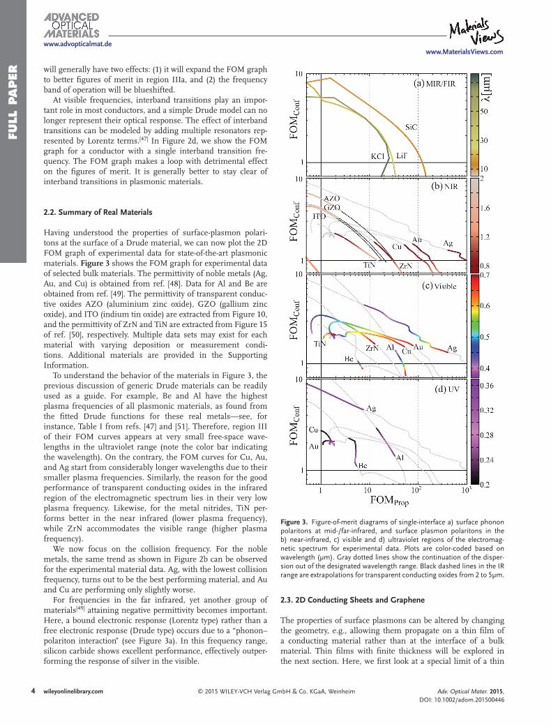
Having understood the properties of surface-plasmon polari-tons at the surface of a Drude material, we can now plot the 2D FOM graph of experimental data for state-of-the-art plasmonic materials. Figure 3 shows the FOM graph for experimental data of selected bulk materials. The permittivity of noble metals (Ag, Au, and Cu) is obtained from ref. [ 48 ] . Data for Al and Be are obtained from ref. [ 49 ] . The permittivity of transparent conduc-tive oxides AZO (aluminium zinc oxide), GZO (gallium zinc oxide), and ITO (indium tin oxide) are extracted from Figure 10, and the permittivity of ZrN and TiN are extracted from Figure 15 of ref. [ 50 ] , respectively. Multiple data sets may exist for each material with varying deposition or measurement condi-tions. Additional materials are provided in the Supporting Information.
To understand the behavior of the materials in Figure 3 , the previous discussion of generic Drude materials can be readily used as a guide. For example, Be and Al have the highest plasma frequencies of all plasmonic materials, as found from the fi tted Drude functions for these real metals—see, for instance, Table I from refs. [ 47 ] and [ 51 ] . Therefore, region III of their FOM curves appears at very small free-space wave-lengths in the ultraviolet range (note the color bar indicating the wavelength). On the contrary, the FOM curves for Cu, Au, and Ag start from considerably longer wavelengths due to their smaller plasma frequencies. Similarly, the reason for the good performance of transparent conducting oxides in the infrared region of the electromagnetic spectrum lies in their very low plasma frequency. Likewise, for the metal nitrides, TiN per-forms better in the near infrared (lower plasma frequency), while ZrN accommodates the visible range (higher plasma frequency).
We now focus on the collision frequency. For the noble metals, the same trend as shown in Figure 2 b can be observed for the experimental material data. Ag, with the lowest collision frequency, turns out to be the best performing material, and Au and Cu are performing only slightly worse.
For frequencies in the far infrared, yet another group of materials [ 49 ] attaining negative permittivity becomes important. Here, a bound electronic response (Lorentz type) rather than a free electronic response (Drude type) occurs due to a “phonon–polariton interaction” (see Figure 3 a). In this frequency range, silicon carbide shows excellent performance, effectively outper-forming the response of silver in the visible.
2.3. 2D Conducting Sheets and Graphene
The properties of surface plasmons can be altered by changing the geometry, e.g., allowing them propagate on a thin fi lm of a conducting material rather than at the interface of a bulk material. Thin fi lms with fi nite thickness will be explored in the next section. Here, we fi rst look at a special limit of a thin
Adv. Optical Mater. 2015, DOI: 10.1002/adom.201500446
Figure 3. Figure-of-merit diagrams of single-interface a) surface phonon polaritons at mid-/far-infrared, and surface plasmon polaritons in the b) near-infrared, c) visible and d) ultraviolet regions of the electromag-netic spectrum for experimental data. Plots are color-coded based on wavelength (µm). Gray dotted lines show the continuation of the disper-sion out of the designated wavelength range. Black dashed lines in the IR range are extrapolations for transparent conducting oxides from 2 to 5µm.
5wileyonlinelibrary.com© 2015 WILEY-VCH Verlag GmbH & Co. KGaA, Weinheim
FULL P
APER
FULL P
APER
FULL P
APER
www.MaterialsViews.comwww.advopticalmat.de
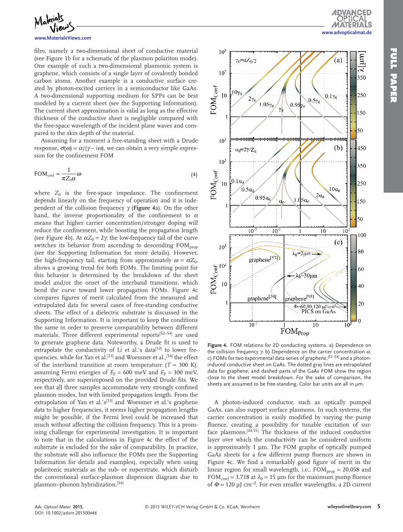
fi lm, namely a two-dimensional sheet of conductive material (see Figure 1 b for a schematic of the plasmon polariton mode). One example of such a two-dimensional plasmonic system is graphene, which consists of a single layer of covalently bonded carbon atoms. Another example is a conductive surface cre-ated by photon-excited carriers in a semiconductor like GaAs. A two-dimensional supporting medium for SPPs can be best modeled by a current sheet (see the Supporting Information). The current sheet approximation is valid as long as the effective thickness of the conductive sheet is negligible compared with the free-space wavelength of the incident plane waves and com-pared to the skin depth of the material.
Assuming for a moment a free-standing sheet with a Drude response, σ ( ω ) = α /( γ − i ω ), we can obtain a very simple expres-sion for the confi nement FOM
FOM1
conf0Zπ α
ω= (4)
where Z 0 is the free-space impedance. The confi nement depends linearly on the frequency of operation and it is inde-pendent of the collision frequency γ ( Figure 4 a). On the other hand, the inverse proportionality of the confi nement to α means that higher carrier concentration/stronger doping will reduce the confi nement, while boosting the propagation length (see Figure 4 b). At αZ 0 = 2 γ , the low-frequency tail of the curve switches its behavior from ascending to descending FOM prop (see the Supporting Information for more details). However, the high-frequency tail, starting from approximately ω = αZ 0 , shows a growing trend for both FOMs. The limiting point for this behavior is determined by the breakdown of the sheet model and/or the onset of the interband transitions, which bend the curve toward lower propagation FOMs. Figure 4 c compares fi gures of merit calculated from the measured and extrapolated data for several cases of free-standing conductive sheets. The effect of a dielectric substrate is discussed in the Supporting Information. It is important to keep the conditions the same in order to preserve comparability between different materials. Three different experimental reports [ 52–54 ] are used to generate graphene data. Noteworthy, a Drude fi t is used to extrapolate the conductivity of Li et al.’s data [ 52 ] to lower fre-quencies, while for Yan et al. [ 53 ] and Woessner et al., [ 54 ] the effect of the interband transition at room temperature ( T = 300 K), assuming Fermi energies of E F = 600 meV and E F = 300 meV, respectively, are superimposed on the provided Drude fi ts. We see that all three samples accommodate very strongly confi ned plasmon modes, but with limited propagation length. From the extrapolation of Yan et al.’s [ 53 ] and Woessner et al.’s graphene data to higher frequencies, it seems higher propagation lengths might be possible, if the Fermi level could be increased that much without affecting the collision frequency. This is a prom-ising challenge for experimental investigation. It is important to note that in the calculations in Figure 4 c the effect of the substrate is excluded for the sake of comparability. In practice, the substrate will also infl uence the FOMs (see the Supporting Information for details and examples), especially when using polaritonic materials as the sub- or superstrate, which disturb the conventional surface-plasmon dispersion diagram due to plasmon–phonon hybridization. [ 54 ]
A photon-induced conductor, such as optically pumped GaAs, can also support surface plasmons. In such systems, the carrier concentration is easily modifi ed by varying the pump fl uence, creating a possibility for tunable excitation of sur-face plasmons. [ 44,55 ] The thickness of the induced conductive layer over which the conductivity can be considered uniform is approximately 1 µm. The FOM graphs of optically pumped GaAs sheets for a few different pump fl uences are shown in Figure 4 c. We fi nd a remarkably good fi gure of merit in the linear region for small wavelength, i.e., FOM prop = 20.058 and FOM conf = 3.718 at λ 0 = 15 µm for the maximum pump fl uence of Φ = 120 µJ cm –2 . For even smaller wavelengths, a 2D current
Adv. Optical Mater. 2015, DOI: 10.1002/adom.201500446
Figure 4. FOM relations for 2D conducting systems. a) Dependence on the collision frequency γ . b) Dependence on the carrier concentration α . c) FOMs for two experimental data series of graphene, [ 52–54 ] and a photon-induced conductive sheet on GaAs. The dotted gray lines are extrapolated data for graphene, and dashed parts of the GaAs FOM show the region close to the sheet model breakdown. For the sake of comparison, the sheets are assumed to be free-standing. Color bar units are all in µm.
6 wileyonlinelibrary.com © 2015 WILEY-VCH Verlag GmbH & Co. KGaA, Weinheim
FULL
PAPER
FULL
PAPER
FULL
PAPER
www.MaterialsViews.comwww.advopticalmat.de
sheet can no longer accurately model the 1 µm thick current layer, as we will see in the following section.
2.4. Multi-interface Geometries
Figure 1 c,d demonstrates the most common multiple-interface geometries, known as the insulator–metal–insulator (IMI) and metal–insulator–metal (MIM) structures. For the sake of simplicity, we restrict ourselves to symmetric geometries. The presence of two interfaces results in hybridization of the single-interface SPPs to produce surface plasmons with symmetric and antisymmetric profi les, with respect to the parallel compo-nent of the electric fi eld, or, equivalently, the oscillating current direction at opposing interfaces. These modes display an eva-nescent character in the internal and the external media of the plasmonic waveguide. However, other types of bound modes that decay only into the external media with a propagating nature in between the interfaces may also exist (see also the Supporting Information). Such modes, referred to as guided modes, do not offer improved performance for plasmonic appli-cations, as can be seen from Figure 2 of the Supporting Informa-tion. Considering a source at −∞, in the presence of loss, causal solutions should decay toward +∞, implying Im( k || ) to be always positive. Such solutions can acquire either a positive or a nega-tive sign for Re( k || ) (dispersion relations in Figure 1 c,d). [ 56–58 ] In general, the average power fl ow is antiparallel to the phase fronts (Re( k || )) inside the metallic parts and along the phase fronts in the dielectric parts. However, the total energy fl ux along the interface follows the sign of Im( k || ) to obey causality. Figure 1 c,d shows the three modes with lowest dissipative loss for a generic Drude-type dielectric function.
2.5. Thin Films
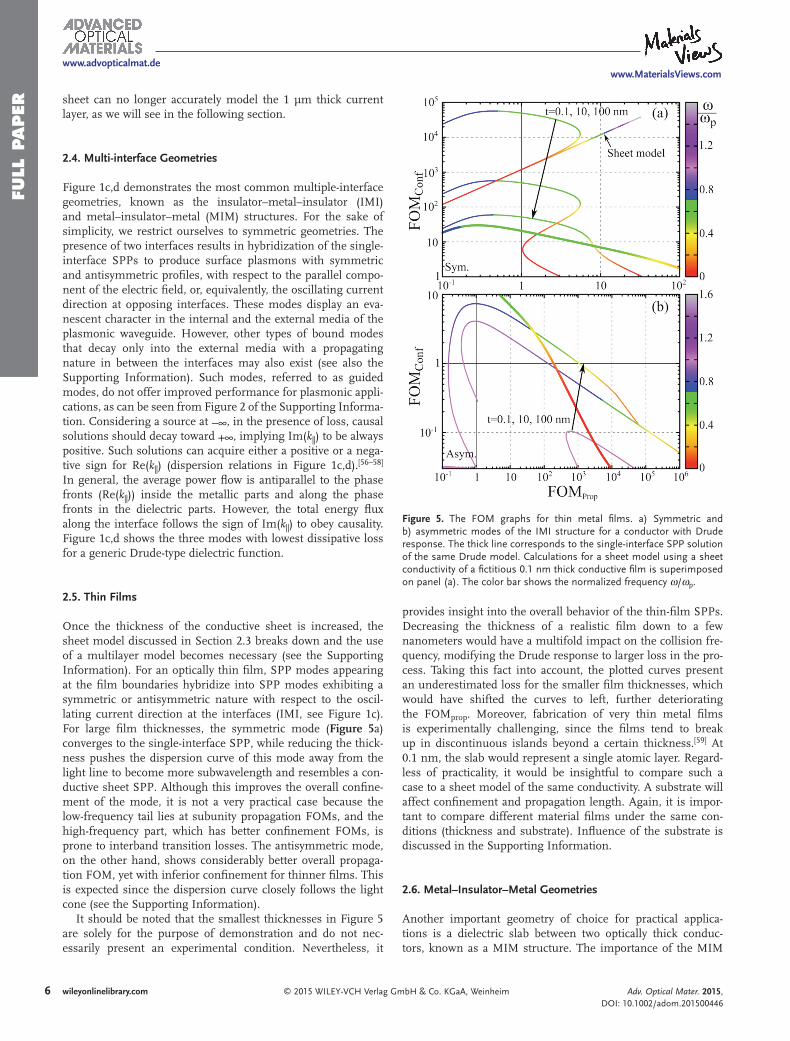
Once the thickness of the conductive sheet is increased, the sheet model discussed in Section 2.3 breaks down and the use of a multilayer model becomes necessary (see the Supporting Information). For an optically thin fi lm, SPP modes appearing at the fi lm boundaries hybridize into SPP modes exhibiting a symmetric or antisymmetric nature with respect to the oscil-lating current direction at the interfaces (IMI, see Figure 1 c). For large fi lm thicknesses, the symmetric mode ( Figure 5 a) converges to the single-interface SPP, while reducing the thick-ness pushes the dispersion curve of this mode away from the light line to become more subwavelength and resembles a con-ductive sheet SPP. Although this improves the overall confi ne-ment of the mode, it is not a very practical case because the low-frequency tail lies at subunity propagation FOMs, and the high-frequency part, which has better confi nement FOMs, is prone to interband transition losses. The antisymmetric mode, on the other hand, shows considerably better overall propaga-tion FOM, yet with inferior confi nement for thinner fi lms. This is expected since the dispersion curve closely follows the light cone (see the Supporting Information).
It should be noted that the smallest thicknesses in Figure 5 are solely for the purpose of demonstration and do not nec-essarily present an experimental condition. Nevertheless, it
provides insight into the overall behavior of the thin-fi lm SPPs. Decreasing the thickness of a realistic fi lm down to a few nanometers would have a multifold impact on the collision fre-quency, modifying the Drude response to larger loss in the pro-cess. Taking this fact into account, the plotted curves present an underestimated loss for the smaller fi lm thicknesses, which would have shifted the curves to left, further deteriorating the FOM prop . Moreover, fabrication of very thin metal fi lms is experimentally challenging, since the fi lms tend to break up in discontinuous islands beyond a certain thickness. [ 59 ] At 0.1 nm, the slab would represent a single atomic layer. Regard-less of practicality, it would be insightful to compare such a case to a sheet model of the same conductivity. A substrate will affect confi nement and propagation length. Again, it is impor-tant to compare different material fi lms under the same con-ditions (thickness and substrate). Infl uence of the substrate is discussed in the Supporting Information.
2.6. Metal–Insulator–Metal Geometries
Another important geometry of choice for practical applica-tions is a dielectric slab between two optically thick conduc-tors, known as a MIM structure. The importance of the MIM
Adv. Optical Mater. 2015, DOI: 10.1002/adom.201500446
Figure 5. The FOM graphs for thin metal fi lms. a) Symmetric and b) asymmetric modes of the IMI structure for a conductor with Drude response. The thick line corresponds to the single-interface SPP solution of the same Drude model. Calculations for a sheet model using a sheet conductivity of a fi ctitious 0.1 nm thick conductive fi lm is superimposed on panel (a). The color bar shows the normalized frequency ω / ω p .
7wileyonlinelibrary.com© 2015 WILEY-VCH Verlag GmbH & Co. KGaA, Weinheim
FULL P
APER
FULL P
APER
FULL P
APER
www.MaterialsViews.comwww.advopticalmat.de
Adv. Optical Mater. 2015, DOI: 10.1002/adom.201500446
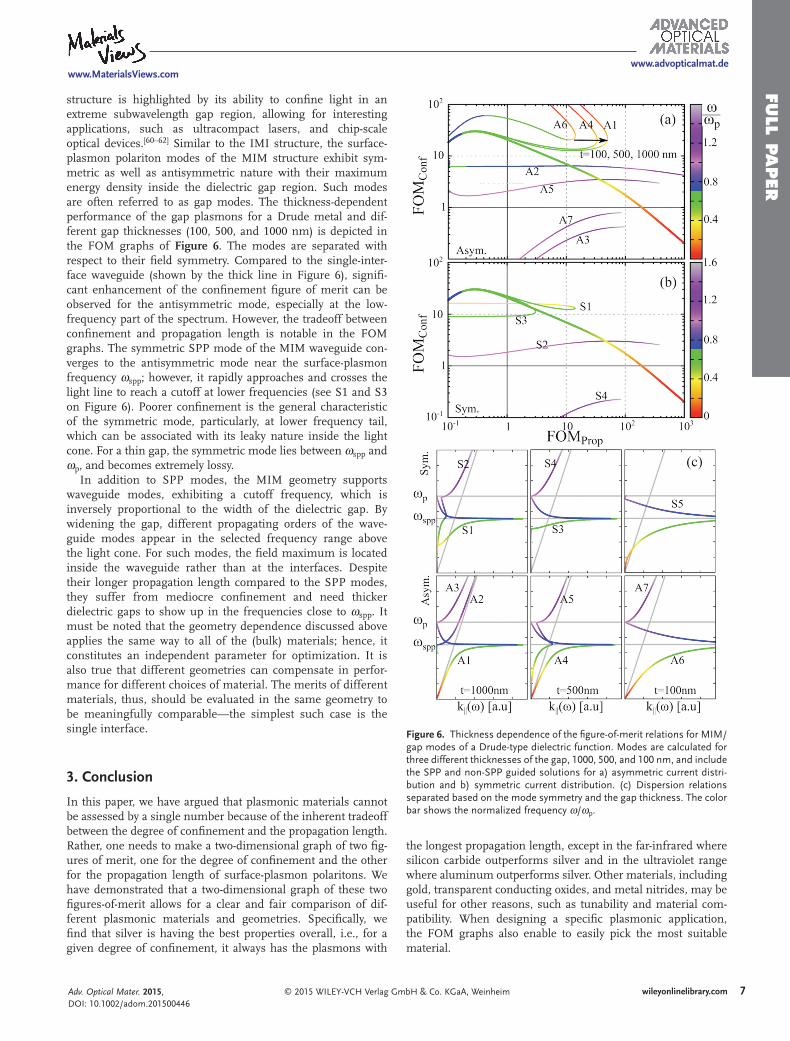
structure is highlighted by its ability to confi ne light in an extreme subwavelength gap region, allowing for interesting applications, such as ultracompact lasers, and chip-scale optical devices. [ 60–62 ] Similar to the IMI structure, the surface-plasmon polariton modes of the MIM structure exhibit sym-metric as well as antisymmetric nature with their maximum energy density inside the dielectric gap region. Such modes are often referred to as gap modes. The thickness-dependent performance of the gap plasmons for a Drude metal and dif-ferent gap thicknesses (100, 500, and 1000 nm) is depicted in the FOM graphs of Figure 6 . The modes are separated with respect to their fi eld symmetry. Compared to the single-inter-face waveguide (shown by the thick line in Figure 6 ), signifi -cant enhancement of the confi nement fi gure of merit can be observed for the antisymmetric mode, especially at the low-frequency part of the spectrum. However, the tradeoff between confi nement and propagation length is notable in the FOM graphs. The symmetric SPP mode of the MIM waveguide con-verges to the antisymmetric mode near the surface-plasmon frequency ω spp ; however, it rapidly approaches and crosses the light line to reach a cutoff at lower frequencies (see S1 and S3 on Figure 6 ). Poorer confi nement is the general characteristic of the symmetric mode, particularly, at lower frequency tail, which can be associated with its leaky nature inside the light cone. For a thin gap, the symmetric mode lies between ω spp and ω p , and becomes extremely lossy.
In addition to SPP modes, the MIM geometry supports waveguide modes, exhibiting a cutoff frequency, which is inversely proportional to the width of the dielectric gap. By widening the gap, different propagating orders of the wave-guide modes appear in the selected frequency range above the light cone. For such modes, the fi eld maximum is located inside the waveguide rather than at the interfaces. Despite their longer propagation length compared to the SPP modes, they suffer from mediocre confi nement and need thicker dielectric gaps to show up in the frequencies close to ω spp . It must be noted that the geometry dependence discussed above applies the same way to all of the (bulk) materials; hence, it constitutes an independent parameter for optimization. It is also true that different geometries can compensate in perfor-mance for different choices of material. The merits of different materials, thus, should be evaluated in the same geometry to be meaningfully comparable—the simplest such case is the single interface.
3. Conclusion
In this paper, we have argued that plasmonic materials cannot be assessed by a single number because of the inherent tradeoff between the degree of confi nement and the propagation length. Rather, one needs to make a two-dimensional graph of two fi g-ures of merit, one for the degree of confi nement and the other for the propagation length of surface-plasmon polaritons. We have demonstrated that a two-dimensional graph of these two fi gures-of-merit allows for a clear and fair comparison of dif-ferent plasmonic materials and geometries. Specifi cally, we fi nd that silver is having the best properties overall, i.e., for a given degree of confi nement, it always has the plasmons with
the longest propagation length, except in the far-infrared where silicon carbide outperforms silver and in the ultraviolet range where aluminum outperforms silver. Other materials, including gold, transparent conducting oxides, and metal nitrides, may be useful for other reasons, such as tunability and material com-patibility. When designing a specifi c plasmonic application, the FOM graphs also enable to easily pick the most suitable material.
Figure 6. Thickness dependence of the fi gure-of-merit relations for MIM/gap modes of a Drude-type dielectric function. Modes are calculated for three different thicknesses of the gap, 1000, 500, and 100 nm, and include the SPP and non-SPP guided solutions for a) asymmetric current distri-bution and b) symmetric current distribution. (c) Dispersion relations separated based on the mode symmetry and the gap thickness. The color bar shows the normalized frequency ω / ω p .
8 wileyonlinelibrary.com © 2015 WILEY-VCH Verlag GmbH & Co. KGaA, Weinheim
FULL
PAPER
FULL
PAPER
FULL
PAPER
www.MaterialsViews.comwww.advopticalmat.de
Adv. Optical Mater. 2015, DOI: 10.1002/adom.201500446
Supporting Information Supporting Information is available from the Wiley Online Library or from the author.
Acknowledgements Work at Ames Laboratory was partially supported by the U.S. Department of Energy, Offi ce of Basic Energy Science, Division of Materials Science and Engineering (Ames Laboratory is operated for the U.S. Department of Energy by Iowa State University under contract No. DE-AC02-07CH11358), by the U.S. Offi ce of Naval Research, award No. N00014-14-1-0474 (simulations). The European Research Council under the ERC Advanced Grant No. 320081 (PHOTOMETA) supported work (theory) at FORTH.
Received: August 9, 2015 Published online:
[1] J. Zenneck , Ann. Phys. 1907 , 328 , 846 . [2] A. Sommerfeld , Ann. Phys. 1909 , 333 , 665 . [3] A. Otto , Z. Phys. 1968 , 216 , 398 . [4] A. Otto , Z. Phys. 1969 , 219 , 227 . [5] E. N. Economou , Phys. Rev. 1969 , 182 , 539 . [6] E. Kretschmann , Z. Phys. 1971 , 241 , 313 . [7] A. D. Boardman , Electromagnetic Surface Modes , John Wiley & Sons
Ltd , Chichester 1982 . [8] V. M. Agranovich , D. L. Mills , Surface Polaritons: Electromagnetic
Waves at Surfaces and Interfaces , North-Holland , Amsterdam 1982 . [9] W. L. Barnes , A. Dereux , T. W. Ebbesen , Nature 2003 , 424 , 824 .
[10] W. L. Barnes , J. Opt. A: Pure Appl. Opt. 2006 , 8 , S87 . [11] S. A. Maier , Plasmonics: Fundamentals and Applications , Springer,
Boston, MA 2007 . [12] A. V. Zayats , I. I. Smolyaninov , A. A. Maradudin , Phys. Rep. 2005 ,
408 , 131 . [13] S. A. Maier , H. A. Atwater , J. Appl. Phys. 2005 , 98 , 011101 . [14] E. Ozbay , Science 2006 , 311 , 189 . [15] D. K. Gramotnev , S. I. Bozhevolnyi , Nat. Photonics 2010 , 4 , 83 . [16] M. Stockman , Phys. Rev. Lett. 2004 , 93 , 137404 . [17] A. J. Haes , R. P. Van Duyne , J. Am. Chem. Soc. 2002 , 124 , 10596 . [18] S. Lal , S. Link , N. J. Halas , Nat. Photonics 2007 , 1 , 641 . [19] P. Berini , I. De Leon , Nat. Photonics 2011 , 6 , 16 . [20] M. Kauranen , A. V. Zayats , Nat. Photonics 2012 , 6 , 737 . [21] K. R. Catchpole , A. Polman , Opt. Express 2008 , 16 , 21793 . [22] A. Boltasseva , T. Nikolajsen , K. Leosson , K. Kjaer , M. S. Larsen ,
S. I. Bozhevolnyi , J. Light. Technol. 2005 , 23 , 413 . [23] R. Zia , J. A. Schuller , A. Chandran , M. L. Brongersma , Mater. Today
2006 , 9 , 20 . [24] J. A. Conway , S. Sahni , T. Szkopek , Opt. Express 2007 , 15 , 4474 . [25] W. Cai , J. S. White , M. L. Brongersma , Nano Lett. 2009 , 9 , 4403 . [26] J. B. Khurgin , G. Sun , Appl. Phys. Lett. 2011 , 99 , 211106 . [27] P. Berini , Adv. Opt. Photonics 2009 , 1 , 484 . [28] D. K. Gramotnev , D. F. P. Pile , Appl. Phys. Lett. 2004 , 85 , 6323 . [29] D. A. Bobb , G. Zhu , M. Mayy , A. V. Gavrilenko , P. Mead ,
V. I. Gavrilenko , M. A. Noginov , Appl. Phys. Lett. 2009 , 95 , 151102 .
[30] M. G. Blaber , M. D. Arnold , M. J. Ford , J. Phys. Condens. Matter 2010 , 22 , 095501 .
[31] P. R. West , S. Ishii , G. V. Naik , N. K. Emani , V. M. Shalaev , A. Boltasseva , Laser Photon. Rev. 2010 , 4 , 795 .
[32] A. Boltasseva , H. A. Atwater , Science 2011 , 331 , 290 . [33] G. V. Naik , J. Kim , A. Boltasseva , Opt. Mater. Express 2011 , 1 , 1090 . [34] G. V. Naik , A. Boltasseva , Metamaterials 2011 , 5 , 1 . [35] M. Jablan , H. Buljan , M. Solja i , Phys. Rev. B 2009 , 80 , 1 . [36] A. Vakil , N. Engheta , Science 2011 , 332 , 1291 . [37] F. H. L. Koppens , D. E. Chang , F. J. García de Abajo , Nano Lett.
2011 , 11 , 3370 . [38] J. Horng , C.-F. Chen , B. Geng , C. Girit , Y. Zhang , Z. Hao ,
H. A. Bechtel , M. Martin , A. Zettl , M. F. Crommie , Y. R. Shen , F. Wang , Phys. Rev. B 2011 , 83 , 165113 .
[39] P. Tassin , T. Koschny , C. M. Soukoulis , Science 2013 , 341 , 620 . [40] R. Zia , M. D. Selker , P. B. Catrysse , M. L. Brongersma , J. Opt. Soc.
Am. A 2004 , 21 , 2442 . [41] R. F. Oulton , G. Bartal , D. F. P. Pile , X. Zhang , New J. Phys. 2008 ,
10 , 105018 . [42] P. Berini , Opt. Express 2006 , 14 , 13030 . [43] G. V Naik , N. K. Emani , U. Guler , A. Boltasseva , IEEE J. Sel. Top.
Quantum Electron. 2013 , 19 , 4601907 . [44] M. Beard , G. Turner , C. Schmuttenmaer , Phys. Rev. B 2000 , 62 ,
15764 . [45] E. Feigenbaum , K. Diest , H. A. Atwater , Nano Lett. 2010 , 10 , 2111 . [46] V. W. Brar , M. S. Jang , M. Sherrott , J. J. Lopez , H. A. Atwater , Nano
Lett. 2013 , 13 , 2541 . [47] A. D. Rakic , A. B. Djurišic , J. M. Elazar , M. L. Majewski , Appl. Opt.
1998 , 37 , 5271 . [48] P. B. Johnson , R. W. Christy , Phys. Rev. B 1972 , 6 , 4370 . [49] E. D. Palik , Handbook of Optical Constants of Solids , Academic Press ,
San Diego 1998 . [50] G. V Naik , V. M. Shalaev , A. Boltasseva , Adv. Mater. 2013 , 25 , 3264 . [51] M. A. Ordal , R. J. Bell , R. W. Alexander Jr. , L. L. Long , M. R. Querry ,
Appl. Opt. 1985 , 24 , 4493 . [52] Z. Q. Li , E. A. Henriksen , Z. Jiang , Z. Hao , M. C. Martin , P. Kim ,
H. L. Stormer , D. N. Basov , Nat. Phys. 2008 , 4 , 532 . [53] H. Yan , X. Li , B. Chandra , G. Tulevski , Y. Wu , M. Freitag , W. Zhu ,
P. Avouris , F. Xia , Nat. Nanotechnol. 2012 , 7 , 330 . [54] A. Woessner , M. B. Lundeberg , Y. Gao , A. Principi , P. Alonso-González ,
M. Carrega , K. Watanabe , T. Taniguchi , G. Vignale , M. Polini , J. Hone , R. Hillenbrand , F. H. L. Koppens , Nat. Mater. 2014 , 14 , 421 .
[55] I. Chatzakis , P. Tassin , L. Luo , N.-H. Shen , L. Zhang , J. Wang , T. Koschny , C. M. Soukoulis , Appl. Phys. Lett. 2013 , 103 , 043101 .
[56] E. Feigenbaum , N. Kaminski , M. Orenstein , Opt. Express 2009 , 17 , 18934 .
[57] A. R. Davoyan , I. V Shadrivov , Y. S. Kivshar , Opt. Express 2008 , 16 , 21209 .
[58] A. Davoyan , J. Nanophotonics 2010 , 4 , 043509 . [59] F. Moresco , M. Rocca , T. Hildebrandt , M. Henzler , Phys. Rev. Lett.
1999 , 83 , 2238 . [60] H. Miyazaki , Y. Kurokawa , Phys. Rev. Lett. 2006 , 96 , 097401 . [61] M. T. Hill , M. Marell , E. S. P. Leong , B. Smalbrugge , Y. Zhu , M. Sun ,
P. J. van Veldhoven , E. J. Geluk , F. Karouta , Y.-S. Oei , R. Nötzel , C.-Z. Ning , M. K. Smit , Opt. Express 2009 , 17 , 11107 .
[62] J. A. Dionne , K. Diest , L. A. Sweatlock , H. A. Atwater , Nano Lett. 2009 , 9 , 897 .