Embed Size (px)
Citation preview
1108 IEEE TRANSACTIONS ON ELECTRON DEVICES, VOL. 51, NO. 7, JULY 2004
A New Trench Bipolar Transistor for RF ApplicationsRaymond J. E. Hueting, Member, IEEE, Jan W. Slotboom, Member, IEEE, Joost Melai, Prabhat Agarwal, and
Peter H. C. Magnée
Abstract—A new vertical trench SiGe heterojunction bipolartransistor (HBT) is proposed that improves the tradeoff betweenthe cutoff frequency ( ) and the off-state collector-base break-down voltage (BVcbo). Extensive device simulations show that arecord BVcbo product of about 2375 GHz V can be obtainedfor an HBT having a trench field plate connected to the emitter anda linearly graded doping profile in the collector drift region, whileabout 700 GHz V can be obtained for a standard optimized HBT.This large improvement is explained mainly by the suppression ofthe base-widening effect.
Index Terms—Heterojunction bipolar transistors (HBTs), HFamplifiers, power semiconductor devices, silicon compounds,simulation.
I. INTRODUCTION
S iGe BiCMOS technology is important for high-frequencyapplications such as optical data communication operating
at 10 and 40 Gb/s [1]–[3]. For RF power applications suchas cellular phones SiGe HBTs are also important [1], [4].Generally, it is appreciated to have a transistor that is capableof blocking higher voltages while maintaining its good RFperformance.
It is well known that for a high-voltage (HV) transistor, thetradeoff between the drift resistance and the breakdown voltageis improved by the reduced surface field (RESURF) effect [5].The idea is to reshape the electric field distribution in the col-lector drift region for a reverse bias situation such that a moreuniform field distribution with a reduced maximal field isformed. The BV of the device is thereby increased and al-ternatively, for the same BV the doping concentration caneffectively be increased yielding a reduced collector resistance
. Another type of RESURF effect as proposed earlier [6] isshown in Fig. 1. The lateral p -n-n diode shown here is typ-ically used in any power device, such as bipolar transistors orMOSFETs, where the p -type layer represents the base or back-gate and the n-type layer the collector or drain. Underneath thediode is a field plate (FP), in this case the substrate, adjacent to alinearly graded doping profile in the drift region. The FP is iso-lated by a thick dielectric layer. The combination of the gradeddoping profile and the FP induces a lateral variation in depletioncapacitance between the drift region and substrate for a reversebiased situation and is used to reshape the electric field. Since alinearly graded profile is used a uniform field distribution can be
Manuscript received December 2, 2003; revised March 18, 2004. The reviewof this paper was arranged by Editor M.-C. Chang.
R. J. E. Hueting, J. Melai, P. Agarwal, and P. H. C. Magnée are with PhilipsResearch, Leuven B-3001, Belgium.
J. W. Slotboom is with the DIMES, Delft University of Technology, Delft2628 CT, The Netherlands (e-mail: [email protected]).
Digital Object Identifier 10.1109/TED.2004.829867
Fig. 1. Schematic drawing of an originally proposed RESURF device concept[6]. The n substrate is used as a FP and a linearly graded doping profileN(x) = N +� �x is used in the drift region of a p -n-n diode.W indicatesthe depletion layer width at the surface. The dashed lines represent the edgesof the depletion layer region.
obtained at the silicon surface [6]. This graded profile should bedesigned such that the collector resistance is reduced, e.g.,it has a high doping concentration at the base–collector (BC)junction and an increasing steep slope toward the collector con-tact. The collector resistance can be reduced more by usingtwo FPs instead of one, i.e., double RESURF effect, where thesecond FP is located at the silicon surface. Also, in vertical de-vices this (double) RESURF effect can be obtained by using FPfilled trenches [7]. Experimental evidence of this effect by usingthese FP filled trenches was reported in [8] for trench MOS bar-rier Schottky rectifiers.
In this paper, we show that by using the RESURF effect thebase widening effect in a bipolar transistor [9] is suppressed.This base widening effect limits the maximal in the tran-sistor and, hence, by using the RESURF effect the BVproduct is improved. Our device simulations show for a ver-tical npn SiGe HBT having a FP in a trench located along alinearly graded doping profile, a record BV product of95 GHz V GHz V can be obtained. Since for RFpower the BV is of greater importance than the open-basebreakdown voltage BV , we focus on the BV and . Atypical BV value for RF power devices is around 25 V [4].
II. DEVICE STRUCTURES
The emitter and base profile used in this paper were opti-mized for a 160 GHz HBT [10]. The base has a top dopingconcentration of 5 cm and is 130 wide. The Gepercentage of the uniform Ge profile is 20%. The 150 wide
-type lightly doped emitter has a doping concentration of2 cm . Three HV devices were evaluated which have thesame emitter and base profile but a different collector profilefor the same BV of 25 V. The first device, the standard HBT,has a uniform doping concentration of 2.1 cm and a
0018-9383/04$20.00 © 2004 IEEE
HUETING et al.: NEW TRENCH BIPOLAR TRANSISTOR FOR RF APPLICATIONS 1109
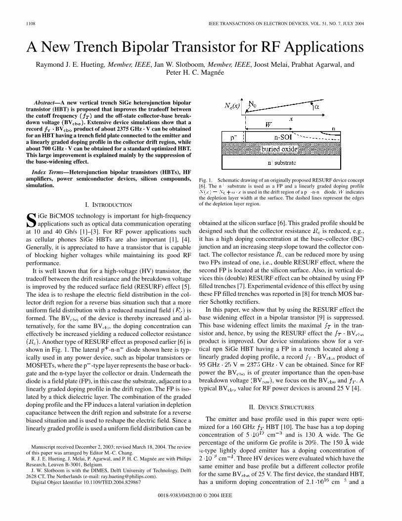
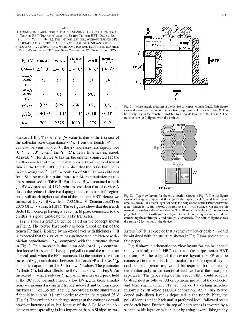
Fig. 2. Schematic drawing of the trench SiGe HBT (right) and the verticaldoping profile in the drift region (left). Half of the device structure isconveniently drawn from the axis of symmetry. The emitter (E), base (B) andcollector (C) are indicated in the figure. The dotted area indicates the SiGelayer. The thickness of the oxide layer (t ) is 0.135 �m and the width m=2 is0.125 �m. The FP can be connected to the base, emitter or a separate terminal.The dashed line represents the edge of the depletion layer region.
TABLE IDEVICE PARAMETERS FOR THREE HBTS: THE STANDARD HBT, THE
HEXAGONAL TRENCH HBT (DEVICE A) AND THE STRIPE TRENCH HBT(DEVICE B). THE DEVICE PARAMETERS ARE INDICATED IN FIGS. 1 AND 2
drift length of 1 m. The first RESURF or trench HBT(device A) has a linearly graded doping profile with a dopingconcentration of 4 cm at the BC junction and aslope of 9 cm (Fig. 2). The trench FP is isolated fromthe drift region by a 135-nm-thick oxide layer. This thick oxidelayer is also in the trench bottom in order to prevent oxidebreakthrough during reverse bias operation. Furthermore, thisHBT has a hexagonal (or cylindrical) geometry. The secondtrench HBT (device B) has a stripe (two-dimensional) geometryand because the effect of the FP on the drift region is lesscompared with device A, different device parameters have beenused. More details about the device structures can be found inTable I.
III. RESULTS AND DISCUSSION
All devices were optimized for 25 V BV by using thedevice simulator MEDICI [11]. For the transport parametersin the SiGe base we used values as proposed in [12]. Theseparameters are important for on-state simulations, such as for
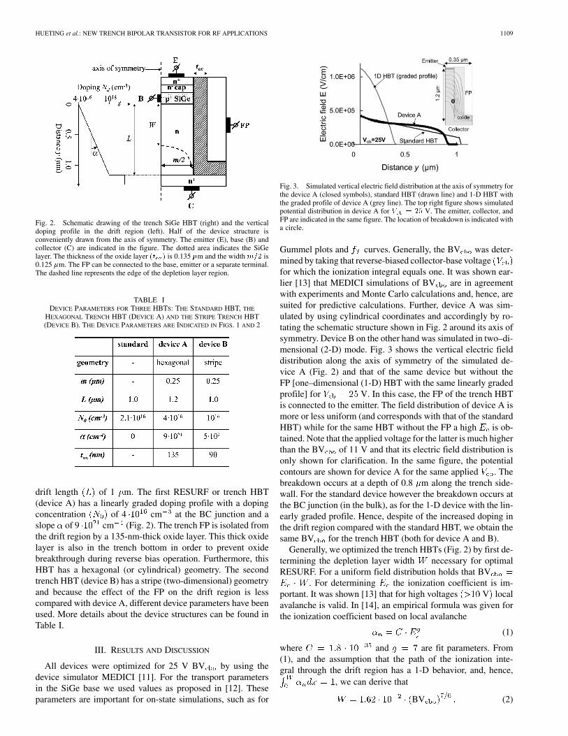
Fig. 3. Simulated vertical electric field distribution at the axis of symmetry forthe device A (closed symbols), standard HBT (drawn line) and 1-D HBT withthe graded profile of device A (grey line). The top right figure shows simulatedpotential distribution in device A for V = 25 V. The emitter, collector, andFP are indicated in the same figure. The location of breakdown is indicated witha circle.
Gummel plots and curves. Generally, the BV was deter-mined by taking that reverse-biased collector-base voltagefor which the ionization integral equals one. It was shown ear-lier [13] that MEDICI simulations of BV are in agreementwith experiments and Monte Carlo calculations and, hence, aresuited for predictive calculations. Further, device A was sim-ulated by using cylindrical coordinates and accordingly by ro-tating the schematic structure shown in Fig. 2 around its axis ofsymmetry. Device B on the other hand was simulated in two–di-mensional (2-D) mode. Fig. 3 shows the vertical electric fielddistribution along the axis of symmetry of the simulated de-vice A (Fig. 2) and that of the same device but without theFP [one–dimensional (1-D) HBT with the same linearly gradedprofile] for V. In this case, the FP of the trench HBTis connected to the emitter. The field distribution of device A ismore or less uniform (and corresponds with that of the standardHBT) while for the same HBT without the FP a high is ob-tained. Note that the applied voltage for the latter is much higherthan the BV of 11 V and that its electric field distribution isonly shown for clarification. In the same figure, the potentialcontours are shown for device A for the same applied . Thebreakdown occurs at a depth of 0.8 m along the trench side-wall. For the standard device however the breakdown occurs atthe BC junction (in the bulk), as for the 1-D device with the lin-early graded profile. Hence, despite of the increased doping inthe drift region compared with the standard HBT, we obtain thesame BV for the trench HBT (both for device A and B).
Generally, we optimized the trench HBTs (Fig. 2) by first de-termining the depletion layer width necessary for optimalRESURF. For a uniform field distribution holds that BV
. For determining the ionization coefficient is im-portant. It was shown [13] that for high voltages V localavalanche is valid. In [14], an empirical formula was given forthe ionization coefficient based on local avalanche
(1)
where and are fit parameters. From(1), and the assumption that the path of the ionization inte-gral through the drift region has a 1-D behavior, and, hence,
, we can derive that
BV (2)
1110 IEEE TRANSACTIONS ON ELECTRON DEVICES, VOL. 51, NO. 7, JULY 2004
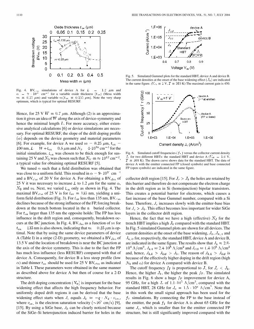
Fig. 4. BV simulations of device A for L = 1:2 �m and� = 9 � 10 cm for a variable oxide thickness (t ) (Mesa widthm = 0:25 �m) and variable m(t = 0:135 �m). Note the very sharpoptimum, which is typical for optimal RESURF.
Hence, for 25 V m. Although (2) is an approxima-tion it gives an idea of along the axis of device-symmetry andhence the minimal length . For more accuracy, either exten-sive analytical calculations [6] or device simulations are neces-sary. For optimal RESURF, the slope of the drift doping profile
depends on the device geometry and material parameters[6]. For example, for device A we used m,
nm, m and cm for theinitial simulations. was chosen to be thick enough for sus-taining 25 V and was chosen such that m cm ,a typical value for obtaining optimal RESURF [5].
We tuned such that a field distribution was obtained thatwas close to a uniform field. This resulted in cmand a BV of 20 V for device A. For obtaining a BV of25 V it was necessary to increase to 1.2 m for the same ,
and . Next, we varied only as shown in Fig. 4. Themaximal BV of 25 V is for nm, yielding a uni-form field distribution (Fig. 3). For less than 135 nm, BVdeclines because of the strong influence of the FP, forcing break-down at the trench bottom located in the n buried collector.For larger than 135 nm the opposite holds: The FP has lessinfluence in the drift region and, consequently, breakdown oc-curs at the BC junction. In Fig. 4, BV as a function of for
nm is also shown, indicating that m is op-timal. Note that by using the same device parameters of deviceA (Table I) in a stripe (2-D) geometry, we obtained a BV of13.5 V and the location of breakdown is near the BC junction atthe axis of the device symmetry. This is due to the fact the FPhas much less influence (less RESURF) compared with that ofdevice A. Consequently, for device B a less steep profile (low
) and thinner should be used for 25 V BV as indicatedin Table I. These parameters were obtained in the same manneras described above for device A but then of course for a 2-Dstructure.
The drift doping concentration is important for the basewidening effect that affects the high frequency behavior. Foruniformly doped drift regions it can be derived that the basewidening effect starts when equals ,where is the electron saturation velocity cm s [9],[15]. By using a SiGe base, can be clearly noticed becauseof the SiGe–Si heterojunction induced barrier for holes in the
Fig. 5. Simulated Gummel plots for the standard HBT, device A and device B.The current densities at the onset of the base widening effect (J ) are indicatedin the same figure. (V = 1 V, T = 300 K) The maximal current gain is 450.
Fig. 6. Simulated cutoff frequencies (f ) versus the collector current densityJ for two different HBTs: the standard HBT and device A (V = 1:0 V,T = 300 K). The drawn curve shows data for the standard HBT. The data ofdevice A with the emitter connected FP (closed symbols) and base connectedFP (open symbols) are indicated in the same figure.
collector drift region [15]. For the holes are retained bythis barrier and therefore do not compensate the electron chargein the drift region as in Si (homojunction) bipolar transistors.This creates a potential barrier for electrons, which causes afast increase of the base Gummel number, compared with a Sibase. Therefore, increases slowly with the emitter-base biasfor . This effect becomes less important for wider SiGelayers in the collector drift region.
Hence, the fact that we have a high (effective) for thetrench HBT implies a high compared with the standard HBT.In Fig. 5 simulated Gummel plots are shown for all devices. Thecurrent densities at the onset of the base widening, , and
for, respectively, the standard HBT, device A and device B,are indicated in the same figure. The results show that
cm , cm and cmand, hence, . The reason of isbecause of the effectively higher doping in the drift region (high
and ) for device A compared with device B.The cutoff frequency is proportional to for .
Hence, the higher , the higher the peak . The simulatedresults in Fig. 6 show a huge improvement for device A,95 GHz, for a high of 1.1 cm , compared with thestandard HBT, 28 GHz for cm . Note thatin this work the small signal approach has been used for the
simulations. By connecting the FP to the base instead ofthe emitter, the peak for device A is about 65 GHz for thesame , which is smaller than for the emitter connected FPstructure, but is still significantly improved compared with the
HUETING et al.: NEW TRENCH BIPOLAR TRANSISTOR FOR RF APPLICATIONS 1111
TABLE IIOBTAINED SIMULATED RESULTS FOR THE STANDARD HBT, THE HEXAGONAL
TRENCH HBT (DEVICE A) AND THE STRIPE TRENCH HBT (DEVICE B).(V = 1 V, T = 300 K). THE 1-D RESULTS (I.E., WITHOUT TRENCH FP)
OBTAINED FOR DEVICE A AND DEVICE B ARE ALSO SHOWN. CUT-OFF
FREQUENCY (f ) SIMULATIONS WERE DONE FOR EMITTER CONNECTED FIELD
PLATE (DENOTED BY “E”) AND BASE CONNECTED FP (DENOTED BY “B”)
standard HBT. This smaller value is due to the increase ofthe collector-base capacitance from the trench FP. Thiscan also be seen for low : the increases less rapidly. For
cm the delay time has increased.At peak , for device A having the emitter connected FP, theemitter-base transit time contribution is 40% of the total transittime in the trench HBT. This implies that the SiGe base helpsin improving the [12]: a peak of 50 GHz was obtainedfor a Si base trench bipolar transistor. More simulation resultsare summarized in Table II. For device B we obtained a peak
BV product of 1775, what is less than that of device Adue to the reduced effective doping in the collector drift region,but is still much higher than that of the standard HBT. Hence, weincreased the BV from 700 GHz V (Standard HBT) to2375 GHz V (trench HBT). These figures show that the trenchSiGe HBT concept having a trench field plate connected to theemitter is a good candidate for a HV transistor.
Fig. 7 shows a practical device based on the concept shownin Fig. 2. The p-type base poly has been placed on top of thetrench FP that is isolated by an oxide layer with thickness . Itis expected that this structure has an increased emitter-base de-pletion capacitance compared with the structure shownin Fig. 2. This increase is due to an additional contribu-tion located between the base p polysilicon and the n emittersidewall and, when the FP is connected to the emitter, due to anincreased contribution between the trench FP and base.is mainly important for the for low values. The parameter
affects but also affects the BV , as shown in Fig. 9. Anincreased , which reduces , yields an increased peak fieldat the BC junction and, hence, a low BV . In these simula-tions we assumed a constant trench sidewall and bottom oxidethickness of 135 nm (Fig. 7). According to the simulations
should be at most 0.1 m in order to obtain the required 25 V(Fig. 9). The emitter-base charge storage at the emitter sidewallhowever increases also, but because of the SiGe base the col-lector current spreading is less important than in Si bipolar tran-
Fig. 7. More practical design of the device concept shown in Fig. 2. This figureshows the device cross section taken from, e.g., line AA shown in Fig. 8. Thebase poly lies on the trench FP isolated by an oxide layer with thickness d. Thetrenches are self-aligned with the emitter.
Fig. 8. Top-view layout for the cross section shown in Fig. 7. The top figureshows a hexagonal layout, at the edge of the layout the FP metal layer (grayarea) is shown. This metal layer connects the polysilicon of the FP trench (whitearea), which is locally moved upwards to the silicon surface, via the trenchnetwork throughout the whole device. The FP trench is isolated from the basepoly (hatched area) with an oxide layer. A double metal layer can be used forconnecting the emitter poly and base poly separately. The bottom figure showsthe stripe (2-D) layout of the device.
sistors [16], it is expected that a somewhat lower peak wouldbe obtained with the structure shown in Fig. 7 than presented inthis paper.
Fig. 8 shows a schematic top view layout for the hexagonal(or cylindrical) trench HBT (top) and the stripe trench HBT(bottom). At the edge of the device layout the FP can beconnected to the emitter. In particular for the hexagonal layoutdouble metal processing would be required for connectingthe emitter poly in the centre of each cell and the base polyseparately. The processing of the trench HBT could roughlybe described as follows. After epitaxial growth of the collectorand base region trench FPs are formed by etching trenchesfollowed by an oxide (TEOS) deposition. An in situ n-typedoped polysilicon layer is deposited in the trench. Next, thepolysilicon is etched back until a preferred level, followed by anoxide etch back. Further, the top of the trenches is covered by asecond oxide layer on which later by using several lithography
1112 IEEE TRANSACTIONS ON ELECTRON DEVICES, VOL. 51, NO. 7, JULY 2004
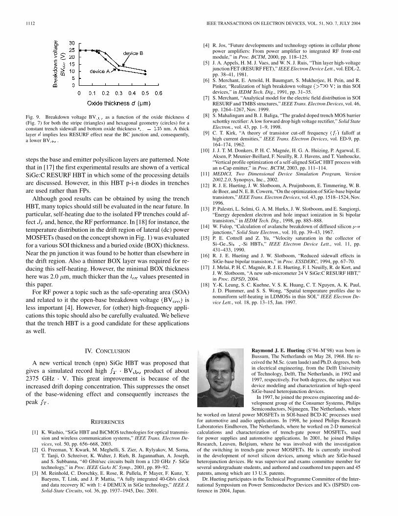
Fig. 9. Breakdown voltage BV as a function of the oxide thickness d
(Fig. 7) for both the stripe (triangles) and hexagonal geometry (circles) for aconstant trench sidewall and bottom oxide thickness t = 135 nm. A thicklayer d implies less RESURF effect near the BC junction and, consequently,a lower BV .
steps the base and emitter polysilicon layers are patterned. Notethat in [17] the first experimental results are shown of a verticalSiGe:C RESURF HBT in which some of the processing detailsare discussed. However, in this HBT p-i-n diodes in trenchesare used rather than FPs.
Although good results can be obtained by using the trenchHBT, many topics should still be evaluated in the near future. Inparticular, self-heating due to the isolated FP trenches could af-fect and, hence, the RF performance. In [18] for instance, thetemperature distribution in the drift region of lateral (dc) powerMOSFETs (based on the concept shown in Fig. 1) was evaluatedfor a various SOI thickness and a buried oxide (BOX) thickness.Near the pn junction it was found to be hotter than elsewhere inthe drift region. Also a thinner BOX layer was required for re-ducing this self-heating. However, the minimal BOX thicknesshere was 2.0 m, much thicker than the values presented inthis paper.
For RF power a topic such as the safe-operating area (SOA)and related to it the open-base breakdown voltage BV isless important [4]. However, for (other) high-frequency appli-cations this topic should also be carefully evaluated. We believethat the trench HBT is a good candidate for these applicationsas well.
IV. CONCLUSION
A new vertical trench (npn) SiGe HBT was proposed thatgives a simulated record high BV product of about2375 GHz V. This great improvement is because of theincreased drift doping concentration. This suppresses the onsetof the base-widening effect and consequently increases thepeak .
REFERENCES
[1] K. Washio, “SiGe HBT and BiCMOS technologies for optical transmis-sion and wireless communication systems,” IEEE Trans. Electron De-vices, vol. 50, pp. 656–668, 2003.
[2] G. Freeman, Y. Kwark, M. Meghelli, S. Zier, A. Rylyakov, M. Sorna,T. Tanji, O. Schreiver, K. Walter, J. Rieh, B. Jagannathan, A. Joseph,and S. Subbanna, “40 Gbit/sec circuits built from a 120 GHz f SiGetechnology,” in Proc. IEEE GaAs IC Symp., 2001, pp. 89–92.
[3] M. Reinhold, C. Dorschky, E. Rose, R. Pullela, P. Mayer, F. Kunz, Y.Baeyens, T. Link, and J. P. Mattia, “A fully integrated 40-Gb/s clockand data recovery IC with 1: 4 DEMUX in SiGe technology,” IEEE J.Solid-State Circuits, vol. 36, pp. 1937–1945, Dec. 2001.
[4] R. Jos, “Future developments and technology options in cellular phonepower amplifiers: From power amplifier to integrated RF front-endmodule,” in Proc. BCTM, 2000, pp. 118–125.
[5] J. A. Appels, H. M. J. Vaes, and W. N. J. Ruis, “Thin layer high-voltagejunction FET (RESURF FET),” IEEE Electron Device Lett., vol. EDL-2,pp. 38–41, 1981.
[6] S. Merchant, E. Arnold, H. Baumgart, S. Mukherjee, H. Pein, and R.Pinker, “Realization of high breakdown voltage (>700 V) in thin SOIdevices,” in IEDM Tech. Dig., 1991, pp. 31–35.
[7] S. Merchant, “Analytical model for the electric field distribution in SOIRESURF and TMBS structures,” IEEE Trans. Electron Devices, vol. 46,pp. 1264–1267, Nov. 1999.
[8] S. Mahalingam and B. J. Baliga, “The graded doped trench MOS barrierschottky rectifier: A low forward drop high voltage rectifier,” Solid StateElectron., vol. 43, pp. 1–9, 1998.
[9] C. T. Kirk, “A theory of transistor cut-off frequency (f ) falloff athigh current densities,” IEEE Trans. Electron Devices, vol. ED-9, pp.164–174, 1962.
[10] J. J. T. M. Donkers, P. H. C. Magnée, H. G. A. Huizing, P. Agarwal, E.Aksen, P. Meunier-Beillard, F. Neuilly, R. J. Havens, and T. Vanhoucke,“Vertical profile optimization of a self-aligned SiGeC HBT process withan n-Cap emitter,” in Proc. BCTM, 2003, pp. 111–114.
[11] MEDICI, Two Dimensional Device Simulation Program, Version2002.2.0, Synopsys, Inc., 2002.
[12] R. J. E. Hueting, J. W. Slotboom, A. Pruijmboom, E. Timmering, W. B.de Boer, and N. E. B. Cowern, “On the optimization of SiGe-base bipolartransistors,” IEEE Trans. Electron Devices, vol. 43, pp. 1518–1524, Nov.1996.
[13] P. Palestri, L. Selmi, G. A. M. Hurkx, J. W. Slotboom, and E. Sangiorgi,“Energy dependent electron and hole impact ionization in Si bipolartransistors,” in IEDM Tech. Dig., 1998, pp. 885–888.
[14] W. Fulop, “Calculation of avalanche breakdown of diffused silicon p-njunctions,” Solid State Electron., vol. 10, pp. 39–43, 1967.
[15] P. E. Cottrell and Z. Yu, “Velocity saturation in the collector ofSi–Ge Si -Si HBTs,” IEEE Electron Device Lett., vol. 11, pp.431–433, 1990.
[16] R. J. E. Hueting and J. W. Slotboom, “Reduced sidewall effects inSiGe-base bipolar transistors,” in Proc. ESSDERC, 1994, pp. 67–70.
[17] J. Melai, P. H. C. Magnée, R. J. E. Hueting, F. I. Neuilly, R. de Kort, andJ. W. Slotboom, “A new sub-micrometer 24 V SiGe:C RESURF HBT,”in Proc. ISPSD, 2004.
[18] Y.-K. Leung, S. C. Kuehne, V. S. K. Huang, C. T. Nguyen, A. K. Paul,J. D. Plummer, and S. S. Wong, “Spatial temperature profiles due tononuniform self-heating in LDMOSs in thin SOI,” IEEE Electron De-vice Lett., vol. 18, pp. 13–15, Jan. 1997.
Raymond J. E. Hueting (S’94–M’98) was born inBussum, The Netherlands on May 28, 1968. He re-ceived the M.Sc. (cum laude) and Ph.D. degrees, bothin electrical engineering, from the Delft Universityof Technology, Delft, The Netherlands, in 1992 and1997, respectively. For both degrees, the subject wasdevice modeling and characterization of high-speedSiGe-based heterojunction devices.
In 1997, he joined the process engineering and de-velopment group of the Consumer Systems, PhilipsSemiconductors, Nijmegen, The Netherlands, where
he worked on lateral power MOSFETs in SOI-based BCD-IC processes usedfor automotive and audio applications. In 1998, he joined Philips ResearchLaboratories Eindhoven, The Netherlands, where he worked on 2-D numericalcalculations and characterization of trench-gate power MOSFETs, usedfor power supplies and automotive applications. In 2001, he joined PhilipsResearch, Leuven, Belgium, where he was involved with the investigationof the switching in trench-gate power MOSFETs. He is currently involvedin the development of novel silicon devices, among which are SiGe-basedheterojunction devices. He was supervisor and exams committee member forseveral undergraduate students, and authored and coauthored ten papers and 45patents, among which are 13 U.S. patents.
Dr. Hueting participates in the Technical Programme Committee of the Inter-national Symposium on Power Semiconductor Devices and ICs (ISPSD) con-ference in 2004, Japan.
HUETING et al.: NEW TRENCH BIPOLAR TRANSISTOR FOR RF APPLICATIONS 1113
Jan W. Slotboom (M’82) was born in Utrecht,The Netherlands, on December 26, 1942. Hereceived the M.Sc. degree in electrical engineeringfrom the Technical University of Delft, Delft, TheNetherlands, in 1966, and the Ph.D. degree from theTechnical University of Eindhoven, Eindhoven, TheNetherlands, in 1977. His dissertation was on 2-Dnumerical device simulation of bipolar transistorsand pioneering experiments on bandgap narrowingin heavily doped silicon.
In 1967, he joined the Philips Research Laborato-ries, Eindhoven, where he worked on bipolar device modeling, numerical sim-ulation, and experimental silicon device physics. He was involved in the de-velopment of CCD memories for video applications and exploratory researchof high-density memories. He has authored and coauthored over 50 papers andholds 14 patents. Since 1994, he has been a part-time Professor with the MicroElectronics Center (DIMES), Technical University of Delft. His current researchactivities are on research of novel silicon devices (e.g., SiGe bipolar transistors),hot-carrier effects, and new memory cells.
Dr. Slotboom was a member of the Solid-State Devices Subcommittee ofthe IEDM in 1980, 1983, and 1984, respectively. He was Vice Chairman andChairman of International Arrangements for Europe of the IEDM. He has servedas a Program Subcommittee Member of the IEDM in 1991 and 1992 and of theBCTM’95 Conference. He has been a member of the Technical Program Com-mittee of the ESSDERC for the last six years.
Joost Melai was born in Nijmegen, the Netherlandson December 30, 1976. He received the B.Sc. degreein applied physics from the Hogeschool Enschede,Enschede, The Netherlands, in 2000.
In 2001, he joined Philips Research, Leuven,Belgium, where he has been working in the SiliconProcess Options Group. He is involved with researchon novel Silicon devices, focusing on SiGe HBTs.
Prabhat Agarwal was born in Hamburg, Germany,in 1972. He received the B.S. degree in physicsfrom Trinity College, University of Cambridge,Cambridge, U.K., in 1995. His Ph.D. thesis focusedon the magnetic mechanism of superconductivity insystems near quantum phase transitions.
After a year as a Graduate Student in TheoreticalPhysics at the École Normale Supérieure, Paris, he re-turned to Cambridge for experimental research at theCavendish Laboratories. Since 2000, he has been em-ployed by Philips Research Laboratories, Eindhoven,
The Netherlands, and later in Leuven, Belgium, in the area of semiconductor de-vice physics. His current interests include high-speed bipolar devices and newsemiconductor device architectures.
Peter H. C. Magnée was born in Vlissingen, TheNetherlands in 1969. He received the M.Sc. andPh.D. degrees in applied physics from the Universityof Groningen, The Netherlands, in 1991 and 1996,respectively.
In 1996 he joined Philips Research, Eindhoven,The Netherlands, where he worked in Si-basedbipolar transistors for wide-band and RF powerapplications. In 2000, he joined Philips Research,Leuven (PRLe), Leuven, Belgium. He is theProject Leader of the Advanced Bipolar/BiCMOS
Technology project, which focuses on different technology and device optionsbased on Si–SiGe heterojunction bipolar transistors.