Embed Size (px)
Citation preview
Application ReportSZZA031 - December 2001
1
A Nickel-Palladium-Gold Integrated Circuit Lead Finishand Its Potential for Solder-Joint Embrittlement
Donald Abbott, Douglas Romm, Bernhard Lange Standard Linear & Logic
ABSTRACT
This gold (Au) embrittlement study evaluates TI’s original four-layer nickel-palladium (NiPd)lead finish that was introduced in 1989 and TI’s nickel-palladium-gold (NiPdAu) lead finishthat replaced four-layer NiPd in 2001. Samples were prepared with three different Authicknesses for the NiPdAu components. The printed wiring board (PWB) finishes used wereorganic solderability preservative (OSP) and electroless nickel-gold (NiAu). The latter weremade with two different Au thicknesses. The goal was to understand the effect of Au from thecomponent finish and the PWB pad finish on Au embrittlement in the solder joint. A matrixof samples was built from the components and boards described above and exposed to 1000temperature cycles. Lead pull testing and metallurgical analysis of the solder joints wereperformed to determine if the variations in Au content, either from the lead or the board orboth, led to Au embrittlement of the solder joints.
The theoretical calculations (Appendix A) showed that 3 weight % Au would not be exceededin the solder-joint test. Based on the Au embrittlement literature, this predicts no solder-jointembrittlement would occur. The lead pull data showed no evidence of catastrophic drop insolder-joint strength that would be expected with Au embrittlement. The cross sections showno SnAu intermetallics in the bulk of the solder for the solder joints made with normalAu-thickness-range components and boards. Thin layers of SnAu intermetallics are seen atthe solder/component and solder/PWB interfaces. This is expected because intermetallicsform between Sn from the solder and Au from the PWB and component finishes. Only thesolder joints made with artificially high Au-thickness components and PWBs have theacicular SnAu intermetallics that have been shown to cause Au embrittlement in someinstances in the literature. The NiPdAu leadframe finished components investigated for thisapplicaton report showed no measurable Au embrittlement of the solder joint.
Contents
Introduction 3. . . . . . . . . . . . . . . . . . . . . . . . . . . . . . . . . . . . . . . . . . . . . . . . . . . . . . . . . . . . . . . . . . . . . . . . . . . . . Components and PWBs Tested 4. . . . . . . . . . . . . . . . . . . . . . . . . . . . . . . . . . . . . . . . . . . . . . . . . . . . . . . . . Test Matrix for Au Embrittlement 4. . . . . . . . . . . . . . . . . . . . . . . . . . . . . . . . . . . . . . . . . . . . . . . . . . . . . . . . Reflow Profile 5. . . . . . . . . . . . . . . . . . . . . . . . . . . . . . . . . . . . . . . . . . . . . . . . . . . . . . . . . . . . . . . . . . . . . . . . Board-Mount Equipment and Procedure 5. . . . . . . . . . . . . . . . . . . . . . . . . . . . . . . . . . . . . . . . . . . . . . . . . Theoretical Au Content Calculations 5. . . . . . . . . . . . . . . . . . . . . . . . . . . . . . . . . . . . . . . . . . . . . . . . . . . . . Predicted Au Content of Solder Joints Using Thickness Data for ICs and PWBs 5. . . . . . . . . . . . . . .
SZZA031
2 A Nickel-Palladium-Gold Integrated Circuit Lead Finish and Its Potential for Solder-Joint Embrittlement
Performance Measures and Results 6. . . . . . . . . . . . . . . . . . . . . . . . . . . . . . . . . . . . . . . . . . . . . . . . . . . . . . . Visual Appearance 6. . . . . . . . . . . . . . . . . . . . . . . . . . . . . . . . . . . . . . . . . . . . . . . . . . . . . . . . . . . . . . . . . . . . Lead Pull Test 7. . . . . . . . . . . . . . . . . . . . . . . . . . . . . . . . . . . . . . . . . . . . . . . . . . . . . . . . . . . . . . . . . . . . . . . . Lead Pull Data 7. . . . . . . . . . . . . . . . . . . . . . . . . . . . . . . . . . . . . . . . . . . . . . . . . . . . . . . . . . . . . . . . . . . . . . . . Observations From Lead Pull Results 8. . . . . . . . . . . . . . . . . . . . . . . . . . . . . . . . . . . . . . . . . . . . . . . . . . .
Statistical Analysis of Lead Pull Data 8. . . . . . . . . . . . . . . . . . . . . . . . . . . . . . . . . . . . . . . . . . . . . . . . . . . . . . Analysis of Variance (ANOVA) 8. . . . . . . . . . . . . . . . . . . . . . . . . . . . . . . . . . . . . . . . . . . . . . . . . . . . . . . . . . Box-and-Whisker Plots 9. . . . . . . . . . . . . . . . . . . . . . . . . . . . . . . . . . . . . . . . . . . . . . . . . . . . . . . . . . . . . . . . Summary of Statistical Analysis 11. . . . . . . . . . . . . . . . . . . . . . . . . . . . . . . . . . . . . . . . . . . . . . . . . . . . . . . .
Cross Sections of Solder Joints 11. . . . . . . . . . . . . . . . . . . . . . . . . . . . . . . . . . . . . . . . . . . . . . . . . . . . . . . . . . Sample 6: NiPdAu Standard Finish, PWB Standard NiAu Finish 11. . . . . . . . . . . . . . . . . . . . . . . . . . . . Sample 5: NiPd Lead Finish, PWB Standard NiAu Finish After Thermal Cycling 12. . . . . . . . . . . . . . Sample 7: NiPdAu 5× Au, PWB Standard NiAu Finish After Thermal Cycling 14. . . . . . . . . . . . . . . . . Sample 2: NiPdAu Standard Finish, PWB OSP Finish After Thermal Cycling 14. . . . . . . . . . . . . . . . . Sample 10: NiPdAu Standard Finish, 5× NiAu PWB With No Thermal Cycling 15. . . . . . . . . . . . . . . . Sample 12: NiPdAu 100× Au, PWB 5× Au Thickness After Thermal Cycling 16. . . . . . . . . . . . . . . . . Summary of Cross-Section Analysis 17. . . . . . . . . . . . . . . . . . . . . . . . . . . . . . . . . . . . . . . . . . . . . . . . . . . .
Summary and Conclusions 17. . . . . . . . . . . . . . . . . . . . . . . . . . . . . . . . . . . . . . . . . . . . . . . . . . . . . . . . . . . . . .
Acknowledgments 18. . . . . . . . . . . . . . . . . . . . . . . . . . . . . . . . . . . . . . . . . . . . . . . . . . . . . . . . . . . . . . . . . . . . . .
References 18. . . . . . . . . . . . . . . . . . . . . . . . . . . . . . . . . . . . . . . . . . . . . . . . . . . . . . . . . . . . . . . . . . . . . . . . . . . . .
Appendix A Calculations for Au Embrittlement Study 19. . . . . . . . . . . . . . . . . . . . . . . . . . . . . . . . . . . . . .
List of Figures
1 Structure for TI Four-Layer NiPd Finish 3. . . . . . . . . . . . . . . . . . . . . . . . . . . . . . . . . . . . . . . . . . . . . . . . . . 2 Structure for NiPdAu Finish 3. . . . . . . . . . . . . . . . . . . . . . . . . . . . . . . . . . . . . . . . . . . . . . . . . . . . . . . . . . . . 3 Reflow Profile for SnPbAg Solder Alloy 5. . . . . . . . . . . . . . . . . . . . . . . . . . . . . . . . . . . . . . . . . . . . . . . . . . 4 Cross Section of Solder Joint 6. . . . . . . . . . . . . . . . . . . . . . . . . . . . . . . . . . . . . . . . . . . . . . . . . . . . . . . . . . . 5 Lead Pull Results 7. . . . . . . . . . . . . . . . . . . . . . . . . . . . . . . . . . . . . . . . . . . . . . . . . . . . . . . . . . . . . . . . . . . . . 6 Lead Pull Results by Factor-Level Setting 9. . . . . . . . . . . . . . . . . . . . . . . . . . . . . . . . . . . . . . . . . . . . . . . . 7 Box-and-Whisker Plot for OSP Coating on PWB (No Au) 10. . . . . . . . . . . . . . . . . . . . . . . . . . . . . . . . . . 8 Box-and-Whisker Plot for Standard NiAu PWB 10. . . . . . . . . . . . . . . . . . . . . . . . . . . . . . . . . . . . . . . . . . . 9 Box-and-Whisker Plot for PWB With 5× Au (0.4 µ to 0.65 µ) 11. . . . . . . . . . . . . . . . . . . . . . . . . . . . . . . 10 Sample 6 After Thermal Cycling (The Dark Gray Matrix Is the Tin-Rich Phase,
While the Bright Phase Is the Lead-Rich Phase) 12. . . . . . . . . . . . . . . . . . . . . . . . . . . . . . . . . . . . . . . . . 11 Board Side of Sample 6 at 4000× After Thermal Cycling 12. . . . . . . . . . . . . . . . . . . . . . . . . . . . . . . . . . 12 Lead Side of Sample 6 at 4000× After Thermal Cycling 12. . . . . . . . . . . . . . . . . . . . . . . . . . . . . . . . . . . 13 Spectra of Cu, Ni, Au, and Sn Taken Along Line 1–2 in Figure 12 12. . . . . . . . . . . . . . . . . . . . . . . . . . 14 1000× Image of Sample 5 After Thermal Cycling 13. . . . . . . . . . . . . . . . . . . . . . . . . . . . . . . . . . . . . . . . . 15 Board Side of Sample 5 at 4000× After Thermal Cycling 13. . . . . . . . . . . . . . . . . . . . . . . . . . . . . . . . . . 16 4000× Image on the Lead Side of Sample 5 After Thermal Cycling 13. . . . . . . . . . . . . . . . . . . . . . . . . 17 Line Scan Along Line 1–2 in Figure 16 13. . . . . . . . . . . . . . . . . . . . . . . . . . . . . . . . . . . . . . . . . . . . . . . . . . 18 Sample 7 at 1000× After Thermal Cycling 14. . . . . . . . . . . . . . . . . . . . . . . . . . . . . . . . . . . . . . . . . . . . . . . 19 1000× Image of Sample 2 After Thermal Cycling 15. . . . . . . . . . . . . . . . . . . . . . . . . . . . . . . . . . . . . . . . .
SZZA031
3 A Nickel-Palladium-Gold Integrated Circuit Lead Finish and Its Potential for Solder-Joint Embrittlement
20 1000× Image of Sample 10, No Thermal Cycling 15. . . . . . . . . . . . . . . . . . . . . . . . . . . . . . . . . . . . . . . . . 21 Sample 10 at 4000× Board Side, No Thermal Cycling 15. . . . . . . . . . . . . . . . . . . . . . . . . . . . . . . . . . . . . 22 Sample 10 Lead Side at 4000×, No Thermal Cycling 16. . . . . . . . . . . . . . . . . . . . . . . . . . . . . . . . . . . . . . 23 Line Scan Along Line 1–2 in Figure 22 16. . . . . . . . . . . . . . . . . . . . . . . . . . . . . . . . . . . . . . . . . . . . . . . . . . 24 Sample 12 at 1000× After Thermal Cycling 16. . . . . . . . . . . . . . . . . . . . . . . . . . . . . . . . . . . . . . . . . . . . . . 25 Sample 12 Pad Side at 4000× After Thermal Cycling 16. . . . . . . . . . . . . . . . . . . . . . . . . . . . . . . . . . . . . 26 Sample 12 Lead Side at 4000× After Thermal Cycling 17. . . . . . . . . . . . . . . . . . . . . . . . . . . . . . . . . . . . 27 Line Scan Along Line 1–2 in Figure 26 17. . . . . . . . . . . . . . . . . . . . . . . . . . . . . . . . . . . . . . . . . . . . . . . . . .
List of Tables
1 Group Numbers for Each Variation Tested 4. . . . . . . . . . . . . . . . . . . . . . . . . . . . . . . . . . . . . . . . . . . . . . . . 2 Calculated Weight % Au in the Solder Joints for the Test Matrix 6. . . . . . . . . . . . . . . . . . . . . . . . . . . . . 3 ANOVA Results 8. . . . . . . . . . . . . . . . . . . . . . . . . . . . . . . . . . . . . . . . . . . . . . . . . . . . . . . . . . . . . . . . . . . . . . . A–1 XRD/EDX Data 19. . . . . . . . . . . . . . . . . . . . . . . . . . . . . . . . . . . . . . . . . . . . . . . . . . . . . . . . . . . . . . . . . . . . . . A–2 XRF/EDX Data 20. . . . . . . . . . . . . . . . . . . . . . . . . . . . . . . . . . . . . . . . . . . . . . . . . . . . . . . . . . . . . . . . . . . . . . A–3 Calculations for Boards 20. . . . . . . . . . . . . . . . . . . . . . . . . . . . . . . . . . . . . . . . . . . . . . . . . . . . . . . . . . . . . . . A–4 Calculations for Components 21. . . . . . . . . . . . . . . . . . . . . . . . . . . . . . . . . . . . . . . . . . . . . . . . . . . . . . . . . . A–5 Calculated Percentage of Au in the Solder Joints 21. . . . . . . . . . . . . . . . . . . . . . . . . . . . . . . . . . . . . . . . .
Introduction
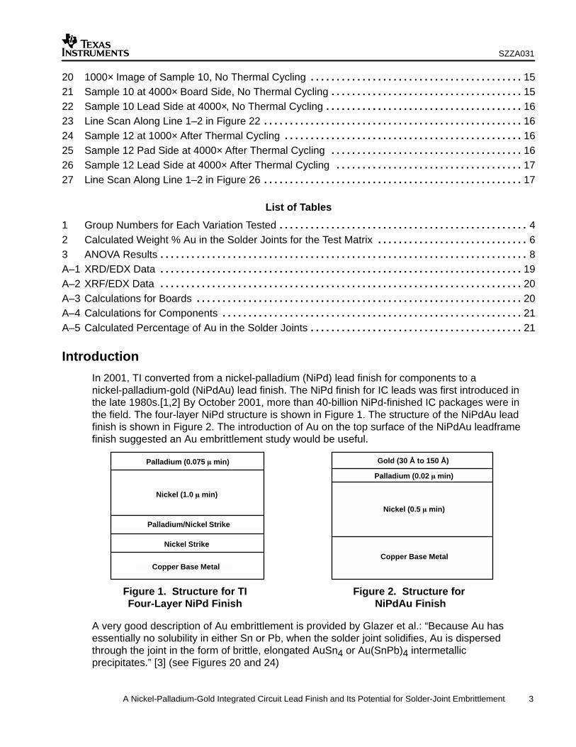
In 2001, TI converted from a nickel-palladium (NiPd) lead finish for components to anickel-palladium-gold (NiPdAu) lead finish. The NiPd finish for IC leads was first introduced inthe late 1980s.[1,2] By October 2001, more than 40-billion NiPd-finished IC packages were inthe field. The four-layer NiPd structure is shown in Figure 1. The structure of the NiPdAu leadfinish is shown in Figure 2. The introduction of Au on the top surface of the NiPdAu leadframefinish suggested an Au embrittlement study would be useful.
Copper Base Metal
Palladium (0.02 � min)
Gold (30 Å to 150 Å)
Nickel (0.5 � min)
Copper Base Metal
Nickel Strike
Palladium/Nickel Strike
Nickel (1.0 � min)
Palladium (0.075 � min)
Figure 1. Structure for TIFour-Layer NiPd Finish
Figure 2. Structure for NiPdAu Finish
A very good description of Au embrittlement is provided by Glazer et al.: “Because Au hasessentially no solubility in either Sn or Pb, when the solder joint solidifies, Au is dispersedthrough the joint in the form of brittle, elongated AuSn4 or Au(SnPb)4 intermetallicprecipitates.” [3] (see Figures 20 and 24)
SZZA031
4 A Nickel-Palladium-Gold Integrated Circuit Lead Finish and Its Potential for Solder-Joint Embrittlement
In the literature, the amount of Au that causes embrittlement of a solder joint has beensuggested to cover a range of 4 weight % to 6 weight % Au in the joint.[4,5,6,7] Glazer et al.recommend that Au in the joint not exceed 3 weight %, based on the results of their study,“Effect of Au on the Reliability of Fine Pitch Surface Mount Solder Joints”.[3] This careful studyconsidered only Au from the PWB as a contributor because the leads were SnPb finished.Recently, Zribi et al. have shown a failure mechanism due to a ternary Au solder alloy thatoccurs with Au concentrations as low as 0.1 weight %.[8] This work was done with ball gridarrays soldered to NiAu-plated PWBs. Zribi’s work raises a question about the use ofNiAu-finished PWBs in general. However, it is not clear how the weight % Au is calculated inZribi’s study.
Au in the solder joint can come from the component lead and the PWB pad finish. For this study,the thickness of Au on the component leads and on the PWB pads was varied from 0 to anextreme for different samples.
Components and PWBs Tested
For the PWB pad finish, 5-� to 7-� Ni and 0.09-� to 0.1-� Au were targeted for the standard NiAuPWB samples. The thick-Au samples had the same nickel thickness, but with an Au-thicknesstarget of 0.4 � to 0.65 � (this is denoted as 5× NiAu PWB in this application report). The third(control) variation on PWB pad coating was an organic solderability preservative (OSP) applieddirectly to the copper (Cu) pad.
The IC component style used was a 20-pin, dual-inline, surface-mount, small-outline package(SOP), with lead pitch of 1.27 mm. TI package designator for the test component is NS. Thecomponents were plated with NiPdAu with the Ni and Pd being held constant and the Autargeted to 30 Å, 150 Å, and 3000 Å. These Au thicknesses are the minimum, 5× the minumum,and 100× the minimum thicknesses indicated in the TI NiPdAu specification for Au. Throughoutthis application report, we refer to the various component sample finishes as Std NiPdAu, 5×NiPdAu, and 100× NiPdAu. TI’s four-layer NiPd was used as the control, contributing no Au tothe solder joint.
The Au actual thickness measurements for the components and PWBs used in the study areshown in Appendix A, part B.
Test Matrix for Au Embrittlement
Relative contribution of Au from components and PWB pads for each sample is shown inTable 1. The solder paste was 62Sn/36Pb/2Ag with a melting point of 179°C. The peak reflowtarget temperature was 225°C.
Table 1. Group Numbers for Each Variation Tested
Au CONTRIBUTION Au CONTRIBUTION FROM PWB PADFROM COMPONENT OSP Std NiAu PWB 5× Std NiAu PWB
NiPd (no Au) 1 5 9
NiPdAu (Std finish) 2 6 10
NiPdAu (5× Std finish) 3 7 11
NiPdAu (100× Std finish) 4 8 12
SZZA031
5 A Nickel-Palladium-Gold Integrated Circuit Lead Finish and Its Potential for Solder-Joint Embrittlement
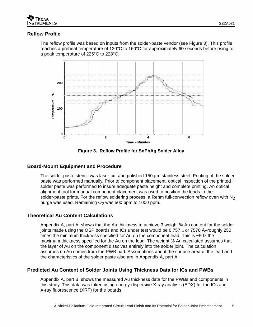
Reflow Profile
The reflow profile was based on inputs from the solder-paste vendor (see Figure 3). This profilereaches a preheat temperature of 120°C to 160°C for approximately 60 seconds before rising toa peak temperature of 225°C to 228°C.
200
0
100
02 4 6
Time – Minutes
Tem
per
atu
re –
C°
Figure 3. Reflow Profile for SnPbAg Solder Alloy
Board-Mount Equipment and Procedure
The solder paste stencil was laser-cut and polished 150-�m stainless steel. Printing of the solderpaste was performed manually. Prior to component placement, optical inspection of the printedsolder paste was performed to insure adequate paste height and complete printing. An opticalalignment tool for manual component placement was used to position the leads to thesolder-paste prints. For the reflow soldering process, a Rehm full-convection reflow oven with N2purge was used. Remaining O2 was 500 ppm to 1000 ppm.
Theoretical Au Content Calculations
Appendix A, part A, shows that the Au thickness to achieve 3 weight % Au content for the solderjoints made using the OSP boards and ICs under test would be 0.757 � or 7570 Å–roughly 250times the minimum thickness specified for Au on the component lead. This is ~50× themaximum thickness specified for the Au on the lead. The weight % Au calculated assumes thatthe layer of Au on the component dissolves entirely into the solder joint. The calculationassumes no Au comes from the PWB pad. Assumptions about the surface area of the lead andthe characteristics of the solder paste also are in Appendix A, part A.
Predicted Au Content of Solder Joints Using Thickness Data for ICs and PWBs
Appendix A, part B, shows the measured Au thickness data for the PWBs and components inthis study. This data was taken using energy-dispersive X-ray analysis (EDX) for the ICs andX-ray fluorescence (XRF) for the boards.
SZZA031
6 A Nickel-Palladium-Gold Integrated Circuit Lead Finish and Its Potential for Solder-Joint Embrittlement
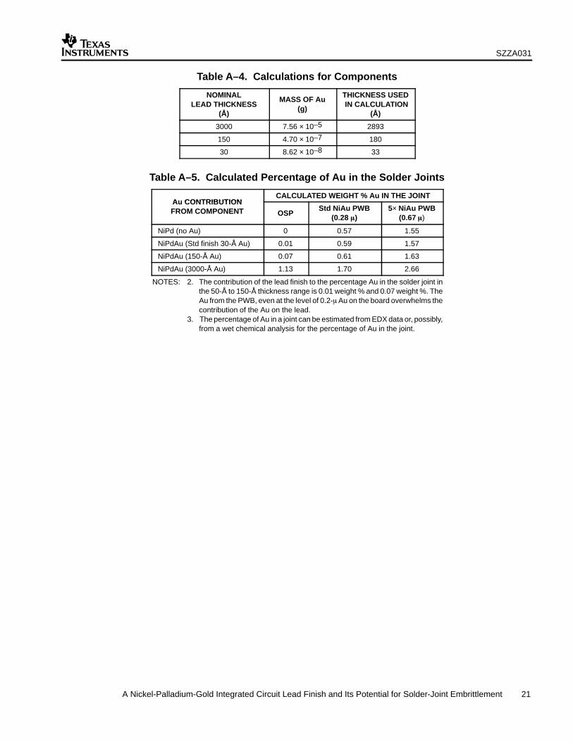
Appendix A, part C, shows the calculations for Au content in the solder joints for theembrittlement matrix in this study. The key conclusions about weight % Au in the joints areshown in Table 2. The simplistic approach taken for these calculations was that the Au layerdissolved completely and uniformly into the solder joint. The Au thickness was taken as theaverage. The other assumptions are noted in Appendix A.
Table 2. Calculated Weight % Au in the Solder Joints for the Test Matrix
Au CONTRIBUTIONFROM COMPONENT WEIGHT % Au IN THE JOINT (CALCULATED)
OSP Std NiAu PWB 5× NiAu PWB
NiPd (no Au) 0 0.57 1.55
NiPdAu (Std finish) 0.01 0.59 1.57
NiPdAu (5× Std finish) 0.07 0.61 1.63
NiPdAu (100× Std finish) 1.13 1.70 2.66
The calculated contribution of the component lead finish to the percentage Au in the solder jointin the standard and 5× NiPdAu thickness range is 0.01 weight % Au to 0.07 weight % Au. TheAu from the PWB, even at the standard level of Au on the board, overwhelms the contribution ofAu on the lead to the weight % Au in the joint. The Au flash on component leads poses anegligible risk of contributing to Au embrittlement of the solder joints made with suchcomponents.
Performance Measures and Results
Visual Appearance
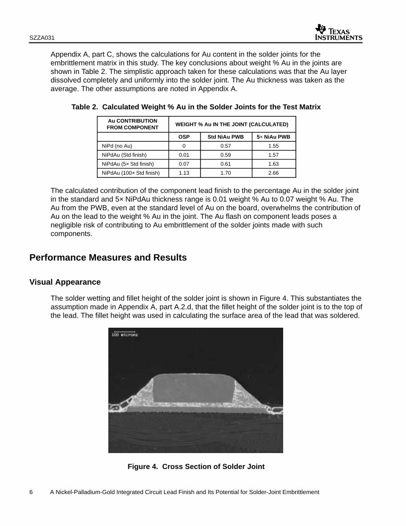
The solder wetting and fillet height of the solder joint is shown in Figure 4. This substantiates theassumption made in Appendix A, part A.2.d, that the fillet height of the solder joint is to the top ofthe lead. The fillet height was used in calculating the surface area of the lead that was soldered.
Figure 4. Cross Section of Solder Joint
SZZA031
7 A Nickel-Palladium-Gold Integrated Circuit Lead Finish and Its Potential for Solder-Joint Embrittlement
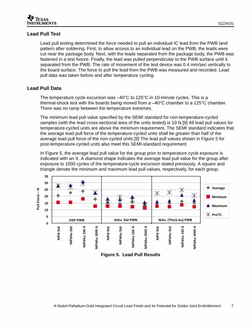
Lead Pull Test
Lead pull testing determined the force needed to pull an individual IC lead from the PWB landpattern after soldering. First, to allow access to an individual lead on the PWB, the leads werecut near the package body. Next, with the leads separated from the package body, the PWB wasfastened in a test fixture. Finally, the lead was pulled perpendicular to the PWB surface until itseparated from the PWB. The rate of movement of the test device was 0.4 mm/sec vertically tothe board surface. The force to pull the lead from the PWB was measured and recorded. Leadpull data was taken before and after temperature cycling.
Lead Pull Data
The temperature cycle excursion was –40°C to 125°C in 10-minute cycles. This is athermal-shock test with the boards being moved from a –40°C chamber to a 125°C chamber.There was no ramp between the temperature extremes.
The minimum lead pull value specified by the SEMI standard for non-temperature-cycledsamples (with the lead cross-sectional area of the units tested) is 10 N.[9] All lead pull values fortemperature-cycled units are above the minimum requirement. The SEMI standard indicates thatthe average lead pull force of the temperature-cycled units shall be greater than half of theaverage lead pull force of the non-cycled units.[9] The lead pull values shown in Figure 5 forpost-temperature-cycled units also meet this SEMI-standard requirement.
In Figure 5, the average lead pull value for the group prior to temperature cycle exposure isindicated with an X. A diamond shape indicates the average lead pull value for the group afterexposure to 1000 cycles of the temperature-cycle excursion stated previously. A square andtriangle denote the minimum and maximum lead pull values, respectively, for each group.
0
5
10
15
20
25
30
35
NiP
d S
td
NiP
dA
u S
td
NiP
dA
u 1
50
NiP
dA
u 3
000
NiP
d S
td
NiP
dA
u S
td
NiP
dA
u 1
50
NiP
dA
u 3
000
NiP
d S
td
NiP
dA
u S
td
NiP
dA
u 1
50
NiP
dA
u 3
000
Pu
ll F
orc
e –
N Average
Minimum
Maximum
PreTC
OSP PWB NiAu Std PWB NiAu (Thick Au) PWB
AAAA AA
Figure 5. Lead Pull Results
SZZA031
8 A Nickel-Palladium-Gold Integrated Circuit Lead Finish and Its Potential for Solder-Joint Embrittlement
Observations From Lead Pull Results
For the combinations of OSP PWB pad finish and NiPdAu, component finishes with standard Authickness and 5× Au show slightly higher lead pull values compared to NiPd component finish(no Au). Lead pull values for NiPdAu finish with 100× Au are slightly less compared to the otherthree samples. For the standard NiAu pad finish, lead pull values with NiPd, standard NiPdAu,and 5× Au are all essentially equivalent. The NiPdAu component finish with 100× Au is onlyslightly lower than the other three. These results are about 25% lower than the OSP results. Forthe 5× Std NiAu PWB finish, the four lead pull values (post-temperature cycle) are essentiallythe same as those of the standard NiAu-pad-finish board.
The most significant drop between pre-temperature-cycled and post-temperature-cycled leadpull averages is noted for all four groups in the 5× NiAu PWB finish. The eight samples mountedon NiAu PWB finish (both standard PWB Au thickness and 5× PWB Au thickness) appear to be,as a group, lower than the four samples mounted on an OSP pad finish. The difference is about25%.
Statistical Analysis of Lead Pull Data
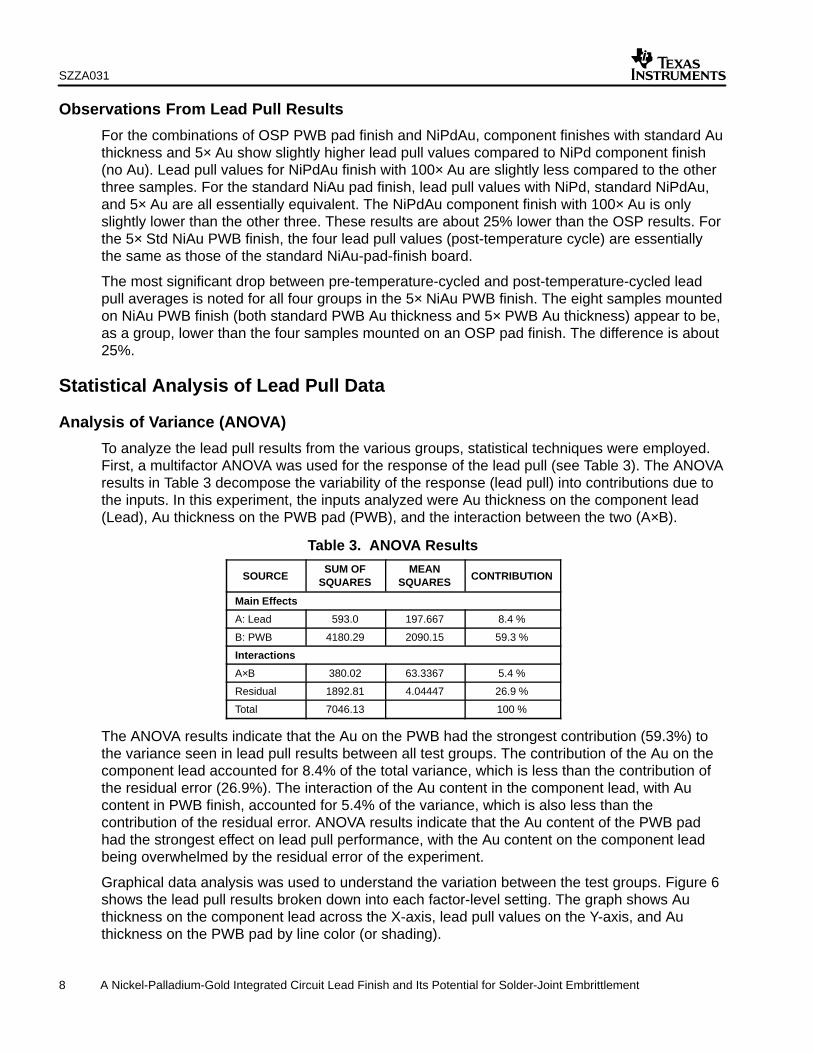
Analysis of Variance (ANOVA)
To analyze the lead pull results from the various groups, statistical techniques were employed.First, a multifactor ANOVA was used for the response of the lead pull (see Table 3). The ANOVAresults in Table 3 decompose the variability of the response (lead pull) into contributions due tothe inputs. In this experiment, the inputs analyzed were Au thickness on the component lead(Lead), Au thickness on the PWB pad (PWB), and the interaction between the two (A×B).
Table 3. ANOVA Results
SOURCESUM OF
SQUARESMEAN
SQUARES CONTRIBUTION
Main Effects
A: Lead 593.0 197.667 8.4 %
B: PWB 4180.29 2090.15 59.3 %
Interactions
A×B 380.02 63.3367 5.4 %
Residual 1892.81 4.04447 26.9 %
Total 7046.13 100 %
The ANOVA results indicate that the Au on the PWB had the strongest contribution (59.3%) tothe variance seen in lead pull results between all test groups. The contribution of the Au on thecomponent lead accounted for 8.4% of the total variance, which is less than the contribution ofthe residual error (26.9%). The interaction of the Au content in the component lead, with Aucontent in PWB finish, accounted for 5.4% of the variance, which is also less than thecontribution of the residual error. ANOVA results indicate that the Au content of the PWB padhad the strongest effect on lead pull performance, with the Au content on the component leadbeing overwhelmed by the residual error of the experiment.
Graphical data analysis was used to understand the variation between the test groups. Figure 6shows the lead pull results broken down into each factor-level setting. The graph shows Authickness on the component lead across the X-axis, lead pull values on the Y-axis, and Authickness on the PWB pad by line color (or shading).
SZZA031
9 A Nickel-Palladium-Gold Integrated Circuit Lead Finish and Its Potential for Solder-Joint Embrittlement
0
5
10
15
20
25
0 30 150 3000
OSP
NiAu (Std)
NiAu (Thick Au)
Au Thickness on Component Lead – Å
Pu
ll F
orc
e –
N
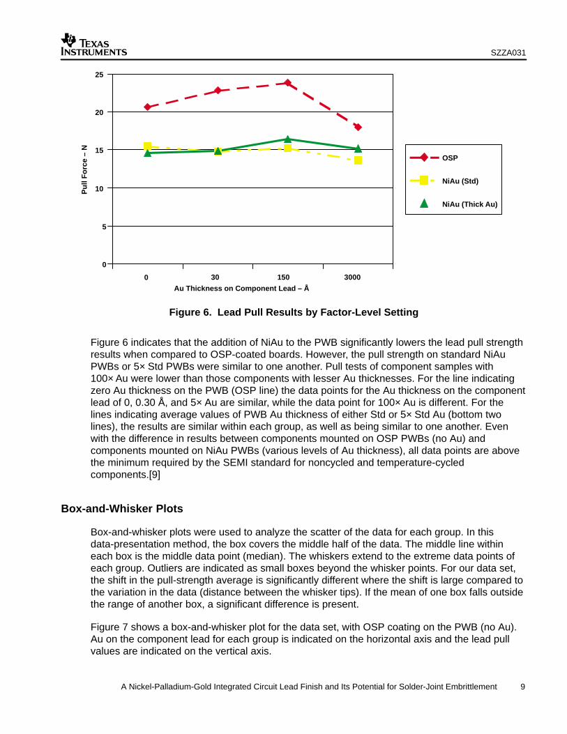
Figure 6. Lead Pull Results by Factor-Level Setting
Figure 6 indicates that the addition of NiAu to the PWB significantly lowers the lead pull strengthresults when compared to OSP-coated boards. However, the pull strength on standard NiAuPWBs or 5× Std PWBs were similar to one another. Pull tests of component samples with100× Au were lower than those components with lesser Au thicknesses. For the line indicatingzero Au thickness on the PWB (OSP line) the data points for the Au thickness on the componentlead of 0, 0.30 Å, and 5× Au are similar, while the data point for 100× Au is different. For thelines indicating average values of PWB Au thickness of either Std or 5× Std Au (bottom twolines), the results are similar within each group, as well as being similar to one another. Evenwith the difference in results between components mounted on OSP PWBs (no Au) andcomponents mounted on NiAu PWBs (various levels of Au thickness), all data points are abovethe minimum required by the SEMI standard for noncycled and temperature-cycledcomponents.[9]
Box-and-Whisker Plots
Box-and-whisker plots were used to analyze the scatter of the data for each group. In thisdata-presentation method, the box covers the middle half of the data. The middle line withineach box is the middle data point (median). The whiskers extend to the extreme data points ofeach group. Outliers are indicated as small boxes beyond the whisker points. For our data set,the shift in the pull-strength average is significantly different where the shift is large compared tothe variation in the data (distance between the whisker tips). If the mean of one box falls outsidethe range of another box, a significant difference is present.
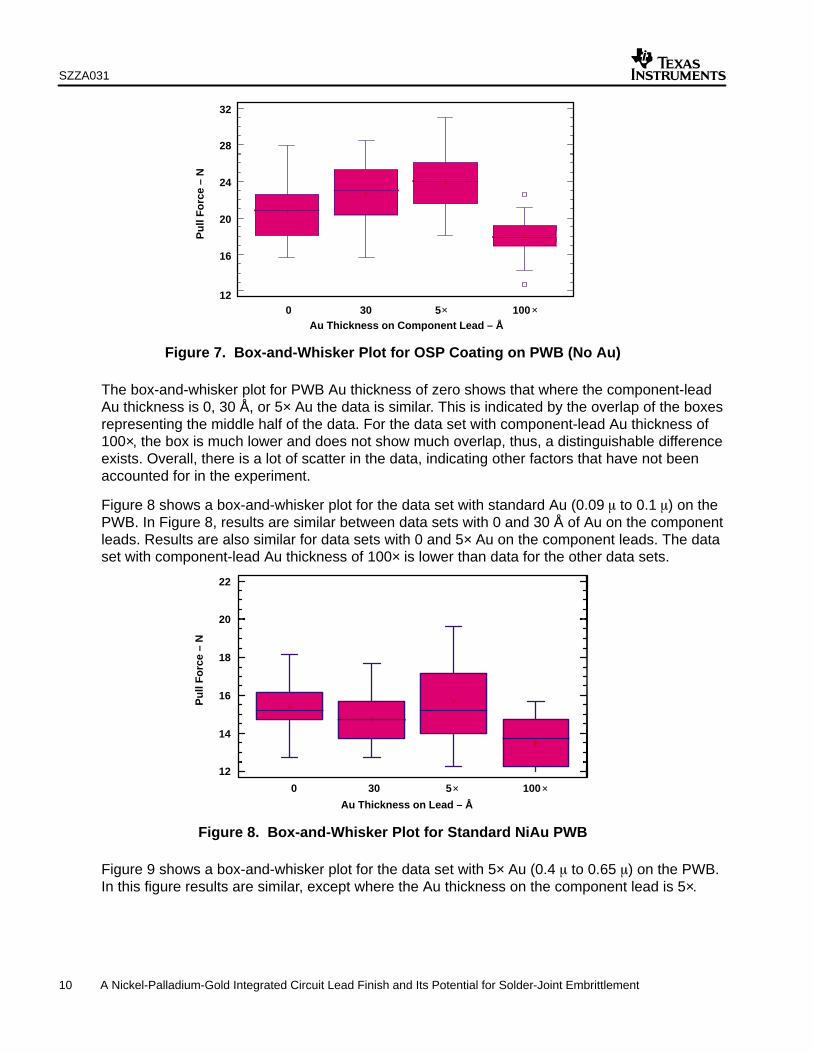
Figure 7 shows a box-and-whisker plot for the data set, with OSP coating on the PWB (no Au).Au on the component lead for each group is indicated on the horizontal axis and the lead pullvalues are indicated on the vertical axis.
SZZA031
10 A Nickel-Palladium-Gold Integrated Circuit Lead Finish and Its Potential for Solder-Joint Embrittlement
Au Thickness on Component Lead – Å
Pu
ll F
orc
e –
N
0 30 5 10012
16
20
24
28
32
× ×
Figure 7. Box-and-Whisker Plot for OSP Coating on PWB (No Au)
The box-and-whisker plot for PWB Au thickness of zero shows that where the component-leadAu thickness is 0, 30 Å, or 5× Au the data is similar. This is indicated by the overlap of the boxesrepresenting the middle half of the data. For the data set with component-lead Au thickness of100×, the box is much lower and does not show much overlap, thus, a distinguishable differenceexists. Overall, there is a lot of scatter in the data, indicating other factors that have not beenaccounted for in the experiment.
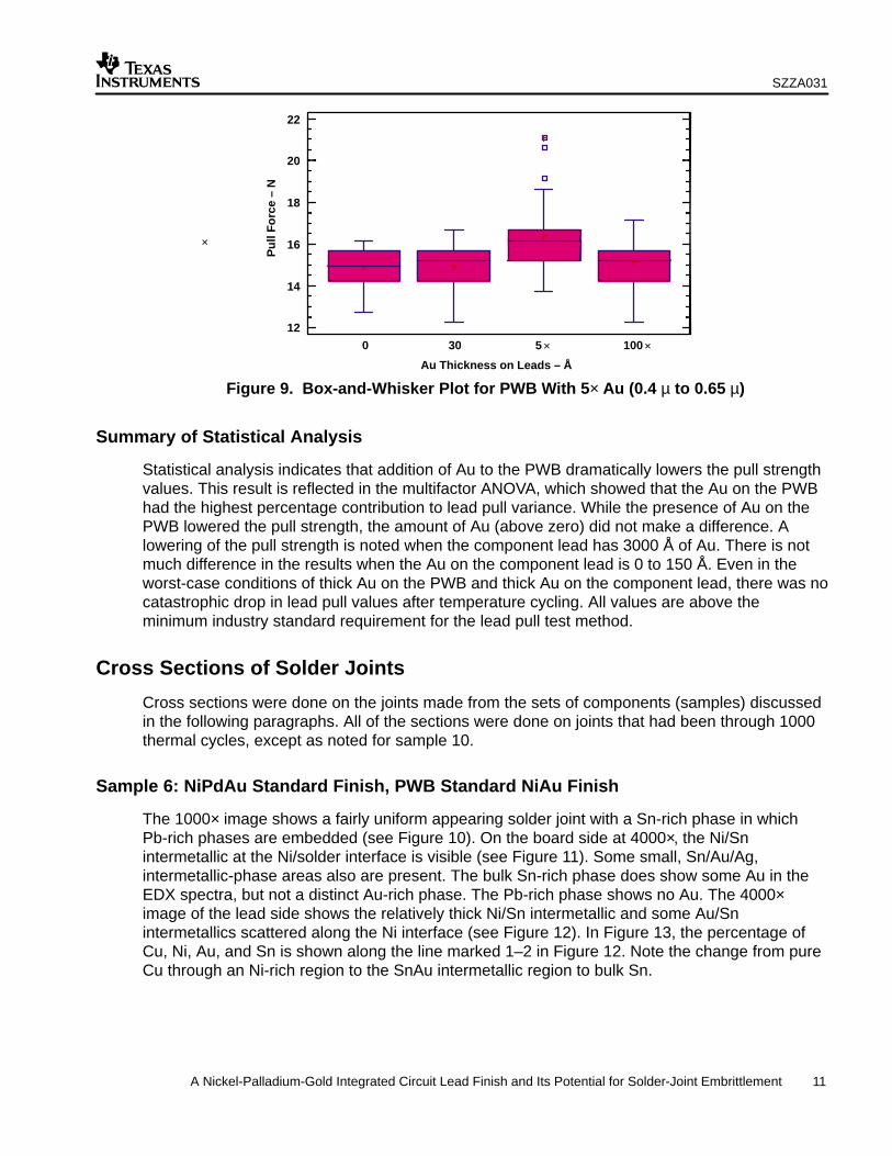
Figure 8 shows a box-and-whisker plot for the data set with standard Au (0.09 � to 0.1 �) on thePWB. In Figure 8, results are similar between data sets with 0 and 30 Å of Au on the componentleads. Results are also similar for data sets with 0 and 5× Au on the component leads. The dataset with component-lead Au thickness of 100× is lower than data for the other data sets.
Pu
ll F
orc
e –
N
0 30 5 100
12
14
16
18
20
22
Au Thickness on Lead – Å
× ×
Figure 8. Box-and-Whisker Plot for Standard NiAu PWB
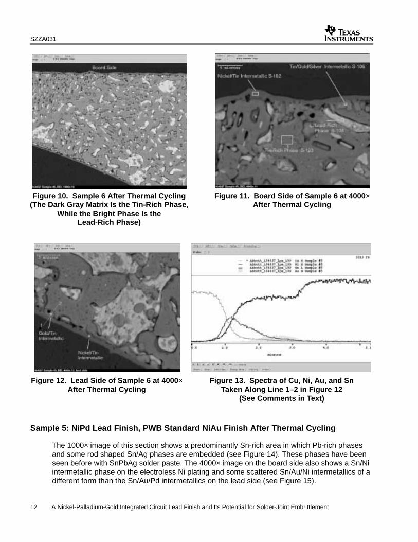
Figure 9 shows a box-and-whisker plot for the data set with 5× Au (0.4 � to 0.65 �) on the PWB.In this figure results are similar, except where the Au thickness on the component lead is 5×.
SZZA031
11 A Nickel-Palladium-Gold Integrated Circuit Lead Finish and Its Potential for Solder-Joint Embrittlement
Pu
ll F
orc
e –
N
0 30 5 100
12
14
16
18
20
22
Au Thickness on Leads – Å
×
× ×
Figure 9. Box-and-Whisker Plot for PWB With 5× Au (0.4 µ to 0.65 µ)
Summary of Statistical Analysis
Statistical analysis indicates that addition of Au to the PWB dramatically lowers the pull strengthvalues. This result is reflected in the multifactor ANOVA, which showed that the Au on the PWBhad the highest percentage contribution to lead pull variance. While the presence of Au on thePWB lowered the pull strength, the amount of Au (above zero) did not make a difference. Alowering of the pull strength is noted when the component lead has 3000 Å of Au. There is notmuch difference in the results when the Au on the component lead is 0 to 150 Å. Even in theworst-case conditions of thick Au on the PWB and thick Au on the component lead, there was nocatastrophic drop in lead pull values after temperature cycling. All values are above theminimum industry standard requirement for the lead pull test method.
Cross Sections of Solder Joints
Cross sections were done on the joints made from the sets of components (samples) discussedin the following paragraphs. All of the sections were done on joints that had been through 1000thermal cycles, except as noted for sample 10.
Sample 6: NiPdAu Standard Finish, PWB Standard NiAu Finish
The 1000× image shows a fairly uniform appearing solder joint with a Sn-rich phase in whichPb-rich phases are embedded (see Figure 10). On the board side at 4000×, the Ni/Snintermetallic at the Ni/solder interface is visible (see Figure 11). Some small, Sn/Au/Ag,intermetallic-phase areas also are present. The bulk Sn-rich phase does show some Au in theEDX spectra, but not a distinct Au-rich phase. The Pb-rich phase shows no Au. The 4000×image of the lead side shows the relatively thick Ni/Sn intermetallic and some Au/Snintermetallics scattered along the Ni interface (see Figure 12). In Figure 13, the percentage ofCu, Ni, Au, and Sn is shown along the line marked 1–2 in Figure 12. Note the change from pureCu through an Ni-rich region to the SnAu intermetallic region to bulk Sn.
SZZA031
12 A Nickel-Palladium-Gold Integrated Circuit Lead Finish and Its Potential for Solder-Joint Embrittlement
Figure 10. Sample 6 After Thermal Cycling(The Dark Gray Matrix Is the Tin-Rich Phase,
While the Bright Phase Is theLead-Rich Phase)
Figure 11. Board Side of Sample 6 at 4000×After Thermal Cycling
Figure 12. Lead Side of Sample 6 at 4000×After Thermal Cycling
Figure 13. Spectra of Cu, Ni, Au, and SnTaken Along Line 1–2 in Figure 12
(See Comments in Text)
Sample 5: NiPd Lead Finish, PWB Standard NiAu Finish After Thermal Cycling
The 1000× image of this section shows a predominantly Sn-rich area in which Pb-rich phasesand some rod shaped Sn/Ag phases are embedded (see Figure 14). These phases have beenseen before with SnPbAg solder paste. The 4000× image on the board side also shows a Sn/Niintermetallic phase on the electroless Ni plating and some scattered Sn/Au/Ni intermetallics of adifferent form than the Sn/Au/Pd intermetallics on the lead side (see Figure 15).
SZZA031
13 A Nickel-Palladium-Gold Integrated Circuit Lead Finish and Its Potential for Solder-Joint Embrittlement
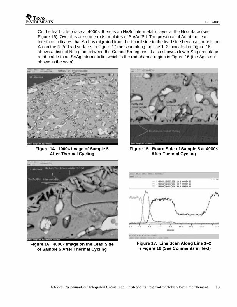
On the lead-side phase at 4000×, there is an Ni/Sn intermetallic layer at the Ni surface (seeFigure 16). Over this are some rods or plates of Sn/Au/Pd. The presence of Au at the leadinterface indicates that Au has migrated from the board side to the lead side because there is noAu on the NiPd lead surface. In Figure 17 the scan along the line 1–2 indicated in Figure 16,shows a distinct Ni region between the Cu and Sn regions. It also shows a lower Sn percentageattributable to an SnAg intermetallic, which is the rod-shaped region in Figure 16 (the Ag is notshown in the scan).
Figure 14. 1000× Image of Sample 5After Thermal Cycling
Figure 15. Board Side of Sample 5 at 4000×After Thermal Cycling
Figure 16. 4000× Image on the Lead Sideof Sample 5 After Thermal Cycling
Figure 17. Line Scan Along Line 1–2in Figure 16 (See Comments in Text)
SZZA031
14 A Nickel-Palladium-Gold Integrated Circuit Lead Finish and Its Potential for Solder-Joint Embrittlement
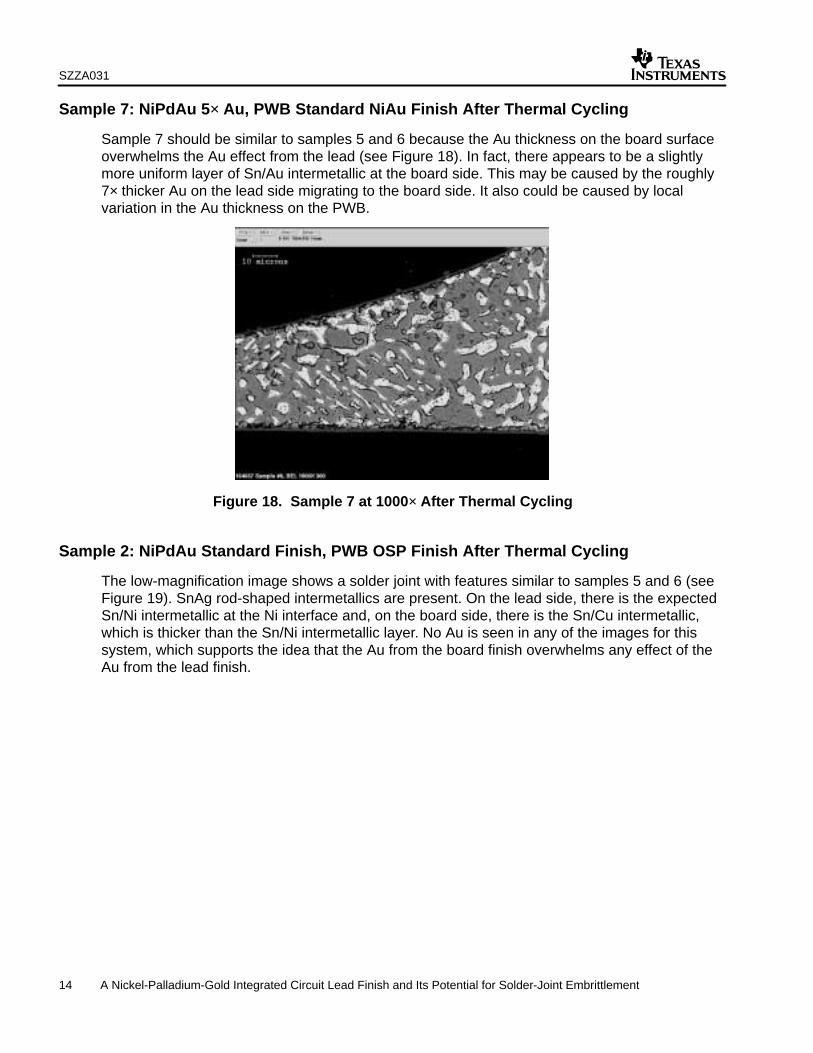
Sample 7: NiPdAu 5× Au, PWB Standard NiAu Finish After Thermal Cycling
Sample 7 should be similar to samples 5 and 6 because the Au thickness on the board surfaceoverwhelms the Au effect from the lead (see Figure 18). In fact, there appears to be a slightlymore uniform layer of Sn/Au intermetallic at the board side. This may be caused by the roughly7× thicker Au on the lead side migrating to the board side. It also could be caused by localvariation in the Au thickness on the PWB.
Figure 18. Sample 7 at 1000× After Thermal Cycling
Sample 2: NiPdAu Standard Finish, PWB OSP Finish After Thermal Cycling
The low-magnification image shows a solder joint with features similar to samples 5 and 6 (seeFigure 19). SnAg rod-shaped intermetallics are present. On the lead side, there is the expectedSn/Ni intermetallic at the Ni interface and, on the board side, there is the Sn/Cu intermetallic,which is thicker than the Sn/Ni intermetallic layer. No Au is seen in any of the images for thissystem, which supports the idea that the Au from the board finish overwhelms any effect of theAu from the lead finish.

SZZA031
15 A Nickel-Palladium-Gold Integrated Circuit Lead Finish and Its Potential for Solder-Joint Embrittlement
Figure 19. 1000× Image of Sample 2 After Thermal Cycling
Sample 10: NiPdAu Standard Finish, 5× NiAu PWB With No Thermal Cycling
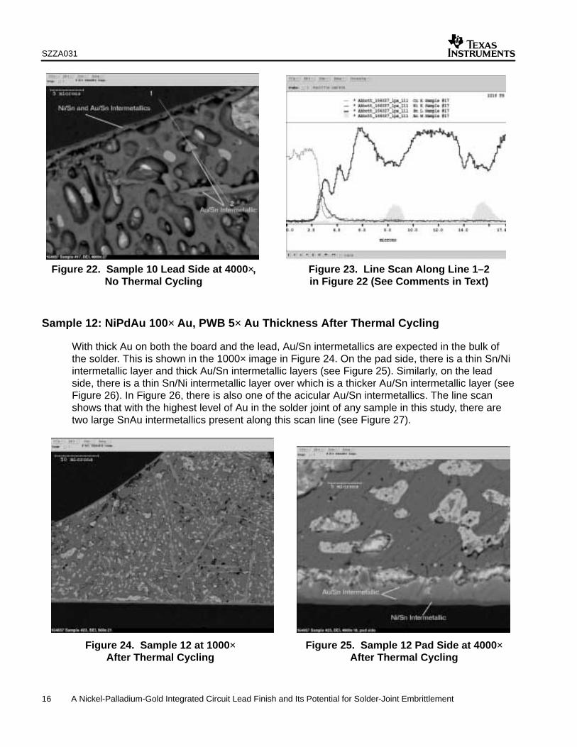
This sample was not thermal cycled. Figure 20 shows large numbers of Sn/Au acicularintermetallics dispersed in the bulk of the solder joint. The Sn/Ni intermetallics at both the board(see Figure 21) and lead (see Figure 22) surfaces are thinner than for the thermally cycledsamples, which is expected. On the lead side there are Sn/Au regions that are detached fromthe Sn/Ni and Sn/Au intermetallics on the surface. The Sn/Au intermetallic layer appears tooverlie the Sn/Ni layer that is on the Ni layer. The line scan, clearly shows that the SnAuintermetallics at that location form because of the high Au content of the PWB and theseintermetallics are showing up at the lead side of the joint (see Figure 23). This shows themobility of Au in molten solder.
Figure 20. 1000× Image of Sample 10,No Thermal Cycling
Figure 21. Sample 10 at 4000× Board Side,No Thermal Cycling
SZZA031
16 A Nickel-Palladium-Gold Integrated Circuit Lead Finish and Its Potential for Solder-Joint Embrittlement
Figure 22. Sample 10 Lead Side at 4000×,No Thermal Cycling
Figure 23. Line Scan Along Line 1–2in Figure 22 (See Comments in Text)
Sample 12: NiPdAu 100× Au, PWB 5× Au Thickness After Thermal Cycling
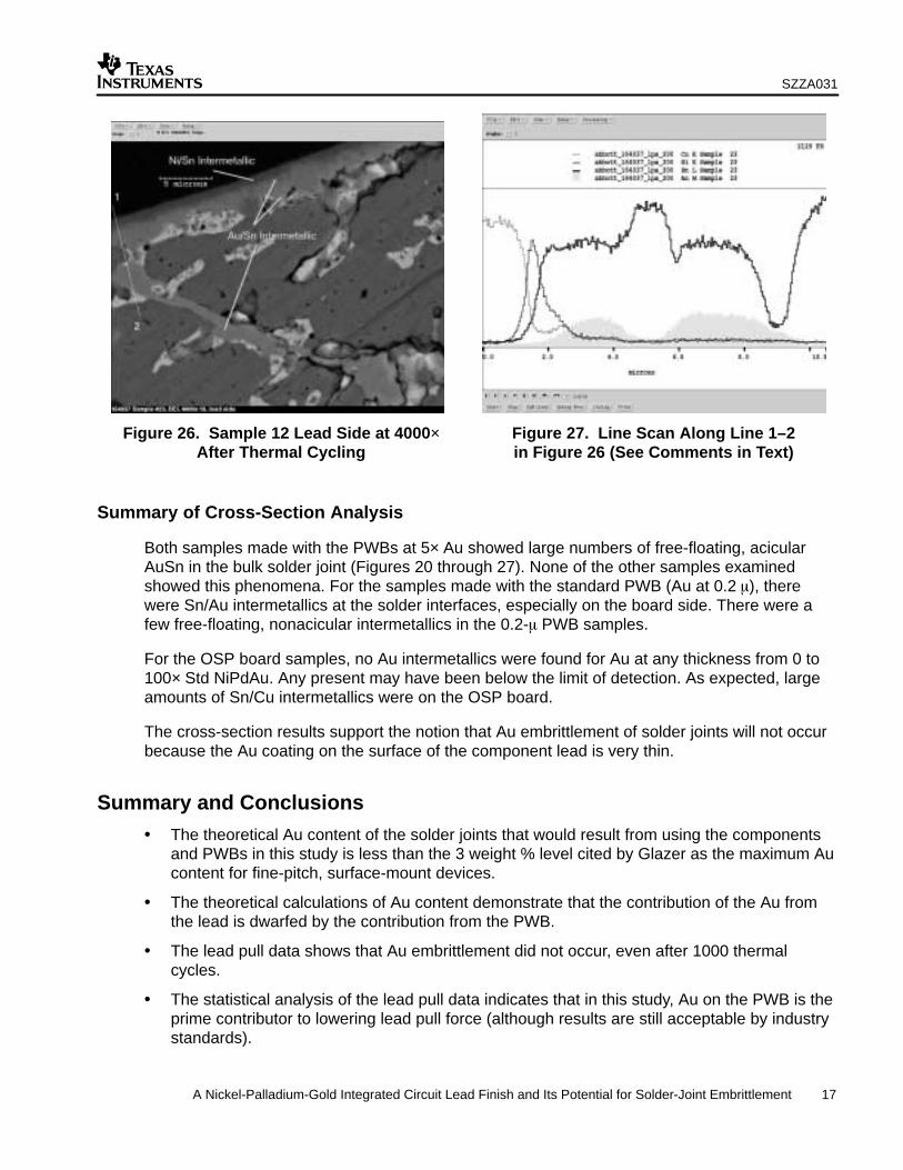
With thick Au on both the board and the lead, Au/Sn intermetallics are expected in the bulk ofthe solder. This is shown in the 1000× image in Figure 24. On the pad side, there is a thin Sn/Niintermetallic layer and thick Au/Sn intermetallic layers (see Figure 25). Similarly, on the leadside, there is a thin Sn/Ni intermetallic layer over which is a thicker Au/Sn intermetallic layer (seeFigure 26). In Figure 26, there is also one of the acicular Au/Sn intermetallics. The line scanshows that with the highest level of Au in the solder joint of any sample in this study, there aretwo large SnAu intermetallics present along this scan line (see Figure 27).
Figure 24. Sample 12 at 1000×After Thermal Cycling
Figure 25. Sample 12 Pad Side at 4000×After Thermal Cycling
SZZA031
17 A Nickel-Palladium-Gold Integrated Circuit Lead Finish and Its Potential for Solder-Joint Embrittlement
Figure 26. Sample 12 Lead Side at 4000×After Thermal Cycling
Figure 27. Line Scan Along Line 1–2in Figure 26 (See Comments in Text)
Summary of Cross-Section Analysis
Both samples made with the PWBs at 5× Au showed large numbers of free-floating, acicularAuSn in the bulk solder joint (Figures 20 through 27). None of the other samples examinedshowed this phenomena. For the samples made with the standard PWB (Au at 0.2 �), therewere Sn/Au intermetallics at the solder interfaces, especially on the board side. There were afew free-floating, nonacicular intermetallics in the 0.2-� PWB samples.
For the OSP board samples, no Au intermetallics were found for Au at any thickness from 0 to100× Std NiPdAu. Any present may have been below the limit of detection. As expected, largeamounts of Sn/Cu intermetallics were on the OSP board.
The cross-section results support the notion that Au embrittlement of solder joints will not occurbecause the Au coating on the surface of the component lead is very thin.
Summary and Conclusions• The theoretical Au content of the solder joints that would result from using the components
and PWBs in this study is less than the 3 weight % level cited by Glazer as the maximum Aucontent for fine-pitch, surface-mount devices.
• The theoretical calculations of Au content demonstrate that the contribution of the Au fromthe lead is dwarfed by the contribution from the PWB.
• The lead pull data shows that Au embrittlement did not occur, even after 1000 thermalcycles.
• The statistical analysis of the lead pull data indicates that in this study, Au on the PWB is theprime contributor to lowering lead pull force (although results are still acceptable by industrystandards).
SZZA031
18 A Nickel-Palladium-Gold Integrated Circuit Lead Finish and Its Potential for Solder-Joint Embrittlement
• The metallographic data shows that:
– The solder joint is made to the Ni surface of the component lead.
– There is no Cu migration through the Ni barrier layer of the lead.
– In a system with no Au on the PWB and with a standard Au thickness on the lead, thereis no Au detectable in the bulk of the solder joint.
– The Au from the PWB can migrate across the solder joint and appear at the lead/solderinterface in the case of the NiPd-finished lead.
– At very high Au thicknesses on PWB and leads but give Au concentrations of less than 3weight %, acicular SnAu intermetallics do form. These do not appear to be sufficient toaffect pull strength.
• The risk of Au embrittlement caused by TI’s NiPdAu component lead finish is essentially nil.
Acknowledgments
The authors wish to recognize the following individuals for their professional assistance:
– Kay Haulick and Martin Pauli for their board mounts, visual documentation, and lead pulltesting
– Dr. Al Hopkins of the Texas Instruments Attleboro S&C Group for the cross sections andSEM/EDX work
– Bill Russell of Raytheon Technologies for support with statistical analysis of lead pull data
The authors wish to recognize Multicore for supplying the SnPbAg solder paste used in thisstudy.
References1. D. C. Abbott, R. M. Brook, N. McLellan, and J. S. Wiley, IEEE Trans. CHMT, 14:567 (1991).
2. A. Murata and D. C. Abbott, Technical Proceedings, Semicon Japan, p. 415 (1990).
3. J. Glazer, P. A. Kramer, and J. W. Morris, “Effect of Au on the Reliability of Fine Pitch SurfaceMount Solder Joints”, Proceedings of the Technical Program, Surface Mount InternationalConference & Exhibition, August 1991, pp. 629–639.
4. E. E. de Kluizenaar, Soldering and Surface Mount Technology, No. 4, February 1990. pp. 27–38.
5. M. F. Bester, Proceedings of Internepcon, 1968, pp. 211–231.
6. F. G. Foster, ASTM STP 319, 1963, p. 13.
7. R. Druckett and M. L. Ackroyd, Electropl. Met. Fin., Vol. 29, 1976, pp. 13–20.
8. A. Zribi et al., IEEE Transactions on Components and Packaging Technologies, Vol. 23, No. 2,June 2000.
9. IPC-A-610C, Acceptability of Electronic Assemblies, January 2000.
SZZA031
19 A Nickel-Palladium-Gold Integrated Circuit Lead Finish and Its Potential for Solder-Joint Embrittlement
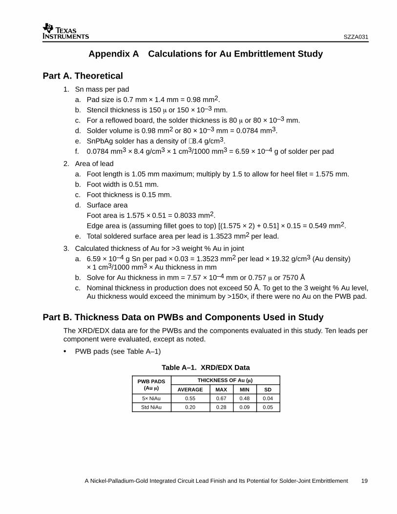
Appendix A Calculations for Au Embrittlement Study
Part A. Theoretical1. Sn mass per pad
a. Pad size is 0.7 mm × 1.4 mm = 0.98 mm2.
b. Stencil thickness is 150 � or 150 × 10–3 mm.
c. For a reflowed board, the solder thickness is 80 � or 80 × 10–3 mm.
d. Solder volume is 0.98 mm2 or 80 × 10–3 mm = 0.0784 mm3.
e. SnPbAg solder has a density of ∼ 8.4 g/cm3.
f. 0.0784 mm3 × 8.4 g/cm3 × 1 cm3/1000 mm3 = 6.59 × 10⁻⁴ g of solder per pad
2. Area of lead
a. Foot length is 1.05 mm maximum; multiply by 1.5 to allow for heel filet = 1.575 mm.
b. Foot width is 0.51 mm.
c. Foot thickness is 0.15 mm.
d. Surface area
Foot area is 1.575 × 0.51 = 0.8033 mm2.
Edge area is (assuming fillet goes to top) [(1.575 × 2) + 0.51] × 0.15 = 0.549 mm2.
e. Total soldered surface area per lead is 1.3523 mm2 per lead.
3. Calculated thickness of Au for >3 weight % Au in joint
a. 6.59 × 10⁻⁴ g Sn per pad × 0.03 = 1.3523 mm2 per lead × 19.32 g/cm3 (Au density) × 1 cm3/1000 mm3 × Au thickness in mm
b. Solve for Au thickness in mm = 7.57 × 10⁻⁴ mm or 0.757 � or 7570 Å
c. Nominal thickness in production does not exceed 50 Å. To get to the 3 weight % Au level,Au thickness would exceed the minimum by >150×, if there were no Au on the PWB pad.
Part B. Thickness Data on PWBs and Components Used in StudyThe XRD/EDX data are for the PWBs and the components evaluated in this study. Ten leads percomponent were evaluated, except as noted.
• PWB pads (see Table A–1)
Table A–1. XRD/EDX Data
PWB PADS THICKNESS OF Au (�)(Au �) AVERAGE MAX MIN SD
5× NiAu 0.55 0.67 0.48 0.04
Std NiAu 0.20 0.28 0.09 0.05
SZZA031
20 A Nickel-Palladium-Gold Integrated Circuit Lead Finish and Its Potential for Solder-Joint Embrittlement
• Devices (see Table A–2)
Table A–2. XRF/EDX Data
COMPONENTSTHICKNESS OF Au (Å)
COMPONENTSAVERAGE MAX MIN SD
3000 Å 2893 4325 2225 722
150 Å 180 250 125 42
×1835† 33 37 30 3
† Sub-50-Å data obtained by EDXNOTE 1: 1 � = 10,000 Å = 10 × 10–3 mm
Part C. Calculations of Au Concentration in Parts Used in the StudyThis part gives calculations of the percentage of Au in the joints we made, accounting for the Auon the PWB pads. The averages of measured Au values are used in the calculations.
4. Boards (see Table A–3)
a. Pad size is 0.7 mm × 1.4 mm = 0.98 mm2.
b. Au thickness on board 38a is 0.55 � or 5.5 × 10⁻⁴ mm.
c. Au thickness on board 39a is 0.20 � or 2.0 × 10⁻⁴ mm.
d. Mass of Au on 38a is
0.98 mm2 × 5.5 × 10–4 mm × 1 cm3/1000 mm3 × 19.32 g/cm3 = 1.04 × 10⁻⁵ g Au/pad.
e. Mass of Au on 39a is
0.98 mm2 × 2.0 × 10–4 mm × 1 cm3/1000 mm3 × 19.32 g/cm3 = 3.79 × 10⁻⁶ g Au/pad.
5. Components (see Table A–4)
a. Total soldered surface area per lead is 1.3523 mm2.
b. For the nominal 3000-Å leads:
1.3523 mm2 × 2.893 × 10–4 mm × 1 cm3/1000 mm3 × 19.32 = 7.56 × 10⁻⁶ g Au/lead
c. For the nominal 150-Å leads:
1.3523 mm2 × 1.80 × 10–5 mm × 1 cm3/1000 mm3 × 19.32 = 4.70 ×10⁻⁷ g Au/lead
d. For nominal 30-Å leads:
1.3523 mm2 × 3.3 × 10–6 mm × 1 cm3/1000 mm3 × 19.32 = 8.62 × 10⁻⁸ g Au/lead
6. Percentage of Au in solder joints (general formula) (see Table A–5)
a. Percentage of Au = [(mass Au on lead + mass Au on pad)/(mass of Sn + mass Au onlead + mass Au on pad)] × 100
b. Mass of solder joint = 6.59 × 10⁻⁴ g
Table A–3. Calculations for Boards
FORBOARDS
MASS OF Au(g)
THICKNESS USEDIN CALCULATION
(�)
38a 1.04 × 10⁻⁵ 0.55
39a 3.79 × 10⁻⁶ 0.20
SZZA031
21 A Nickel-Palladium-Gold Integrated Circuit Lead Finish and Its Potential for Solder-Joint Embrittlement
Table A–4. Calculations for Components
NOMINALLEAD THICKNESS
(Å)
MASS OF Au(g)
THICKNESS USED IN CALCULATION
(Å)
3000 7.56 × 10⁻⁵ 2893
150 4.70 × 10⁻⁷ 180
30 8.62 × 10⁻⁸ 33
Table A–5. Calculated Percentage of Au in the Solder Joints
A CONTRIBUTIONCALCULATED WEIGHT % Au IN THE JOINT
Au CONTRIBUTIONFROM COMPONENT OSP
Std NiAu PWB(0.28 �)
5× NiAu PWB(0.67 �)
NiPd (no Au) 0 0.57 1.55
NiPdAu (Std finish 30-Å Au) 0.01 0.59 1.57
NiPdAu (150-Å Au) 0.07 0.61 1.63
NiPdAu (3000-Å Au) 1.13 1.70 2.66
NOTES: 2. The contribution of the lead finish to the percentage Au in the solder joint inthe 50-Å to 150-Å thickness range is 0.01 weight % and 0.07 weight %. TheAu from the PWB, even at the level of 0.2-� Au on the board overwhelms thecontribution of the Au on the lead.
3. The percentage of Au in a joint can be estimated from EDX data or, possibly,from a wet chemical analysis for the percentage of Au in the joint.
IMPORTANT NOTICE
Texas Instruments Incorporated and its subsidiaries (TI) reserve the right to make corrections, modifications,enhancements, improvements, and other changes to its products and services at any time and to discontinueany product or service without notice. Customers should obtain the latest relevant information before placingorders and should verify that such information is current and complete. All products are sold subject to TI’s termsand conditions of sale supplied at the time of order acknowledgment.
TI warrants performance of its hardware products to the specifications applicable at the time of sale inaccordance with TI’s standard warranty. Testing and other quality control techniques are used to the extent TIdeems necessary to support this warranty. Except where mandated by government requirements, testing of allparameters of each product is not necessarily performed.
TI assumes no liability for applications assistance or customer product design. Customers are responsible fortheir products and applications using TI components. To minimize the risks associated with customer productsand applications, customers should provide adequate design and operating safeguards.
TI does not warrant or represent that any license, either express or implied, is granted under any TI patent right,copyright, mask work right, or other TI intellectual property right relating to any combination, machine, or processin which TI products or services are used. Information published by TI regarding third–party products or servicesdoes not constitute a license from TI to use such products or services or a warranty or endorsement thereof.Use of such information may require a license from a third party under the patents or other intellectual propertyof the third party, or a license from TI under the patents or other intellectual property of TI.
Reproduction of information in TI data books or data sheets is permissible only if reproduction is withoutalteration and is accompanied by all associated warranties, conditions, limitations, and notices. Reproductionof this information with alteration is an unfair and deceptive business practice. TI is not responsible or liable forsuch altered documentation.
Resale of TI products or services with statements different from or beyond the parameters stated by TI for thatproduct or service voids all express and any implied warranties for the associated TI product or service andis an unfair and deceptive business practice. TI is not responsible or liable for any such statements.
Mailing Address:
Texas InstrumentsPost Office Box 655303Dallas, Texas 75265
Copyright 2001, Texas Instruments Incorporated