Embed Size (px)
Citation preview
A SELF-CALIBRATING LOW POWER 16-BIT 500KSPS CHARGE-
REDISTRIBUTION SAR ANALOG-TO-DIGITAL CONVERTER
By
PRASANNA UPADHYAYA
A thesis submitted in partial fulfillment of
the requirements for the degree of
MASTER OF SCIENCE IN ELECTRICAL ENGINEERING
WASHINGTON STATE UNIVERSITY
School of Electrical Engineering and Computer Science
AUGUST 2008

ii
To the Faculty of Washington State University:
The members of the Committee appointed to examine the thesis of
PRASANNA UPADHYAYA find it satisfactory and recommend that it be
accepted.
___________________________________
Chair
___________________________________
___________________________________

iii
ACKNOWLEDGEMENT
Throughout my stay at Washington State University, I have worked with
numerous great personalities, who helped me focus on the ultimate goal of completing
research and thesis work. Their contribution in assorted ways to the research and
finishing of this thesis deserves special acknowledgment. Therefore, I want to take this
opportunity to pay my homage to them. I am grateful to David Rector, associate professor
at Department of Veterinary and Comparative Anatomy, Pharmacology and Physiology
(VCAAP), for funding the research work required to complete this thesis.
I am appreciative of my advisor, Dr. George S. La Rue, for his invaluable support
and guidance towards finishing this work. I would also like to thank my colleagues Wei
Zheng, Haidong Guo, Erik Wemlinger, Saurabh Mandhanya, and Ding Ma for creating
the productive and fun-filled work atmosphere. Especially, I want to thank Kun Yang and
Hari Krishnan Krishamurthy for their assistance on various portions of this work. In
addition, I am grateful for jovial conversations with Pinping Sun, Jaeyoung Jung, and
greatest of them all Bill Hamon, the great entertainer. Furthermore, enlightening and
sometimes non-technical discussion with Dirk Robinson and Prof. La Rue made research
work less troubling and cheerful. I am grateful to Prof. Deuk Heo and Prof. John Ringo
for being part of my thesis committee, and Aliana McCully for her clerical help and
wonderful conversations while waiting for Prof. La Rue.
Finally, I would like to thank my parents, Madhab Prasad Upadhyaya and Vidya
Upadhyaya, for letting me pursue my higher education in the United States. I also
appreciate technical and emotional support of my brothers, Parag and Prabal Upadhyaya,
and my sister-in-laws Kreti and Sudikshya Upadhyaya. I am appreciative of my

iv
girlfriend, Nisha Kaphle, for being there for me during difficult hours of my life.; last but
not least I want to thank my cousin Nirmal Dahal for being a person I could joke and
make songs about. I cannot forget the lovely discussions and fun times I had with Nepali
students at University of Idaho and Washington State University.
v
A SELF-CALIBRATING LOW POWER 16-BIT 500KSPS CHARGE-
REDISTRIBUTION SAR ANALOG-TO-DIGITAL CONVERTER
ABSTRACT
By Prasanna Upadhyaya, M.S.
Washington State University
August 2008
Chair: George S. La Rue
This thesis presents an implementation of a self-calibrating low-power 16-bit 500
KSps charge redistribution successive approximation register based analog-to-digital
converter (CR ADC) to be used with a sensor integrated circuit (IC) built for neuro-
sensory application. The CR ADC uses a time-interleaving-by-2 architecture, shutting
down amplifiers when not in use, and switching between comparators to reduce power
consumption. Furthermore, the CR ADC corrects the capacitor-ratio error of the binary-
weighted capacitor arrays, common-mode errors due to parasitics, offset error due to
mismatches and charge injection from the control switches, and gain error due to
parasitics to improve linearity and accuracy. The CR ADC has an input range of ± 1V,
SNDR of 89.01dB with an effective resolution of 14.49 bits, SFDR of 89.5dB, FOM
factor of 116.3 fJ / conversion step, and dissipates an average power of 4.23mW
including the input buffer, while operating at ± 1.5V power supply. The proposed ADC
was designed in TSMC 0.25µm CMOS process. Further performance enhancement can
be achieved to push the accuracy above 15 bits while lowering down power and noise.
vi
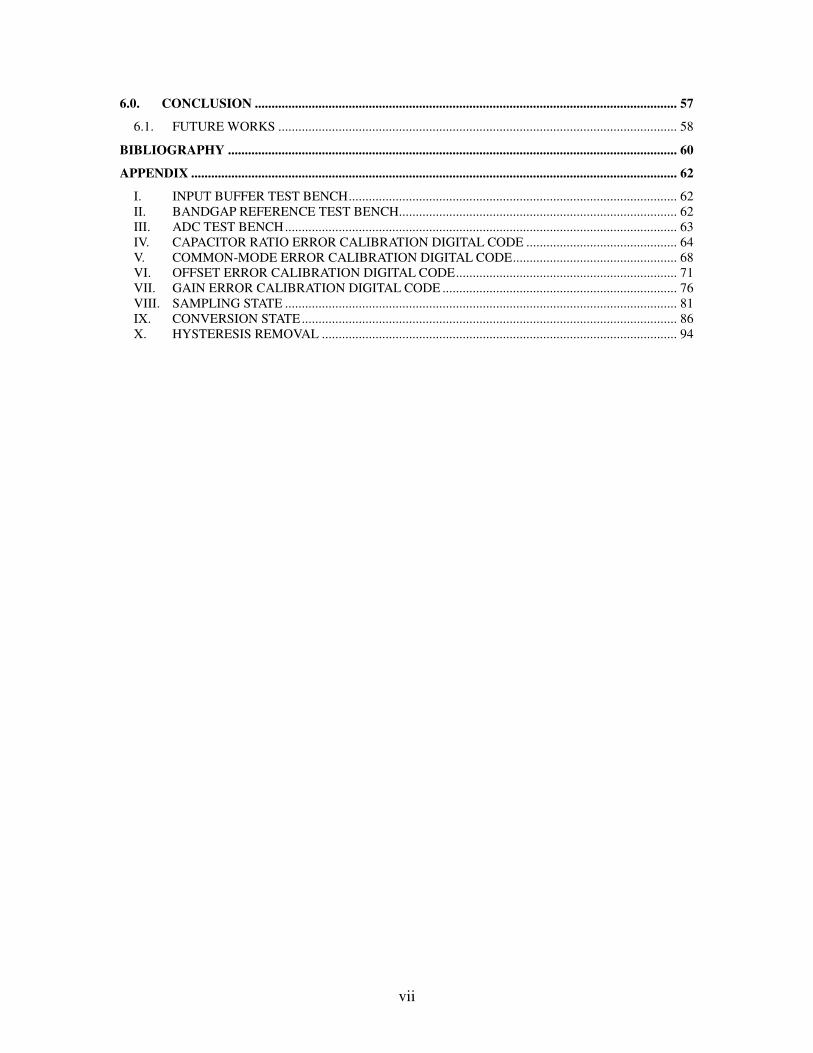
TABLE OF CONTENTS
ACKNOWLEDGEMENT............................................................................................................................ III
ABSTRACT ...................................................................................................................................................V
TABLE OF CONTENTS ........................................................................................................................... VI
LIST OF TABLES ................................................................................................................................... VIII
LIST OF FIGURES.................................................................................................................................... IX
1.0. INTRODUCTION............................................................................................................................ 1
1.1. PROPOSED SOLUTION............................................................................................................... 2 1.2. THESIS ORGANIZATION............................................................................................................ 4
2.0. ANALOG-TO-DIGITAL CONVERTER ARCHITECTURE ..................................................... 5
2.1. DESIGN.......................................................................................................................................... 6 2.2. CONVERSION ALGORITHM...................................................................................................... 9 2.3. DESIGN CHALLENGES..............................................................................................................11
2.3.1. NOISE...................................................................................................................................11 2.3.2. LOW-POWER CONSIDERATION ...................................................................................... 12 2.3.3. ERROR DUE TO PARASITICS AND MISMATCHES ......................................................... 12 2.3.4. PERFORMANCE METRICS ............................................................................................... 13
3.0. CR ADC BUILDING BLOCKS.................................................................................................... 14
3.1. COMPARATOR ........................................................................................................................... 14 3.1.1. FINE COMPARATOR.......................................................................................................... 14 3.1.2. LOW-POWER CONSIDERATIONS FOR THE FINE COMPARATOR ............................... 18 3.1.2. COARSE COMPARATOR.................................................................................................... 21 3.1.3. HYSTERESIS ELIMINATION ALGORITHM ...................................................................... 22
3.2. INPUT BUFFER .......................................................................................................................... 23 3.3. RESISTOR-STRING DACS ........................................................................................................ 25 3.4. REFERENCE VOLTAGE GENERATOR.................................................................................... 26
4.0. SELF-CALIBRATION TECHNIQUES....................................................................................... 28
4.1. CAPACITOR RATIO ERROR CALIBRATION.......................................................................... 28 4.1.1. CRE CALCULATION .......................................................................................................... 29 4.1.2. CRE ERROR REMOVAL..................................................................................................... 31
4.2. COMMON-MODE ERROR (CME) CALIBRATION................................................................. 31 4.2.1. CME ADJUSTMENT SCHEME .......................................................................................... 32 4.2.2. CME CORRECTION CAPACITOR ..................................................................................... 33
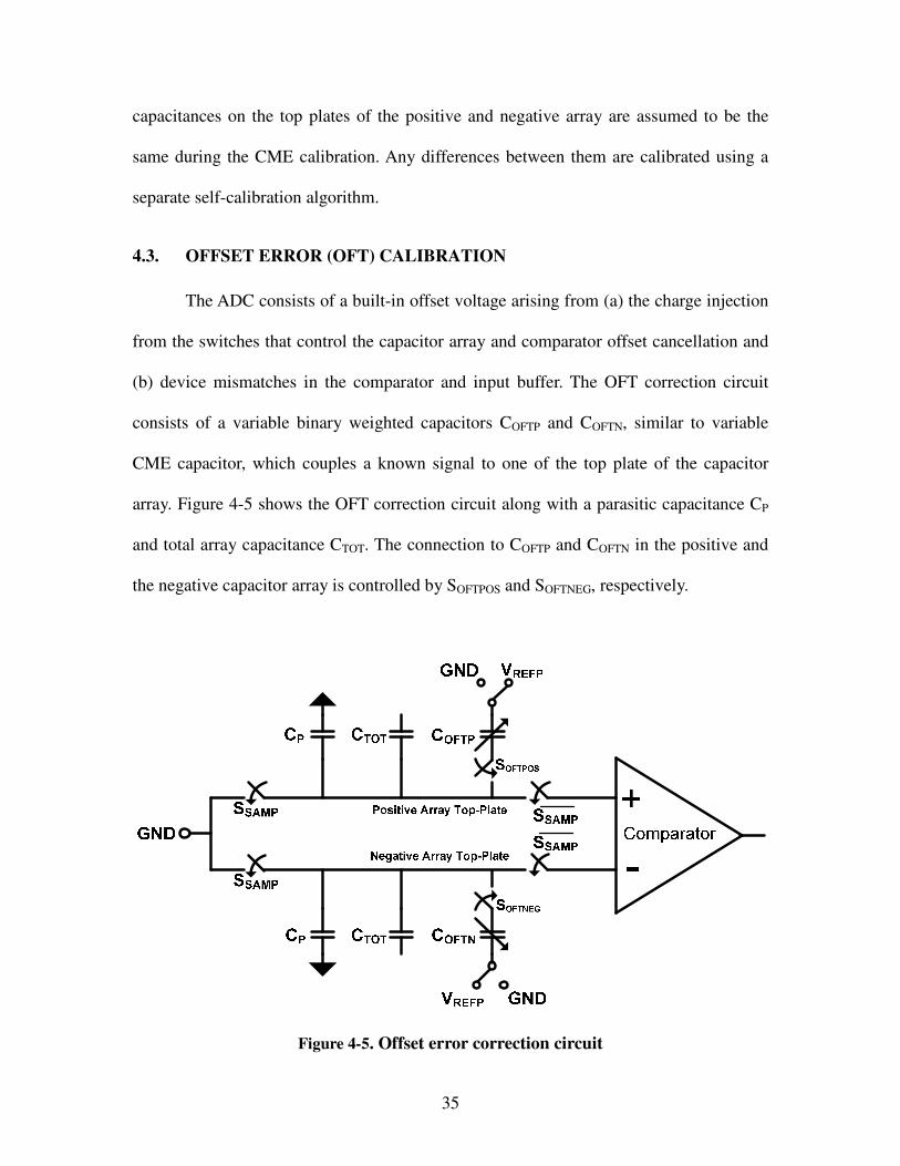
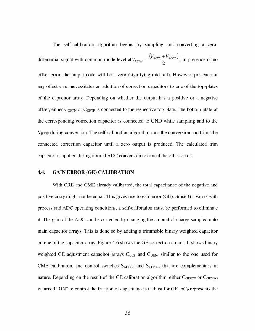
4.3. OFFSET ERROR (OFT) CALIBRATION................................................................................... 35 4.4. GAIN ERROR (GE) CALIBRATION.......................................................................................... 36
5.0. SIMULATION RESULTS............................................................................................................. 39
5.1. INPUT BUFFER .......................................................................................................................... 39 5.2. COMPARATOR ........................................................................................................................... 41 5.3 CRE CALIBRATION................................................................................................................... 45 5.4. CME CALIBRATION .................................................................................................................. 47 5.5. OFT CALIBRATION ................................................................................................................... 47 5.6. GE CALIBRATION ..................................................................................................................... 49 5.7. ADC PERFORMANCE ............................................................................................................... 52
5.7.1. NOISE.................................................................................................................................. 52 5.7.2. POWER ............................................................................................................................... 52 5.7.3. PERFORMANCE METRICS ............................................................................................... 54
vii
6.0. CONCLUSION .............................................................................................................................. 57
6.1. FUTURE WORKS ....................................................................................................................... 58
BIBLIOGRAPHY ...................................................................................................................................... 60
APPENDIX ................................................................................................................................................. 62
I. INPUT BUFFER TEST BENCH.................................................................................................. 62 II. BANDGAP REFERENCE TEST BENCH................................................................................... 62 III. ADC TEST BENCH..................................................................................................................... 63 IV. CAPACITOR RATIO ERROR CALIBRATION DIGITAL CODE ............................................. 64 V. COMMON-MODE ERROR CALIBRATION DIGITAL CODE................................................. 68 VI. OFFSET ERROR CALIBRATION DIGITAL CODE.................................................................. 71 VII. GAIN ERROR CALIBRATION DIGITAL CODE ...................................................................... 76 VIII. SAMPLING STATE ..................................................................................................................... 81 IX. CONVERSION STATE................................................................................................................ 86 X. HYSTERESIS REMOVAL .......................................................................................................... 94
viii
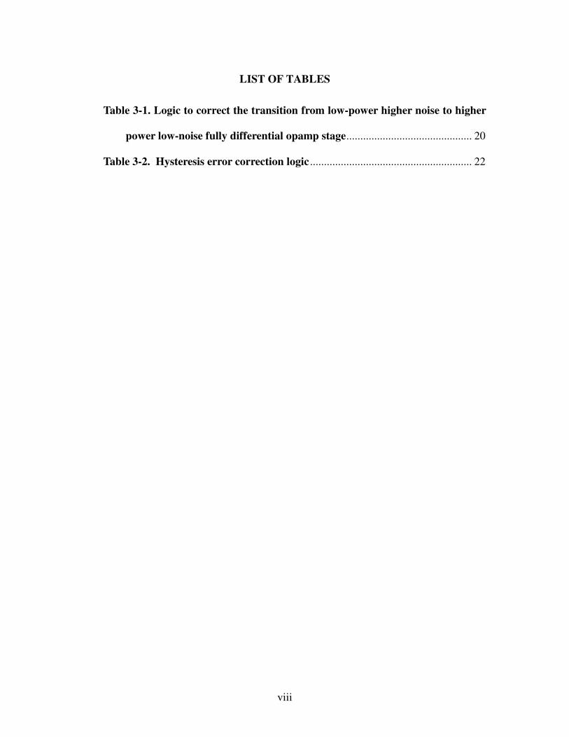
LIST OF TABLES
Table 3-1. Logic to correct the transition from low-power higher noise to higher
power low-noise fully differential opamp stage............................................. 20
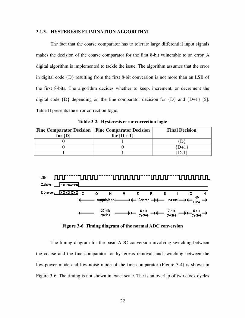
Table 3-2. Hysteresis error correction logic .......................................................... 22
ix
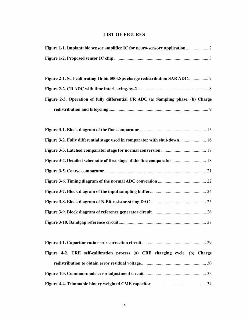
LIST OF FIGURES
Figure 1-1. Implantable sensor amplifier IC for neuro-sensory application .................... 2
Figure 1-2. Proposed sensor IC chip .................................................................................... 3
Figure 2-1. Self-calibrating 16-bit 500kSps charge redistribution SAR ADC.................. 7
Figure 2-2. CR ADC with time interleaving-by-2 ............................................................... 8
Figure 2-3. Operation of fully differential CR ADC (a) Sampling phase. (b) Charge
redistribution and bitcycling......................................................................................... 9
Figure 3-1. Block diagram of the fine comparator ........................................................... 15
Figure 3-2. Fully differential stage used in comparator with shut-down........................ 16
Figure 3-3. Latched comparator stage for normal conversion ........................................ 17
Figure 3-4. Detailed schematic of first stage of the fine comparator............................... 18
Figure 3-5. Coarse comparator........................................................................................... 21
Figure 3-6. Timing diagram of the normal ADC conversion ........................................... 22
Figure 3-7. Block diagram of the input sampling buffer.................................................. 24
Figure 3-8. Block diagram of N-Bit resistor-string DAC ................................................. 25
Figure 3-9. Block diagram of reference generator circuit ................................................ 26
Figure 3-10. Bandgap reference circuit.............................................................................. 27
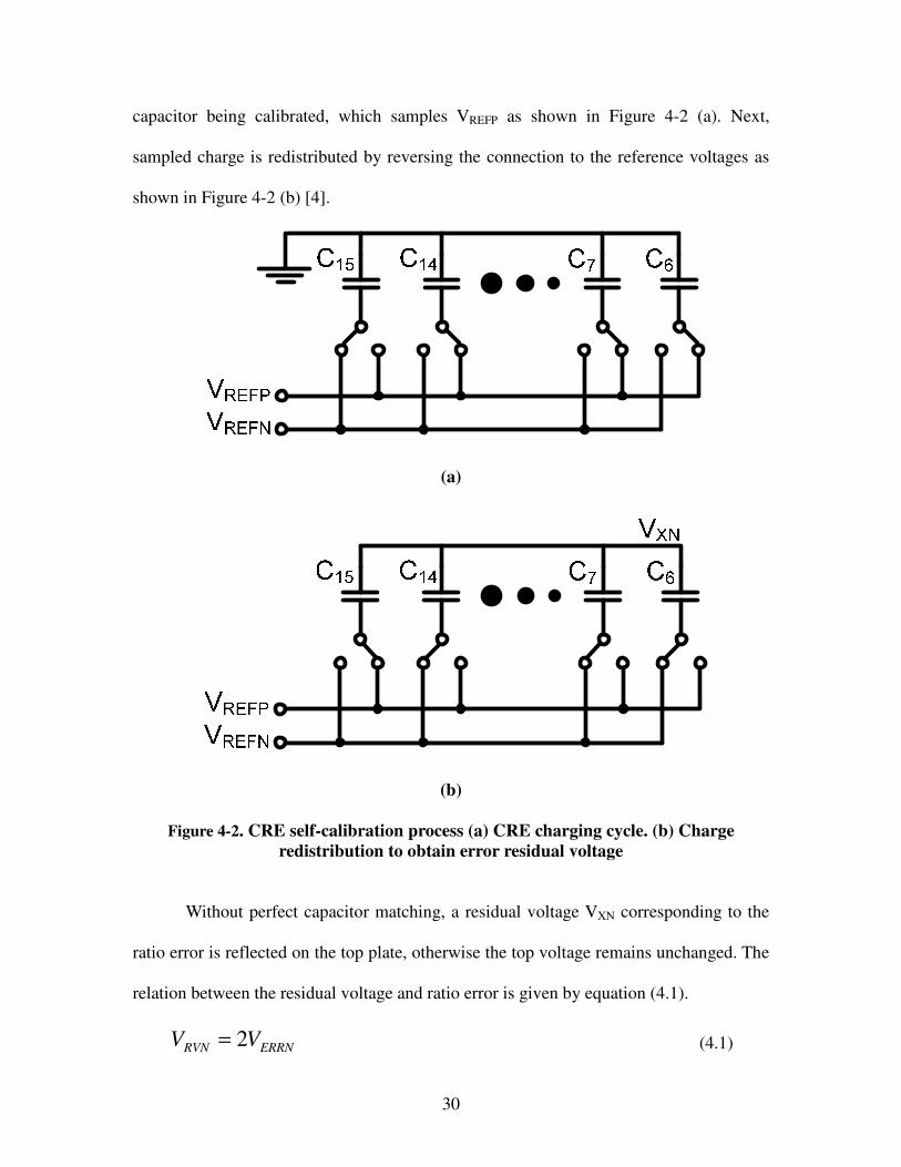
Figure 4-1. Capacitor ratio error correction circuit ......................................................... 29
Figure 4-2. CRE self-calibration process (a) CRE charging cycle. (b) Charge
redistribution to obtain error residual voltage.......................................................... 30
Figure 4-3. Common-mode error adjustment circuit ....................................................... 33
Figure 4-4. Trimmable binary weighted CME capacitor ................................................. 34
x
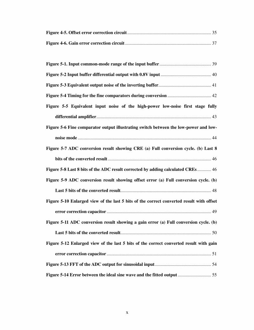
Figure 4-5. Offset error correction circuit ......................................................................... 35
Figure 4-6. Gain error correction circuit ........................................................................... 37
Figure 5-1. Input common-mode range of the input buffer ............................................. 39
Figure 5-2 Input buffer differential output with 0.8V input ............................................ 40
Figure 5-3 Equivalent output noise of the inverting buffer.............................................. 41
Figure 5-4 Timing for the fine comparators during conversion ...................................... 42
Figure 5-5 Equivalent input noise of the high-power low-noise first stage fully
differential amplifier.................................................................................................... 43
Figure 5-6 Fine comparator output illustrating switch between the low-power and low-
noise mode .................................................................................................................... 44
Figure 5-7 ADC conversion result showing CRE (a) Full conversion cycle. (b) Last 8
bits of the converted result .......................................................................................... 46
Figure 5-8 Last 8 bits of the ADC result corrected by adding calculated CREs ............ 46
Figure 5-9 ADC conversion result showing offset error (a) Full conversion cycle. (b)
Last 5 bits of the converted result............................................................................... 48
Figure 5-10 Enlarged view of the last 5 bits of the correct converted result with offset
error correction capacitor ........................................................................................... 49
Figure 5-11 ADC conversion result showing a gain error (a) Full conversion cycle. (b)
Last 5 bits of the converted result............................................................................... 50
Figure 5-12 Enlarged view of the last 5 bits of the correct converted result with gain
error correction capacitor ........................................................................................... 51
Figure 5-13 FFT of the ADC output for sinusoidal input ................................................. 54
Figure 5-14 Error between the ideal sine wave and the fitted output ............................. 55

xi
Dedication
This thesis is dedicated to my parents and my family
who I love dearly
1
1.0. INTRODUCTION
All existing signals in the real world are inherently analog, and that is what
humans understand. However, analog signals are hard to process. Compared to the analog
domain, the digital domain provides easier signal processing, test automation, and offers
programmability. Furthermore, digital circuits demonstrate better tolerance to noise,
supply and process variations. Consequently, there is an incessant need to convert back
and forth between the signals. For such reasons, to interface between the digital
processors and the analog world, data converters are required: analog-to-digital
converters (ADC) to acquire and digitize at the front end and digital-to-analog converters
(DAC) to reproduce the analog signal.
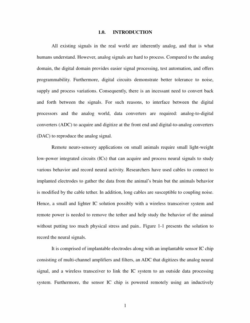
Remote neuro-sensory applications on small animals require small light-weight
low-power integrated circuits (ICs) that can acquire and process neural signals to study
various behavior and record neural activity. Researchers have used cables to connect to
implanted electrodes to gather the data from the animal’s brain but the animals behavior
is modified by the cable tether. In addition, long cables are susceptible to coupling noise.
Hence, a small and lighter IC solution possibly with a wireless transceiver system and
remote power is needed to remove the tether and help study the behavior of the animal
without putting too much physical stress and pain.. Figure 1-1 presents the solution to
record the neural signals.
It is comprised of implantable electrodes along with an implantable sensor IC chip
consisting of multi-channel amplifiers and filters, an ADC that digitizes the analog neural
signal, and a wireless transceiver to link the IC system to an outside data processing
system. Furthermore, the sensor IC chip is powered remotely using an inductively
2
coupled RF telemetry link [1].
Figure 1-1. Implantable sensor amplifier IC for neuro-sensory application
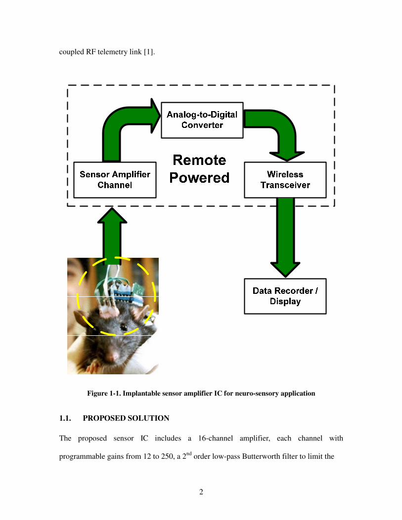
1.1. PROPOSED SOLUTION
The proposed sensor IC includes a 16-channel amplifier, each channel with
programmable gains from 12 to 250, a 2nd
order low-pass Butterworth filter to limit the
3
16:1 Multiplexer
Neural Signal Inputs
Figure 1-2. Proposed sensor IC chip
bandwidth of the analog (neural) signal, a 16:1 multiplexer to select one of the 16
available channels, and a 16-bit 500 ksps ADC to digitize the amplified neural signal [2].
Figure 1-2 shows the proposed system. However, the main focus of this thesis is to
elaborate the design methodology of the 16-bit 500 kSps ADC. The required ADC not
only has to have smaller die area, but also have low noise, low power, high accuracy and
moderate speed.
The design challenges, however, go hand in hand with the advantages of a charge-
redistribution based successive approximation register ADC (CR ADC). The CR ADC
provides a low power solution with high accuracy and high figure-of-merit (FOM) when
compared to other ADC architectures. The CR ADC, however, cannot provide inherent
16-bit accuracy due to device mismatches and parasitics at different nodes. Hence, self-

4
calibration methods have to be implemented to obtain 16-bit accuracy. As mentioned
before, low-power, low-noise, and small area are the requirements of the ADC design and
rest of the thesis focuses on explaining the ADC design and the self-calibration
algorithms.
1.2. THESIS ORGANIZATION
The thesis is organized into 6 chapters. Chapter 2 will discuss the basics of the CR
ADC design while chapter 3 will discuss the designs of various components that
constitute the CR ADC. Chapter 4 will focus on the self-calibration algorithm that helps
eliminate various ADC limitations and errors. Chapter 5 will present the results of the
overall system performance simulations and finally, chapter 6 will comprise the future
direction of the research and end with final thoughts and conclusions.
5
2.0. ANALOG-TO-DIGITAL CONVERTER ARCHITECTURE
Analog-to-digital converters (ADCs) are required to acquire and digitize the
analog signals for easier data processing in the digital domain, for automating test and for
programmability. Different ADC architectures are available on the market, depending on
system requirements. For a neuro-sensory application where a low power ADC with
small area, good resolution and accuracy is required, successive approximation register
(SAR) ADC architecture is selected. The SAR ADCs are popular for their low power
consumption, decent size, high resolution, accuracy and small FOM factor. Pipeline
ADCs dissipate more power than SAR ADCs at 500 KSps but are better at higher
sampling rates. Flash ADC requires many comparators which add up to more power and
area even though speed can be very high. It is difficult to use a delta-sigma ADC with
multiplexed input signals and the requirement of 500 KSps is somewhat high for a delta-
sigma to achieve low power dissipation with its need to oversample the input.
The SAR ADC converts an analog signal into a digital code using a binary search
algorithm in a feedback loop including a 1-bit ADC (comparator). It consists of a sample
and hold circuit to acquire the input signal, an internal reference DAC, a comparator that
compares the input signal to the output of the internal DAC, a SAR to hold the
approximate digital representation feeding the internal DAC. Out of numerous SAR ADC
architectures that are available, a fully differential charge redistribution based SAR ADC
(CR ADC) is implemented to meet the design specifications. The 16-bit 500 KSps CR
ADC is designed in a 0.25µm CMOS process.
6
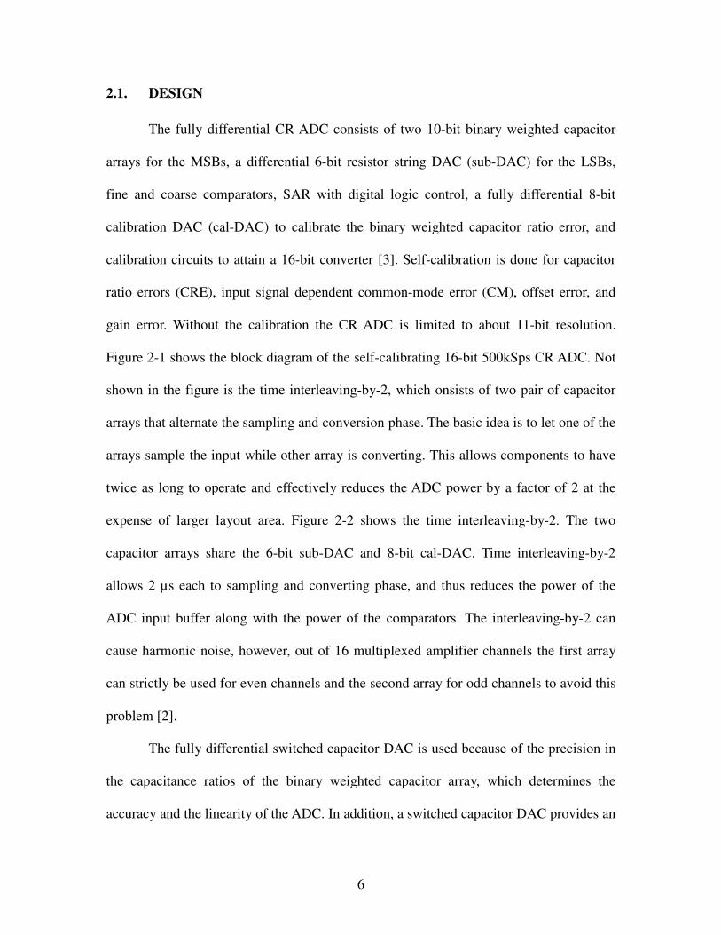
2.1. DESIGN
The fully differential CR ADC consists of two 10-bit binary weighted capacitor
arrays for the MSBs, a differential 6-bit resistor string DAC (sub-DAC) for the LSBs,
fine and coarse comparators, SAR with digital logic control, a fully differential 8-bit
calibration DAC (cal-DAC) to calibrate the binary weighted capacitor ratio error, and
calibration circuits to attain a 16-bit converter [3]. Self-calibration is done for capacitor
ratio errors (CRE), input signal dependent common-mode error (CM), offset error, and
gain error. Without the calibration the CR ADC is limited to about 11-bit resolution.
Figure 2-1 shows the block diagram of the self-calibrating 16-bit 500kSps CR ADC. Not
shown in the figure is the time interleaving-by-2, which onsists of two pair of capacitor
arrays that alternate the sampling and conversion phase. The basic idea is to let one of the
arrays sample the input while other array is converting. This allows components to have
twice as long to operate and effectively reduces the ADC power by a factor of 2 at the
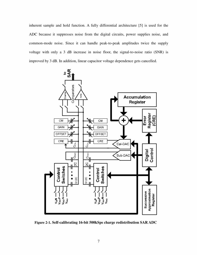
expense of larger layout area. Figure 2-2 shows the time interleaving-by-2. The two
capacitor arrays share the 6-bit sub-DAC and 8-bit cal-DAC. Time interleaving-by-2
allows 2 µs each to sampling and converting phase, and thus reduces the power of the
ADC input buffer along with the power of the comparators. The interleaving-by-2 can
cause harmonic noise, however, out of 16 multiplexed amplifier channels the first array
can strictly be used for even channels and the second array for odd channels to avoid this
problem [2].
The fully differential switched capacitor DAC is used because of the precision in
the capacitance ratios of the binary weighted capacitor array, which determines the
accuracy and the linearity of the ADC. In addition, a switched capacitor DAC provides an
7
inherent sample and hold function. A fully differential architecture [5] is used for the
ADC because it suppresses noise from the digital circuits, power supplies noise, and
common-mode noise. Since it can handle peak-to-peak amplitudes twice the supply
voltage with only a 3 dB increase in noise floor, the signal-to-noise ratio (SNR) is
improved by 3 dB. In addition, linear capacitor voltage dependence gets cancelled.
Figure 2-1. Self-calibrating 16-bit 500kSps charge redistribution SAR ADC
8
Figure 2-2. CR ADC with time interleaving-by-2
9
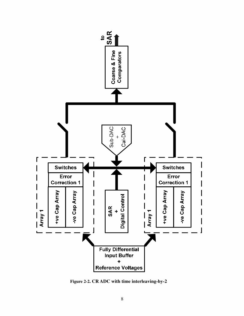
2.2. CONVERSION ALGORITHM
(a)
(b)
Figure 2-3. Operation of fully differential CR ADC (a) Sampling phase. (b) Charge
redistribution and bitcycling
The operation of a conventional fully differential CR ADC is shown in Figure 2-3.
The CR ADC consists of a two identical capacitor arrays connected to the differential
comparator input. The conversion begins by sampling a differential input signal, VINP and
VINN, onto the bottom plates of two binary weighted capacitors arrays as shown in Figure
10
2-3 (a). The top-plates of the capacitors are grounded during sampling and the
comparator is put in reset mode. Furthermore, the inputs of the comparator are isolated
from the top-plates of the capacitor arrays. This modified sampling technique helps
eliminate the effects of DC offset voltage of the comparator, which otherwise will be
sampled on the capacitor array during input acquisition phase. The comparator is taken
out of reset after the sampling is completed. It should be noted that by selecting the
comparator reset potential to be mid-voltage of the positive and negative reference
signals, the comparator contribution to the top-plate parasitic as seen by common-mode
signals is reduced [6].
After the sampling phase is complete, the CR ADC enters the charge
redistribution and bit-cycling phase as shown in Figure 2-3 (b).The MSB capacitor of the
positive capacitor array is connected to positive voltage reference VREFP, while the rest of
the capacitors including CDAC are connected to negative voltage reference VREFN.
Depending on whether the comparator outputs “1” or “0,” the MSB capacitor is kept
connected to VREFP or connected to VREFN. Then next MSB is connected to VREFP and
same procedure is repeated for the first 10 MSB bits. Identical steps are performed on the
negative capacitor array (not shown in figures) as well, but with opposite reference
voltages. The 6 LSB bits are controlled by a fully differential resistor-string 6-bit sub-
DAC as depicted in Figure 2-1. The sub-DAC adds or subtracts charge through CDAC
depending on the digital logic that controls the LSB bits.
The connections of the bottom plates of both capacitor arrays are controlled by
digital logic. Moreover, the designed CR ADC constitutes a coarse comparator and a fine
comparator that can switch between low power mode with higher noise mode and high
11
power mode with lower noise. The coarse comparator handles the large voltage levels
while the fine comparator handles only small voltage levels to avoid hysteresis and has
higher resolution. The comparator design is discussed in detail in Chapter 3.
2.3. DESIGN CHALLENGES
The low power and high accuracy requirement for the neuro-sensory application
poses several design challenges to the CR ADC. The requirement of 16-bit resolution has
to be met with a system that is both low power and low noise, plus there are device
mismatches and parasitics that need to be reduced or eliminated. These issues are
addressed in detail in later chapters. This section endeavors to introduce the various
sources of error and includes brief discussions about possible solutions.
2.3.1. NOISE
There are four major sources of noise in the CR ADC, the input buffer noise, the
high-speed comparator noise, the kT/C noise due to switches and capacitor arrays, and
reference generator noise. The input buffer can be designed with larger input devices with
high first stage gain to lower thermal noise and flicker noise. The high-speed
comparator’s noise might cause errors in LSB conversions. The comparator circuit can be
designed with a cascade of capacitively coupled multiple low-gain stages [6] that cancel
offset voltages. The first gain stage of the fine comparator can be designed with large
input devices biased at higher current to minimize the flicker and thermal noise. The
noise from the reference generator circuit can be filtered using a large external capacitor
that helps limit the noise bandwidth. The kT/C noise can be reduced by increasing the
capacitor array sizes. However, large capacitor sizes aggravate the settling time and
12
conversion speed. So the capacitor sizes have to be carefully selected.
2.3.2. LOW-POWER CONSIDERATION
The majority of power consumption results from amplifiers driving large
capacitive or small resistor loads, reducing the thermal noise, increasing speed, and to
reduce settling times. These interrelated factors necessitate that the design considers the
trade-offs and seek more optimal solutions. For instance, the amplifiers should dissipate
the minimal possible power required to drive their load. A design technique can be used
where a low-power stage with higher noise can replace a higher power low-noise stage
during a time when low-noise is not as critical such as during the MSB conversion, which
does not require high accuracy. Other technique, such as shutting down amplifiers, when
they are not in use can also be implemented. As discussed earlier, the ADC incorporates a
time interleaving-by-2 technique to reduce average power by a factor of two.
2.3.3. ERROR DUE TO PARASITICS AND MISMATCHES
The mismatches among the binary-weighted capacitor ratios, the parasitics on the
capacitor array top plates and the comparator stages, mismatches in the total capacitance
between the positive and negative capacitor arrays, mismatches in the input differential
stages of amplifiers and charge-injection due to switch turn-off transitions can limit the
accuracy of the ADC. Therefore, self-calibrating schemes are introduced to eliminate the
capacitor ratio errors, the common-mode errors caused by parasitics on the top plate, the
gain error caused by the difference in total capacitance of the positive and negative
capacitor arrays, and the offset voltages caused by charge-injection and device
mismatches in the comparator circuit. Furthermore, larger devices and common-centroid
13
layout techniques can be implemented to reduce the mismatches.
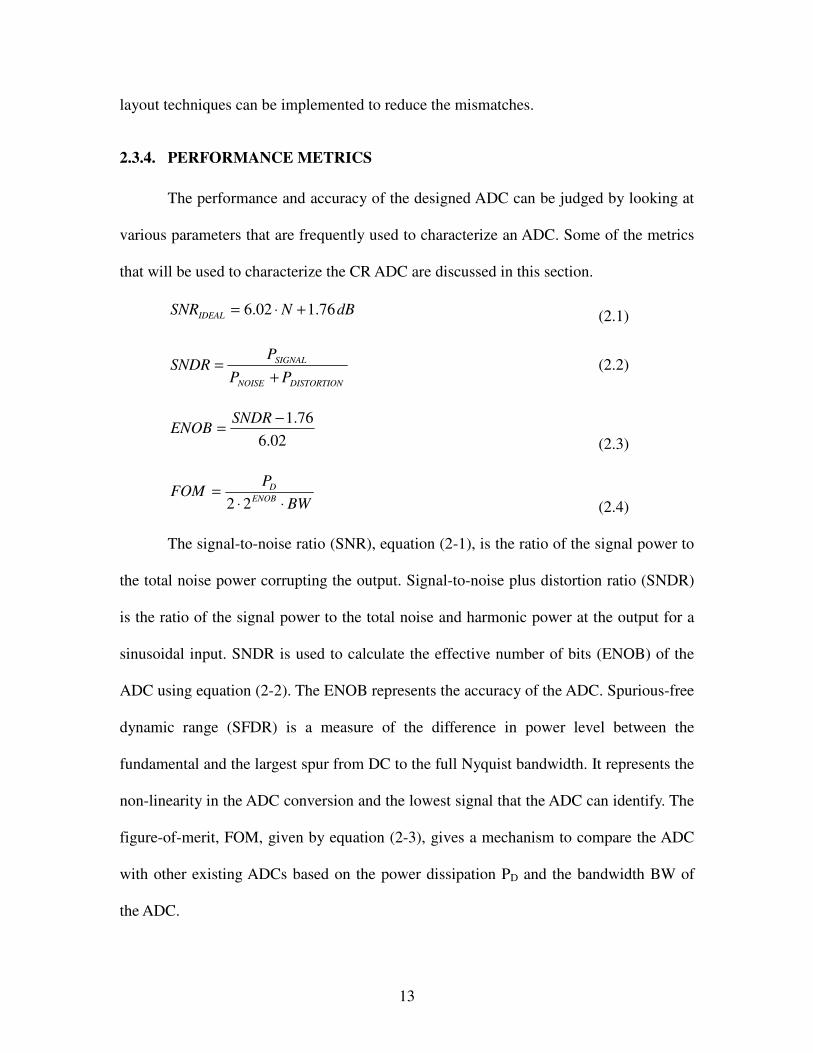
2.3.4. PERFORMANCE METRICS
The performance and accuracy of the designed ADC can be judged by looking at
various parameters that are frequently used to characterize an ADC. Some of the metrics
that will be used to characterize the CR ADC are discussed in this section.
dBNSNRIDEAL 76.102.6 +⋅= (2.1)
DISTORTIONNOISE
SIGNAL
PP
PSNDR
+= (2.2)
02.6
76.1−=
SNDRENOB
(2.3)
BW
PFOM
ENOB
D
⋅⋅=
22 (2.4)
The signal-to-noise ratio (SNR), equation (2-1), is the ratio of the signal power to
the total noise power corrupting the output. Signal-to-noise plus distortion ratio (SNDR)
is the ratio of the signal power to the total noise and harmonic power at the output for a
sinusoidal input. SNDR is used to calculate the effective number of bits (ENOB) of the
ADC using equation (2-2). The ENOB represents the accuracy of the ADC. Spurious-free
dynamic range (SFDR) is a measure of the difference in power level between the
fundamental and the largest spur from DC to the full Nyquist bandwidth. It represents the
non-linearity in the ADC conversion and the lowest signal that the ADC can identify. The
figure-of-merit, FOM, given by equation (2-3), gives a mechanism to compare the ADC
with other existing ADCs based on the power dissipation PD and the bandwidth BW of
the ADC.
14
3.0. CR ADC BUILDING BLOCKS
3.1. COMPARATOR
A fast and high resolution ADC requires a high-performance comparator,
essentially a 1-bit ADC. The comparator compares two analog signals and outputs a
binary digital output. The comparator used in the ADC not only has to be fast and have
high resolution but also need to consume low power and have low noise. There are many
hurdles that the comparator needs to overcome. Firstly, the comparator precision must be
greater than ADC resolution during self-calibration mode (calibrating for errors). This
puts a limit on the noise of the comparator. Secondly, the comparator must avoid
hysteresis in the threshold voltage of the comparator input stage due to large differential
signals during conversion. To deal with this voltage stress, a dual comparator topology as
shown in Figure 2-1 is used [5]. The basic idea is to use a coarse comparator to convert
the input early in successive approximation when the voltage stress on MOS devices are
greatest, then use a fine comparator to resolve smaller voltage levels that require more
comparator precision. These two design challenges are discussed more thoroughly in
forthcoming subsections along with various techniques to reduce power and increase gain
and speed.
3.1.1. FINE COMPARATOR
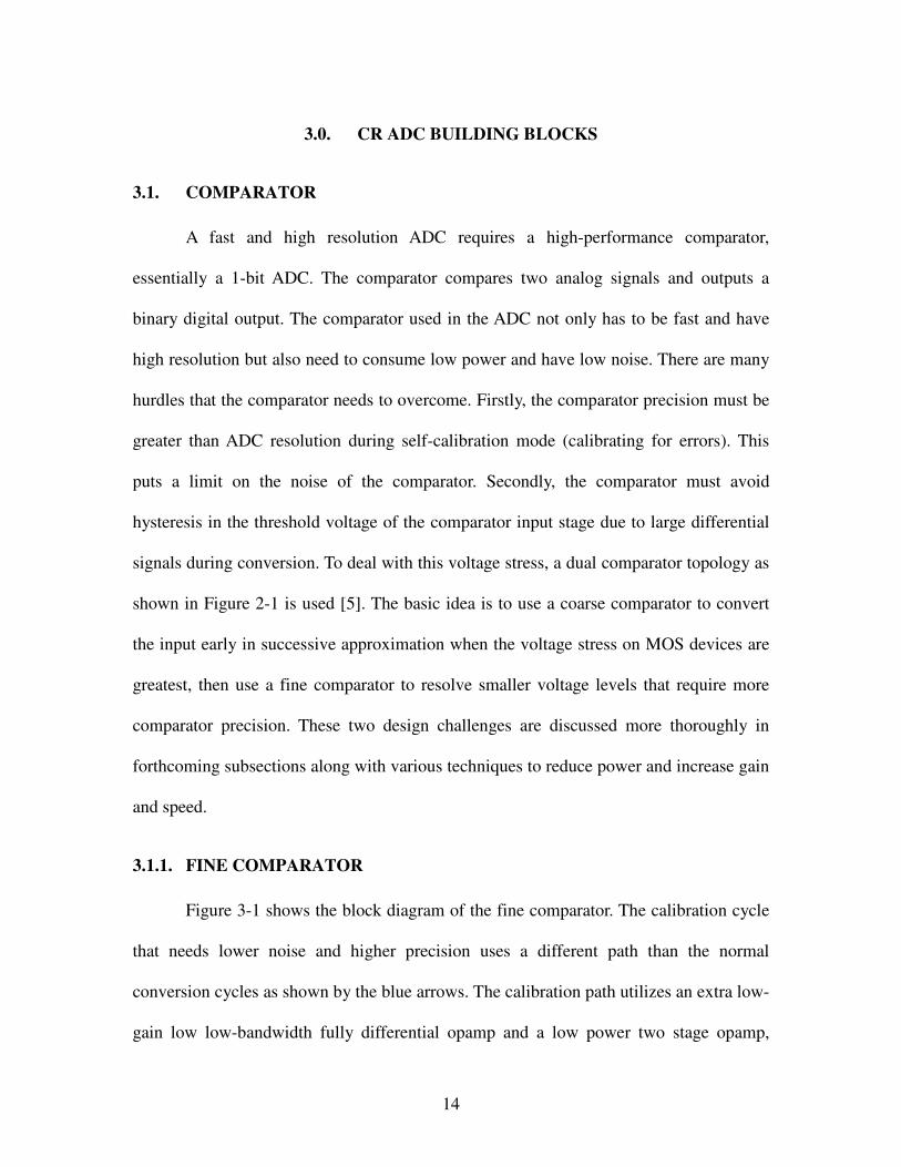
Figure 3-1 shows the block diagram of the fine comparator. The calibration cycle
that needs lower noise and higher precision uses a different path than the normal
conversion cycles as shown by the blue arrows. The calibration path utilizes an extra low-
gain low low-bandwidth fully differential opamp and a low power two stage opamp,
15
while the normal conversion implements a latched-comparator for high speed
performance. Each path shares first two low-gain fully differential opamp stages.
Switched capacitors, comprising of C1, C2 and C3, are used between each stages; the
reset switches presets the bias on the inputs of each stage during sampling. The reset
switches are sequentially turned-off (from R1-R4) to cancel the input-referred offset
caused by charge injection due to switch turn-off, by storing the offset in the capacitors
[6]. Furthermore, the capacitors help reduce the flicker noise due from to the opamp
stages [10].
+
-
-+
+
-
-+
+
-
-+
+
-
-+
+
-
R1
R1
R3
R3
R4
R4
R2
R2
CalnCaln
Latch
Comparator
C1 C2
C3
OUT-
OUT+
OUT
1st StageFully Differential
2nd StageFully Differential
Calibration
Conversion
3rd StageFully Differential
2-stage
Figure 3-1. Block diagram of the fine comparator
Only one of the paths is activated during the calibration or the normal conversion
cycle. The latched-comparator is disabled during the calibration cycle by pulling the latch
16
control signal low, whereas calibration switches “Caln” are turned off during normal
conversion. The extra two stages of the calibration path are shut-down during conversion
to save power. The shut-down signals do not turn off the opamp completely, but shuts off
the large current path to lessen power.
OUT-
OUT+
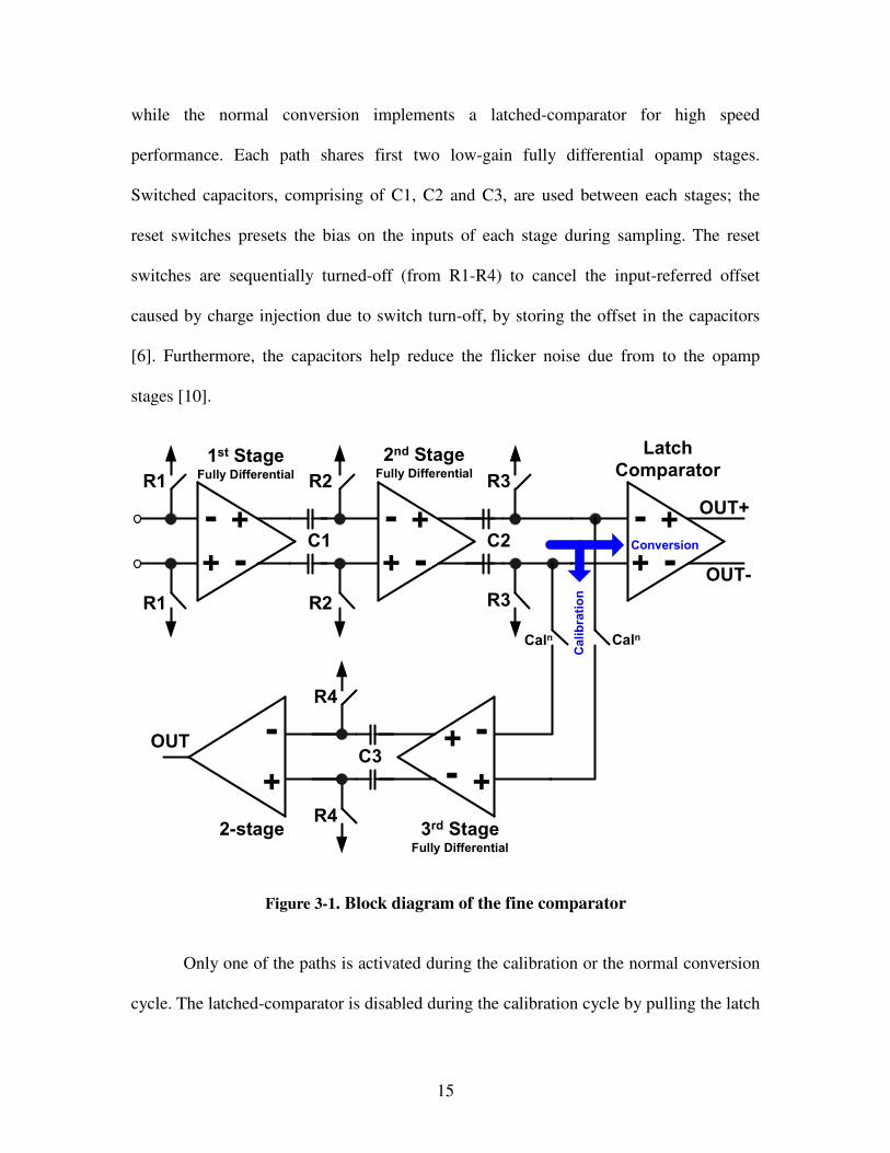
Figure 3-2. Fully differential stage used in comparator with shut-down
Figure 3-2 presents the schematic of the fully differential opamp used in the 1st,
2nd
, and 3rd
stages of the comparator [6]. The opamp consists of an nMOS differential
input pair, selected for higher speed, diode connected loads M11 and M22, to get the
desired gain, cross-coupled positive feedback transistors M12 and M21, for gain
enhancement, and output stages comprising of MOP1, MOP2, MON1 and MON2 for additional
gain and output level shifting to mid-rail level. The positive feedback can be used for
increasing gain because the amplifiers need not be linear and can work in open-loop
17
configuration [9]. The nMOS differential stage is implemented as the fine comparator
only sees smaller voltage level, and hence hysteresis is not an issue. The shut-down
signal SD is implemented to turn on the current source with W/L ratios k×m, with m
being the W/L ratio of the current source kept on all the time.
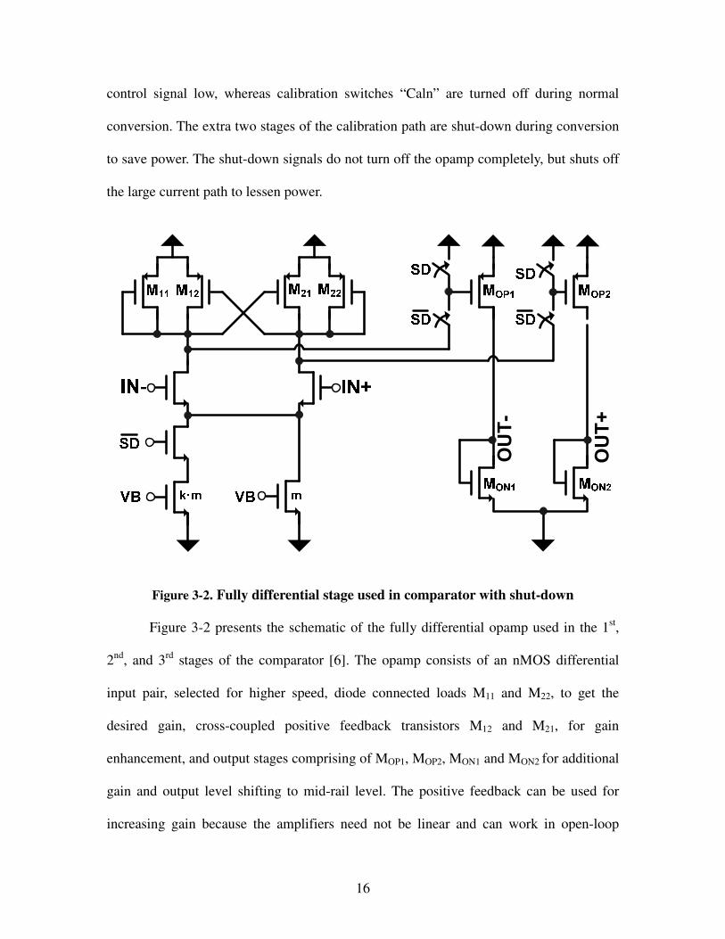
Figure 3-3. Latched comparator stage for normal conversion
The fact that the CR ADC operates at 20-MHz clock rate necessitates the usage of
the latched-comparator for high-speed performance. Figure 3-3 depicts the schematic of a
latched-comparator [8]. It consists of a pMOS differential input stage, a CMOS flip-flop
stage, and an S-R latch. The differential input stage acts as a preamplifier to amplify the
input signals. The CMOS flip-flop stage contains a flip-flop, M2A and M2B, and nMOS
pass-gates M3A and M3B for strobing, and nMOS switch M2 for resetting the comparator.
Devices M4A, M4B, M5A, and M5B are used to precharge the drain nodes to the positive
power supply during reset and also perform as flip-flops during the latch phase. The
18
switch M2 equalizes the node voltages across it during initial reset phase, and after the
input decision is settled, a voltage difference corresponding to the inputs is stored across
the same nodes. The inequity in these nodes triggers the positive feedback circuit (M5A,
and M5B), and this feedback circuit along with M3A and M3B amplifies the voltage
difference to the power supply voltage. The S-R latch outputs the fully complementary
latched signal at the end of latch phase and holds on to the previous value during reset.
The clock signals Φ1 and Φ2 are non-overlapping clocks.
3.1.2. LOW-POWER CONSIDERATIONS FOR THE FINE COMPARATOR
Figure 3-4. Detailed schematic of first stage of the fine comparator
Low-power consumption is the foremost requirement of the ADC design. The
optimization of each opamp stage by finding a proper balance between power, noise,
speed, and area is not adequate for low-power design. Therefore, various other design
19
techniques are exploited to lower power dissipation. The first stage poses as the main
noise source in comparator; therefore, larger current and large device geometry are used
to lower the thermal and flicker noise. As can be seen in equation (3-1), increasing
current lowers the thermal noise by increasing the transconductance of the MOS devices
(1st term in the equation), and larger devices lower flicker noise (2
nd term in the equation)
[12]. The equation provides the total squared input-referred noise of the MOS device.
cOXm fLWC
K
gkTinVn
•••+
•=
3
24, 2
(3-1)
The technique shown in Figure 3-4 is exploited to reduce the average power
consumption of the comparator. Two parallel opamps, one with low-power and the other
with low-noise, are used in the first stage. While one parallel stage is operating, the other
stage is disabled and shut-down to lower the average power consumption. Referring back
to Figure 3-2, when not in use the respective opamp is shut-down by pulling the gate of
the current source to VDD (for pMOS source) and disconnecting the switch, which
connects the differential stage source to the current source, to turn-off high current path
(for nMOS source). The shut-down switch is introduced in series with the current source
instead of gating the current source to limit the droop in the bias voltage caused by
transient switching. Large capacitors have to be introduced if the current source is gated
to limit the droop in voltage bias, which puts slew-rate limitation on bias voltage
restoration. Since noise is important for the LSB bits, a low-noise higher-power opamp is
used for last 3 LSBs. For higher LSBs (remaining 5-bits), the low-power opamp is used.
The transition between the low-power and low-noise opamps requires an adjustment in
digital control during the conversion cycle. Table I shows the logic to correct the possible
20
conversion error before the low-noise transition.
Table 3-1. Logic to correct the transition from low-power higher noise to higher
power low-noise fully differential opamp stage
Low-noise Decision
for D
Low-noise Decision
for D + 1
Low-noise Decision
for D - 1
Final
Decision
1 0 --- {D}
1 1 --- {D+1}
0 --- 0 {D-1}
0 --- 1 {D}
The higher noise of the low-power opamp version may result in wrong
conversion. The error can be corrected in the digital domain if its magnitude is within the
range of the correction algorithm. The error, if present, is assumed to be within an LSB of
the first 13 bits converted. It means that if {D} represents the converted digital code from
the first 13 bits, then the correct result is within {D+1} and {D-1}. The error correction
involves one extra low-noise comparator conversion and increment/decrement counters.
Depending on the decision of {D} the SAR either increments or decrements the counter.
If the decision of {D} is “1,” it signifies that the correct bit can either be {D} or
{D+1}. Therefore, a secondary conversion is performed using {D+1} applied to the
DAC. If the secondary decision is “0,” inferring that the voltage level is within the
respective LSB, the digital code {D} is maintained and the remaining bits are converted.
The decision “1” infers that the decision {D} is small when compared to the
corresponding LSB level, thus {D} is incremented before completing the conversion. If,
however, the primary decision of {D} is “0,” it signifies that the correct bit can either be
{D} or {D-1}. A secondary conversion with the digital code {D-1} is performed in that
case to determine whether the digital code from the first 13 bits should be kept or
decremented.
21
3.1.2. COARSE COMPARATOR
The coarse and fine comparators are implemented to eliminate the hysteresis
problem introduced due to large differential signals. Since the coarse comparator resolves
high input levels, it consists of a pMOS differential input stage at the input. The pMOS
devices are inherently resistant to hysteresis when compared to the nMOS devices [2]
Figure 3-5 shows the block diagram of the coarse comparator.
+
-
-+
+
-
-+
R1
R1 R2
R2
C
IN+
IN-OUT+
OUT-
Latch
Comparator
Fully
Differential
Figure 3-5. Coarse comparator
It consists of a low-gain fully differential opamp stage followed by a latched-
comparator stage. The fully differential opamp stage and latched-comparator utilizes the
same architecture as the respective fine comparator stages. The low-gain opamp stage
helps isolate the main capacitor arrays from the switching noise of the latched-
comparator. The capacitor C is used for offset cancellation as previously discussed. To
reduce the average power consumption, the fully differential opamp stage implements a
shut-down signal.
22
3.1.3. HYSTERESIS ELIMINATION ALGORITHM
The fact that the coarse comparator has to tolerate large differential input signals
makes the decision of the coarse comparator for the first 8-bit vulnerable to an error. A
digital algorithm is implemented to tackle the issue. The algorithm assumes that the error
in digital code {D} resulting from the first 8-bit conversion is not more than an LSB of
the first 8-bits. The algorithm decides whether to keep, increment, or decrement the
digital code {D} depending on the fine comparator decision for {D} and {D+1} [5].
Table II presents the error correction logic.
Table 3-2. Hysteresis error correction logic
Fine Comparator Decision
for {D}
Fine Comparator Decision
for {D + 1}
Final Decision
0 1 {D}
0 0 {D+1}
1 1 {D-1}
Figure 3-6. Timing diagram of the normal ADC conversion
The timing diagram for the basic ADC conversion involving switching between
the coarse and the fine comparator for hysteresis removal, and switching between the
low-power mode and low-noise mode of the fine comparator (Figure 3-4) is shown in
Figure 3-6. The timing is not shown in exact scale. The is an overlap of two clock cycles
23
between the acquisition phase, the coarse conversion phase, the low-power fine
comparator conversion phase, and the low-noise fine comparator conversion phase. The
overlap represents the two extra clock cycles used to power-up and reset the
corresponding comparator. The low-power fine comparator mode utilizes seven clock
cycles for converting 5 LSB bits and implementing hysteresis removal algorithm. The
low-noise fine comparator mode converts 3rd
LSB bit twice to remove possible LSB error
from previous conversion and rest of LSBs. One extra clock cycle represent the reset
phase to reset the fine comparator when switching between the low-power and low-noise
fine comparator modes.
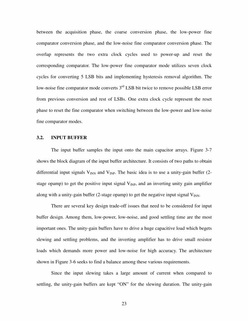
3.2. INPUT BUFFER
The input buffer samples the input onto the main capacitor arrays. Figure 3-7
shows the block diagram of the input buffer architecture. It consists of two paths to obtain
differential input signals VINN and VINP. The basic idea is to use a unity-gain buffer (2-
stage opamp) to get the positive input signal VINP, and an inverting unity gain amplifier
along with a unity-gain buffer (2-stage opamp) to get the negative input signal VINN.
There are several key design trade-off issues that need to be considered for input
buffer design. Among them, low-power, low-noise, and good settling time are the most
important ones. The unity-gain buffers have to drive a huge capacitive load which begets
slewing and settling problems, and the inverting amplifier has to drive small resistor
loads which demands more power and low-noise for high accuracy. The architecture
shown in Figure 3-6 seeks to find a balance among these various requirements.
Since the input slewing takes a large amount of current when compared to
settling, the unity-gain buffers are kept “ON” for the slewing duration. The unity-gain
24
buffers are designed to supply adequate current to slew to within 1% of the maximum
input amplitude. Referring to Figure 3-7, the blue colored wire highlights the slewing
path. During the remainder of the sampling time, the output buffer from the sensor
amplifier channel directly charges the capacitance CT.
Figure 3-7. Block diagram of the input sampling buffer
During the signal settling, the unity-gain buffers are completely shut down, so that
average power is reduced dramatically. The red colored wire highlights the settling path.
The noise of the unity-gain buffers need not be low as they are used for slewing purpose
only. However, the negative differential input is controlled by the inverting amplifier
during both slewing and settling. Therefore, the noise of this amplifier is critical to the
input buffer performance. So the inverting amplifier is designed to have low-noise. Large
resistors cannot be used to set the gain as resistors have thermal noise, hence, the opamp
has to provide large output currents to drive the small feedback resistor and reduce its
noise. The design is optimized by keeping the switch parasitics connected to the main
25
capacitor array in mind.
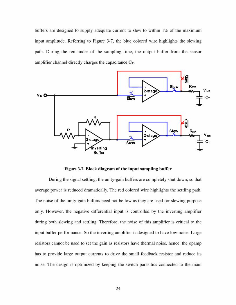
3.3. RESISTOR-STRING DACS
Figure 3-8. Block diagram of an N-Bit resistor-string DAC
The DACs are used in the CR ADC to convert the last 6 LSB bits and to calibrate
for CRE generated from binary ratio mismatches among capacitors in the capacitor
arrays. Various architectures including current-steering DACs, R-2R ladder DACs, and
charge-scaling DACs composed of binary weighted capacitors exist for those purposes.
The resistor-string DAC is selected because it is a relatively easy design with smaller area
and decent speed when compared to charge-scaling DAC and other architectures. A
simple differential N-bit resistor-string DAC requires 2N resistors in series and control
switches to tap one of the equal 2N voltage segments of the resistor divider network. The
6-bit sub-DAC utilizes a single stage 6:64 decoder to select one of voltage segments. The
26
8-bit cal-DAC uses a tree-like decoder whereby the first 4 bits control switches produce
16 voltage levels and the second 4 bits control switches multiplex one of these voltage
levels to the output [11]. The DAC produces differential outputs. Figure 3-8 shows a
block diagram of the N-bit resistor string DAC. The MOS switches types and sizes in the
multiplexers are carefully selected to provide optimal speed performance.
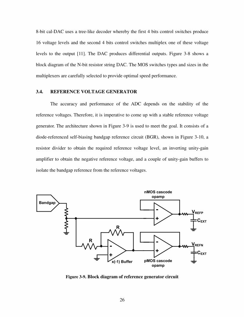
3.4. REFERENCE VOLTAGE GENERATOR
The accuracy and performance of the ADC depends on the stability of the
reference voltages. Therefore, it is imperative to come up with a stable reference voltage
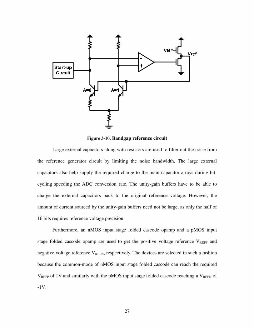
generator. The architecture shown in Figure 3-9 is used to meet the goal. It consists of a
diode-referenced self-biasing bandgap reference circuit (BGR), shown in Figure 3-10, a
resistor divider to obtain the required reference voltage level, an inverting unity-gain
amplifier to obtain the negative reference voltage, and a couple of unity-gain buffers to
isolate the bandgap reference from the reference voltages.
+
-+
-
+
-
Bandgap
R
R
CEXT
CEXT
VREFP
VREFN
nMOS cascode
opamp
x(-1) Buffer pMOS cascode
opamp
Figure 3-9. Block diagram of reference generator circuit
27
Figure 3-10. Bandgap reference circuit
Large external capacitors along with resistors are used to filter out the noise from
the reference generator circuit by limiting the noise bandwidth. The large external
capacitors also help supply the required charge to the main capacitor arrays during bit-
cycling speeding the ADC conversion rate. The unity-gain buffers have to be able to
charge the external capacitors back to the original reference voltage. However, the
amount of current sourced by the unity-gain buffers need not be large, as only the half of
16 bits requires reference voltage precision.
Furthermore, an nMOS input stage folded cascode opamp and a pMOS input
stage folded cascode opamp are used to get the positive voltage reference VREFP and
negative voltage reference VREFN, respectively. The devices are selected in such a fashion
because the common-mode of nMOS input stage folded cascode can reach the required
VREFP of 1V and similarly with the pMOS input stage folded cascode reaching a VREFN of
-1V.
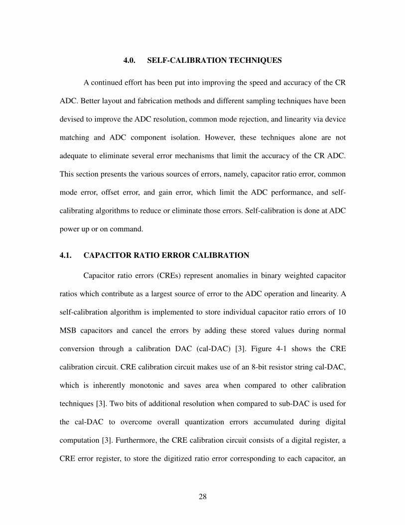
28
4.0. SELF-CALIBRATION TECHNIQUES
A continued effort has been put into improving the speed and accuracy of the CR
ADC. Better layout and fabrication methods and different sampling techniques have been
devised to improve the ADC resolution, common mode rejection, and linearity via device
matching and ADC component isolation. However, these techniques alone are not
adequate to eliminate several error mechanisms that limit the accuracy of the CR ADC.
This section presents the various sources of errors, namely, capacitor ratio error, common
mode error, offset error, and gain error, which limit the ADC performance, and self-
calibrating algorithms to reduce or eliminate those errors. Self-calibration is done at ADC
power up or on command.
4.1. CAPACITOR RATIO ERROR CALIBRATION
Capacitor ratio errors (CREs) represent anomalies in binary weighted capacitor
ratios which contribute as a largest source of error to the ADC operation and linearity. A
self-calibration algorithm is implemented to store individual capacitor ratio errors of 10
MSB capacitors and cancel the errors by adding these stored values during normal
conversion through a calibration DAC (cal-DAC) [3]. Figure 4-1 shows the CRE
calibration circuit. CRE calibration circuit makes use of an 8-bit resistor string cal-DAC,
which is inherently monotonic and saves area when compared to other calibration
techniques [3]. Two bits of additional resolution when compared to sub-DAC is used for
the cal-DAC to overcome overall quantization errors accumulated during digital
computation [3]. Furthermore, the CRE calibration circuit consists of a digital register, a
CRE error register, to store the digitized ratio error corresponding to each capacitor, an
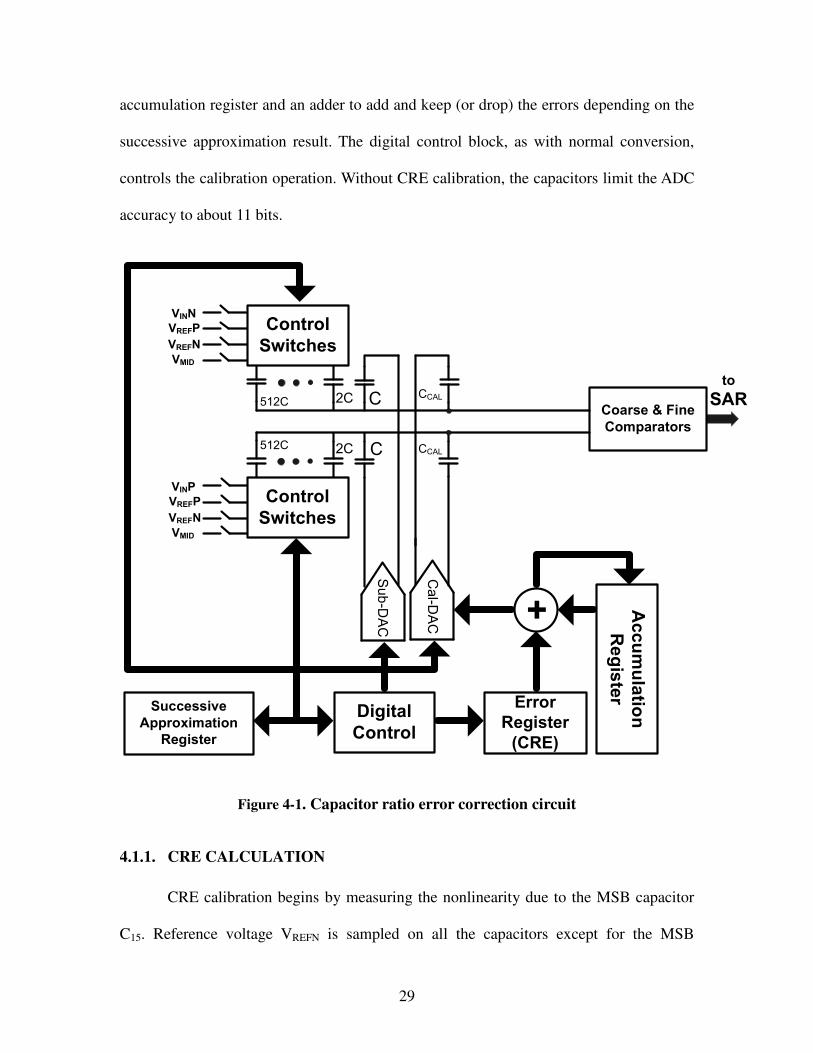
29
accumulation register and an adder to add and keep (or drop) the errors depending on the
successive approximation result. The digital control block, as with normal conversion,
controls the calibration operation. Without CRE calibration, the capacitors limit the ADC
accuracy to about 11 bits.
C
2C C
2C512C
512CCCAL
Control
Switches
Control
Switches
Successive
Approximation
Register
Digital
Control
VINN
VREFP
VREFN
VMID
VINP
VREFP
VREFN
VMID
Sub-DAC
Cal-DAC
Error
Register
(CRE)
Accumulation
Register
+
CCAL
to
SARCoarse & Fine
Comparators
Figure 4-1. Capacitor ratio error correction circuit
4.1.1. CRE CALCULATION
CRE calibration begins by measuring the nonlinearity due to the MSB capacitor
C15. Reference voltage VREFN is sampled on all the capacitors except for the MSB
30
capacitor being calibrated, which samples VREFP as shown in Figure 4-2 (a). Next,
sampled charge is redistributed by reversing the connection to the reference voltages as
shown in Figure 4-2 (b) [4].
(a)
(b)
Figure 4-2. CRE self-calibration process (a) CRE charging cycle. (b) Charge
redistribution to obtain error residual voltage
Without perfect capacitor matching, a residual voltage VXN corresponding to the
ratio error is reflected on the top plate, otherwise the top voltage remains unchanged. The
relation between the residual voltage and ratio error is given by equation (4.1).
ERRNRVN VV 2= (4.1)
31
The error voltage is then digitized using the cal-DAC and stored into memory.
The ratio errors of subsequent capacitors are calculated and stored digitally in memory in
the same way. The general relation between the residual voltages (VRVn’s) and the error
voltages (VERRn’s) is
.1...7,6,2
1
1
−=
−= ∑
+=
NnVVVN
ni
ERRiRVnERRn (4.2)
or digitally,
.1...7,6,2
1
1
−=
−= ∑
+=
NnDVDVDVN
ni
ERRiRVnERRn (4.3)
where DVERRn, DVRVn, and DVERRi stand for digitized ratio error, residual voltage, and
digitized ratio errors of previous MSB capacitors respectively. The capacitors in the
negative capacitor array are connected similarly, but to opposite voltage references.
4.1.2. CRE ERROR REMOVAL
During normal conversion the digital correction terms are added or subtracted
with the cal-DAC through CCAL as show in Figure 4-1. Digital errors corresponding to the
bit being tested is added to the correction term accumulated from previous bit correction
result. If the bit decision is 1, the added corrected digital word is stored in accumulation
register or else it is discarded. This operation effectively cancels the nonlinearity due to
capacitor mismatches and requires simple 2’s complement operation and digital memory
for implementation.
4.2. COMMON-MODE ERROR (CME) CALIBRATION
The CR ADC is implemented as a fully differential architecture with differential

32
inputs with fixed common-mode voltages. This greatly improves the common-mode
rejection capability of the ADC as well as cancels the linear voltage coefficient. However,
the parasitic capacitance at the top plate of the capacitor array limits the common-mode
rejection. These parasitic capacitances sample the input common-mode level during
sampling and contribute charges during the charge redistribution phase causing the
comparator offset to vary and the ADC linearity to depend on the common-mode signal.
A high common-mode rejection ratio (CMRR) comparator will be very insensitive to the
common-mode voltage, but device matching and other elements limits the comparator
CMRR to about 50dB [2]. Therefore, a self-calibration scheme is needed to cancel the
parasitic capacitors at the top plate of the capacitor array.
4.2.1. CME ADJUSTMENT SCHEME
Figure 4-3 presents the schematic of the CME adjustment circuit. It shows a
modified sampling scheme whereby variable capacitor CCME samples the voltage
difference GND-VREFP, where GND and VREFP are mid-rail and positive reference
voltage. Basically, CCME concurrently samples the difference voltage as the capacitor
array samples the input. The capacitors CP and CTOT represent the top-plate parasitic
capacitance and the total capacitance of the positive array respectively. CTRL represents
a set of switches that control the connection to the main capacitor array. The top plate of
CCME is connected to VREFN, the negative reference voltage, while its bottom plate is
connected to the comparator input after sampling [5]. This sampling scheme creates a
common-mode level to the comparator input given by
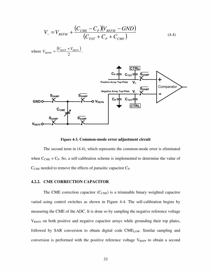
33
( )( )( )CMEPTOT
REFMPCMEREFM
CCC
GNDVCCVV
++
−−+=− (4.4)
where ( )
2
REFNREFPREFM
VVV
+= .
+
-ComparatorSSAMP
VREFN
VREFP
GNDCP CTOT
SSAMP
SSAMPSSAMP
SSAMP
Positive Array Top-Plate
Negative Array Top-Plate
CTOT SSAMPCP
CCME
V+
V-
CTRL
CTRL
Figure 4-3. Common-mode error adjustment circuit
The second term in (4.4), which represents the common-mode error is eliminated
when CCME = CP. So, a self-calibration scheme is implemented to determine the value of
CCME needed to remove the effects of parasitic capacitor CP.
4.2.2. CME CORRECTION CAPACITOR
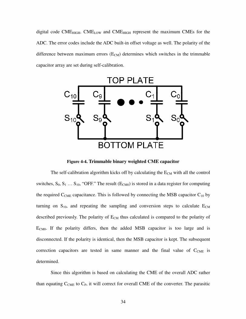
The CME correction capacitor (CCME) is a trimmable binary weighted capacitor
varied using control switches as shown in Figure 4-4. The self-calibration begins by
measuring the CME of the ADC. It is done so by sampling the negative reference voltage
VREFN on both positive and negative capacitor arrays while grounding their top plates,
followed by SAR conversion to obtain digital code CMELOW. Similar sampling and
conversion is performed with the positive reference voltage VREFP to obtain a second
34
digital code CMEHIGH. CMELOW and CMEHIGH represent the maximum CMEs for the
ADC. The error codes include the ADC built-in offset voltage as well. The polarity of the
difference between maximum errors (ECM) determines which switches in the trimmable
capacitor array are set during self-calibration.
Figure 4-4. Trimmable binary weighted CME capacitor
The self-calibration algorithm kicks off by calculating the ECM with all the control
switches, S0, S1 … S10, “OFF.” The result (ECM0) is stored in a data register for computing
the required CCME capacitance. This is followed by connecting the MSB capacitor C10 by
turning on S10, and repeating the sampling and conversion steps to calculate ECM
described previously. The polarity of ECM thus calculated is compared to the polarity of
ECM0. If the polarity differs, then the added MSB capacitor is too large and is
disconnected. If the polarity is identical, then the MSB capacitor is kept. The subsequent
correction capacitors are tested in same manner and the final value of CCME is
determined.
Since this algorithm is based on calculating the CME of the overall ADC rather
than equating CCME to CP, it will correct for overall CME of the converter. The parasitic
35
capacitances on the top plates of the positive and negative array are assumed to be the
same during the CME calibration. Any differences between them are calibrated using a
separate self-calibration algorithm.
4.3. OFFSET ERROR (OFT) CALIBRATION
The ADC consists of a built-in offset voltage arising from (a) the charge injection
from the switches that control the capacitor array and comparator offset cancellation and
(b) device mismatches in the comparator and input buffer. The OFT correction circuit
consists of a variable binary weighted capacitors COFTP and COFTN, similar to variable
CME capacitor, which couples a known signal to one of the top plate of the capacitor
array. Figure 4-5 shows the OFT correction circuit along with a parasitic capacitance CP
and total array capacitance CTOT. The connection to COFTP and COFTN in the positive and
the negative capacitor array is controlled by SOFTPOS and SOFTNEG, respectively.
Figure 4-5. Offset error correction circuit
36
The self-calibration algorithm begins by sampling and converting a zero-
differential signal with common mode level at( )
2
REFNREFPREFM
VVV
+= . In presence of no
offset error, the output code will be a zero (signifying mid-rail). However, presence of
any offset error necessitates an addition of correction capacitors to one of the top-plates
of the capacitor array. Depending on whether the output has a positive or a negative
offset, either COFTN or COFTP is connected to the respective top plate. The bottom plate of
the corresponding correction capacitor is connected to GND while sampling and to the
VREFP during conversion. The self-calibration algorithm runs the conversion and trims the
connected correction capacitor until a zero output is produced. The calculated trim
capacitor is applied during normal ADC conversion to cancel the offset error.
4.4. GAIN ERROR (GE) CALIBRATION
With CRE and CME already calibrated, the total capacitance of the negative and
positive array might not be equal. This gives rise to gain error (GE). Since GE varies with
process and ADC operating conditions, a self-calibration must be performed to eliminate
it. The gain of the ADC can be corrected by changing the amount of charge sampled onto
main capacitor arrays. This is done so by adding a trimmable binary weighted capacitor
on one of the capacitor array. Figure 4-6 shows the GE correction circuit. It shows binary
weighted GE adjustment capacitor arrays CGEP and CGEN, similar to the one used for
CME calibration, and control switches SGEPOS and SGENEG that are complementary in
nature. Depending on the result of the GE calibration algorithm, either CGEPOS or CGENEG
is turned “ON” to control the fraction of capacitance to adjust for GE. ∆CP represents the
37
extra parasitic capacitance on either the negative or the positive capacitor array.
Figure 4-6. Gain error correction circuit
The GE self-calibration begins by sampling a full-scale input, i.e. full reference
voltages and converting it. In absence of the GE, is should produce full-scale output.
However, if the result is small or saturated at maximum, then the GE adjustment
capacitor is added to the negative capacitor array or the positive capacitor array,
respectively. Identifying the smaller output code is obvious, but identifying whether the
gain saturated at maximum can be tricky. If the ADC produces full-scale output, then
MSB capacitor of the CGENEG is connected and the conversion is done again using full
reference voltages input. The MSB is kept if the output code is full-scale, otherwise is
discarded. The subsequent binary weighted capacitors are tested (kept or discarded) in
same manner. If the output is small, then CGEPOS is connected. The binary-weighted
capacitors are kept only if they produce smaller output code, otherwise are thrown out.
The correction capacitor remains connected during normal conversion to eliminate GE.
38
The bottom plates of the GE correction capacitors are connected to GND during sampling
and to VREFP during normal conversion, just like the OFT calibration.
CRE and CME calibration are two important calibrations for the ADC, as the
offset error and gain error can transcend from the previous sensor amplifier channel.
39
5.0. SIMULATION RESULTS
The low-power CR ADC is designed in a 0.25µm CMOS process. The ADC
consumes 4.23mW of power, including I/O, during low-noise high power operation from
a ± 1.5V supply. The verification of the performance of the ADC is discussed in this
section. The ADC components and the self-calibration process were verified separately at
first, then as a whole unit.
5.1. INPUT BUFFER
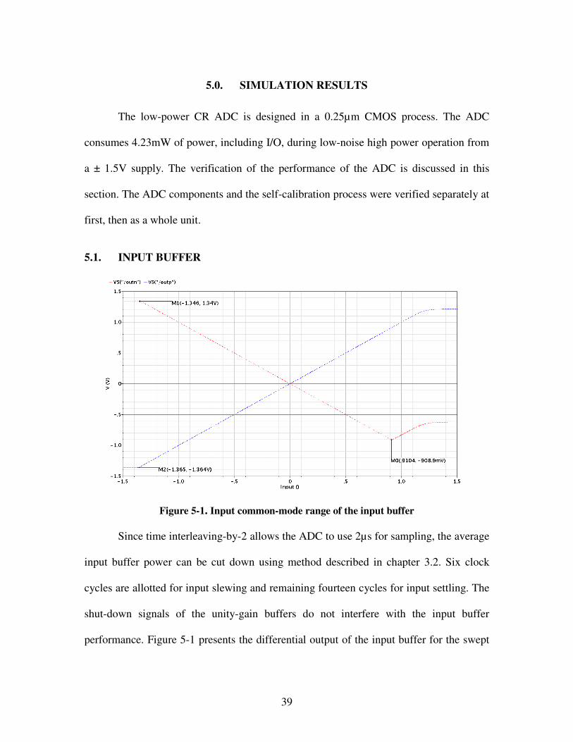
Figure 5-1. Input common-mode range of the input buffer
Since time interleaving-by-2 allows the ADC to use 2µs for sampling, the average
input buffer power can be cut down using method described in chapter 3.2. Six clock
cycles are allotted for input slewing and remaining fourteen cycles for input settling. The
shut-down signals of the unity-gain buffers do not interfere with the input buffer
performance. Figure 5-1 presents the differential output of the input buffer for the swept
40
input common-mode voltage and illustrates that the buffer is linear between input ranges
of -1.346 V and 0.91 V. Furthermore, the input buffer offset is measured at -191.8 µV.
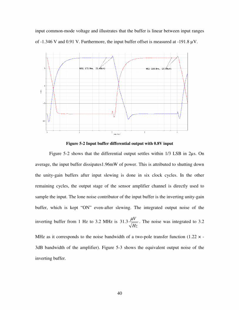
Figure 5-2 Input buffer differential output with 0.8V input
Figure 5-2 shows that the differential output settles within 1/3 LSB in 2µs. On
average, the input buffer dissipates1.96mW of power. This is attributed to shutting down
the unity-gain buffers after input slewing is done in six clock cycles. In the other
remaining cycles, the output stage of the sensor amplifier channel is directly used to
sample the input. The lone noise contributor of the input buffer is the inverting unity-gain
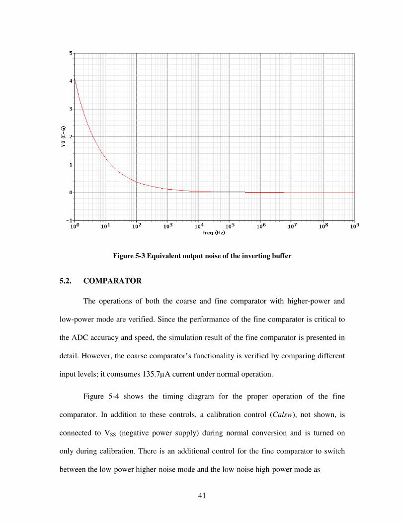
buffer, which is kept “ON” even-after slewing. The integrated output noise of the
inverting buffer from 1 Hz to 3.2 MHz is Hz
Vµ3.31 . The noise was integrated to 3.2
MHz as it corresponds to the noise bandwidth of a two-pole transfer function (1.22 × -
3dB bandwidth of the amplifier). Figure 5-3 shows the equivalent output noise of the
inverting buffer.
41
Figure 5-3 Equivalent output noise of the inverting buffer
5.2. COMPARATOR
The operations of both the coarse and fine comparator with higher-power and
low-power mode are verified. Since the performance of the fine comparator is critical to
the ADC accuracy and speed, the simulation result of the fine comparator is presented in
detail. However, the coarse comparator’s functionality is verified by comparing different
input levels; it comsumes 135.7µA current under normal operation.
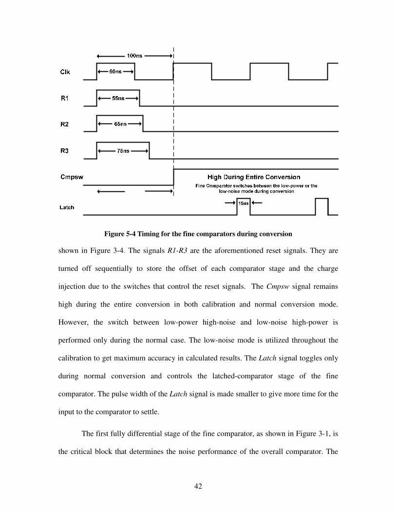
Figure 5-4 shows the timing diagram for the proper operation of the fine
comparator. In addition to these controls, a calibration control (Calsw), not shown, is
connected to VSS (negative power supply) during normal conversion and is turned on
only during calibration. There is an additional control for the fine comparator to switch
between the low-power higher-noise mode and the low-noise high-power mode as
42
Figure 5-4 Timing for the fine comparators during conversion
shown in Figure 3-4. The signals R1-R3 are the aforementioned reset signals. They are
turned off sequentially to store the offset of each comparator stage and the charge
injection due to the switches that control the reset signals. The Cmpsw signal remains
high during the entire conversion in both calibration and normal conversion mode.
However, the switch between low-power high-noise and low-noise high-power is
performed only during the normal case. The low-noise mode is utilized throughout the
calibration to get maximum accuracy in calculated results. The Latch signal toggles only
during normal conversion and controls the latched-comparator stage of the fine
comparator. The pulse width of the Latch signal is made smaller to give more time for the
input to the comparator to settle.
The first fully differential stage of the fine comparator, as shown in Figure 3-1, is
the critical block that determines the noise performance of the overall comparator. The
43
gain of the first stage during the low-noise mode is 34.5 dB, hence, the noise due to
subsequent stages is heavily suppressed, as their noise contributions are divided by the
gain of the first stage. Hence, the equivalent input noise contribution from the low-noise
differential stage can represent the noise due to the comparator and is presented in Figure
5-5.
Figure 5-5 Equivalent input noise of the high-power low-noise first stage fully differential
amplifier
The total input-referred noise for the low-noise differential stage when integrated
from 1 Hz to 100 MHz is Hz
Vµ4.17 while dissipating 591.74µA current. The noise
corresponds to 0.285 LSB of the ADC. The low-power mode has a gain of 29.15 dB,
input referred noise of Hz
Vµ7.48 and dissipates 89µA current. Furthermore, the fine
comparator is able to resolve up to 22.4µV of input difference, which is found by feeding
a negative and then positive ramp signal to the positive comparator input while grounding
the other input.
44
The low-power technique discussed in chapter 3.1.2. is verified by simulating the
comparator. Figure 5-6 presents the result. The simulation is done by giving two clock
cycles, for both the low-power and low-noise mode, to power-up and reset and
alternating the comparison cycle. Four comparisons are made by each mode.
Figure 5-6 Fine comparator output illustrating switch between the low-power and low-noise
mode
The waveforms represent low-noise mode control, low-power mode control,
cmpsw, and comparator output, followed by latch signal. Logic low cmpsw signal
signifies that the comparator is in reset phase and logic high level signifies comparison
phase. The low-power mode makes the first conversion followed by the reset and
comparison phases of the low-noise mode. Even though, the transition from the low-
power mode to low-noise mode is operating properly in fine comparator simulation, it has
not been implemented correctly in actual ADC conversion. The details need to be
analyzed for correct operation based on Table I.
45
5.3 CRE CALIBRATION
The CRE is the major player in limiting the linearity and resolution of the ADC.
The digital algorithm to calculate the CREs among the binary-weighted capacitors and
add them correctly during normal conversion is verified by introducing random ratio
mismatches to the first couple of MSBs of both the negative and positive capacitor array.
The errors are verified by adding them during the normal conversion of a known signal.
The ratio errors result in the wrong digital output. Adding the calculated CRE terms
should correct it.
Figure 5-7 (a) & (b) show the ADC result with capacitor-ratio mismatches put
randomly in the first three MSB capacitors. The uncalibrated ADC result is hex A669 for
an input of 300mV, the correct result being hex A667. The CREs calculated by the digital
algorithm are added through CCAL and correct result hex 6667 is produced for the same
input.
(a)
46
(b)
Figure 5-7 ADC conversion result showing CRE (a) Full conversion cycle. (b) Last 8 bits of
the converted result
Figure 5-8 Last 8 bits of the ADC result corrected by adding calculated CREs
Figure 5-8 shows the corrected ADC result. The calculated digital errors for the first
10 MSBs are hex EE, 00, 19, FC, FE, FF, FF, 00, 00, and 00 respectively. Large errors
are not expected in the ADC because of relative low mismatches among the metal-
insulator-metal capacitors (MIM-CAP) present in TSMC’s 0.25µm CMOS process. The
47
8-bit Cal-DAC should have adequate range to fix maximum CREs that may arise due to
fabrication introduced mismatches.
5.4. CME CALIBRATION
To test the algorithm for correcting the CME, 1pF and 1.05pF parasitic capacitors
are added to both the negative and positive capacitor array top-plates. By converting
zero-differential inputs with common-mode at VREFN and VREFP, respectively, the
maximum CME, ECM0, is calculated as a hex FFFD. The algorithm discussed in chapter
4.2 was not able to trim the CME capacitors to correct for the common-mode error. This
is either due to the error modeling problem or the algorithm itself is wrong. A better error
model, and possibly a new algorithm has to be used to correct for the CME. The
simulation showed no common-mode errors when the top plate parasitic capacitors are
made equal.
5.5. OFT CALIBRATION
The offset error present in the ADC is self-calibrated using the digital algorithm
attached in the Appendix VI. As mentioned earlier, mid-rail input signal (zero differential
input) is converted using the ADC, and if there is any offset error, the result will not
equal hex 8000. To test the algorithm a 300µV offset is introduced to the positive input of
the comparator. The resulted ADC conversion is hex 8004, inferring 4 LSB offset error.
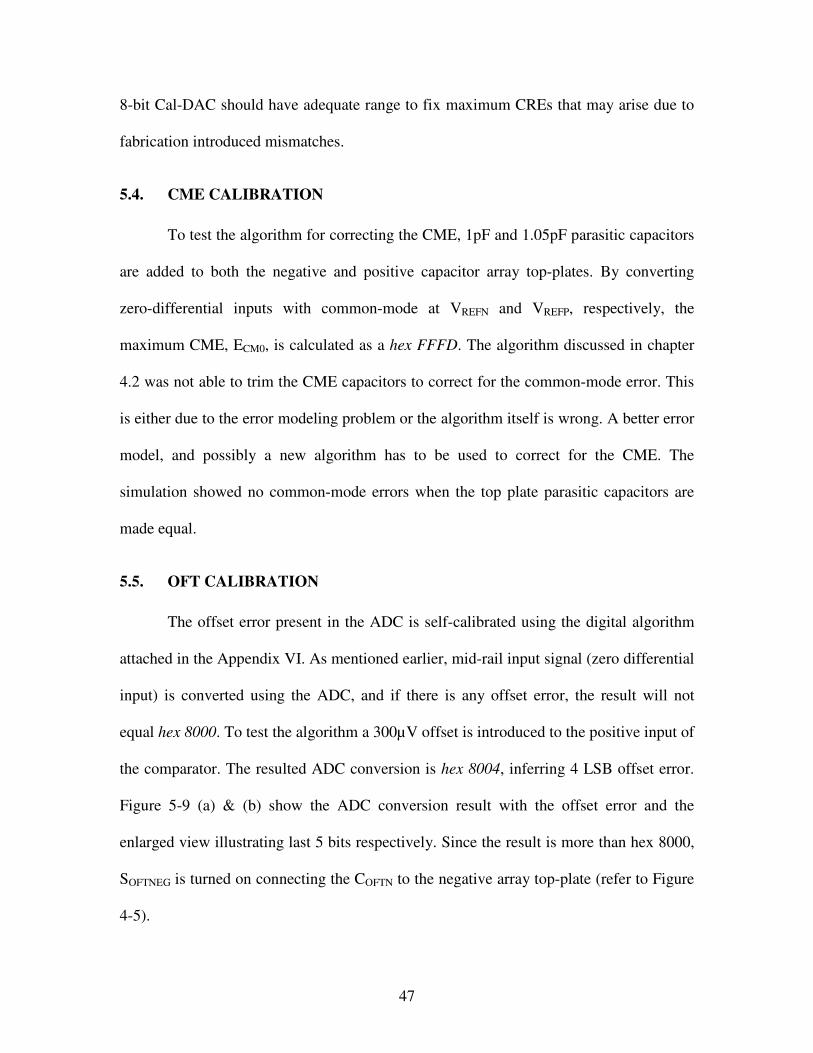
Figure 5-9 (a) & (b) show the ADC conversion result with the offset error and the
enlarged view illustrating last 5 bits respectively. Since the result is more than hex 8000,
SOFTNEG is turned on connecting the COFTN to the negative array top-plate (refer to Figure
4-5).
48
(a)
(b)
Figure 5-9 ADC conversion result showing offset error (a) Full conversion cycle. (b) Last 5
bits of the converted result
49
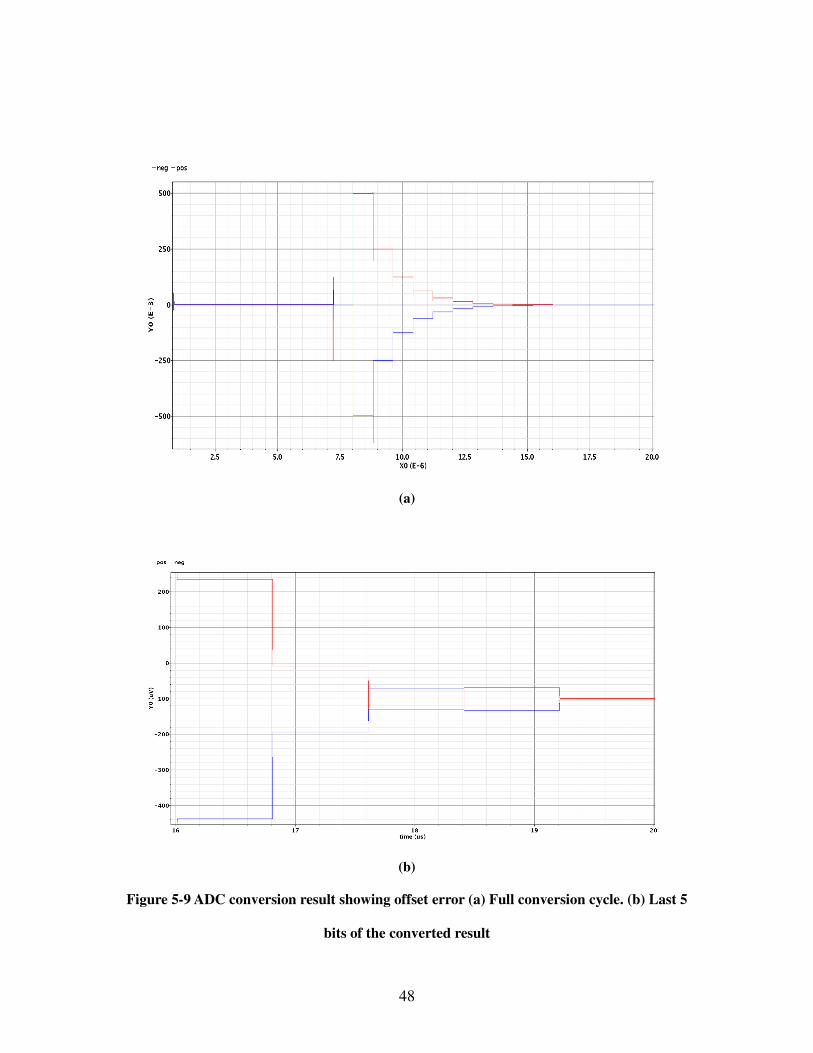
Figure 5-10 Enlarged view of the last 5 bits of the correct converted result with offset error
correction capacitor
The algorithm is used to trim the correction capacitor to hex 014 which is
equivalent to 20 LSBs or 15.625fF. Figure 5-10 shows the correct conversion result and
its zoomed in version, respectively. The algorithm was also tested for 300µV offset on
the negative input as well. It resulted in hex 7FFB and came up with hex 018 equivalent
to 22 LSB or 17.1875fF for the correction capacitor. This algorithm can correct the offset
error of the entire ADC.
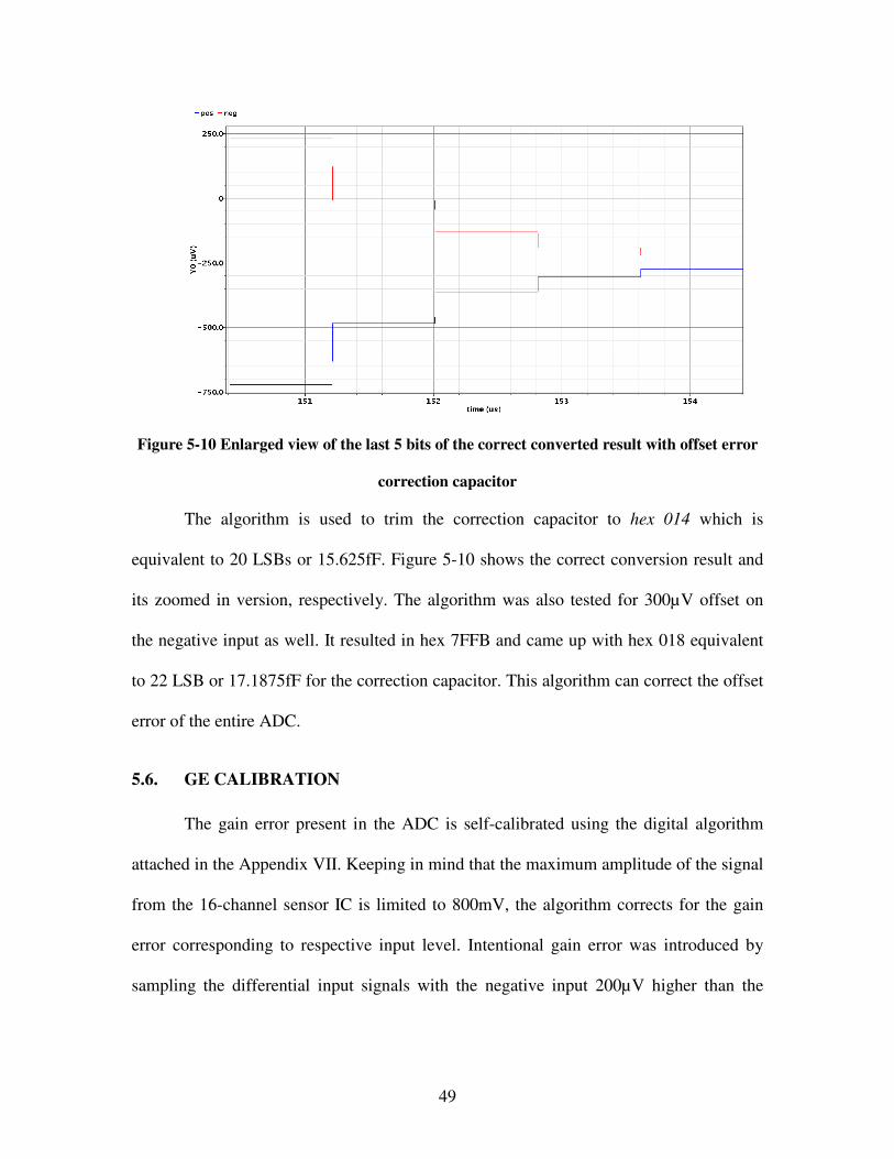
5.6. GE CALIBRATION
The gain error present in the ADC is self-calibrated using the digital algorithm
attached in the Appendix VII. Keeping in mind that the maximum amplitude of the signal
from the 16-channel sensor IC is limited to 800mV, the algorithm corrects for the gain
error corresponding to respective input level. Intentional gain error was introduced by
sampling the differential input signals with the negative input 200µV higher than the
50
positive input. This resulted in hex E669, which is 2 LSB larger than desired hex E667,
the correct digital code for 800mV input signal.
(a)
(b)
Figure 5-11 ADC conversion result showing a gain error (a) Full conversion cycle. (b) Last 5
bits of the converted result
51
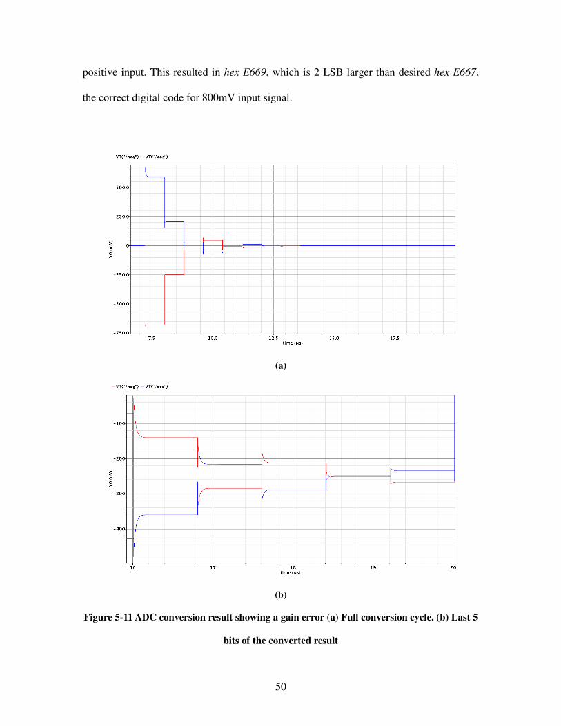
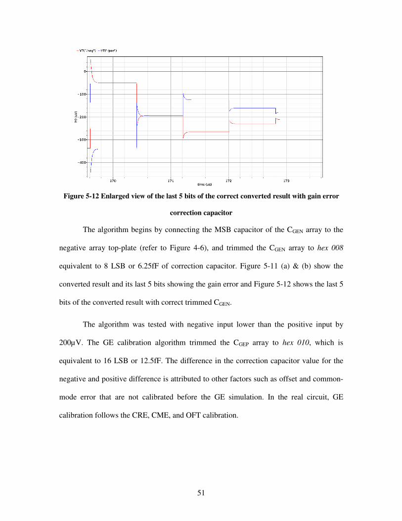
Figure 5-12 Enlarged view of the last 5 bits of the correct converted result with gain error
correction capacitor
The algorithm begins by connecting the MSB capacitor of the CGEN array to the
negative array top-plate (refer to Figure 4-6), and trimmed the CGEN array to hex 008
equivalent to 8 LSB or 6.25fF of correction capacitor. Figure 5-11 (a) & (b) show the
converted result and its last 5 bits showing the gain error and Figure 5-12 shows the last 5
bits of the converted result with correct trimmed CGEN.
The algorithm was tested with negative input lower than the positive input by
200µV. The GE calibration algorithm trimmed the CGEP array to hex 010, which is
equivalent to 16 LSB or 12.5fF. The difference in the correction capacitor value for the
negative and positive difference is attributed to other factors such as offset and common-
mode error that are not calibrated before the GE simulation. In the real circuit, GE
calibration follows the CRE, CME, and OFT calibration.
52
5.7. ADC PERFORMANCE
The performance of the 16-bit CR ADC is verified by measuring various
performance metrics, which are presented in this section.
5.7.1. NOISE
The noise of the ADC is calculated as a RMS sum of the noise contributions from
the fine comparator and kT/C noise due to sampling switches, as shown in equation (5.1).
( )2
,
22
, COMPn
PN
TOTn VC
kT
C
kTV +
+
= (5.1)
where, CN and CP represents the total capacitance of the negative and positive capacitor
array and Vn,COMP represents the total input-referred noise of the fine comparator.
The total noise of the ADC is given by
( )Hz
VV TOTn
µ64.214.17
1050
10142.4
1050
10142.4 2
2
12
212
12
21
, =+
×
×+
×
×=
−
−
−
−
As mentioned earlier, the sizes of the capacitor arrays are increased to lower the
kT/C noise and fine comparator first stage is made lower noise and relatively high gain to
suppress the noise from the subsequent stages.
5.7.2. POWER
The overall power of the ADC is dominated by the comparators and the input
buffer. The fine comparator dissipates 762.3µW and 2.27mW under the low-power mode
and the low-noise high-power mode, respectively, while the input buffer burns an average
53
of 1.96mW power. Currently, the switching between the low-power and low-noise mode
is not operating correctly with shut-down signals. However, if the technique is
operational, then the average power consumed by the ADC is equivalent to power
consumed by the input buffer, the coarse comparator, and the low-power and the low-
noise mode of the fine comparator, for the time each blocks are kept on. In that case, the
average power of the ADC including the input buffer is given by equation (5.2).
×+
×+
×+
×=
TOT
ON
LN
TOT
ON
LP
TOT
ON
TOT
ON
DT
TFine
T
TFine
T
TCoarse
T
TBufferP 4321 (5.2)
where, buffer, coarse, fineLP and fineLN represents the average power dissipated by the
input buffer, coarse comparator, low-power mode of the fine comparator, and the low-
noise mode of the fine comparator, respectively. TON represents the total number of clock
cycles each component is turned on, and TTOT represents the total clock cycles. The
average power dissipation of the ADC, in such case, will be
mWmmmPD 42.320
416.1
20
627.2
20
91.3.762
20
101.40796.1 =
×+
×+
×+
×+= µµ
The average power dissipation is still high and can be lowered further by
decreasing the shut-down current. A shut-down signal is not currently implemented in the
second stage of the fine comparator, which consumes 109.9µA. Adding the shut-down
feature, in addition to lowering the overall shut-down current in each stage will help curb
higher power dissipation.
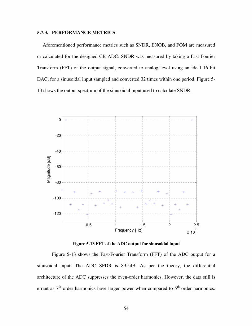
54
5.7.3. PERFORMANCE METRICS
Aforementioned performance metrics such as SNDR, ENOB, and FOM are measured
or calculated for the designed CR ADC. SNDR was measured by taking a Fast-Fourier
Transform (FFT) of the output signal, converted to analog level using an ideal 16 bit
DAC, for a sinusoidal input sampled and converted 32 times within one period. Figure 5-
13 shows the output spectrum of the sinusoidal input used to calculate SNDR.
0.5 1 1.5 2 2.5
x 105
-120
-100
-80
-60
-40
-20
0
Frequency [Hz]
Magnitude [
dB
]
Figure 5-13 FFT of the ADC output for sinusoidal input
Figure 5-13 shows the Fast-Fourier Transform (FFT) of the ADC output for a
sinusoidal input. The ADC SFDR is 89.5dB. As per the theory, the differential
architecture of the ADC suppresses the even-order harmonics. However, the data still is
errant as 7th
order harmonics have larger power when compared to 5th
order harmonics.
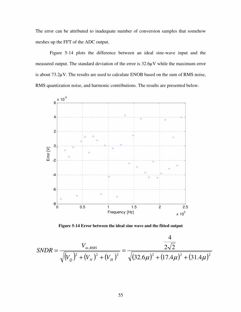
55
The error can be attributed to inadequate number of conversion samples that somehow
meshes up the FFT of the ADC output.
Figure 5-14 plots the difference between an ideal sine-wave input and the
measured output. The standard deviation of the error is 32.6µV while the maximum error
is about 73.2µV. The results are used to calculate ENOB based on the sum of RMS noise,
RMS quantization noise, and harmonic contributions. The results are presented below.
0 0.5 1 1.5 2 2.5
x 105
-8
-6
-4
-2
0
2
4
6x 10
-5
Frequency [Hz]
Err
or
[V]
Figure 5-14 Error between the ideal sine wave and the fitted output
( ) ( ) ( ) ( ) ( ) ( )222222
,
4.314.176.32
22
4
µµµ ++=
++=
HNQ
RMSin
VVV
VSNDR

56
( )Bits
SNDRENOB dB 49.14
02.6
76.1102.28log20
02.6
76.1 3
=−××
=−
=
StepConvfJm
BW
PFOM
ENOB
D ./3.1161050022
1.40727.2
22 349.14=
×××
+=
××=
µ
The power of the ADC can be reduced further after implementing the low-power
technique by effectively switching between the low-power and low-noise mode in the
fine comparator and shutting-down the system not in use. The optimistic FOM factor
with all these factors implemented is excellent 63.4 fJ / conversion step. The result will
be phenomenal when compared to existing state-of-the-art ADCs.
57
6.0. CONCLUSION
A self-calibrating low power 16-bit 500 KSps CR ADC was successfully
designed and simulated in TSMC 0.25 µm CMOS process. Results show that the
capacitor ratio errors, common-mode error, offset error and gain error were successfully
calculated and corrected. The results verified the functionality of the 16-bit ADC with a
power consumption of 4.23mW including the input buffer. The input buffer dissipates
1.96mW of power. The ADC has an input range of ± 1V and SNDR of 89.01dB, which
equates to ENOB of 14.49 bits. The SFDR is 89.5dB. The FOM factor for the ADC is
116.3 fJ/conversion step which compares well with existing state-of-the-art ADCs. The
results show erroneous FFT plot of the ADC output for a sinusoidal input with the 7th
harmonic power being larger than 5th
harmonic power. The anomaly if located and fixed,
will improve the ADC resolution to higher than 15-bits and improve the FOM factor
considerably.
The time interleaving-by-2 along with switching between the coarse and the fine
comparator with low-power and higher-power mode effectively reduced the ADC power
while maintaining speed and accuracy.
The 16-bit ADC was designed for the VCAAP at Washington State University to
acquire and digitize the neural signals of small rodents during their sleep cycle. Together
with 16-channel sensor IC, also designed at WSU [2], and wireless telemetry system, the
sensor IC chip will be a state-of-the-art sensor IC with excellent speed, accuracy, and
power performance.

58
6.1. FUTURE WORKS
The current design of the 16-bit CR ADC can be modified to further suit the
neuro-sensory application. The fact that the sensor IC chips require smaller die area and
low power consumption begets the need of further research and methods to accomplish
them.
One direction that improves the design is by designing programmable resolution
ADC. The ADC can operate in smaller 12-bits or higher 15-bit resolution mode. This
makes sense as the neural signals from the animals are amplitude-varying. The lower
resolution ADC can be used to digitize the signals with larger amplitudes while higher
resolution can digitize smaller amplitudes.. The current design can swiftly be redesigned
to add resolution programmability because of relatively simple digital control logic. The
programmability offers a low-power 12-bit ADC resolution mode and higher-power 15-
bit mode which will still be lower power when compared to the current design. The idea
of having resolution smaller than 16-bit translates to relaxing various design requirements
such as, large current consumption, large device geometry and large capacitors put
together to reduce noise to achieve 16-bit resolution.
The power supply of ± 1.5V can be reduced to ± 1.2V. Even though this reduces
the dynamic range of the ADC, the power can be lowered and 2V thick oxide 0.25 µm
process MOS devices can be implemented. The current design uses intrinsic 3V thick
oxide 0.25 µm process MOS devices to handle ± 1.5V power supply. The 2V MOS
devices are faster and have lower noise when compared to the 3V device, because of
higher fT and larger COX. Furthermore, the lowering of power supply is necessary because
of the improvement in 16-channel sensor IC chip performance when designed in ± 1.2V
59
power supply.
Another path that the current design can take is implementing individual ADC for
each of the 16 amplifier channels in the sensor IC chip. This effectively removes the 16:1
multiplexer that selects one of the 16 channel outputs. The multiplexer in the current
sensor IC design dissipates a large amount of power. In essence, this design will seek to
trade area for power.
The performance of the current design should be verified by characterizing the
fabricated chip. Furthermore, the low-power technique of switching between the low-
power and low-noise mode of the fine comparator should be completed as well. Only
then can the possibility of improving the performance be realized. However, if
successfully implemented, the new modified ADC will be beneficial to various clinical
and animal research areas.
60
BIBLIOGRAPHY
1. T. Akin, et al, A wireless implantable multichannel digital neural recording
system for a micromachined sieve electrode,” IEEE J. of Solid-State Circuits,
vol. 33, Jan. 1998.
2. H Guo, “ A low power low-noise high accuracy sensor IC,” doctoral
dissertation, Dept. Electrical Engineering and Computer Science, Washington
State University, Pullman, Washington, the USA, 2006.
3. H.S. Lee, et al, “A self-calibration 15-bit CMOS A/D converter,” IEEE J. Solid-
State Circuits, Vol. SC-19, pp. 813-819, Dec. 1984.
4. H.S. Lee, et al, “Self-Calibration Technique for A/D Converters,” IEEE Trans.
on Circuits and Systems, Vol. Cad-30, No. 3, pp. 188-190, March 1983.
5. K. S. Tan, et al, “Error correction techniques for high-performance differential
A/D converters,” IEEE J. Solid-State Circuits, Vol. 25 , no. 6 , pp. 1318 –
1327, Dec. 1990.
6. R.K. Hester et al., “Fully differential ADC with rail-to-rail common-mode range
and nonlinear capacitor compensation,” IEEE J. Solid-State Circuits, vol. 25 no.
1, pp. 173-183, Feb. 1990.
7. J.L. McCreary, et al., “All-MOS charge redistribution A/D conversion
techniques ---Part I,” IEEE J. Solid-State Circuits, Vol. SC-10, pp. 371-379,
Dec. 1975.
8. G.M.Yin, et al, ”A high-speed CMOS comparator with 8-b resolution,” IEEE J.
Solid-State Circuits, Vol. 27 , no. 2, pp. 208 – 211, Feb. 1992.

61
9. B. Razavi, Principles of Data Conversion System Design, Piscataway: IEEE
Press,1995.
10. T.L. Tewksbury, et al, "The effects of oxide traps on the large-signal transient
response of analog MOS circuits," IEEE J. Solid-State Circuits, Vol. 24 , no. 2 ,
pp. 542 – 544, April 1989.
11. D. Johns, and K. Martin, Analog Integrated Circuit Design, Toronto: John
Wiley& Sons, Inc, 1997.
12. B. Razavi, Design of Analog CMOS Integrated Circuits, New York: McGraw-
Hill, 2001.
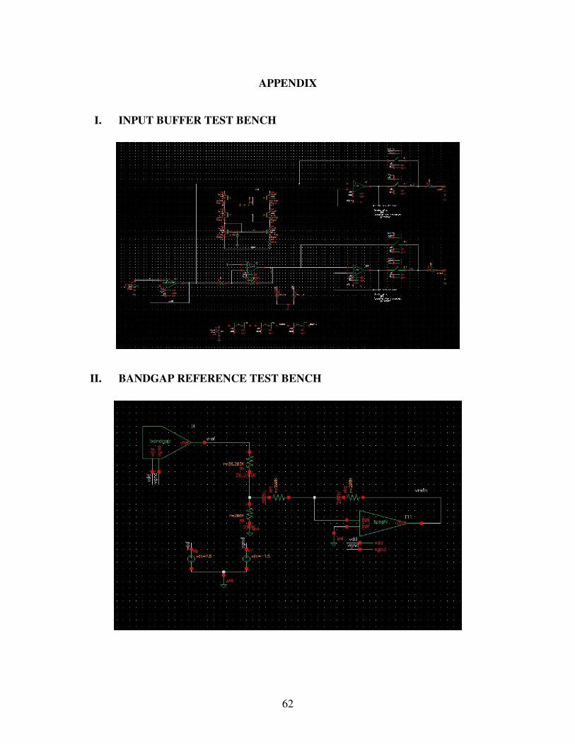
62
APPENDIX
I. INPUT BUFFER TEST BENCH
II. BANDGAP REFERENCE TEST BENCH
63
III. ADC TEST BENCH
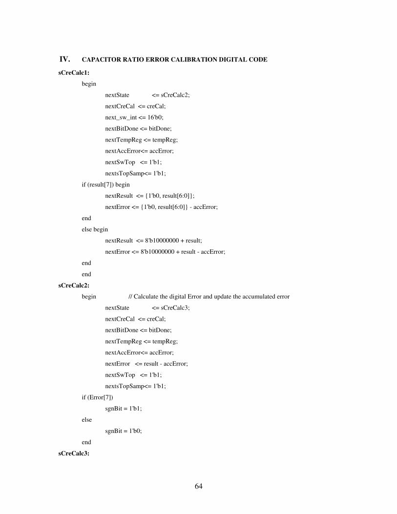
64
IV. CAPACITOR RATIO ERROR CALIBRATION DIGITAL CODE
sCreCalc1:
begin
nextState <= sCreCalc2;
nextCreCal <= creCal;
next_sw_int <= 16'b0;
nextBitDone <= bitDone;
nextTempReg <= tempReg;
nextAccError<= accError;
nextSwTop <= 1'b1;
nextsTopSamp<= 1'b1;
if (result[7]) begin
nextResult <= {1'b0, result[6:0]};
nextError <= {1'b0, result[6:0]} - accError;
end
else begin
nextResult <= 8'b10000000 + result;
nextError <= 8'b10000000 + result - accError;
end
end
sCreCalc2:
begin // Calculate the digital Error and update the accumulated error
nextState <= sCreCalc3;
nextCreCal <= creCal;
nextBitDone <= bitDone;
nextTempReg <= tempReg;
nextAccError<= accError;
nextError <= result - accError;
nextSwTop <= 1'b1;
nextsTopSamp<= 1'b1;
if (Error[7])
sgnBit = 1'b1;
else
sgnBit = 1'b0;
end
sCreCalc3:
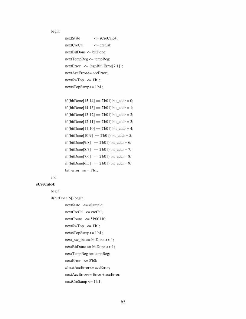
65
begin
nextState <= sCreCalc4;
nextCreCal <= creCal;
nextBitDone <= bitDone;
nextTempReg <= tempReg;
nextError <= {sgnBit, Error[7:1]};
nextAccError<= accError;
nextSwTop <= 1'b1;
nextsTopSamp<= 1'b1;
if (bitDone[15:14] == 2'b01) bit_addr = 0;
if (bitDone[14:13] == 2'b01) bit_addr = 1;
if (bitDone[13:12] == 2'b01) bit_addr = 2;
if (bitDone[12:11] == 2'b01) bit_addr = 3;
if (bitDone[11:10] == 2'b01) bit_addr = 4;
if (bitDone[10:9] == 2'b01) bit_addr = 5;
if (bitDone[9:8] == 2'b01) bit_addr = 6;
if (bitDone[8:7] == 2'b01) bit_addr = 7;
if (bitDone[7:6] == 2'b01) bit_addr = 8;
if (bitDone[6:5] == 2'b01) bit_addr = 9;
bit_error_we = 1'b1;
end
sCreCalc4:
begin
if(bitDone[6]) begin
nextState <= sSample;
nextCreCal <= creCal;
nextCount <= 5'b00110;
nextSwTop <= 1'b1;
nextsTopSamp<= 1'b1;
next_sw_int <= bitDone >> 1;
nextBitDone <= bitDone >> 1;
nextTempReg <= tempReg;
nextError <= 8'b0;
//nextAccError<= accError;
nextAccError<= Error + accError;
nextCreSamp <= 1'b1;
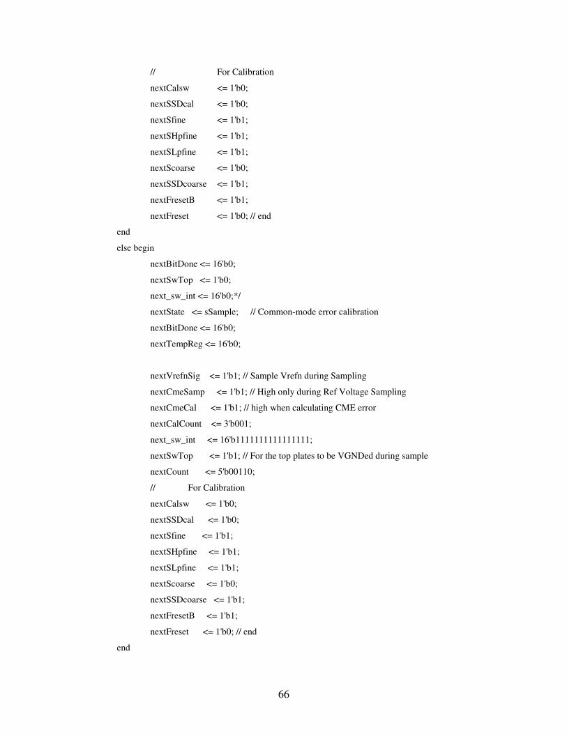
66
// For Calibration
nextCalsw <= 1'b0;
nextSSDcal <= 1'b0;
nextSfine <= 1'b1;
nextSHpfine <= 1'b1;
nextSLpfine <= 1'b1;
nextScoarse <= 1'b0;
nextSSDcoarse <= 1'b1;
nextFresetB <= 1'b1;
nextFreset <= 1'b0; // end
end
else begin
nextBitDone <= 16'b0;
nextSwTop <= 1'b0;
next_sw_int <= 16'b0;*/
nextState <= sSample; // Common-mode error calibration
nextBitDone <= 16'b0;
nextTempReg <= 16'b0;
nextVrefnSig <= 1'b1; // Sample Vrefn during Sampling
nextCmeSamp <= 1'b1; // High only during Ref Voltage Sampling
nextCmeCal <= 1'b1; // high when calculating CME error
nextCalCount <= 3'b001;
next_sw_int <= 16'b1111111111111111;
nextSwTop <= 1'b1; // For the top plates to be VGNDed during sample
nextCount <= 5'b00110;
// For Calibration
nextCalsw <= 1'b0;
nextSSDcal <= 1'b0;
nextSfine <= 1'b1;
nextSHpfine <= 1'b1;
nextSLpfine <= 1'b1;
nextScoarse <= 1'b0;
nextSSDcoarse <= 1'b1;
nextFresetB <= 1'b1;
nextFreset <= 1'b0; // end
end

67
end
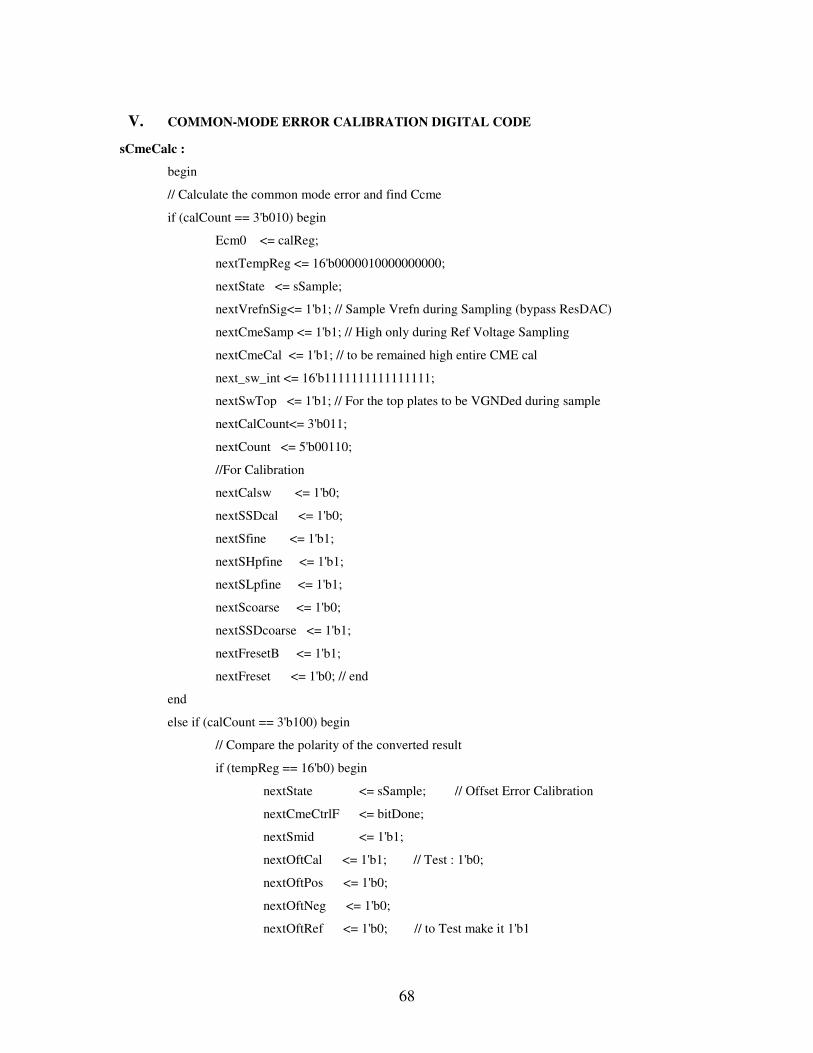
68
V. COMMON-MODE ERROR CALIBRATION DIGITAL CODE
sCmeCalc :
begin
// Calculate the common mode error and find Ccme
if (calCount == 3'b010) begin
Ecm0 <= calReg;
nextTempReg <= 16'b0000010000000000;
nextState <= sSample;
nextVrefnSig<= 1'b1; // Sample Vrefn during Sampling (bypass ResDAC)
nextCmeSamp <= 1'b1; // High only during Ref Voltage Sampling
nextCmeCal <= 1'b1; // to be remained high entire CME cal
next_sw_int <= 16'b1111111111111111;
nextSwTop <= 1'b1; // For the top plates to be VGNDed during sample
nextCalCount<= 3'b011;
nextCount <= 5'b00110;
//For Calibration
nextCalsw <= 1'b0;
nextSSDcal <= 1'b0;
nextSfine <= 1'b1;
nextSHpfine <= 1'b1;
nextSLpfine <= 1'b1;
nextScoarse <= 1'b0;
nextSSDcoarse <= 1'b1;
nextFresetB <= 1'b1;
nextFreset <= 1'b0; // end
end
else if (calCount == 3'b100) begin
// Compare the polarity of the converted result
if (tempReg == 16'b0) begin
nextState <= sSample; // Offset Error Calibration
nextCmeCtrlF <= bitDone;
nextSmid <= 1'b1;
nextOftCal <= 1'b1; // Test : 1'b0;
nextOftPos <= 1'b0;
nextOftNeg <= 1'b0;
nextOftRef <= 1'b0; // to Test make it 1'b1
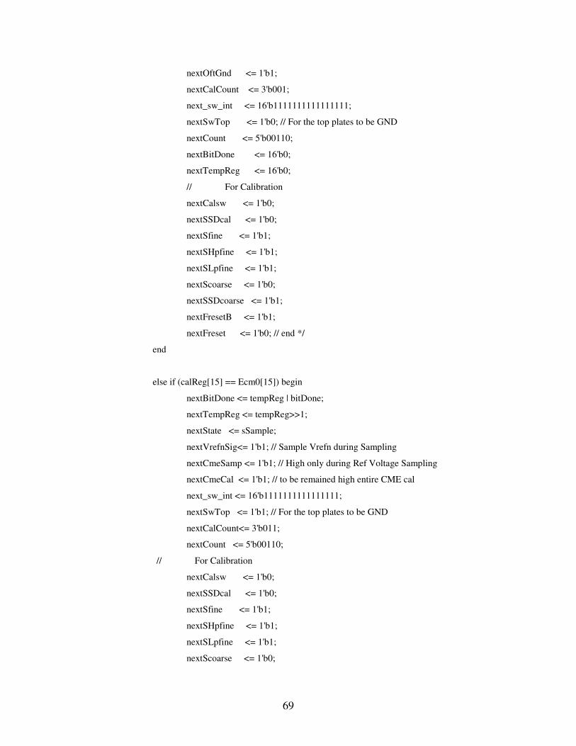
69
nextOftGnd <= 1'b1;
nextCalCount <= 3'b001;
next_sw_int <= 16'b1111111111111111;
nextSwTop <= 1'b0; // For the top plates to be GND
nextCount <= 5'b00110;
nextBitDone <= 16'b0;
nextTempReg <= 16'b0;
// For Calibration
nextCalsw <= 1'b0;
nextSSDcal <= 1'b0;
nextSfine <= 1'b1;
nextSHpfine <= 1'b1;
nextSLpfine <= 1'b1;
nextScoarse <= 1'b0;
nextSSDcoarse <= 1'b1;
nextFresetB <= 1'b1;
nextFreset <= 1'b0; // end */
end
else if (calReg[15] == Ecm0[15]) begin
nextBitDone <= tempReg | bitDone;
nextTempReg <= tempReg>>1;
nextState <= sSample;
nextVrefnSig<= 1'b1; // Sample Vrefn during Sampling
nextCmeSamp <= 1'b1; // High only during Ref Voltage Sampling
nextCmeCal <= 1'b1; // to be remained high entire CME cal
next_sw_int <= 16'b1111111111111111;
nextSwTop <= 1'b1; // For the top plates to be GND
nextCalCount<= 3'b011;
nextCount <= 5'b00110;
// For Calibration
nextCalsw <= 1'b0;
nextSSDcal <= 1'b0;
nextSfine <= 1'b1;
nextSHpfine <= 1'b1;
nextSLpfine <= 1'b1;
nextScoarse <= 1'b0;
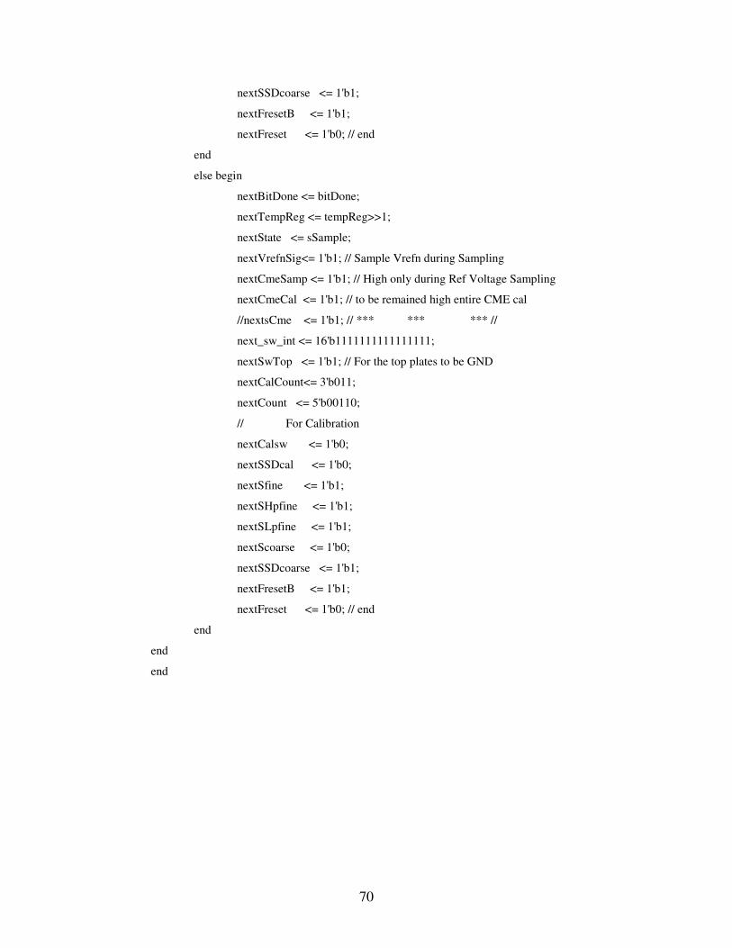
70
nextSSDcoarse <= 1'b1;
nextFresetB <= 1'b1;
nextFreset <= 1'b0; // end
end
else begin
nextBitDone <= bitDone;
nextTempReg <= tempReg>>1;
nextState <= sSample;
nextVrefnSig<= 1'b1; // Sample Vrefn during Sampling
nextCmeSamp <= 1'b1; // High only during Ref Voltage Sampling
nextCmeCal <= 1'b1; // to be remained high entire CME cal
//nextsCme <= 1'b1; // *** *** *** //
next_sw_int <= 16'b1111111111111111;
nextSwTop <= 1'b1; // For the top plates to be GND
nextCalCount<= 3'b011;
nextCount <= 5'b00110;
// For Calibration
nextCalsw <= 1'b0;
nextSSDcal <= 1'b0;
nextSfine <= 1'b1;
nextSHpfine <= 1'b1;
nextSLpfine <= 1'b1;
nextScoarse <= 1'b0;
nextSSDcoarse <= 1'b1;
nextFresetB <= 1'b1;
nextFreset <= 1'b0; // end
end
end
end
71
VI. OFFSET ERROR CALIBRATION DIGITAL CODE
sOftCalc:
begin
if (calCount == 3'b001) begin
if (result > 16'b1000000000000000) begin
nextOftNeg <= 1'b1;
nextOftCal <= oftCal;
nextOftRef <= 1'b1;
nextOftGnd <= 1'b0;
nextTempReg <= 16'b0000000100000000;
nextState <= sSample;
nextSwTop <= 1'b1;
nextSmid <= 1'b1;
next_sw_int <= 16'b1111111111111111;
nextCount <= 5'b00110;
nextCalCount <= 3'b0;
// For Calibration
nextCalsw <= 1'b0;
nextSSDcal <= 1'b0;
nextSfine <= 1'b1;
nextSHpfine <= 1'b1;
nextSLpfine <= 1'b1;
nextScoarse <= 1'b0;
nextSSDcoarse <= 1'b1;
nextFresetB <= 1'b1;
nextFreset <= 1'b0; // end
end
else if (result < 16'b1000000000000000) begin
nextOftPos <= 1'b1;
nextOftCal <= oftCal;
nextOftRef <= 1'b1;
nextOftGnd <= 1'b0;
nextTempReg <= 16'b0000000100000000;
nextState <= sSample;
nextSwTop <= 1'b1;
nextSmid <= 1'b1;
72
next_sw_int <= 16'b1111111111111111;
nextCount <= 5'b00110;
nextCalCount <= 3'b0;
// For Calibration
nextCalsw <= 1'b0;
nextSSDcal <= 1'b0;
nextSfine <= 1'b1;
nextSHpfine <= 1'b1;
nextSLpfine <= 1'b1;
nextScoarse <= 1'b0;
nextSSDcoarse <= 1'b1;
nextFresetB <= 1'b1;
nextFreset <= 1'b0; // end
end
else nextState <= sDoNot;
end
else begin
if (oftNeg) begin
if (result < 16'b1000000000000000) begin
nextBitDone <= bitDone;
nextOftCal <= oftCal;
nextOftRef <= 1'b1;
nextOftGnd <= 1'b0;
nextTempReg <= tempReg>>1;
nextState <= sSample;
nextSwTop <= 1'b1;
nextSmid <= 1'b1;
next_sw_int <= 16'b1111111111111111;
nextCount <= 5'b00110;
// For Calibration
nextCalsw <= 1'b0;
nextSSDcal <= 1'b0;
nextSfine <= 1'b1;
nextSHpfine <= 1'b1;
nextSLpfine <= 1'b1;
nextScoarse <= 1'b0;
nextSSDcoarse <= 1'b1;
73
nextFresetB <= 1'b1;
nextFreset <= 1'b0; // end
end
else if (result > 16'b1000000000000000) begin
nextBitDone <= (bitDone | tempReg);
nextOftCal <= oftCal;
nextOftRef <= 1'b1;
nextOftGnd <= 1'b0;
nextTempReg <= tempReg>>1;
nextState <= sSample;
nextSwTop <= 1'b1;
nextSmid <= 1'b1;
next_sw_int <= 16'b1111111111111111;
nextCount <= 5'b0110;
// For Calibration
nextCalsw <= 1'b0;
nextSSDcal <= 1'b0;
nextSfine <= 1'b1;
nextSHpfine <= 1'b1;
nextSLpfine <= 1'b1;
nextScoarse <= 1'b0;
nextSSDcoarse <= 1'b1;
nextFresetB <= 1'b1;
nextFreset <= 1'b0; // end
end
else begin
nextState <= sDoNot;
nextOftCtrlF <= (bitDone | tempReg);
end
end
else if(oftPos) begin
if (result > 16'b1000000000000000) begin
nextBitDone <= bitDone;
nextOftCal <= oftCal;
nextOftRef <= 1'b1;
nextOftGnd <= 1'b0;
nextTempReg <= tempReg>>1;
74
nextState <= sSample;
nextSwTop <= 1'b1;
nextsTopSamp<= 1'b1;
nextSmid <= 1'b1;
next_sw_int <= 16'b1111111111111111;
nextCount <= 5'b00110;
// For Calibration
nextCalsw <= 1'b0;
nextSSDcal <= 1'b0;
nextSfine <= 1'b1;
nextSHpfine <= 1'b1;
nextSLpfine <= 1'b1;
nextScoarse <= 1'b0;
nextSSDcoarse <= 1'b1;
nextFresetB <= 1'b1;
nextFreset <= 1'b0; // end
end
else if (result < 16'b1000000000000000) begin
nextBitDone <= (bitDone | tempReg);
nextOftCal <= oftCal;
nextOftRef <= 1'b1;
nextOftGnd <= 1'b0;
nextTempReg <= tempReg>>1;
nextState <= sSample;
nextSwTop <= 1'b1;
nextsTopSamp<= 1'b1;
nextSmid <= 1'b1;
next_sw_int <= 16'b1111111111111111;
nextCount <= 5'b00110;
// For Calibration
nextCalsw <= 1'b0;
nextSSDcal <= 1'b0;
nextSfine <= 1'b1;
nextSHpfine <= 1'b1;
nextSLpfine <= 1'b1;
nextScoarse <= 1'b0;
nextSSDcoarse <= 1'b1;
75
nextFresetB <= 1'b1;
nextFreset <= 1'b0; // end
end
else begin
nextState <= sDoNot;
nextOftCtrlF <= (bitDone | tempReg);
end
end
//else nextState <= sDoNot;
end
end
76
VII. GAIN ERROR CALIBRATION DIGITAL CODE
sCgeCalc:
begin
if (calCount == 3'b001) begin
if (result > 16'b1110_0110_0110_0111) begin
nextCgePos <= 1'b1;
nextCgeCal <= cgeCal;
nextTempReg <= 16'b0000_0100_0000_0000;
nextBitDone <= 16'b0;
nextState <= sSample;
nextSwTop <= 1'b1;
nextCgeSamp <= 1'b1;
next_sw_int <= 16'b1111_1111_1111_1111;
nextCount <= 5'b00110;
nextCalCount <= 3'b0;
// For Calibration
nextCalsw <= 1'b0;
nextSSDcal <= 1'b0;
nextSfine <= 1'b1;
nextSHpfine <= 1'b1;
nextSLpfine <= 1'b1;
nextScoarse <= 1'b0;
nextSSDcoarse <= 1'b1;
nextFresetB <= 1'b1;
nextFreset <= 1'b0; // end
end
else if (result < 16'b1110_0110_0110_0111) begin
nextCgeNeg <= 1'b1;
nextCgeCal <= cgeCal;
nextTempReg <= 16'b0000_0100_0000_0000;
nextBitDone <= 16'b0;
nextState <= sSample;
nextSwTop <= 1'b1;
nextCgeSamp <= 1'b1;
next_sw_int <= 16'b1111_1111_1111_1111;
nextCount <= 5'b00110;
77
nextCalCount <= 3'b0;
// For Calibration
nextCalsw <= 1'b0;
nextSSDcal <= 1'b0;
nextSfine <= 1'b1;
nextSHpfine <= 1'b1;
nextSLpfine <= 1'b1;
nextScoarse <= 1'b0;
nextSSDcoarse <= 1'b1;
nextFresetB <= 1'b1;
nextFreset <= 1'b0; // end
end
else nextState <= sDoNot;
end
else begin
if (tempReg == 16'b0) begin
nextState <= sDoNot;
if (result < 16'b1110_0110_0110_0111) begin
nextCgeCtrlF <= (bitDone | tempReg) + 2'b01;
end
else nextCgeCtrlF <= (bitDone | tempReg) + 1'b1;
end
else if (cgeNeg) begin
if (result > 16'b1110_0110_0110_0111) begin
nextBitDone <= bitDone;
nextCgeCal <= cgeCal;
nextTempReg <= tempReg>>1;
nextState <= sSample;
nextSwTop <= 1'b1;
nextCgeSamp <= 1'b1;
next_sw_int <= 16'b1111111111111111;
nextCount <= 5'b0110;
// For Calibration
nextCalsw <= 1'b0;
nextSSDcal <= 1'b0;
nextSfine <= 1'b1;
nextSHpfine <= 1'b1;
78
nextSLpfine <= 1'b1;
nextScoarse <= 1'b0;
nextSSDcoarse <= 1'b1;
nextFresetB <= 1'b1;
nextFreset <= 1'b0; // end
end
else if (result < 16'b1110_0110_0110_0111) begin
nextBitDone <= (bitDone | tempReg);
nextCgeCal <= cgeCal;
nextTempReg <= tempReg>>1;
nextState <= sSample;
nextSwTop <= 1'b1;
nextCgeSamp <= 1'b1;
next_sw_int <= 16'b1111111111111111;
nextCount <= 5'b00110;
// For Calibration
nextCalsw <= 1'b0;
nextSSDcal <= 1'b0;
nextSfine <= 1'b1;
nextSHpfine <= 1'b1;
nextSLpfine <= 1'b1;
nextScoarse <= 1'b0;
nextSSDcoarse <= 1'b1;
nextFresetB <= 1'b1;
nextFreset <= 1'b0; // end
end
else begin
nextState <= sDoNot;
nextCgeCtrlF <= (bitDone | tempReg);
end
end
else if(cgePos) begin
if (result < 16'b1110_0110_0110_0111) begin
nextBitDone <= bitDone;
nextCgeCal <= cgeCal;
nextTempReg <= tempReg>>1;
nextState <= sSample;
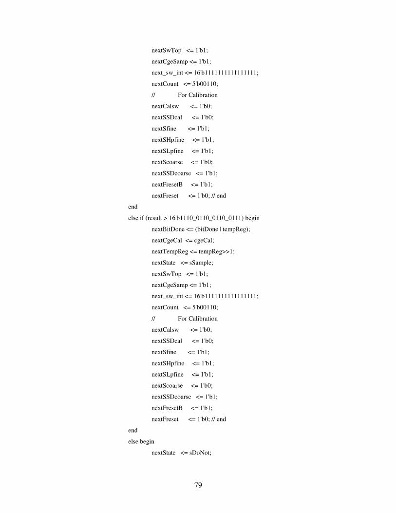
79
nextSwTop <= 1'b1;
nextCgeSamp <= 1'b1;
next_sw_int <= 16'b1111111111111111;
nextCount <= 5'b00110;
// For Calibration
nextCalsw <= 1'b0;
nextSSDcal <= 1'b0;
nextSfine <= 1'b1;
nextSHpfine <= 1'b1;
nextSLpfine <= 1'b1;
nextScoarse <= 1'b0;
nextSSDcoarse <= 1'b1;
nextFresetB <= 1'b1;
nextFreset <= 1'b0; // end
end
else if (result > 16'b1110_0110_0110_0111) begin
nextBitDone <= (bitDone | tempReg);
nextCgeCal <= cgeCal;
nextTempReg <= tempReg>>1;
nextState <= sSample;
nextSwTop <= 1'b1;
nextCgeSamp <= 1'b1;
next_sw_int <= 16'b1111111111111111;
nextCount <= 5'b00110;
// For Calibration
nextCalsw <= 1'b0;
nextSSDcal <= 1'b0;
nextSfine <= 1'b1;
nextSHpfine <= 1'b1;
nextSLpfine <= 1'b1;
nextScoarse <= 1'b0;
nextSSDcoarse <= 1'b1;
nextFresetB <= 1'b1;
nextFreset <= 1'b0; // end
end
else begin
nextState <= sDoNot;
80
nextCgeCtrlF <= (bitDone | tempReg);
end
end
end
end
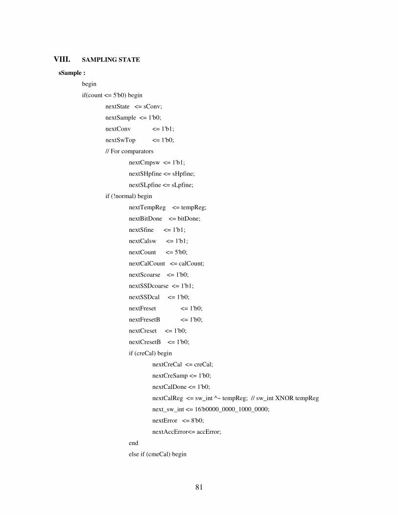
81
VIII. SAMPLING STATE
sSample :
begin
if(count <= 5'b0) begin
nextState <= sConv;
nextSample <= 1'b0;
nextConv <= 1'b1;
nextSwTop <= 1'b0;
// For comparators
nextCmpsw <= 1'b1;
nextSHpfine <= sHpfine;
nextSLpfine <= sLpfine;
if (!normal) begin
nextTempReg <= tempReg;
nextBitDone <= bitDone;
nextSfine <= 1'b1;
nextCalsw <= 1'b1;
nextCount <= 5'b0;
nextCalCount <= calCount;
nextScoarse <= 1'b0;
nextSSDcoarse <= 1'b1;
nextSSDcal <= 1'b0;
nextFreset <= 1'b0;
nextFresetB <= 1'b0;
nextCreset <= 1'b0;
nextCresetB <= 1'b0;
if (creCal) begin
nextCreCal <= creCal;
nextCreSamp <= 1'b0;
nextCalDone <= 1'b0;
nextCalReg <= sw_int ^~ tempReg; // sw_int XNOR tempReg
next_sw_int <= 16'b0000_0000_1000_0000;
nextError <= 8'b0;
nextAccError<= accError;
end
else if (cmeCal) begin
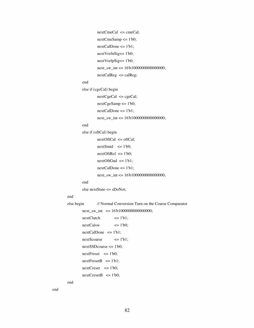
82
nextCmeCal <= cmeCal;
nextCmeSamp <= 1'b0;
nextCalDone <= 1'b1;
nextVrefnSig<= 1'b0;
nextVrefpSig<= 1'b0;
next_sw_int <= 16'b1000000000000000;
nextCalReg <= calReg;
end
else if (cgeCal) begin
nextCgeCal <= cgeCal;
nextCgeSamp <= 1'b0;
nextCalDone <= 1'b1;
next_sw_int <= 16'b1000000000000000;
end
else if (oftCal) begin
nextOftCal <= oftCal;
nextSmid <= 1'b0;
nextOftRef <= 1'b0;
nextOftGnd <= 1'b1;
nextCalDone <= 1'b1;
next_sw_int <= 16'b1000000000000000;
end
else nextState <= sDoNot;
end
else begin // Normal Conversion Turn on the Coarse Comparator
next_sw_int <= 16'b1000000000000000;
nextClatch <= 1'b1;
nextCalsw <= 1'b0;
nextCalDone <= 1'b1;
nextScoarse <= 1'b1;
nextSSDcoarse <= 1'b0;
nextFreset <= 1'b0;
nextFresetB <= 1'b1;
nextCreset <= 1'b0;
nextCresetB <= 1'b0;
end
end
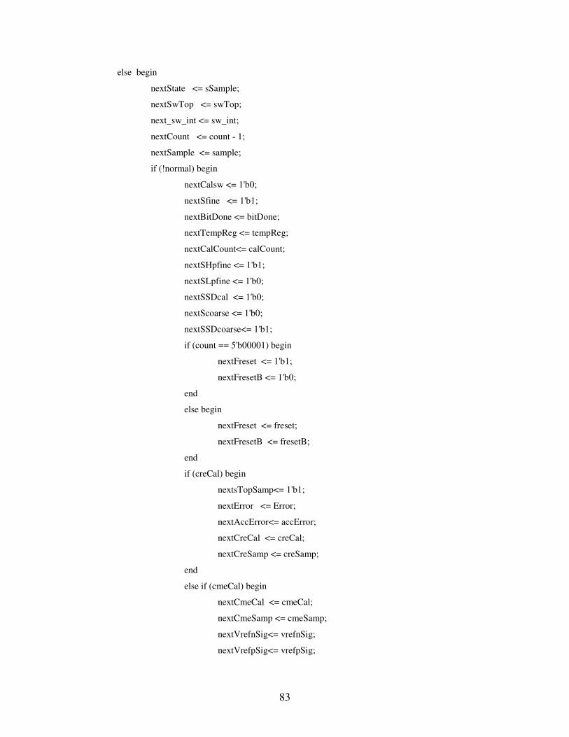
83
else begin
nextState <= sSample;
nextSwTop <= swTop;
next_sw_int <= sw_int;
nextCount <= count - 1;
nextSample <= sample;
if (!normal) begin
nextCalsw <= 1'b0;
nextSfine <= 1'b1;
nextBitDone <= bitDone;
nextTempReg <= tempReg;
nextCalCount<= calCount;
nextSHpfine <= 1'b1;
nextSLpfine <= 1'b0;
nextSSDcal <= 1'b0;
nextScoarse <= 1'b0;
nextSSDcoarse<= 1'b1;
if (count == 5'b00001) begin
nextFreset <= 1'b1;
nextFresetB <= 1'b0;
end
else begin
nextFreset <= freset;
nextFresetB <= fresetB;
end
if (creCal) begin
nextsTopSamp<= 1'b1;
nextError <= Error;
nextAccError<= accError;
nextCreCal <= creCal;
nextCreSamp <= creSamp;
end
else if (cmeCal) begin
nextCmeCal <= cmeCal;
nextCmeSamp <= cmeSamp;
nextVrefnSig<= vrefnSig;
nextVrefpSig<= vrefpSig;
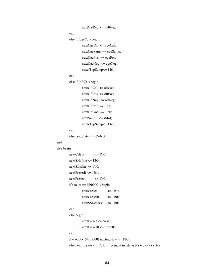
84
nextCalReg <= calReg;
end
else if (cgeCal) begin
nextCgeCal <= cgeCal;
nextCgeSamp <= cgeSamp;
nextCgePos <= cgePos;
nextCgeNeg <= cgeNeg;
nextsTopSamp<= 1'b1;
end
else if (oftCal) begin
nextOftCal <= oftCal;
nextOftPos <= oftPos;
nextOftNeg <= oftNeg;
nextOftRef <= 1'b1;
nextOftGnd <= 1'b0;
nextSmid <= sMid;
nextsTopSamp<= 1'b1;
end
else nextState <= sDoNot;
end
else begin
nextCalsw <= 1'b0;
nextSHpfine <= 1'b0;
nextSLpfine <= 1'b0;
nextFresetB <= 1'b1;
nextFreset <= 1'b0;
if (count == 5'b00001) begin
nextCreset <= 1'b1;
nextCresetB <= 1'b0;
nextSSDcoarse <= 1'b0;
end
else begin
nextCreset <= creset;
nextCresetB <= cresetB;
end
if (count < 5'b10000) nextin_slew <= 1'b0;
else nextin_slew <= 1'b1; // input in_slews for 6 clock cycles

85
end
end
end
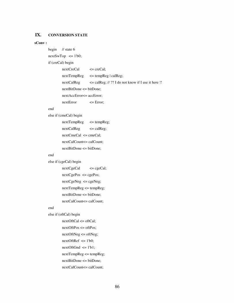
86
IX. CONVERSION STATE
sConv :
begin // state 6
nextSwTop <= 1'b0;
if (creCal) begin
nextCreCal <= creCal;
nextTempReg <= tempReg | calReg;
nextCalReg <= calReg; // ?? I do not know if I use it here !!
nextBitDone <= bitDone;
nextAccError<= accError;
nextError <= Error;
end
else if (cmeCal) begin
nextTempReg <= tempReg;
nextCalReg <= calReg;
nextCmeCal <= cmeCal;
nextCalCount<= calCount;
nextBitDone <= bitDone;
end
else if (cgeCal) begin
nextCgeCal <= cgeCal;
nextCgePos <= cgePos;
nextCgeNeg <= cgeNeg;
nextTempReg <= tempReg;
nextBitDone <= bitDone;
nextCalCount<= calCount;
end
else if (oftCal) begin
nextOftCal <= oftCal;
nextOftPos <= oftPos;
nextOftNeg <= oftNeg;
nextOftRef <= 1'b0;
nextOftGnd <= 1'b1;
nextTempReg <= tempReg;
nextBitDone <= bitDone;
nextCalCount<= calCount;
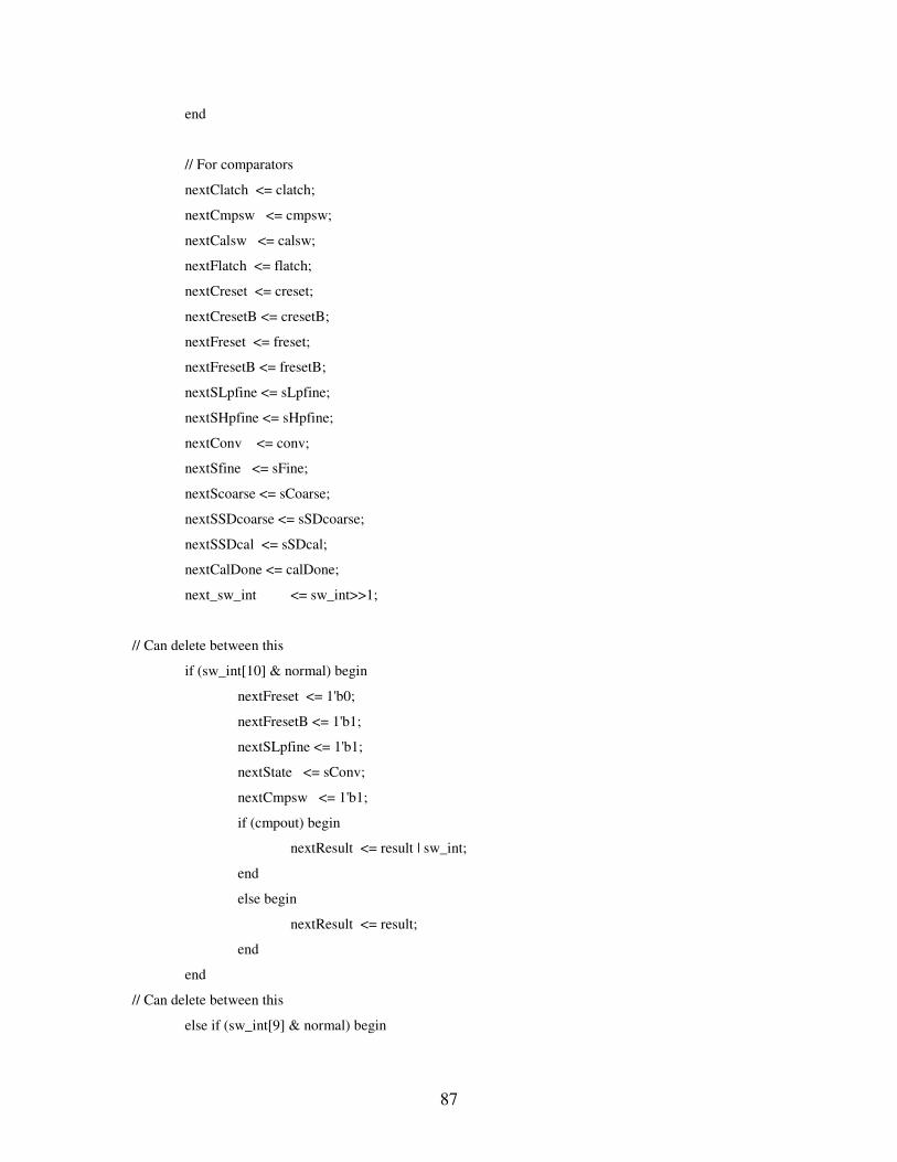
87
end
// For comparators
nextClatch <= clatch;
nextCmpsw <= cmpsw;
nextCalsw <= calsw;
nextFlatch <= flatch;
nextCreset <= creset;
nextCresetB <= cresetB;
nextFreset <= freset;
nextFresetB <= fresetB;
nextSLpfine <= sLpfine;
nextSHpfine <= sHpfine;
nextConv <= conv;
nextSfine <= sFine;
nextScoarse <= sCoarse;
nextSSDcoarse <= sSDcoarse;
nextSSDcal <= sSDcal;
nextCalDone <= calDone;
next_sw_int <= sw_int>>1;
// Can delete between this
if (sw_int[10] & normal) begin
nextFreset <= 1'b0;
nextFresetB <= 1'b1;
nextSLpfine <= 1'b1;
nextState <= sConv;
nextCmpsw <= 1'b1;
if (cmpout) begin
nextResult <= result | sw_int;
end
else begin
nextResult <= result;
end
end
// Can delete between this
else if (sw_int[9] & normal) begin
88
nextFreset <= 1'b1;
nextFresetB <= 1'b0;
nextSLpfine <= 1'b1;
nextState <= sConv;
nextCmpsw <= 1'b1;
if (cmpout) begin
nextResult <= result | sw_int;
end
else begin
nextResult <= result;
end
end
// Resolve hysteresis during Normal Conversion
if (sw_int[8] & normal) begin
nextState <= sConv2;
nextAccError<= accError;
next_sw_int <= 16'b0;
nextDecD <= 1'b0;
nextConv <= 1'b1;
// For comparators
nextClatch <= 1'b0;
nextCmpsw <= 1'b1;
nextFlatch <= 1'b1;
nextCalDone <= 1'b1;
nextSfine <= 1'b1;
nextScoarse <= 1'b0;
nextSLpfine <= 1'b1;
nextSSDcoarse <= 1'b1;
nextCreset <= 1'b0;
nextCresetB <= 1'b1;
nextFresetB <= 1'b0;
nextFreset <= 1'b0;
if (cmpout) begin
nextResult <= result | sw_int;
89
nextD <= result | sw_int;
end
else begin
nextResult <= result;
nextD <= result;
end
end
// Reset state between lp->hp fine comp-mode transition
/*else if (sw_int[4] & normal) begin
nextState <= sReset; // Reset State
nextFreset <= 1'b1;
nextCmpsw <= 1'b0;
nextSfine <= 1'b1;
nextSHpfine <= 1'b1;
nextSLpfine <= 1'b0;
next_sw_int <= sw_int;
nextFlatch <= 1'b0;
nextAccError <= accError;
//nextTempReg <= control;
if (cmpout) begin
nextResult <= result | sw_int;
end
else nextResult <= result;
end
// Error elimination for lp->hp fine comp-mode transition
else if (sw_int[3] & normal) begin // Error correctio during Lp-> Hp transition
nextState <= sConv4;
nextSHpfine <= 1'b1;
nextSLpfine <= 1'b0;
nextFlatch <= 1'b1;
next_sw_int <= sw_int;
nextTempReg <= result|sw_int;
if (cmpout) begin
// Get the comparison result for D+1
nextD <= {(result[15:3]|sw_int[15:3]) + 1'b1, 3'b0};
nextDecD <= 1'b1;
nextTempReg <= result;
90
end
else begin
// Get the comparison result for D-1
nextD <= {(result[15:3]|sw_int[15:3]) - 1'b1, 3'b0};
nextDecD <= 1'b0;
nextTempReg <= result;
end
end*/
// CRE calibration
else if (sw_int[0] & creCal) begin
nextState <= sCreCalc1;
nextCreCal <= creCal;
nextsTopSamp<= 1'b1;
// For Calibration
nextCalsw <= 1'b1;
nextSSDcal <= 1'b0;
nextSfine <= 1'b1;
nextSHpfine <= 1'b1;
nextSLpfine <= 1'b1;
nextScoarse <= 1'b0;
nextSSDcoarse <= 1'b1;
nextFresetB <= 1'b1;
nextFreset <= 1'b0; // end
if (cmpout) begin
nextResult <= (result | sw_int);
end
else nextResult <= result;
end
// CME calibration
// CME calibration sample Vrefp
else if(sw_int[0] & cmeCal) begin
if (calCount == 3'b010 | calCount == 3'b100) begin
//nextVrefpSig <= 1'b0;
nextState <= sCmeCalc; // calculate Ecm (error)
nextCmeCal <= cmeCal;
nextCalCount <= calCount;
91
end
else begin
nextState <= sSample;
nextCmeSamp <= 1'b1; // High only during Ref Voltage Sampling
nextCmeCal <= cmeCal; // to be remained high entire CME cal
//nextsCme <= 1'b1;
next_sw_int <= 16'b1111111111111111;
nextVrefpSig<= 1'b1; // Sample Vrefp
nextSwTop <= 1'b0;
nextCmpsw <= 1'b0;
nextCalCount<= calCount + 1'b1;
nextCount <= 5'b00110;
// For Calibration
nextCalsw <= 1'b1;
nextSSDcal <= 1'b0;
nextSfine <= 1'b1;
nextSHpfine <= 1'b1;
nextSLpfine <= 1'b1;
nextScoarse <= 1'b0;
nextSSDcoarse <= 1'b1;
nextFresetB <= 1'b1;
nextFreset <= 1'b0; // end
end
if (cmpout) nextCalReg <= (result | sw_int) - calReg;
else nextCalReg <= result - calReg;
end
// Offset Calibration
else if (sw_int[0] & oftCal) begin // offset calibration
nextState <= sOftCalc;
nextOftCal <= oftCal;
if (cmpout) begin
nextResult <= result | sw_int;
end
else nextResult <= result;
end
// Gain Error Calibration
else if (sw_int[0] & cgeCal) begin
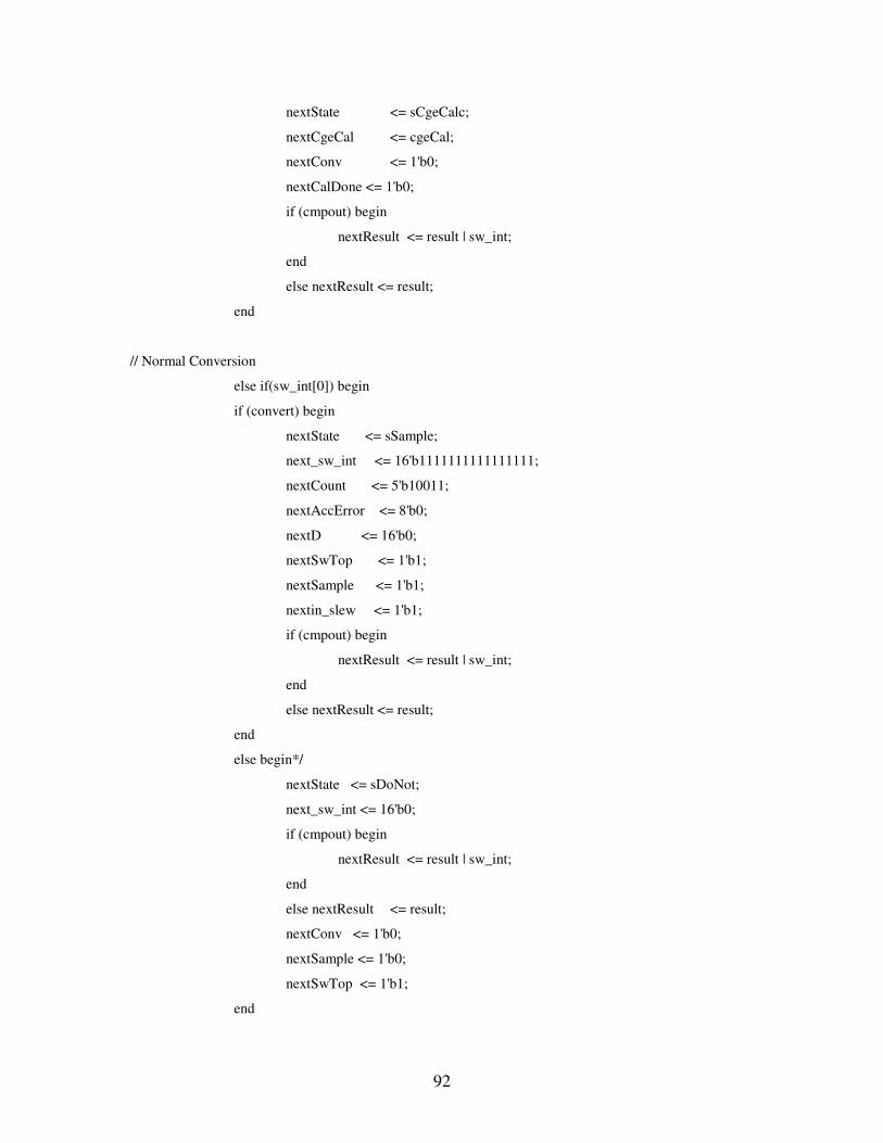
92
nextState <= sCgeCalc;
nextCgeCal <= cgeCal;
nextConv <= 1'b0;
nextCalDone <= 1'b0;
if (cmpout) begin
nextResult <= result | sw_int;
end
else nextResult <= result;
end
// Normal Conversion
else if(sw_int[0]) begin
if (convert) begin
nextState <= sSample;
next_sw_int <= 16'b1111111111111111;
nextCount <= 5'b10011;
nextAccError <= 8'b0;
nextD <= 16'b0;
nextSwTop <= 1'b1;
nextSample <= 1'b1;
nextin_slew <= 1'b1;
if (cmpout) begin
nextResult <= result | sw_int;
end
else nextResult <= result;
end
else begin*/
nextState <= sDoNot;
next_sw_int <= 16'b0;
if (cmpout) begin
nextResult <= result | sw_int;
end
else nextResult <= result;
nextConv <= 1'b0;
nextSample <= 1'b0;
nextSwTop <= 1'b1;
end
93
// Bit cycle and get result
else begin
/*if (normal) begin
nextTempReg <= control;
end
else nextTempReg <= tempReg;*/
if (cmpout) begin
nextResult <= result | sw_int;
if (creCal) nextAccError <= accError; // only during CRE calibration
else nextAccError<= (accError + bitErr); // during normal conversion + other
cali
end
else begin
nextResult <= result;
nextAccError<= accError;
end
//nextFreset <= freset;
//nextFresetB<= fresetB;
nextCreset <= creset;
nextCresetB <= cresetB;
/*if ((sw_int[10] | sw_int[9]) & !creCal & !cmeCal & !cgeCal) // May 20 - 11,10,9 -->
Look at if--else (above)
nextFreset <= freset<<1;
else nextFreset <= freset;*/
end
end
94
X. HYSTERESIS REMOVAL
sConv2:
begin // state 7
nextCalDone <= 1'b1;
nextSwTop <= 1'b0;
nextCmeCal <= cmeCal;
nextCalReg <= calReg; // store temp-Result during CME cal
nextCalCount<= calCount;
nextTempReg <= tempReg;
nextBitDone <= bitDone;
nextSfine <= 1'b1;
nextSLpfine <= 1'b1;
// For comparators
nextCmpsw <= 1'b1;
nextFreset <= 1'b0;
nextFresetB <= 1'b0;
nextFlatch <= flatch;
nextCreset <= 1'b0;
nextCresetB <= 1'b1;
//
if (result == 16'b1111111100000000) begin
nextD <= result;
end
else begin
nextD <= {D[15:8] + 1'b1, 8'b0};
end
nextResult <= result;
nextSfine <= 1'b1;
next_sw_int <= {result[15:8] - 1'b1, 8'b0}; //****
if (cmpout)
nextDecD <= 1'b1;
else nextDecD <= 1'b0;
nextState <= sConv3;
nextConv <= 1'b1;
nextAccError <= accError;
end
95
// *************************************************************** //
sConv3:
begin // state 8
nextCalDone <= 1'b1;
nextSwTop <= 1'b0;
nextCmeCal <= cmeCal;
nextCalReg <= calReg; // store temp-Result during CME cal
nextCalCount<= calCount; // for CME cal
nextTempReg <= tempReg;
nextBitDone <= bitDone;
// For comparators
nextCmpsw <= 1'b1;
nextFreset <= 1'b0;
nextFresetB <= 1'b0;
nextFlatch <= flatch;
nextCreset <= 1'b0;
nextCresetB <= 1'b1;
//
nextD <= 16'b0;
nextSfine <= 1'b1;
nextSLpfine <= 1'b1;
next_sw_int <= 16'b0000000010000000;
nextState <= sConv;
nextConv <= 1'b1;
if (!cmpout & !dec_D) begin
if (result == 16'b0) begin
nextResult <= result;
nextAccError <= accError;
end
else begin
nextResult <= {result[15:8] - 1'b1, 8'b0};
nextAccError<= totErr; //******************
end
end
else if (cmpout & dec_D) begin
if (result == 16'b1111111100000000) begin
96
nextResult <= result;
nextAccError <= accError;
end
else begin
nextResult <= {result[15:8] + 1'b1, 8'b0};
nextAccError<= accErrN; //******************
end
end
else begin
nextResult <= result;
nextAccError<= accError; //******************
end
end