Embed Size (px)
Citation preview
A simpler and faster method for SVM implementation
Santiago de Pablo, Alexis B. Rey*, Luis C. Herrero and José M. Ruiz UNIVERSITY OF VALLADOLID
(*) TECHNICAL UNIVERSITY OF CARTAGENA E.T.S. Ingenieros Industriales, Paseo del Cauce, s/n.
47011, Valladolid, Spain Tel.: +34 983 42 33 44 Fax: +34 983 42 33 10
E-Mail: [email protected] URL: http://www.dte.eis.uva.es/epYme
Acknowledgements Authors would like to acknowledge the partial financial support of the Junta de Castilla y León under grants VA004B06 and VA021B06.
Keywords Vector control, Pulse Width Modulation, Modulation strategy, Converter control, VSI.
Abstract Space Vector Modulation is perhaps the common technique mostly applied to drive three-phase voltage-source inverters. During every switching period it calculates three duty cycles in order to generate a suitable pulse sequence. This paper presents a new, faster and, most important, simpler method to compute these time values without using either trigonometric functions or even Clarke or Park transformations. The result is a light-weight algorithm easier to implement in small digital signal processors or microcontrollers. The relationship between SVM and PWM is also explained.
Introduction Space Vector Modulation (SVM) was originally developed by Van der Broeck et al. [1] as a vector approach to pulse width modulation (PWM) for three-phase voltage source inverters (VSI). Compared with the former three-phase sinusoidal modulation method (SPWM) it has the advantages of lower current harmonics and a possible higher modulation index [1]. This technique has a wide linear modulation range with no need of distorted modulation and it also guarantees that only one switch changes at any time. During two decades, SVM has been considered a reference for most analysis, comparisons and physical verifications [2]–[6]. Recently, some research efforts have been directed to develop multilevel inverters and matrix converters based on SVM method [7], [8]. However, recent studies have been more critical with SVM and several solutions in time domain are defended as simpler and/or faster [9], [10]. This paper improves the equations used to compute SVM duty cycles for two-level inverters and reveals its relationship with carrier-based PWM methods.
Classical SVM The structure of a typical three-phase voltage source power inverter is shown in Fig. 1. The relationship between switching variables (Su, Sv, Sw) and line-to-line voltages (VUV, VVW, VWU) is given by (1), where Vdc is the bus voltage and Sk is '1' or '0' when the upper or lower transistor of phase k is on, respectively. Choosing a neutral point 'N' that satisfies (2) and equating (1) it yields (3).
A simpler and faster method for SVM implementation PABLO Santiago De
EPE 2007 - Aalborg ISBN : 9789075815108 P.1

Fig. 1: Hex bridge, with the upper switches used to define switching states.
−−
−=
w
v
u
dc
WU
VW
UV
SSS
VVVV
·101110
011 (1)
0=++ WNVNUN VVV (2)
−−−−−−
=
w
v
u
dc
WN
VN
UN
SSS
VVVV
·211121112
31 (3)
Applying the Clarke transformation to these output voltages, equation (4), it leads to a 2-D space vector V with the same instantaneous information in a stationary reference frame. The behavior of this vector is well known: when a balanced and sinusoidal three phase voltage system is analyzed, with constant magnitude Vo and constant frequency ωo, the space voltage representation is a vector of constant length Vo rotating with constant angular speed ωo. Likewise, when this transformation is applied to the inverter phase-to-neutral voltages the result are eight different vectors according to the eight possible switches states (see equation (5) and Fig. 2). The rotating reference vector vo* must be inside the hexagon for linear modulation.
=
= −
−−
WN
VN
UN
VVV
VV
·0 3
333
31
31
32
β
αV (4)
Fig. 2: Space vectors of inverter voltages and other definitions.
A simpler and faster method for SVM implementation PABLO Santiago De
EPE 2007 - Aalborg ISBN : 9789075815108 P.2

7,0,0
6,...,2,1,)3/)(1(32
==== −
xxeV
x
xjdcx
VV π
(5)
To obtain the required output space vector vo*, that usually is a rotating vector with constant module and pulsation, conduction times of the inverter switches are modulated according to the angle and magnitude of that reference. The null vectors (VZ ≡ V0 = V7), and two space vectors adjacent to vo*, Vi and Vj, are chosen and modulated as follows: jjiiZZo ddd VVVv ++=∗ (6) Duty cycles of these vectors can be computed using polar coordinates (see [1] for further details) by means of (7) [1], [6], [10], [11], where θr is the relative angle between vo* and Vi vectors (0 ≤ θr ≤ π/3), and m is the modulation index (0 ≤ m ≤ 1) defined as m = √3·Vo/Vdc.
jiZ
rj
ri
ddd
mdmd
−−=
=−=
1
)·sin()·sin( 3
θθπ
(7)
This method calculates all information needed to generate suitable switching sequences (usually d0 = d7 = dZ / 2), but its straightforward implementation needs the computation of two 'sin(x)' functions [11] and one division by Vdc. This division can be computed using a polynomial approach, but trigonometric functions require either big lookup tables or a time consuming process. In addition, a previous operation is required: the sector of vo* must be determined, because it is necessary to know which one of the inverter voltage vectors are adjacent to the given reference (see Fig. 2), in order to solve (7). For this operation the reference phase value can be used [12].
A known improvement of SVM The objective of space vector PWM technique is to approximate the reference phase-to-neutral voltage vector [vUN* vVN* vWN*]T or its equivalent space vector vo* by a combination of the eight switching patterns. One simple means of approximation is to require the average output of the inverter in a small switching period TS to be the same as the average of vo* in the same period, which for a switching frequency much higher than the fundamental one it is assumed constant during one switching cycle. This requirement, known as “per-carrier-cycle volt-second balance” principle [5], has been shown in (6), but can be exploited in a different way:
So
Tt
tojjiiZZ TdtTTT
S
·∗+
∗ ≅=++ ∫ vv·V·V·V (8)
As the value of TZ has no effect in (8) because of the null magnitude of VZ, this equation can be used to compute Ti and Tj as shown in (9), where P is defined at (10); TZ is finally computed using (11).
So
o
j
i Tvv
TT
·· *
*1
=
−
β
αP (9)
≡
ββ
αα
ji
ji
VVVV
P (10)
jiSZ TTTT −−= (11)
A simpler and faster method for SVM implementation PABLO Santiago De
EPE 2007 - Aalborg ISBN : 9789075815108 P.3

The matrix P is sector dependent and can be arranged (see table I) in such a way that a one-upper-switch-on vector (V1, V3 or V5) is chosen as Vi and a two-upper-switches-on vector (V2, V4 or V6) is Vj. Hence it is easier for a digital signal processor (DSP) the generation of the typical V0 - Vi - Vj - V7 - Vj - Vi - V0 sequence during TS, thus reducing the average switching frequency. These expressions have been widely used [8], [9], [12] rather than (7) because it is easy to implement them on DSP processors.
Table I: Transformation matrices for each sector under SVM.
Sector I Sector II Sector III
dcV·0 3
331
32
= P
Vi = V1 and Vj = V2
dcV·33
33
31
31
=
−
P
Vi = V3 and Vj = V2
dcV·03
332
31
=
−−
P
Vi = V3 and Vj = V4
Sector IV Sector V Sector VI
dcV·03
332
31
= −
−−
P
Vi = V5 and Vj = V4
dcV·3
33
331
31
= −−
−
P
Vi = V5 and Vj = V6
dcV·0 3
331
32
= − P
Vi = V1 and Vj = V6
Proposed method for SVM Computations involved in (9) and (11) are not complex and several implementations of that method are used in the reviewed literature. However, a simpler set of equations can be obtained solving them in an analytical way. To do so, it will be assumed, without loss of generality, a reference phase voltage between 0 and π/3, thus V1 and V2 will be used jointly with V0 and V7 to generate vo*. Equation (9) and table I yield to:
So
o
dc
dcdc Tvv
VVV
TT
··0 *
*1
33
31
32
2
1
=
−
β
α (12)
Equating (12) it leads to:
Sdc
o
Sdc
oo
TV
vT
TV
vvT
··3
···
*
2
*23*
23
1
β
βα
=
−=
(13)
However, applying (4) to (13) it yields to even simpler expressions (see [6] for a different approach):
Sdc
WNVN
Sdc
VNUN
TV
vvT
TV
vvT
·
·
**
2
**
1
−=
−= (14)
In the same way, equating (11) it yields to the following expression, related with (14):
Sdc
UNWNZ T
VvvT ·1
**
−+= (15)
A simpler and faster method for SVM implementation PABLO Santiago De
EPE 2007 - Aalborg ISBN : 9789075815108 P.4
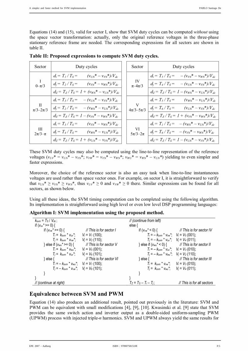
Equations (14) and (15), valid for sector I, show that SVM duty cycles can be computed without using the space vector transformation: actually, only the original reference voltages in the three-phase stationary reference frame are needed. The corresponding expressions for all sectors are shown in table II.
Table II: Proposed expressions to compute SVM duty cycles.
Sector Duty cycles
Sector Duty cycles
di = T1 / TS = (vUN* – vVN*)/Vdc
di = T5 / TS = – (vVN* – vWN*)/Vdc
dj = T2 / TS = (vVN* – vWN*)/Vdc
dj = T4 / TS = – (vUN* – vVN*)/Vdc I
0–π/3 dZ = TZ / TS = 1 + (vWN* – vUN*)/Vdc
IV π–4π/3
dZ = TZ / TS = 1 – (vWN* – vUN*)/Vdc
di = T3 / TS = – (vUN* – vVN*)/Vdc
di = T5 / TS = (vWN* – vUN*)/Vdc
dj = T2 / TS = – (vWN* – vUN*)/Vdc
dj = T6 / TS = (vUN* – vVN*)/Vdc II
π/3–2π/3 dZ = TZ / TS = 1 – (vVN* – vWN*)/Vdc
V 4π/3–5π/3
dZ = TZ / TS = 1 + (vVN* – vWN*)/Vdc
di = T3 / TS = (vVN* – vWN*)/Vdc
di = T1 / TS = – (vWN* – vUN*)/Vdc
dj = T4 / TS = (vWN* – vUN*)/Vdc
dj = T6 / TS = – (vVN* – vWN*)/Vdc III
2π/3–π dZ = TZ / TS = 1 + (vUN* – vVN*)/Vdc
VI 5π/3–2π
dZ = TZ / TS = 1 – (vUN* – vVN*)/Vdc These SVM duty cycles may also be computed using the line-to-line representation of the reference voltages (vUV* = vUN* – vVN*; vVW* = vVN* – vWN*; vWU* = vWN* – vUN*) yielding to even simpler and faster expressions. Moreover, the choice of the reference sector is also an easy task when line-to-line instantaneous voltages are used rather than space vector ones. For example, on sector I, it is straightforward to verify that vUN* ≥ vVN* ≥ vWN*, thus vUV* ≥ 0 and vVW* ≥ 0 there. Similar expressions can be found for all sectors, as shown below. Using all these ideas, the SVM timing computation can be completed using the following algorithm. Its implementation is straightforward using high level or even low level DSP programming languages:
Algorithm I: SVM implementation using the proposed method. ksvm = TS / Vdc ; if (vuv* >= 0) if (vvw* >= 0) // This is for sector I Ti = ksvm * vuv*; Vi = V1 (100); Tj = ksvm * vvw*; Vj = V2 (110); else if (vwu* >= 0) // This is for sector V Ti = ksvm * vwu*; Vi = V5 (001); Tj = ksvm * vuv*; Vj = V6 (101); else // This is for sector VI Ti = – ksvm * vwu*; Vi = V1 (100); Tj = – ksvm * vvw*; Vj = V6 (101); // (continue at right)
// (continue from left) else if (vvw* < 0) // This is for sector IV Ti = – ksvm * vvw*; Vi = V5 (001); Tj = – ksvm * vuv*; Vj = V4 (011); else if (vwu* < 0) // This is for sector II Ti = – ksvm * vuv*; Vi = V3 (010); Tj = – ksvm * vwu*; Vj = V2 (110); else // This is for sector III Ti = ksvm * vvw*; Vi = V3 (010); Tj = ksvm * vwu*; Vj = V4 (011); TZ = TS – Ti – Tj ; // This is for all sectors
Equivalence between SVM and PWM Equation (14) also produces an additional result, pointed out previously in the literature: SVM and PWM can be equivalent with small modifications [4], [9], [10]. Kwasinski et al. [9] state that SVM provides the same switch action and inverter output as a double-sided uniform-sampling PWM (UPWM) process with injected triple-n harmonics. SVM and UPWM always yield the same results for
A simpler and faster method for SVM implementation PABLO Santiago De
EPE 2007 - Aalborg ISBN : 9789075815108 P.5

the active vectors, but SVM leaves a degree of freedom in the partitioning of zero vectors [5], [6], likewise PWM methods may add different zero-sequence signals to the modulation waves [5]. This paper agrees with that conclusion, but presents a different approach to this issue. Firstly consider Fig. 3. It represents a classical PWM arrangement with distorted modulation, using ±Vdc/2 as carrier limits: a triangular waveform with 25% magnitude (in bold dashed line) has been added to all arm voltage references to extend up the modulation index [2], [10]; as this signal only has triple-n harmonics and they form zero-sequence systems, they produce no currents in floating loads. All voltages in this figure are referred to the DC bus midpoint, named 'M' in Fig. 1: carrier limits, phase voltage modulators, and also the AC neutral point voltage, vNM, whose significant component matches the zero-sequence signal injected.
Fig. 3: Classical PWM arrangement with distorted modulators. The same situation may be considered from a different point of view for symmetrical loads. When all voltages are referred to the AC neutral floating point main voltage, named 'N', Fig. 3 is transformed into Fig. 4. Phase-to-neutral voltage references have no zero-sequence component (their sum is zero), so they have no distortion; the voltage of the DC bus midpoint, named ‘M’, referred to the load neutral point, is also a triangular wave (at least its significant component) but now its sign is changed; finally, carrier limits are not constant, because of the variation of the vMN voltage main component. Noticeably, a digital implementation of this arrangement would be complicated, but it reveals interesting details.
Fig. 4: A different perspective of PWM, referring all signals to the load neutral point. In this alternative PWM arrangement (Fig. 4), a high frequency carrier signal of constant height (equal to Vdc), but with time varying limits, intercepts three pure-sinusoidal phase-to-neutral voltage references and decides the switch states as usual ('0' when carrier is above each reference, '1' when it is below) [2]. Then, it follows that, for sector I (these results can be applied to all sectors), the time
A simpler and faster method for SVM implementation PABLO Santiago De
EPE 2007 - Aalborg ISBN : 9789075815108 P.6

period required by vector V1 (100) is proportional to TS/Vdc, an almost constant value, and also proportional to the difference between phase voltages vUN* and vVN* (matching what was stated in table II and algorithm I). In the same way, vector V2 (110) must be proportional to the difference between phase voltages vVN* and vWN*. Null vectors V0 (000) and V7 (111) fill the spare time at 50%. Actually, the same results are obtained when Fig. 3 is used instead of Fig. 4, because zero-sequence components modify all modulator waves in the same amount at any time. A second detail clearly shown in Fig. 4 is the relationship between vMN and the partitioning of TZ: active vectors (Vi and Vj) are related only with the line-to-line output voltages [6], while zero vectors (V0 and V7) decide the shape of the zero-sequence voltage injected. A triangular wave results for vMN when T0 equals T7, but other options are clearly possible [5], [6].
Simulations and experimental results Several simulations and physical implementations have been developed to validate these results. A 10 kVA 3-phase VSI connected to an L-R-E load (see the structure in Fig. 1) has been simulated using our own graphical environment [13]; its main results are shown in Figs. 5 and 6. In such simulation, the DC-link was Vdc = 595 V, the line-to-line 50 Hz output voltage was Vac = 400 V (rms), the switching frequency was fS = 6 kHz and the electrical load was resistive (R = 16 Ω) connected by means of a simple inductance (L = 2000 µH). Inverter duty cycles were computed on every switching period using the equations shown in table II with d0 = d7, then PWM signals were generated using a triangular carrier with a resolution of 250 ns neglecting dead-band effects, and all simulated signals were sampled at 200 KSPS. The output voltage (Fig. 5-c) is so noisy because of the pure resistive nature of the load (i.e. E = 0 V).
Fig. 5: Simulation of a three-phase 10 kVA VSI connected to a symmetrical and pure resistive load. Four images are (a) inverter phase-to-neutral voltage for phase 'U', (b) inverter gate signals through a low-pass filter (second order at 1 kHz), (c) phase-to-neutral voltages on the resistive load, and (d) neutral point voltage, referred to the DC midpoint, through a low-pass filter (second order at 1 kHz).
A simpler and faster method for SVM implementation PABLO Santiago De
EPE 2007 - Aalborg ISBN : 9789075815108 P.7

Fig. 6: Frequency spectrum, from DC to 20 kHz, computed for Fig. 5-c. In order to investigate the validity of these ideas and their practical capabilities, experimental results were obtained by applying the proposed SVM method using a Texas Instruments TMS320F2812 development board that achieves 150 MIPS. The source code was written in C and compiled using Code Composer Studio. It generates three 50 Hz sinusoidal references, selects the inverter sector and computes all switching duty cycles based on the proposed algorithm; then it configures three PWM generators to work at 5 kHz. The main results can be seen in Figs. 7 and 8.
Fig. 7: Inverter 5 kHz gate signal generated by a TMS320F2812 DSP using the proposed SVM technique, with no filtering (CH1, above) and filtered with R = 2.2 kΩ and C = 0.27 µF, i.e. first order at 1680 Hz (CH2, below).
Fig. 8: The difference between two gate signals (CH1 and CH2, above) will produce a line-to-line output voltage free of triple-n harmonics (Matem = CH1 – CH2, in the middle).
Conclusion This paper has presented a new, faster and, most important, simpler method to compute SVM duty cycles without using either trigonometric functions or even Park or Clarke transformations. The result is a light-weight algorithm easier to understand. Its implementation is straightforward in low-end digital signal processors or even small microcontrollers. The relationship between SVM and PWM has also been explained using a different point of view: referring all voltages to the AC neutral point. Doing so, arm voltage references have no distortion, but time varying limits appear for PWM carrier. The advantage is that they allow an equally wide linear modulation range with no need of distorted modulation, and it also explains how triple-n harmonics are injected with no effects on inverter output voltages when floating and symmetrical loads are used.
References [1] H.W. Van der Broeck, H.C. Skudelny and G.V. Stanke: “Analysis and realization of a pulsewidth modulator
based on voltage space vectors”, IEEE Trans. on Industry Applications, vol. 24, no. 1, pp. 142-150, January/February 1988.
A simpler and faster method for SVM implementation PABLO Santiago De
EPE 2007 - Aalborg ISBN : 9789075815108 P.8

[2] P.G. Handley and J.T. Boys: “Space Vector Modulation: an engineering review”, 4th Int. Conf. on Power Electronics and Variable-Speed Drives, pp. 87-91, July 1990.
[3] J. Holtz: “Pulsewidth modulation for electronic power conversion”, Proceedings of the IEEE, vol. 82, no. 8, pp. 1194-1214, August 1994.
[4] D.G. Holmes: “The Significance of Zero Space Vector Placement for Carrier-Based PWM Schemes”, IEEE Trans. on Industry Applications, vol. 32, no. 5, pp. 1122-1129, September/October 1996.
[5] A.M. Hava, R.J. Kerkman and T.A. Lipo: “A high-performance generalized discontinuous PWM algorithm”, IEEE Trans. on Industry Applications, vol. 34, no. 5, pp. 1059-1071, September/October 1998.
[6] K. Zhou and D. Wang: “Relationship between space-vector modulation and three-phase carrier-based PWM: a comprehensive analysis”, IEEE Trans. on Industrial Electronics, vol. 49, no. 1, pp. 186-196, February 2002.
[7] C. Klumpner and F. Blaabjerg: “Modulation Method for a Multiple Drive System based on a Two-Stage Direct Power Conversion Topology with Reduced Input Current Ripple”, IEEE Trans. on Power Electronics, vol. 20, no. 4, pp. 922-929, July 2005.
[8] A.K. Gupta and A.M. Khambadkone: “A Space Vector PWM Scheme for Multilevel Inverters Based on Two-Level Space Vector PWM”, IEEE Trans. on Industrial Electronics, vol. 53, no. 5, pp. 1631-1639, October 2006.
[9] A. Kwasinski, P.T. Krein, and P.L. Chapman: “Time domain comparison of pulse-width modulation schemes”, IEEE Power Electronics Letters, vol. 1, no. 3, pp. 64-68, September 2003.
[10] S. Bowes and Y.S. Lai: “The relationship between space-vector modulation and regular-sampled PWM”, IEEE Trans. on Industrial Electronics, vol. 44, no. 5, pp. 670-679, October 1997.
[11] J. Youm and B. Kwon: “An Effective Software Implementation of the Space-Vector Modulation”, IEEE Trans. on Industrial Electronics, vol. 46, no. 4, pp. 866-868, August 1999.
[12] Z. Yu and D. Figoli: “AC induction motor control using constant V/Hz principle and space vector PWM technique with TMS320C240”, Texas Instruments Application Report SPRA284A, April 1998.
[13] epYme workgroup: “SimulEP, a web simulator for Power Electronics”, on-line at <http://www.dte.eis. uva.es/epYme/SimulEP.php>, updated on May 2007.
A simpler and faster method for SVM implementation PABLO Santiago De
EPE 2007 - Aalborg ISBN : 9789075815108 P.9