Embed Size (px)
Citation preview

N A S A
0 cv m
e U
I
4 c/)
4 z
~ ~- - . .
*
C O N T R A C T O R
R E P O R T C R - 5 2 (
1
A SPACECRAFT DIGITAL STABILIZATION AND CONTROL SYSTEM STUDY
Prepared by LEAR SIEGLER, INC. Grand Rapids, Mich.
for
https://ntrs.nasa.gov/search.jsp?R=19660022565 2018-09-06T03:03:39+00:00Z

TECH LIBRARY KAFB, NY
A SPACECRAFT DIGITAL STABILIZATION
AND CONTROL SYSTEM STUDY
By H. C. Daubert, E. W. Hoffman, and T. E. Perfitt
Distribution of this report is provided in the interest of information exchange. Responsibility for the contents resides in the author or organization that prepared it.
@Lear Siegler, Inc.
Prepared under Contract No. NASw- 1004 by
Grand Rapids, Mich. LEAR SIEGLER, INC.
for
': NATIONAL AERONAUTICS AND SPACE ADMINISTRATION "_ ~
' Far sale by the Clearinghouse for Federal Scientific and Technical Information Springfield, Virginia 22151 - Price $4.00

ABSTRACT
A study and experimental evaluation was performed to apply digital techniques to the problem of increasing the reliability and accuracy of spacecraft stabilization and control systems, as the sophistication and duration of spacecraft missions are increased. To meet these more stringent requirements, the use of digital systems utilizing monolithic integrated microelectronics is indicated.
Of major consideration during this study were the exami- nation of mathematical techniques for systems analysis and the investigation of problems involved in fabricating systems using integrated circuits. A specific type of loop was postulated, designed and constructed with monolithic integrated circuits. A state-space model of this system was written and programmed for computer evaluation. The mathematical model of this system is described and a comparison .made between the predicted performance and actual system performance tests made on an air-bearing simulator. The design logic, fabrication problems, and a computer-aided design optimization method are described.
ii
T A B L E O F C O N T E N T S
Section
LIST OF ILLUSTRATIONS
1 INTRODUCTION
1.1 Requirements of Spacecraft Control
1.2 Selection of Means for Meeting
1.2. 1 Analog Systems 1.2.2 Digital Systems 1.2.3 Component Selection 1.2.4 Optimum System and Component
Systems
Requirements
Approach
Approach 1.2.5 Summary of Advantages of Selected
1.3 The Experimental System
2 DESIGN METHODOLOGY
2.1 2.2 2.3 2.4 2.4.1 2.4.2 2.4.3 2.4.4 2.4.5 2.4. 6 2.4.7 2.4.8 2.4.9 2.4.10 2.4.11
Objective The State Model LSI Spacecraft Simulation Model System Logic Design
Word Length and Rate Control Unit Adder/Subtracter Command Register Proportional Register Integrator Register Output Register Buffer Register Rate Multiplier Digital Speed Control Integrator Lockout
Page No.
1-1
1-2
1-2
1-3 1-3 1-6 1-8
1-9
1-11
2-1
2-1 2-1 2-9 2-17 2-17 2-17 2-23 2-27 2-27 2-29 2-29 2-31 2- 31 2-34 2-34
iii

T A B L E O F C O N T E N T S (cont)
Page No. Section
ELECTRONICS UNIT DEVELOPMENT 3- 1 3
3-1 3-1 3-2
3 . 1 3 . 2 3 . 3
Component Selection Package Design Fabrication and Assembly
4 DEBUGGING AND TESTING 4- 1
4. 1 4 . 2
Test Equipment Test Results
4- 2 4- 2
SUMMARY AND RECOMMENDATIONS 5-1 5
RELIABILITY TEST PLAN FOR SPACECRAFT CONTROL SYSTEMS
A- 1 APPENDIX A
GENERAL DESIGN PROCEDURE FOR SPACECRAFT CONTROL SYSTEMS
B- 1 APPENDIX B
c-1 APPENDIX C COMPUTER PROGRAM DATA
R- 1 REFERENCES
iv

Figure No.
6
7
8 9 10
11 12 13 14 15 16 17 18 19
20
21
22
A-1
A-2 . A-3
A-4
L I S T O F I L L U S T R A T I O N S
Title
Comparison of Accuracy and Complexity System Block Diagram Basic System Model Linear, Time Stationary System S-Domain Block Diagram - LSI Simulator
Time-Domain, Non-Linear Model - LSI
Digital Controller Response - Computed
General Data Flow Diagram Master Clock Divider and Timing Index Counter With Truth Tables and
Control Logic Diagram Arithmetic Unit Logic Block Diagram Serial Adder/Subtracter Logic Diagram Output Register Control Logic Binary Rate Multiplier Digital Speed Control Logic Block Diagram Typical Circuit Board and Final Assembly Test Set - Up Strip Chart Recording - Step Response - Phase Plane Recording - Step Response - Strip Chart Recording - Step Response - Phase Plane Recording - Step Response -
System
Simulator System
and Observed
Vietch Diagrams
45 O Command
4 5 O Command
22.5 Command
22.5 Command
Typical Plot of Step Stress Vs. Time to
Typical Plot of Stress Interaction Typical Acceleration Curve Sample Unit Block Diagram - Digital
System Reliability Test
Failure
Page No.
1-4 1-12 2-2 2-3 2-10
2-11
2-16
2-18 2-19 2-21
2-24 2-25 2-26 2-32 2-33 2-35 3-3 4-3 4-4
4-5
4-6
4-7
A-6
A-8 A-10 A-12
V

L I S T O F I L L U S T R A T I O N S (cont)
Figure No. Title
B-1 B-2 B-3
B-4
c-1 c-2
General Model of Sampled System System Interconnection Diagram Cost Vs. Performance Trade-offs for a
Single Axis System Digital Controller Optimization Com-
puter program, Fortran Program Listing
System Model Computer Program Flow
System Model Computer Program, Chart
Fortran Program Listing
Page No.
B-3 B-14 B-20
B-21
C-8
C-14
vi

A SPACECRAFT
DIGITAL STABILIZATION
AND
CONTROL SYSTEM STUDY
1 INTRODUCTION
A s the sophistication and duration of future spacecraft missions are increased, more demanding requirements of reliability and accuracy will be placed upon their stabilization and control systems. For this discussion, the term "stabilization and control" is assumed to include the pointing or aiming control of spacecraft subsystem elements as well as attitude control of the entire spacecraft structure. Examples of such subsystem elements requiring independent pointing control are solar power panels, TV cameras, communication and tracking antennae, and laser sources.
The following brief introductory discussion defines generally the prob- lem facing the spacecraft control system designer in terms of known and anticipated reliability and accuracy requirements. x
1- 1

1.1 REQUIREMENTS OF SPACECRAFT CONTROL SYSTEMS
The functions of a spacecraft stabilization and control system are to:
a. measure spacecraft angular orientation with respect to speci- fied reference coordinates, and
b. apply proper control torques to maintain a specified attitude or to change attitude in a specified manner.
For each spacecraft mission the stabilization and control system re- quirements are different. There is, ho.wever, a universal requirement for increased reliability and improved accuracy as mission sophistica- tion and duration a re increased.
Mission times of the order of one year are presently common for space- craft now under development, such as AOSO and OAO. To assure an over- all reliability of 0. 7, the stabilization and control subsystems for such spacecraft must have a reliability of better than 0. 9 for one year. For many spacecraft of the future, mission duration of several years will be a requirement with equal or better mission success assurance.
Together with this increasing demand for improved reliability is the requirement for improved accuracy of spacecraft stabilization and con- trol systems. For the OAO Princeton experiment, a pointing accuracy of 0. 1 arc second is required. This extreme accuracy is presently feasible because the axis to be controlled is nominally. coincident .with the reference line, i. e., it is a null seeking system. For those missions which require precise pointing -- offset with respect to a sensed refer- ence direction -- the stabilization and control system accuracy require- ments are more severe. In terms of permissible error over the range of operation, the accuracy may be expressed as a percentage. For AOSO, the control system accuracy must be better than 0. 3% to main- tain * 1. 0 arc minute at a 5. 0 degree angular offset from the sun's cen- ter. Much improved pointing accuracies will be required to utilize lasers in space communication systems. If a hemispherical range of operation is assumed, a pointing control accuracy of 1. 0 arc second over a range of * 90 degrees would require an accuracy of 0.0003 percent.
fl 1 .2 SELECTION OF MEANS FOR MEETING REQUIREMENTS
In approaching the problem of designing a system with an accur- acy of 0. 001 percent and a reliability of 0. 9 for 3 years as is anticipated for this general class of future spacecraft, two broad aspects must be considered - the system philosophy and the component selection. Two basic systems techniques a re possible - analog and digital.
'1- 2

1. 2. 1 Analog Sv s t em s
In an analog control system, physical quantities such as angles, torques, and momenta are represented by other physical guan- tities such as voltages, currents, shaft angles, magnetic fields, etc. Control data processing is done in terms of the substitute or analog quantities using electronic, electromagnetic, and mechanical devices. This analog approach is the one most frequently used in present space- craft control systems and is entirely compatible with present and near future reliability and accuracy requirements.
Based on extensive production design experience with analog flight con- trol and reference equipment, LSI has determined that there is an absolute limit to the accuracy capability of the analog approach. As the performance o r accuracy requirement approaches 0.01 percent of operating range, there is a sharp increase in analog system complex- ity, with the ultimate possible system accuracy being only slightly better than 0. 01 percent. This relation between system complexity and accuracy is illustrated by the dashed curve of Figure 1. Complex- ity is defined herein in terms of number of discrete components and is considered to be a good yardstick for comparison of possible system approaches, since reliability, cost, size, and weight are all directly related to complexity. Unity complexity in Figure 1 is chosen as the known complexity of an existing LSI breadboard digital control system, discussed more fully later. The explanation for the absolute limit of analog accuracy at approximately 0. 01 percent lies in the fact that the components used (resistors, capacitors, inductances , mechanical elements) all have practical tolerance limits, especially over a range of temperature, radiation, vibration, and time. Sequential, operation- al electronic amplification stages, for instance, must maintain fixed gain characteristics over wide linear ranges (especially in early stages) if accuracies of the order of 0. 01 percent are required for the entire system. There is generally a cumulative error effect due to component tolerances in a n analog system.
Considering only the accuracy goal of 0. 001 percent of full range postu- lated previously, it can be seen that a system approach other than analog must be sought.
1.2.2 Digital Systems
In a digital control system, the fundamental physical quanti- ties (angles, torques, etc. ) are measured, processed, and applied in discrete, quantized form. Data processing is done numerically. The fundamental building blocks of a digital control system a re flip-flops
1- 3

M I I I I I I I I
I I
DIGITAL-DISC$ETE COMPON- ENTS I
I I I --;
I 1 , \ \ \
. I
.o I .oooo I .0001 .oo I .o I .I I
ERROR (PERCENT OF FULL RANGE)
IO
COMPARISON OF ACCURACY AND COMPLEXITY FIGURE 1

and gates. These logic elements are essentially on-off devices and can tolerate wide variations (on the order of 20 percent) of operating levels and component parameters without any degradation of performance of their assigned function.
Because of the discrete nature of the digital system, variations of com- ponent tolerances within their broad operating limits do not produce a cumulative e r ro r effect as in the case of an analog system of equal accuracy requirement. Because of this non- cumulative property, system resolution, and hence accuracy, can be increased without theoretical limit by con- tinued addition of stages. This is illustrated in Figure 1. For each binary bit (or stage) added, the system accuracy is doubled. The stand- ard of complexity used in Figure 1 is the number of discrete components (approximately 8000) actually used in a breadboard digital stabilization and control system built by LSI prior to this study and which was used as a model for the integrated circuit controller built during this study. The observed accuracy of this system is 0. 012 percent, or 2.64 arc min- utes, at any point in the range of f 180 degrees, as shown by the inter- section of the upper solid curve (digital-conventional components) with the selected standard, or unity complexity level. Based on this proven point, digital system complexity can be predicted for system accuracy requirements both smaller and larger.
No fundamental barrier to increased accuracy exists as is the case with analog systems. The practical limitation is due only to sensor accuracy, readout resolution, and fineness of actuator torque application. It should be noted here that the information presented in Figure 1 was based on controller electronics only, and does not include either primary sensor or actuator components, which were assumed to be identical for all three curves presented. This assumption is justified if the primary sensor is considered to be a lock-on or tracking type which operates only at, or very close to, a nul l position -- well within the absolute angular accuracy requirement of the system. The readout of spacecraft position is then assumed to be a shaft encloder for a digital system, and a n analog trans- ducer - - such as a synchro -- for a n analog system.
Likewise, the actuation means - - considered to be identical for both digit- al and analog systems -- is a reaction wheel-reaction jet type system.
From an accuracy standpoint alone, then, the digital approach is the only method for obtaining the previously stated goal of 0. 001 percent of full range. As can be seen from Figure 1, however, the complexity of a dig- ital system, built from conventional components, would impose severe re- strictions on meeting the reliability requirement of 0. 9 for 3 years. It should be noted, however, that the use of digital system approach in itself would permit a somewhat greater complexity, without decrease in reliabil- ity, because of the broader tolerance to discrete component parameter changes.
1-5

1.2. 3 Component Selection
In designing a spacecraft stabilization and control system for future needs, the means for implementing the selected system are as important as the system approach itself. For either an analog or a digi- tal system, two general component approaches a r e possible -- conven- tional circuitry and microelectronics.
By conventional electronics is meant discrete resistors, capacitors, transistors, diodes, inductances, etc. , of the type readily available in a wide variety of tolerances and package configurations. Individual interconnections among components are necessary.
Any electronic system can be implemented with conventional components, but for operational spacecraft control systems this approach must be evaluated in terms of reliability and accuracy. Because complexity (number of individual components) is inversely proportional to reliabil- ity, a preliminary evaluation of the conventional component approach to both analog and digital systems can be made on the basis of relative com- plexity. Referring again to Figure 1, it can be seen that, for moderately accurate stabilization and control systems, the conventional electronic component approach is much more applicable to the analog than to the digital system. A s the accuracy requirement approaches *O. 01 percent, the increase in complexity for an analog system makes the use of conventional components prohibitive.
Two forms of microelectronics are considered for implementing future spacecraft control systems: thin-film integrated circuits and semicon- ductor integrated circuits. Integrated circuits can be defined as those circuits in which all component parts required to perform a circuit function are fabricated on or within a single block of material.
Thin-film integrated circuits are made, basically, by the deposition of various film layers of different materials on a n insulating (usually glass) substrate to form the required circuit.
Thin-film circuits have the advantage of being able to utilize a variety of materials to produce the required circuit functions. Since these are deposited upon an insulating substrate, the substrate itself does nct usually contribute to the electrical characteristics of the circuit elements. Passive circuit element techniques have been fairly well developed (particularly resistors), and precision tolerances are possible which far surpass the ability of the semiconductor approach. However, to date practical active elements have not been achieved with thin-film techniques, although a number of them have been built in the laboratory. As a conse- quence, all practical thin-film circuits today are, in reality, hybrid com- binations of thin-film passive elements and discrete component add-on devices.
/
1-6

Most thin-film proponents -- and in fact many of the semiconductor pro- ponents -- believe that the day will come when all elements, both active and passive, will be fabricated by thin-film techniques directly. When and if this occurs, thin films should have all of the advantages of semi- conductor circuits -- that of low cost and small size combined with high reliability. Additionally, they will be capable of providing precision tol- erances such as are required for linear circuit applications and will be able to do so at a design and tooling cost that is substantially less than required for semiconductor circuits or any conventional discrete com- ponent approach, including conventional printed circuits.
Semiconductor integrated circuits, on the other hand, are formed by starting with a semiconductor substrate and then forming a multiple combination of N and P regions with their associated junctions by diffusion techniques within the substrate itself, thus forming an array of semiconductor Components. Material may also be added on in some fashion (conducting films or small wires) to interconnect the various regions. Special isolation techniques are used to isolate unwanted interaction effects due to the normally conductive substrate.
The fundamental difference between the semiconductor approach and the thin-film approach is the basic material used as the starting point for the formation of the components. The advantage of using a semi- conductor base is that it permits the fabrication of active elements, such as transistors and diodes. All other components, however, must also be fabricated from this same semiconductor material. While this material is highly useful in making good active elements, it is a rather poor choice when it comes to fabricating resistors, capacitors, and the other passive elements also needed in the formation of most circuits. A s a result, the semiconductor approach to date has been almost exclu- sively restricted to the digital field, wherein broad component tolerances can be accepted.
Many efforts a r e being made to extend this technology into the field of linear electronics such as is required for servo amplifiers. Further- more, in all cases the design and reduction to practice of any circuit utilizing this technique seems to be an extremely expensive process before a useful yield is obtained. Elaborate techniques have there- fore been devised for using one standard combination of circuit elements to obtain a variety of circuit functions by merely changing the method of interconnection of these standard elements. Semiconductor circuits have enjoyed considerable research emphasis, based on basic tran- sistor and diode research programs of the semiconductor industry.
1-7

The effect of integrated microelectronics on system complexity reduc- tion on a particular system (the present LSI conventional component breadboard control system) is also illustrated in Figure 1. Based on actual component count, a reduction in discrete components from 8000 to 300 can be realized by implementing this digital controller with avail- able semiconductor integrated microelectronics. This reduction in complexity would thus provide a reliability improvement of at least 25.
All thin-film integrated circuits which were not available at the time of this program were not considered further.
Thin-film hybrid microelectronics (thin-film passive with semiconductor chip active elements) are available but a re not considered for use in digital systems because of only limited expected improvement in relia- bility. Improvement could be realized by using thin-film hybrid devices in an analog system, but the barrier at about 0.01 percent accuracy is still present with these devices, with only small improvement in relia- bility. Thin-film hybrid microelectronics do offer significant improve- ment in size, weight and power for analog or linear circuits. Improved resistance to radiation effects is also expected through use of thin-film techniques.
In summary, then, it may be concluded that, at present, semiconductor integrated circuits are most applicable to digital systems, and that thin- film hybrid circuits are more applicable to linear or analog applications and to moderate power applications.
Al l thin-film integrated circuits (with active elements) were still in the research phase, and not available. When and if such components do become available, they will be likely candidates for digital as well as analog applications.
1 .2 .4 Optimum System and Component Approach
From the foregoing discussion of possible system and com- ponent approaches, three major points a r e outstanding -
a. For system accuracy requirement better than approximately 0.01 percent, analog control systems are not technically possible.
b. Semiconductor integrated microelectronics can improve system reliability by a factor from 25 to 100 over that possible with conventional discrete components.
c. Digital systems are the most feasible application for semiconductor integrated microelectronics.
1-8
1. 2. 5 Summary of Advantages of Selected Approach
Thus far only the accuracy and reliability considerations have been considered, and a system and component selection based on these has been discussed. There a re other significant advantages which can be realized for a spacecraft stabilization and control system using the digital semiconductor microelectronics approach. A l l of the expected advantages a r e summarized as follows:
a. Reliability
Improvement over conventional electronics by a factor of from 25 to 100. The reliability considerations have been covered in detail in the previous discussion.
b. Accuracy
No fundamental limit. Accuracy of several orders better than best analog systems are presently possible. The accur- acy considerations have been discussed in the previous sec- tions.
c. Reduction in Vehicle Wiring
Data handling in serial form requires only single leads. Time sharing of leads is feasible both for signals within control system and with other on-board digital systems.
d. Compatibility with Communications System
Command information and data output information a re in digital form. A digital control system will make direct tie- in to telemetry system without D/A conversion.
e. Central Computer Utilization
Digital system can use some elements for several purposes by time sharing. Consolidation of arithmetic operations can be done easily within control system or can be performed in central computer shared with other on-board systems.
1- 9

f.
€5
h.
i.
j.
k.
Adaptive Control Compatibility
In a digital control system, parameters can be readily varied automatically to provide optimum spacecraft response.
Compatibility with Quantized Actuators
Reaction jet actuators a r e bi-stable devices. Pulse width modulation and/or pulse rate modulation can most easily be done digitally for stabilization and control systems of all accuracies.
Flexibility
With a relatively few basic system elements such as registers and gates, a variety of operations can be performed by changing inputs and re-routing signals. This is possible because all data a re in a compatible numerical form. For instance, the same element can accept and process data words which in one mode may be a velocity command and in another may be a position command.
Redundancy Capability
In addition to reliability improvement inherent with semi- conductor microelectronics, a digital system can incorpor- ate redundant techniques easily. One space register, for instance, can be switched to many different locations as re- quired to replace an identical unit which has malfunctioned.
Alternate Operation Capability
In the event of a component or element malfunction, alternate modes of operation can be commanded easily in a digital system such that a spacecraft mission can be continued with reduced accuracy or perhaps over a more limited range.
Size
Compared to conventional electronics, a 30-to- 1 reduction in size will be realized by using semiconductor integrated micro- electronics in a digital control system.
1- l o
1.
m.
Weight
Compared to conventional electronics, a 6-to- 1 reduction in weight will be realized by using semiconductor integrated mi- croelectronics in a digital control system.
Power
Compared to conventional electronics, a 10-to-1 reduction in power requirements will be realized by using semiconductor integrated microelectronics.
1 . 3 THE EXPERIMENTAL SYSTEM
A basic integral plus proportional system was chosen as the ex- perimental tool for this study. Since the response of such a. system is well known, experimental data could be quickly evaluated as the study progressed. A block diagram of the overall system is shown in Figure 2.
This is a synchronous system utilizing an external clock for timing. The arithmetic unit accepts digital commands in either a velocity o r displace- ment mode. In the displacement mode, the command is compared to digital displacement feedback via the encoder. The resulting e r ror is both integrated and multiplied by a damping factor. The two results are then summed. The final number is applied to the speed control unit through an output buffer and rate multiplier which has an output pulse train of a frequency proportional to the desired wheel velocity.
The speed control unit uses operational digital techniques to compare the command frequency with a velocity feedback pulse train from the wheel. The result of this comparison is a number in the speed control register which, by digital-to-analog conversion, is applied to a servo amplifier and thence to the wheel.
Momentum dumping is achieved by observing that the number stored in the integrator register is proportional to stored wheel momentum. When a preselected number is detected in this register, reaction jet controls are actuated to dump the stored momentum.
The arithmetic unit of this system is a special purpose serial computer as shown in the detailed block diagram of Figure 12. It is designed for use with a 13 bit shaft encoder. The word length is 16 bits and consists of 12 bits for magnitude, a sign bit, a check bit, and two space bits. The basic clock is 6.25 kc/s. Negative numbers are handled in radix complement form within the unit up to the output register where they are converted to sign and magnitude.
1-11

, + SOLENOtD ". DRIVERS
Y I
JETS - - - - - COMMAND
REFERENCE INPUT 1 I ,
I I I 1
A - - SHAFT ,ERROR ARITHMETIC
DIGITAL SPEED
CONTROL b D /A + - SERVO
ENCODER A M P . CONVERTER U N I T
L Is 11._..p I I "
DYNAMICS I I-"""""" J
SYSTEM BLOCK DIAGRAM FIGURE 2
The most significant bit (MSB) of the encoder output sign bit with binary zero and binary one representing
is considered a positive and neg-
ative signs respectively. The closed, finite, number system of the- encoder can then be partitioned between 000 . . . . . 00 and 111 . . . . 11 so that numbers in one direction a r e magnitude and sign while in the opposite direction the number are radix complement and sign.
Since the machine elements a re of a finite size, it is possible, during arithmetic operations, to generate numbers which exceed the capacity of some register and thus develop an overflow. Such an overflow can be detected readily by observing the sign bit. If there has been an overflow, the sign bit will be incorrect. For this reason a check bit, which dupli- cates the sign bit of the incoming data, was introduced at the input of the
1- 12

machine. These two bits will always be the same unless there is an overflow. In the proportional register and output register any over- flow is detected andusedto saturate the register in either a positive or negative direction as may be indicated by the state of the check bit. In addition, the output register detects negative numbers and complements the, 12 magnitude bits to obtain magnitude and sign. It should be noted that this last operation results in a diminished radix complement and is, therefore, in e r ro r by one bit. This small error is of no consequence.
Displacement data is accepted at the input of the arithmetic unit in serial natural binary form, least significant bit first. In the subtracter, feed- back data is compared with command data to produce an error number. This number is routed to serial adder #1 and to the proportional register. The proportional register is a bidirectional shift register which accepts the incoming word left to right. During the two space-bit times this word is multiplied by a damping factor which, for convenience, is a power of two. This is accomplished by shifting the word left two bits.
Serial adde #2 and the associated register form an integrator which operates at k i sampling rate of approximately one cps. The e r ror num- ber, applied to adder #2, is added continuously to the integrator register contents and the new sum entered into the register. The integrator reg- ister thus contains a momentum history of the reaction wheel at any given word time. As has been previously noted it is possible to saturate this register due to its finite size as compared to word lengths which might occur at its input. Since this register and its associated adder form an integrator, control would be lost if the register were allowed to saturate. For this reason the integrator input is limited so that large errors can not possibly f i l l up the register before the system has reached null.
The contents of the integrator and proportional registers are summed in adder #3 with the sum passing through adder #4 to be entered in the out- put register. In the displacement mode, adder # 4 contributes nothing to the sum since alternate input is zero. The contents of the output regis- ter is, therefore, proportional to the desired wheel velocity.
Both the integrator register and the output register are right shift regis- ters. Their contents are, therefore, constantly changing except during space-bit times. The output register, for this reason, can not be used to control parallel level inputs of the rate multiplier. To overcome this, the output register content is gated in parallel into the buffer register each word time.
1-13

The binary rate multiplier, sometimes known as a binary operational multiplier, is designed to -accept a pulse train at one input, a numeric code at the other, and have as i ts output a new pulse train containing a number of pulses equal to the product of the two inputs.
In this system, the buffer register output is the numeric code input to the rate multiplier while the other input is a frequency of 12.5 kc/s based on the relation:
f = number of feedback pulses on wheel x maximum wheel rps
The output of the arithmetic unit is then a pulse train with direct scalar relationship to desired wheel velocity.
The speed control unit for the system consists of the logic shown in Figure 16. The command input comes from the rate multiplier and the sign input from the sign bit of the buffer register, both in the arithmetic unit, while the feedback pulse train comes from the reaction wheel.
The anti-coincidence circuitry provides one-bit temporary storage for both the feedback and command pulse trains. The two synchronizers a re controlled by the clock such that one is out of phase with the other in passing on incoming data. Since the clock operates the synchron- izer output flip-flops at a 100 kc/s rate while incoming data will be at a maximum of 12. 5 kc/s data pulses cannot be lost and possible coin- cidence of the two inputs is overcome.
The direction control acts simply as a DPDT switch to connect the inputs to the up or down sides of the following counter as directed by the sign bit.
The bidirectional counter acts as a summer to produce, through a weighted resistor D/A converter, an analog voltage of sufficient mag- nitude to drive the wheel at a speed such that the two input frequencies a r e exactly the same.
The D/A converter output is unipolar. Therefore, the chopper of the following servo amplifier must be biased to the mid-point of the D/A converter output range to provide bi-directional phasing for the reaction wheel.
It should be noted that the speed control unit is a complete closed-loop system by itself and, as such, has many other applications where pre- cise control of rotary machine velocity is required.
1-14

2 DESIGN METHODOLOGY
2.1 OBJECTIVE
Previous LSI studies had revealed that conventional modeling techniques based on the Laplace transform were inadequate to describe accurately the performance of the LSI spacecraft simulator. The major objective of the design methodology study, then, was to determine a more accurate modeling technique which would account for the discontinuities, sampling and low-level saturation that was present in the digital control system. If such a model could be obtained, it would be used as a design tool in evaluating the performance of the spacecraft under any proposed control scheme.
This objective was fulfilled. The modeling technique and digital computer simulation are explained in Sections 2.2 and 2.3. In addition, a means of determining the best control, in a restricted sense, was developed for future spacecraft control systems design. A description of this technique is presented in Appendix B.
2.2 THE STATE MODEL
Conventional Laplace transform techniques approximate each component of a given system by a single nth order linear differential equation. These differential equations are transformed to the s domain and manipulated algebraically to obtain an overall system transfer function. This resulting transfer function is an s domain representation of a single, high-order linear differential equation relating the system output derivatives to the system input and input derivatives. Rather than express the relationship between input and output as a single nth order differential equation, it is often desirable to convert this representation to n first order simultaneous differential equations. Furthermore, if these dif- ferential equations are obtained by manipulating the component equations in the time domain, no restriction need be placed on the linearity or time independence of the component models.
This set of simultaneous differential equations with an accompanying set of algebraic equations (output equations) is called the state model and forms the core of the so-called modern control theory.

m INPUTS
I
" I
Y2 ' n INTERNAL STATE u2
Yl NON-LINEAR AND T I M E VARYING SYSTEM WITH
VARIABLES x I ,x2. . . . . . . . . .
y i
1 1 OUTPUTS
BASIC SYSTEM MODEL FIGURE 3
In the general non-linear, time varying case with multiple inputs and outputs (Figure 3, above), the state model will be of the form:
d dt -
2-2

.. .
or in shorthand column matrix (vector) notation,
- x = f (x, IJ, t)
If the system of Figure 3 is linear and time stationary (hence Laplace transformable) with a single input and output, the state model reduces to the form:
- X = AX + Bu, " -
Y, = " cx + D U ,
~
where A, B, C, and D are constant matrixes. In this form, the state model offers little advantage over conventional s domain transfer functions in obtaining analytical solutions. Frequency response, stability, etc. a r e obtained with about the same facility in the time domain as in the s domain.
Example 1
Consider the following linear, time stationary system:
"
LINEAR, TIME STATIONARY SYSTEM FIGURE 4
where
8 = shaft position t = torque K, €3, M and P = constants (time stationary) T(t) = applied torque
2-3
The single differential equation describing this system is:
I?$ + M$ + Bi + Ke = T(t)
Solving for the highest order derivative;
... T(t) Mi B e K 8 e = "-" "
P P P P
Let:
xj = 8
then,
dx3 " - x2 dt
2-4

Rewriting this in matrix form and selecting the output y as the shaft position,
M P "
1
0
[ o
B K XI
1 P P P
q r - r - " - - -
0 0
0 x3 1 0
T(t) 0 + x2
d " - -
This i s a state model of Figure 4.
Example 2
Consider the following non-linear electrical network:
4
2-5

dV3 1 ” ” i 3
dt c3
Substituting;
i3 = i4 = G4, v4 + G4, v4 2
VI = yn - v2
v4 = v2 - v, d
Therefore,
dt c2
2-6

The complete state model (for Example 2) is:
d dt - + "1 0
. . .
It is always possible to obtain a state model from a transfer function. The converse is true if the system is linear and time stationary. For any transfer function,
one equivalent state I:
d dt "
nc d e l is given by:
0
0
0
-b I
1 0 . . . 0
0 1 . . . 0
+
2-7
XI
x2
X n
Xn i
- I
-
The reverse operation is accomplished by simply taking the Laplace transform of the state model and performing the necessary matrix algebra.
Classical and modern control theory differ primarily in the manner by which the corrective feedback signal is generated. Classical theory re- quires linear feedback; modern theory does not. In many instances a non-linear controller is far superior to any linear counterpart, as for example, the time optimal "bang-bang" controller. Since the transfer function representation of the plant (fixed components) does not permit the evaluation of non-linear feedback, a state model of the plant is invaluable in investigating types of feedback.
A number of other advantages of the state model a r e considered here;
a.
b.
C.
d.
e.
f.
The initial conditions of the dynamic elements appear explicitly in the model.
The model is in a form that is amenable to either analog or digital computation.
The physical structure of the system is apparent from the model.
Sampling may be included by converting the differential equations to difference equations.
- -
The general modeling technique is not restricted to time stationary, linear systems.
The general form of the model is directly applicable to Liapunov stability studies.
2-8

2.3 LSI SPACECRAFT SIMULATION MODEL
The s domain block diagram of the LSI spacecraft simulator (with zero initial conditions) is given in Figure 5. This model, as was pointed out earlier, does not adequately describe the system per- formance. It does, however, serve as an excellent vehicle for explan- ation.
Figure 6 shows the time domain, non-linear state model corresponding to the approximate transfer functions given in Figure 5.
After performing the algebraic substitution indicated by the interconnec- tion of the components, the following non-linear system model was obtained:
d dt
where
1 I, C, 48.8 - - T L - T E X T IS
- s7 CG
S6 Con (PRA - PRB)
= S, { 2.74 x lo7 [ C, (X, - x,)]' sgn [c" (x4 - XJ]
- 15.8 x lo7 [ C, (X4 - X,) 13} + S9 (102. x lo3) - 25.32 ( X 2 - X,)
2-9
h3 I
CL 0
PROPORTIONAL RE0lSTER SAMPLE 8 HOLD RATE MULTIPLIER
L
C DA At I k At10
I, I Ka K w XCC - " , - SPACECRAFT Is b I * b + . O l ) POSITION
I . i
UP- DOWN LEAD CHOPPER AMP., TORQUER COUNTER + D h NETWORK AND REACTION
WHEEL xcO
WHEEL ENCODER
POSITION ENCODER Ka = I600
K~ = I 500 gm cm2/ *c/volt
S-DOMAIN BLOCK DIAGRAM - LSI SIMULATOR SYSTEM FIGURE 5

SAMPLE a HOLD RATE MULTIPLIER
J
I
TIME-DOMAIN, NON-LINEAR MODEL - LSI SIMULATOR SYSTEM
FIGURE 6
PRB = C, X,.
The above equation is defined for t = f + n C, where n = 0, 1, 2, . . . . . . . and 0 < T < C, . At t = n C, , the integrator re- gister output X is modified in accordance with the following difference equation:
= X61 + S I * (CE* X; - O c >. X 6 1 t = n c , + t = nCI -
spacecraft velocity
reaction wheel velocity
spacecraft position
digital speed control output =
'1, '4 dt +'I4 (64 )
capacitor voltage of lead network
integrator register output
CE* X: = largest integer in (C E X, )
T E X T = external torque (must be specified)
2- 12

cc
CR
CG
IS
I w
C
R2
C
s 2
s3 s 2
s3 s 2
s3
spacecraft position command
- volts/volt, chopper gain I
2 f l
3.05 bits/sec/bit, rate multiplier gain
7.962 bits/rad, wheel pickoff gain
3330 x 10 gm-cm2 , spacecraft inertia
3670 gm-cm2 , wheel inertia
0.033 volts/bit, D/A converter gain
4 bits/bit, shift register gain
1304 bits/radian, encoder gain
6 p fd, lead network capacitance
180K ohms, lead network resistance
20K ohms, lead network resistance
0. 763 second, integrator sampling period
0 for I 8,1264; where 8 = (C,* X3* - 8, ) +1 for I e 2 l <64 0 whenever system is operated in velocity mode
O} +1 2 'OS 8,
2- 13
-~

where e5= X, + D, C, e , + S, (2 - 1)
+ 1 s5 - -1
s6 = 0 (-64 C DA ) and (PRA-PRB) > 0
s6 = +1 otherwise
where PRA = C, [ S 4 e 5 + S, (2'* -l)]
PRB = C G X2
s7 = +1 If: IS21 <64and I X 4 I < (64 C D A ) and X6 1 3072. When this condition is satisfied, S7 will remain +1 until 18 2 1 c 64 and IX41 1. (64 C D A ) and X, = 0, at which time S7 = 0.
S, = -1 If: I S , l c 6 4 and I X41 1. (64 CDcL ) and x6 1. -3072. When this condition is satisfied, S7 will remain -1 until18 ,! = 0, at which time S , = 0. < 64 and I X41 < (64 C D A ) and X 6
S = 0 otherwise.
.085 1. C, (X4 -X5) s9 = +1
C, (X4 - X 5 ) 1. -.085 s g = -1
2- 14

‘8
s9
s IO
IO
S IO
J
= +1 If: I O2l 2 64 and I X4 I 5 (64 CDA ) and e 2 > O g - IS21 5 6 4 a n d I X 4 1
second condition is satisfied, S ,owill remain +I until x6 = o or untdIX41
- < (64 C DA ) and X6 < -3072. If this
- > (64 COA).
= -1 If: I S I 2 64 and 5 (64 C D A ) and b2 < O o r I I 64 andIX41 - < (64 C D A ) and x6 2 3072. If this
second condition is satisfied, S will remain -1 until x6 = o or until I x4 I
2(64 C D A 1.
= 0 otherwise.
These non-linear equations were solved on an IBM 1620 computer using a fourth order Runge-Ketta numerical integration technique. The logic chart and Fortran computer program are included in Appendix C.
The accuracy of the simulation has been verified by numerous comparisons with the actual performance of the LSI air bearing simulator. Figure 7 dis- plays the results of one typical comparison.
2-15

26 - 2 24
5 22
D 20
W
W
4
2
0
q z
-100
-120
-140
140
I 2 0
IO0
80
60
4 0
20
0
- 2 0
-40
-60
-80
RESPONSE TO STEP INPUT OF 22.5 DEGREES
COMPUTED
OBSERVED + + + + + +
0 IO 2 0 30 40 50 60 70 80
T I M E ( S E C O N D S )
0 IO 20 30 40 50 60 10 80
T I M E ( S E C O N D S )
DIGITAL CONTROLLER RESPONSE - COMPUTED AND OBSERVED FIGURE 7
2-16

" . . . . "
2.4 SYSTEM LOGIC DESIGN
Given a general system data flow diagram (Figure 8) and the functional arithmetic requirements, the first decision to be made was whether to me serial o r parallel arithmetic. In this case, the selection was not difficult. The system time constants were relatively long, so high speed computation was not required. Serial computation uses less hardware than parallel methods; this made the serial mode of operation an obvious choice.
2.4.1 Word Lennth and Rate
A word length was next determined. The encoder data was 13 bits in length. The most significant bit would be used as a sign with binary "1" being negative and binary "0" positive. This choice of sign definition automatically provided radix (2's) complement data from the encoder for negative numbers and greatly simplified arithmetic functions. As all registers are of finite length, the possibility of overflow exists whenever two numbers are added, subtracted, o r multiplied. A simple means of detecting an overflow is to duplicate the sign bit from the encoder and the command register, calling it a check bit. This check bit can be carried along as the most significant bit and be compared continuously with the next most significant bit (sign). If these two bits ever differ, an overflow has occurred and appropriate action may be taken to correct the register content. This technique was used for the sytem. With the data length determined as 14 bits, the system word length was set at 16 bits to provide two bit times for overflow detection and correction, multiplication by left shifting, parallel data transfer at input .and output, and such other operations as might be found necessary.
Without regard for optimization, a word rate of 400 cps was chosen as approaching continuous system operation. Using a 16-bit word length, the clock frequency for a 400 cycle word rate would be 6400 cycles. With a 100 kc/s master clock available, 6.25 kc/s was chosen as the nearest count-down frequency to the desired 6.4 kc/s. A four-stage binary divider, Figure 9, was used for this frequency countdown.
2.4.2 Control Unit
The 16-bit word format wasnow defined for use in logical design of the control unit and labeled TI through TI, in this manner:

DATA INPUT DIGITAL WHEEL SPEED DATA
DIGITAL WHEEL
ARITHMETIC SPEED DlGlTAL SPEED POSITION+ UNIT
COMMAND CONTROL
DATA - - CONVERTER
GENERAL DATA FLOW DIAGRAM FIGURE 8

\ "/ "
100 KC
Q Q Q (2-
y S S S S = R R R R
a 3 a a
t t t 5 0 KC 25 KC 12.5 KC
6.25 KC
MASTER CLOCK DIVIDER AND TIMING FIGURE 9

This unit actually programs the flow of data, serially, through the system in a repetitive cycle. The system can thus be considered as a special-purpose, serial, stored-program computer.
For control purposes, T3 through TI6 must be available to shift data; T, and T, must be available for gating operations; TI 6 must be avail- able as an end of data indicator; and a gating level which will be ON from T I through T2 time and OFF during T3 through TI6 time should be available. The inversion of these control signals might also be required as the system logic develops.
Choice of a 16-bit word length was fortuitous in that a four-stage Modulo 16 index counter could be used as a basis for the control unit. Such a counter with truth tables and Vietch diagrams is shown in Figure 10 where T is the bit time of a word. Strictly from a logic standpoint, the interest was in t imes TI , T,, and TI6 as separate pulses, while T, through TI6 were to be grouped in a burst for shifting data. The con- ventional truth table of Figure lob, when entered in a Vietch diagram, lead to rather complicated gating for T, , T, , and TI6 . Without changing anything physically, a simple redefinition of counter states with regard to T times, as shown in Figure lOc, placed the states of interest in the center of the Vietch diagram and thus permitted simpler logical expressions.
From the later Vietch diagram, it can be seen that TI lies in XBCD while T2 lies in ABCD. That is -
T, = A(BCD)
T, = A(BCD).
It can also be seen that the parenthesized term BCD covers only the squares containing T I and T2 . Therefore, the inversion of this term, BCD, must cover all other squares, i. e. T3 through TI6 , since logically, by DeMorgans Theorem,
That this is true can readily be verified by noting, in the truth table, that either B or C or D is zero for all T's from 3 through 16,
T,, requires the logical expression
6 = ABCD = AB (CD)
2-20

6.25 K C
T I
2 3 4
5 6
7
8
9 IO
I I
12
13
14
15 16
E A 0 0 0 1
I O
I I
0 0 0 1
I O
I I
0 0
0 1
I O
I I
0 0 0 1
I O I I
. ,- A - " - I ! ! ! J J
INDEX COUNTER. WITH TRUTH TABLES AND VETCH DIAGRAMS
FIGURE 10
2-21

where CD is parenthesized to emphasize that it is a common term in all the gating expressions.
NAND (Sheffer Stroke) logic was chosen to mechanize this system. Typi- cally a NAND (not AND) gate performs the function of an AND gate followed by an inverter such that with, say, three inputs A, B and Cy the logical function may be drawn:
:- C X ABC X + B + C .
Observe that, i f the inversion of the input variables is available, the OR function is generated; that is,
To obtain the AND function, two NAND gates are required:
ABC
The second gate effectively remows tire bar from the first NAND function. A single input NAND gate, therefcre, can be used as an inverter.
Implementation of the control unit gating functions using NANDgatesstarted with the observation that the expression CD appeared in all gating ex- pressions as noted here:
T, = [B(CD)]
2-22

This term, then, would have to be obtained only once since all other ex- pressions could be developed from this term as shown in Figure 11 (where
Cp is the 6.25 kc/s clock and LS is a 12.5 kc pulse train from the clock divider, gated with the T, term, to provide two left shift pulses during T, time).
Using the arithmetic unit logic block diagram of Figure 12 as a guide, other logic elements could now be developed.
2.4.3 Adder/Subtracter
Four serial adders and one subtracter are indicated in the diagram. There are several standard forms of serial adder. With NAND logic the most straightforward technique is to implement the cannonical sum and carry equation:
Sum = A B C + A B C + A B C + A B C "
Carry = AB + BC + CA
A = augend
B = addend
C = carry from previous bit additions as shown in Figure 13,
A subtractor differs from an adder only in implementation of the borrow. The difference equation is exactly the same as the sum equation. By proper connection of the X line in the logic of Figure 13, the logic will either add or subtract.
For subtraction, let:
A = minuend,
2-23

B I
LS U
N I N l.P
CONTROL LOGIC DIAGRAM FIGURE 11 a
I

n BIT/SEC RAMP
COMMAND INPUT
OPEN SI IF Q >64 OR NOT SAMPLE TIME I”“”
ENCODER DATA
DUMP GATES
fo SELECT GATES
: RAMP GENERATOR +TO JET SOLENOIDS
S 2 , S 3 R S 4 PART OF EXTERNAL MODE SWITCH
ARITHMETIC UNIT LOGIC BLOCK DIAGRAM FIGURE 12
I SUM OR Dl FFERENCE I
FOR ADDER
A = AUGEND
FOR SUBTRACTER
A = MINUEND .
B ADDEND B = SUBTRAHEND
X = A
Cp' CLOCK PULSE
X = x Cp' CLOCK PULSE
C = CARRY ( n - l 1 C = BORROW ( n - 1 )
SERIAL ADDER/SUBTRACTER LOGIC DIAGRAM FIGURE 13
2-26
B = subtrahend, and
C = borrow.
Then the Mrrow equation will be:
Borrow = AB + AC + BC
This circuit was used to implement the five adder-subtracter blocks of the system.
2.4.4 Command Register
" This is a parallel-in, serial-out shift register using the usual R S T flip-flop connection and clocked by the T3-16 pulse burst. Parallel loading is done at T2 time by gating the "preset" inputs of the flip-flops. By arranging for the most significant flip-flop to shift zeros into itself during the serial output time, the register is cleared to zero during each word time and it is only necessary to set in 1's of the command data as shown below:
T 3-
COMMAND INPUTS " " _ " - -
16
2.4.5 Proportional Register
This is a serial-in, serial-out register with provision for left shifting the contents two places (multiply by 4) during T , through T, time.
2-27
During left shift time the s.ign and check bits are compared continuously. If there is a difference, the magnitude bits are set to all ones or zeros depending upon the check bit state. The sign bit is also changed to match the check bit. A bi-directional shift register requires gating between stages to control the shift direction. A typical stage with its gating looks like this:
n RI G.HT
SHIFT CLOCK-
so that with right level up, data from the preceding stage is selected and with left level up, data from the succeeding stage is selected. These control levels were available from the system control logic as:
- Right Level = BCD
Left Level = BCD.
Overflow detection and correction was implemented with two NAND gates in the following manner:
Where Q I is the check bit, Q is the sign bit, and Q through Q ,4 are magnitude bits in the register.
2 -28

I
2.4.6 Integrator Register
DAT A IN
This is a straightforward right shift register of the form:
\ I I
which is well covered in the literature and requires no detailed description here.
2 .4 .7 0utr)ut Register
While this is, basically, a right shift register, several operations which required gating had to be included. These operations are overflow detection and correction, and conversion of negative numbers from 2's complement to magnitude and sign.
The desired end result was a number in magnitude and sign format so the process of overflow detection was reduced to sign bit correction and the setting of all magnitude bits to one. Positive numbers (sign = 0) would already be in sign and magnitude form so only negative numbers had be considered for this additional operation.
The simplest conversion to magnitude and sign is by use of a 1's complement since this technique requires only that all magnitude bits be "toggled. I ' That is to say, i f a bit is a 1, make it a 0 and vice-versa. The resulting number will be in error by 1 bit but such an error is of small significance and can be neglected.
The logic for these operations could now be stated as:
a. If sign and check bit differ, set sign bit to match check bit and set all magnitude bits to 1;
b. If sign is negative, complement all magnitude bits,
c. With the constraint that both operations cannot occur at the same time.
2-29

I I I I I I I I I I1 I1 I I 1 I I I I I
Logic equations could now be written. Letting:
A = check bit
B = sign bit
C = a magnitude bit
PQ = direct set
PG = direct reset
R = initial reset
T, = clock pulse
Then, for the sign bit overflow correction,
And for a magnitude bit under all conditions,
PQ, = A B T i + A B T i + A B C T i
Pac = A B C T i .
Since the overflow logic automatically complements the register content, selection of clock times for these operations was important. If the over- flow occurred on a negative number, we would have -
where the second term becomes A B Ti+ I and all magnitude bits are 1 after the correction. Now ABTi appears as part of each of the Q, equations and this would cause complementing of the magnitude bits to all zeros, creating a large error. Obviously overflow detection had to be
2-30

done last so the equations were rewritten with initial reset, R, included:
PQB = . A B T, -
= A B T , + R
P Q ~ = A B T , + A B T , + A B C T , PGc = A B C T , + R
and noting that some form of the combination ABTi occurred in each equation, the implementation could be made as shown in Figure 14. It can be seen in this figure that the inversion of the equation is used. This is because the logic elements used required a 1 to 0 transition for direct set and reset inputs. One set of six gates, shown shaded in Figure 14 is required for each magnitude bit of the register.
2 .4 .8 Buffer Register
This register acts as a zero-order hold and is parallel loaded from the output register each T2 time. The check bit is dropped in this transfer because no overflow is possible. The flip-flop of this register a re connected in type "D" configuration so only one data line per flip-flop is required. Data is transferred by clocking the register with only the T, clock pulse.
2.4 .9 Rate Multiplier
The buffer register data, a binary number, must be converted to a pulse train which has a frequency proportional to the desired reaction wheel velocity. This pulse train becomes a command to the digital speed control unit. The rate multiplier or binary operational multiplier is described in some literature, particularly in the field of numerical control of machine tools. It is a logic circuit which accepts a pulse train at one input, a numeric code at the other, and has as its output a new pulse train containing a number of pulses equal to the product of the two inputs. Figure 15 shows the common method of constructing this logical element. In this system, with 50 pulses on the reaction wheel and a desired maximum rps of 250, the input pulse train to the rate multiplier has a frequency of:
50 X 250 = 12,500 CPS
- . .
which was available from the clock divider. To maintain a proper phase relationship with the 6.25 kc arithmetic unit clock, the 12.5 kc was taken
2-31
PQ C
N I
I
- R
A B C T , t R
I
OUTPUT REGISTER CONTROL LOGIC FIGURE 14

L\3
W I
W
LSB 5 I mSB
2LsB I
I I f/2
I
3 mSB I I
t
t l l
1 I
f out
BINARY RATE MULTIPLIER FIGURE 15

from the zero or NOT side of the clock divider's 3rd stage. This assured that a differentiated rate multiplier output pulse could occur during the "1" time of the 6.25 kc clock.
2.4.10 Digital Speed Control
The speed control unit consists of the logic shown in Figure 16. This control, developed in-house prior to 1962, gives a demonstrated control accuracy limited only by the stability of the command pulse train frequency. The command input comes from the rate multiplier, and the sign input from the sign bit of the buffer register, both in the arithmetic unit, while the feedback pulse train comes from the reaction wheel.
The anti-coincidence circuitry provides one-bit temporary storage for both the feedback and command pulse trains. The two temporary storage flip- flops a re controlled by the clock such that one is out of phase with the other in passing on incoming data. Since the clock operates the flip-flops at a 100 kc/s rate while incoming data will be at a maximum of 12.5 kc/s, data pulses cannot be lost and possible coincidence of the two inputs is overcome.
The direction control acts simply as a DPDT switch to connect the inputs to the up o r down sides of the following counter as directed by the sign bit.
The bi-directional counter acts as a summer to produce, through a weighted resistor D/A converter, an analog voltage of sufficient magnitude to drive the wheel at a speed such that the two input frequencies are exactly the same.
The D/A converter output is unipolar. The chopper of the following servo amplifier is biased to the mid-point of the D/A converter output range to provide bi-directional phasing for the reaction wheel.
It should be noted that the speed control unit is a complete closed-loop system by itself and, as such, has many other applications where precise control of rotary machine velocity is required.
2.4. I 1 Integrator Lockout
This function is shown schematically switch is a NAND gate with three inputs:
as SI in Figure 12. This
IST
2-34

SIGN FROM BUFFER REG. -
S S
From Rate Multiplier
Clock UP L I M I T
COUNT ccw UP - ALL ONE
SYNCHRONIZER ' SEVEN STAGE BI -DIRECTIONAL
COUNTER COUNT DOWN
ALL ZEROS
I i I I I WHEEL DIRECTION^
I& DIFFERENTIATOR
A C POWER I
""_ WEIGHTED RESISTOR
CONVERTER
1 DOWN L I M I T
0 NETWORK
+ + DUAL PHASE
WHEEL CONTROL 4 ' AC REFERENCE BIASED
CHOPPER AMPLl F IER
DIGITAL SPEED CONTROL-LOGIC BLOCK DIAGRAM FIGURE 16

where ILO indicates NOT _Integrator bockgut and IST indicates Integrator
ever the proportional register content is greater than * 64 to prevent integrator saturation. IST is normally zero and goes to “1” for one word time every 1024 words. This sets the integrator gain at 0.763 or a sample rate of slightly less than 1 per second. Data can pass through this gate only whenxoand IST are both in the 1 state.
-
- Sample Time. Integrator lockout goes to zero and inhibits the gate when-
2 . 4 . 1 2 Momentum Dumping
Stored momentum due to external disturbance torques is indicated in the steady state by integrator content. A number in this register could, therefore, be used to initiate momentum dumping. The number in any register can be related to wheel velocity in this manner:
4096 = 1/2 max. rps 2048 = 1/4 max. rps 1024 = 1/8 max. rps I 1 I
= 1/4096 max. rps.
so that 5120 decimal = 00101000000000 binary equals 5/8 x 250 = 156.25 rps. Examination of the reaction wheel torque-speed curve indicated that this velocity would represent a reasonable set-point for dumping. Since the actual trip point is not critical, a very simple gating circuit could be used to detect the desired set-point within a practical range. Only the sign bit, MSB and SMSB, of the integrator need be observed. A simplified diagram of the required gating looks like:
1 = 156.25 tps
” - ”- ~ I N T E G R A T O R
I O 0 “””
=.I = -156.25rps
2-36

When a level is detected on either gate, and the digital speed control is not saturated and the integrator lockout is not activated, a flip flop is gated so as to fire a jet. This mass expulsion would normally cause an offset in a direction so as to run the integrator content down and thereby reduce wheel velocity. But the jet torque is deterministic and in this application a ramp, with a slope equal to jet torque, is injected into the integrator so as to eliminate this offset. The ramp is turned on by the same integrator content detection gates. Both jet and ramp are turned off when the integrator changes sign upon passing through zero. The ramp is in discrete or staircase form and is a single bit entered directly into the integrator adder network after the lockout gate. The rate of injection, in bits per second, i. e. the ramp slope, can therefore be changed to match a wide range of jet torques.
The ramp generator performs another function in this system. There is a possibility, in making wide angle maneuvers, that the digital speed control might become stabilized before the e r ror has dropped within the integrator non-lockout range. That is, the wheel velocity may actually reach the instantaneous commanded velocity and settle out. The system would then be "lost" because the integrator could not operate to reduce the offset error . With the ramp generator available, it is practical to detect the combined states of integrator locked out, not dumping and digital speed control not saturated. If this occurs, the ramp is injected into the integrator with the same slope a s the e r ror sign and forces the vehicle to approach zero error at a constant velocity until the integrator unlocks and takes over. All possibility of getting "lost" is thus eliminated.
As can be seen, the logical design of this system utilizes textbook elements with such gating as may be required to perform specific tasks related to this particular system. In essence, this is the approach to any problem in logic design. More detailed information can be obtained from References 1 through 4 listed at the end of this report.
\
2-37

3 ELECTRONICS UNIT DEVELOPMENT
3.1 COMPONENT SELECTION
There are probably as many ways to select a particular integrated microelectronic module as there are applications and users. The art is in such a state of flux that today's selection may well be obsolete tomorrow. For this reason, the selection process is difficult to define.
In this program, the following factors relating to the overall system were considered to be of prime importance. Logic level swing should be large to permit digital-to-analog conversion without the use of amplifiers. Fan- out capability should be high enough to minimize mo'dule count and to increase reliability. The number of input leads per gate, and gates per module, should be such as to minimize module count and number of connections required in a circuit. Cost should be reasonable for the application. Power dissipation should be low, relative to switching speed. The modules should be of the monolithic circuit type for minimum internal connections.
Within these bounds, selection was begun by surveying all potential vendors of integrated microcircuits. This survey consisted of examination of manufacturers' literature, corrrespondence, telephone conversations, and personal meetings. From the data obtained, a group of four manufacturers was selected whose microcircuit logic modules were considered to be suitable for this system. Final selection was based upon a quantitative evaluation scheme wherein each vendor's line was logically designed into 'one of the typical system elements (a shift register) and then rated according to these parameters:
a. Logic swing, b. Number of interconnections, c. Power, d. Fan-out, and e. Cost.
Each of these parameters was considered to have equal weight and each was normalized to the highest numerically valued vendor. The sum of normalized parameter values, for a vendor, became his rating value. As a result of this evaluation, Siliconix, Incorporated, of Sunnyvale, California was selected for use in this study program.
3.2 PACKAGE DESIGN 1
x.. A hypothetical application was postulated for the system: stabilization and attitude control of a scientific satelite having a life of three to five years.
3-1

This hypothesis implied high reliability and limited field maintainability, small size, and minimum weight. Resistance welding was chosen for module attachment to printed circuit boards. To keep the number of inter-board wired connections at a minimum, it was decided to use three boards; each board was to be epoxy glass and 6" x 8" x 3/32'' in size. Plated through-holes would be used for intra-board connections. Input and output connections would be through type DB25 and DA15 connectors, respectively.
Although the modules were to be welded, the discrete components used in the D/A converter and the inter-board wiring were to be soldered. Cladding for the circuit boards was selected so as to be compatible with both methods of attachment. Based on previous in-house experiments, a plating of tin- nickel alloy over copper was chosen, the art work laid out, and boards ordered.
The enclosure for final assembly of the three stacked boards was next designed. Photographs of a typical board and the f i n a l assembly are shown in Figure 17.
3 . 3 FABRICATION AND ASSEMBLY
When fabrication began, it became apparent that the printed circuit boards had faulty plating and would neither weld nor solder properly. A new set of boards was ordered using gold flash over nickel plating on copper clad material while an analysis of the tin-nickel alloy plating problem was begun. At the conclusion of LSI's investigation into the tin-nickel alloy plating problem, it was determined that adequate control of plating thickness had not been achieved. To assure trouble-free welding and soldering, this plating must be limited to a maximum of 0.0005 inches in thickness. Failure to specify such a maximum thickness was the sole cause of the problem.
Assembly was then repeated, using the alternate set of boards. A weld schedule was determined and modules welded to the printed circuitry. It became apparent during welding operations that variations in module lead thickness and surface finish were troublesome as evidenced by weld blow-out which damaged either module leads o r printed circuit lands or both. Such blow-outs were repaired by soldering while a study of weld schedule set up was made. As a result of this study, future welding operations will have schedules prepared in a manner similar to that which is detailed in Chapter 3 of NASA Technology Handbook, "Welding for Electronic Assemblies, '' NASA SP- 50 11.
Inter-board wiring was next completed and input-output connectors were affixed. The completed board and harness assembly was now ready for 7
electrical test and debugging. Results of testing, debugging, and final test are detailed in the next section of this report.
~. . 1'
3-2

TYPICAL CIRCUIT BOARD AND FINAL ASSEMBLY FIGURE 17
3-3

4 DEBUGGING AND TESTING
The electronic unit was corm ect ed to th .e LSI simulator through inter- face level changers which were required because the simulator logic levels were 0 and -6 volts while the electronic unit logic levels were 0 and +6 volts. A test number was entered into the control unit and traced through the arithmetic section. Several sections were inopera- tive. Debugging was begun with a check of supply voltage and ground circuits. Several open lands were found in this par t of the printed circuitry. These opens resulted from weld blow-outs. Solder bridg- ing was used to correct the faults. A permanent solution to this pro- blem was detailed in Section 3. 3.
Continued testing revealed race problems bPought about primarily by the trigger characteristics of the flip flops used in this system. These flip flops change state on the leading edge of the clock and when their output was sampled by the input logic ambiguous control inputs would result. To correct this problem logic changes were made so as to use only the true output line of a flip flop in its input logic equations. By eliminating the complement output from these equations race conditions were impossible. If more application data had been on hand at the time of initial logic design these problems certainly would have been mini- mized.
Interboard wiring inductance proved to be a problem in one counter register. Pulse degradation along a 16-inch length of wire was suffi- cient to make the counter erratic. Capacitive tuning, in parallel with a pull-up resistor, was used at the input end of this line to reshape the pulse. In any new design a line driver module could be used to solve this problem and thus eliminate the discrete components.
During the debugging process a number af modules were found to be inoperative due to broken packages. An all-glass type package was being used by the vendor at the time this lot was purchased. This package is relatively fragile and careful handling is required to pre- vent damage. In a production run such module packaging would cause prohibitive scrap rates and cannot be recommended even for future breadboard use. This particular vendor has recently converted to a 14-lead Kovar package which appears to be an excellent solution to this problem. The location of such circuit faults was difficult due to the continuous circuitry used in this design. In future designs pro- vision should be made for break-in, by means of jumpers, so that any register or other arithmetic element may be isolated for test pur- poses. While no provision for A. G. E. test points was made in this design the breakin provision could well be included in the A. G . E. test cable wiring.
4- 1

With debugging completed, testing was begun using the recording equip- ment and techniques described in the next two sections.
4.1 TEST EQUIPMENT
The system was connected in a closed loop single axis config- uration as shown in Figure 2. Figure 18 is a photograph of this set- up. A reference line for displacement measurement was provided by the simple analog sun sensor which can be seen atop the spacecraft simulator. A Baldwin Model 232 shaft encoder provided 13-bit digi- tal displacement feedback while a size 23 gimbal mount CX synchro supplied an analog output for curve tracing. Reaction wheel velocity was taken as the analog of spacecraft velocity by imposing initial condi- tions of stored momentum such that the wheel could not go through zero speed during a maneuver. This provided better velocity reso- lution for recording purposes. The simulated spacecraft floats on an air bearing and has an inertia about lo4 times that of the wheel. The air bearing, although spherical, was restricted in pitch and roll for this test series. Reaction jets, controlled by electromagnetic valves and using CO, as the thrust medium, were provided for momentum dumping. The response of this system to step displacement commands was recorded using the following equipment:
4. 2
a. Sanborn Strip Chart Recorder with, #154-100B Recorder, #150-1200 Servo Monitor Pre-amplifier, #150-400 Power Amp.
b. Moseley Model 2D X-Y Recorder,
c. Vidar Model 322 Frequency-to-Voltage Converter,
d. LSI Digital Display Unit.
TEST RESULTS
The system response to step displacement commands is shown in Figures 19 through 22. The strip chart recordings display spacecraft displacement and servo amplifier input voltage vs time. Amplifier in- put voltage was selected for recording because it can be considered as the electrical analog of torque in this system. The synchro displace- ment signals were demodulated by phase sensitive servo monitor pre- amplifiers prior to recording. For phase plane plots the demodulated displacement signal was fed to the X-axis of an X-Y recorder and the
4- 2

I
TEST SET-UP FIGURE 18
4-3

”
FIGURE 19

PHASE PLANE RECORDING - STEP RESPONSE - 45 COMMAND
FIGURE 20

STRIP CHART RECORDING - STEP RESPONSE - 22.5' COMMAND
FIGURE 21

PHASE PLANE RECORDING - STEP RESPONSE - 45' COMMAND
FIGURE 22

reaction wheel feedback pulse train fed through a frequency-to-voltage converter to the Y-axis of the same recorder. Displacement readings, taken visually from a digital readout which displayed shaft encoder output, were logged and annotated on the s t r ip chart recordings. Com- parison of test data with a computer simulation is shown in Figure 7.
The results obtained indicate that the design procedures and modeling techniques used for this single axis system are adequate and sufficiently accurate to design and produce a digital controller which will meet a specified requirement. Refinements of these methods can be extended to the three-axis case and, from the results obtained here, clearly warrant further study.
4-8

5 SUMMARY AND RECOMMENDATIONS
The state space technique was established a s a powerful tool for both the analysis and design of the mer-all system. To illustrate this, a non- linear system state model of the LSI spacecraft simulator was developed in Section 2.3. The accuracy of the state model was verified by compar- ing the actual simulator performance to a numerical solution of the model. It is felt that this modeling technique should be used for the design of any future digital control systems since it appears to offer new possibili- ties for the optimization of the digital controller. In addition, it pro- vides a convenient means of accurately simulating important digital system characteristics such as sampling and low-level limit cycling.
The particular technique used for the logic design of the digital controller of the LSI simulator has been described in detail in Section 2.4. Special attention was given to the application of NAND logic for the implementation of equations derived by switching algebra.
The feasibility of an on-board digital spacecraft attitude controller has been verified by the actual fabrication of an integrated microelectronic controller. Five major problems were encountered in the construction and testing of this controller. These problems and their solutions were discussed in Sections 3 and 4 and are summarized here.
a.
b.
C.
d.
Welding - Damage to both the printed circuit lands and the integrated logic was experienced during welding. It is recommended that future welding schedules duplicate those described in Chapter 3 of NASA Technology Handbook, 'Welding for Electronic Assemblies, " NASA SP-5011.
Inductance - The self-inductance of the interboard wiring caused significant degradation of some of the pulse trains. The problem was solved by capacitive loading.
Race conditions - A number of logic circuits in the initial microelectronic controller had to be altered to eliminate critical time races. It is felt that more complete application information on the integrated logic modules would have pre- vented this condition.
Fault location - Troubleshooting problems were compounded by the inability to isolate various registers from the rest of the logic circuitry. Future designs should include num- erous jumper wires that may be disconnected for this speci- fic purpose.
5-1

e. Microelectronic packaging - Glass packaging was used for the microelectronic modules and was found to be too fra- gile for this application. A material that is more durable should be used for future designs.
A reliability test program was developed for this program based on step-stress methods. It is felt that this technique provides meaning- ful results in the least amount of time and at minimum cost.
The problems that were encountered in this program were not basic to digital control systems. It appears that the only limiting factor in digi- tal spacecraft attitude control is the accuracy that can be achieved with state-of-the-art sensors, actuators, and encoders. At the present time, shaft encoders limit pointing resolution to approximately one part in 2 ’ 8 .
Although not specifically discussed in the body of this report, certain interesting developments in the semiconductor industry point toward monolithic integrated circuit modules which contain entire shift re- gister elements of from 4 to 16 bits in a single package. It is recom- mended that these developments be closely watched, and assisted where practicable, since the use of such elements would reduce parts count and thereby tend to increase mechanical reliability. Their use would also reduce size, weight and, probably, power requirements of any digital system.
It is recommended that the experience that was obtained in this program, especially in the area of state-space techniques and optimal digital con- trol, be applied to the design and fabrication of a three-axis reaction wheel control system.
5 -2

APPENDIX A
RELIABILITY TEST PLAN
FOR
SPACECRAFT CONTROL SYSTEMS
A-1
I

APPENDIX A
A1
RELJABILITY TEST PLAN FOR
SPACECRAFT CONTROL SYSTEMS
TRADE-OFF STUDY
A reliability test method is required to assure that a spacecraft digital control system will remain operational during the mission life of the spacecraft. Because of the limited time available for testing purposes, this method must be designed to produce the required data in a reason- able amount of time. It should simulate both the flight hardware and flight conditions as accurately as possible. In addition, it should be very versatile so that the results of this program can be applied accurately and quickly to any similar program which may be required in the future.
Basically, there are two types of tests which can be performed. The first (Type A) is to test the equipment under environmental conditions which duplicate, as closely as possible, those expected in operation. The second (Type B) is to test the equipment under high s t ress condi- tions until it fails, and then find some factor which relates its life under high s t ress conditions to its life under normal conditions.
Each of these two types can be broken down into three methods. The first (Method 1) is to test each of the basic components (resistors, capacitors, microcircuits, etc. ) separately, determine their failure rate, and then add up each of the failure rates to obtain the failure rate of the system. The second (Method 2) is to test some basic subassembly of the system which has been chosen to be equivalent to a known frac- tion of the system. After its failure rate is determined, the failure rate of the complete system can be calculated. The third (Method 3) is to test the system as a whole, until its failure rate is known.
Each of these types and methods of testing is listed in Table AI along with the advantages and disadvantages of each test program.
In spite of the disadvantages, Test B2 is considered to be the most ad- vantageous of all those studied. Methods were developed to minimize the effect of the disadvantages.
The first problem that arises is to define a representative subsystem. The sample unit must consist of the components used in the system,
A-2

TABLE A-I
TEST TYPE AND METHOD
ADVANTAGES DISADVANTAGES
A1 1. Samples are inexpensive 1. Much test equipment is needed 2. Some data are available from 2. Many samples are needed
manufacturer 3. Results are not necessarily valid for system
file only 4. Test valid for given flight pro-
5. Test relatively long
B1 1. Samples are inexpensive 1. Much test equipment is needed 2. Some data are available from 2. Many samples are needed
3. Results can be used for any for system
4 . Test relatively long might exist
manufacturer 3. Results are not necessarily valid
flight profile 4 . Different failure mechanisms
A2 1. Samples quite representative 1. Samples relatively expensive of system 2. Test valid for given flight
2. Simple test equipment needed profile only 3 . Not many samples required 3. Test relatively long 4 . Provides fairly accurate results 4 . A representative subsystem must
be found .. ~ - .~
B2 1.
2. 3. 4 . 5.
6 . 7. 8.
Samples quite representative 1. Samples relatively expensive of system 2. Different failure mechanisms Simple test equipment needed might exist Not many samples required 3. A representative subsystem must Most system parameter tested Results valid for any flight
Test relatively short Provides fairly accurate results Test valid for most systems
profile
be found
- "" .. . ~
A3 1. Very accurate results 1. Samples very expensive 2. Simple test equipment needed 2. Test relatively long 3. Few samples required 3. Test valid for given profile only 4 . All system parameters tested 4 . Test valid for given system only
-=_.=._ ___ .. ~ ~ ~~
B3 1. 811 system parameters tested 1. Sanples very expensive 2. Simple test equipment 2. Many samples needed 3. Test relatively short 3. Test valid for given system only 4 . Test valid for any flight profile 4 . Different failure mechanism might
exist
A -3
mounted in the same manner, etc. It must be as inexpensive as possible and yet complex enough so that statistically significant results will be obtained. In addition, it should provide simple failure detection and fault isolation capabilities.
A study of various digital systems revealed that registers, adders, and gates form the basic units of any digital system. These three units were combined to form a simple system fulfilling all of the above require- ments. The configuration of the unit chosen is explained in more detail in a subsequent section. It will consist of about 50 microcircuit mo- dules mounted on a single printed circuit board and will include about 700 welded connections. This number of parts will provide a statisti- cally significant number of failures for each sample unit tested.
Since this unit is still relatively expensive, the test chosen must be very efficient so that all of the data possible a re obtained from each failure. These data must also be available in the shortest possible time. A search through various sources, including IDEP*, revealed that the test method designed for ADVENT would provide failure data in a short time. If this method were to be combined with a factorially designed experiment, the maximum amount of information would be obtained from each failure.
In designing this type of test, the stresses thought to be most impor- tant in determining the life of the equipment must be chosen. In addi- tion, any interrelation between stresses which might have an effect on the life must be tested. The following environments are considered to be the most instrumental in determining life:
a. Vibration b. Shock c. Acceleration d. Temperature e. Voltage f. Radiation g. Temperature cycling
It is also considered that the interrelationship between the following conditions would be important:
a. Vibration and temperature b. Pressure and voltage c. Voltage and temperature d. Radiation and vibration (sequential) e. Radiation and voltage
*LDEP REPORT NO. 347.50.00.00 - El-03, LONG LIFE HIGH RELIA- BILITY PART EVALUATION, March 15, 1963.
A-4

Most of these tests are designed to check the assembly of microcir- cuits, connections, and printed circuit boards under various condi- tions since it was felt that the life of the microcircuits themselves was known from manufacturers' data. Any defect, however, whether inside the microcircuit or outside, will be detected and counted as a system defect.
A2 TEST PLAN
A number of sample units will be built for the testing program. All of the units being tested at one time wil l be connected together as de- scribed later. The tests being performed, ,however, do not have to be related. The reason they wil l be interconnected is to simplify the test monitoring equipment.
For each environmental stress to be studied, four sample units wil l be '
required. The first will be subjected to a s t ress of one quarter of its rating for one hour. The s t ress will then be raised to one half rating, then three quarters, and so on, with one hour of constant s t ress be- tween each step. This wil l be continued beyond its ratings until the unit fails. The failure wi l l be repaired and the step stress procedure continued until it fails again. This will continue until a statistically significant number of failures has occurred. When a failure has oc- curred and has been repaired, this portion of the unit wil l no longer be considered as part of the sample under test. That is, if it fails again, it wil l not be counted as a failure nor will it be counted as a suc- cess if i t doesn't fail again.
The same procedure wil l be followed for the second unit, up until maximum rating is obtained. From there on, the steps will be half the size previously used and the sustained s t ress between steps wil l be twice as long. The third and fourth units will be similarly tested with the steps one half the height of the previous test and the length of constant s t ress doubled. The actual height and length of each step may be changed if it is felt that quicker or better results would be obtained in this way.
The result of this program wil l be a plot similar to Figure A-1. A curve through the mean of each failure distribution, extrapolated to the anticipated environmental stress, wil l give an estimate of the MTBF of the equipment. Each of the types of stress to be studied will produce curves- similar to this.
A similar set of tests will be performed to determine the interaction between types of stresses. For each of four levels of the independent
A-5

t c " I
L
TYPICAL PLOT OF STEP STRESS VS. TIME TO FAILURE FIGURE A-1

stress (temperature and radiation) a step stress of the dependent stress will be performed. The levels of the independent s t ress will be zero, maximum anticipated in use, maximum rated, and twice maximum rated unless other factors dictate the choice. The result of this set of testswill be a family of curves similar to Figure A-2.
Some means must now be provided to assure the validity of extrapo- lating the curve to a point where no experimental evidence has been obtained. One way of determining this is to find some underlying mathematical relationship describing the failure mechanism. This formula should then be reduced to a form where it will plot as a straight line on a certain type of graph paper -- log-log, semi-log, log normal, Weibull, etc. If the experimental points also follow a straight line of similar slope, the extrapolation is valid as long a s the same failure mechanism is predominant at the lower s t ress level.
Some of these mathematical relationships are known. For example, the relationship of temperature to the rate of chemical reactions, known as the Eyring Model, is:
s (C+-) E "
KT KT R = A , T e e
where
R = rate of reaction
K = Boltzman's constant
T = absolute temperature
S = some function of the applied stress
A, B, C, and E = constants
This equation can be modified to:
D = A 2 T e e t
A-7
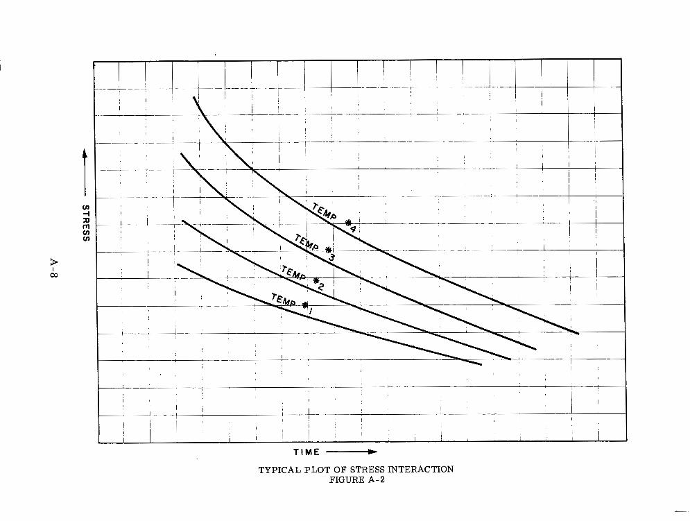
TYPICAL PLOT OF STRESS INTERACTION FIGURE A-2

where
D = degradation of the unit
t = time
Another model is available which relates the fatigue of meter parts with the number of stress cycles applied to the parts. This differs from the above equation in that the plot of s t ress vs. number of cycles is known to be asymptotic. That is, below a particular stress no failure will oc- cur even though the stress were to be applied an infinite number of times. The study of any stress-producing metallic fatigue will be de- signed to reveal this asymptote s o that it wil l be known when the s t ress applied during an actual flight exceeds this amount.
If this study shows that it is valid to assume that the effect of s t ress is cumulative and degrades the part in a known manner before failure oc- curs, a plot of acceleration factors can be made. If the effect of s t ress on part degradation is linear, this plot can be made in the following manner.
a. From the previously obtained plot of s t ress vs. life, find the life at the minimum anticipated s t ress (LM)
b. From the same plot, list life at a number of different s t ress levels (L,)
c. Calculate the acceleration factor (A) for each stress level according to the equation:
L M A = -
d. Plot the points obtained in c. on a graph of s t ress vs. accele- ration factor.
This procedure wi l l produce a curve similar to that shown in Figure A-3. From this information, an estimate can be made of the expected life under any mission profile. The mission can be broken into various seg- ments such as prelaunch, boost, orbit, re-entry, etc. , each of which has a set of constant stresses. The time the unit is subjected to each stress multiplied by the acceleration factor is equivalent to a certain time under minimum s t ress conditions. By adding up each of these time
A-9

ACCELERATION FACTOR
;P m r
TYPICAL ACCELERATION CURVE FIGURE A-3
segments, the equivalent operating time under minimum s t ress condi- tions can be obtained. Comparing this to the mean time to failure for minimum s t ress conditions, the probability of a successful mission can be obtained.
The information obtained in this study can easily be extended to almost any digital microelectronic system. The sample units were selected to include all of the basic building blocks of a typical system. To apply the information obtained in this study, determine how many of each of these blocks are present in the system then, if exponential failure rates are assumed, add up the failure rates for each of these blocks. If the failure rate is known to be non-exponential, other methods a re avail- able to determine the failure rate of the system.
Because of cost considerations, only the environments and combinations of environments felt to be most important were included in this study. Much more information can be obtained during this program if more samples are used to study additional s t ress interactions.
A3 DESCRIPTION ___ OF SAMPLE
A generalized block diagram of the test sample unit to be considered for this reliability program is shown in Figure A-4. It is designed to include all the functions normally used in a digital control system and to exercise the logic elements in a manner duplicating system operation.
The sample unit consists of a serial adder, two shift registers, and a number of transfer gates.
Operation of a sample unit would be as follows:
A data word, numerically equal to one, would shift, serially, into shift register Number 1. By parallel transfer, data from shift register Number 1 would be entered into shift register Number 2. Both registers now contain the same data.
A new data word, equal to one, enters the adder and, due to the recirculation loop, is added to the previous content of shift re- gister Number 1. During this same shift data from register Number 2 is subtracted from the initial data in register Num- ber 1. If a difference occurs, failure is indicated and a fail- ure alarm flip-flop is set. If no error has occurred, the cycle continues with register content increasing by one, each word time. When an overflow occurs, the registers are set to zero and the entire program repeats.
A-11

r - - - - - - - - - -1 I
sc
CLOCK - INDEX SA N S1A-t COUNTER RS
GATES INHIBIT CLOCK TO THIS SECTION AND ANNUNCIATE
N STAQE SHIFT REG%
LEGEND DATA WORD I
DW = DATA WORD L"- I I
I" -l FF = FLIP -FLOP I I '[{d I INHIBIT = FA1 PAIR LURE CLOCK OF } RS = RESET PULSE
I
SECTIONS I I
F""-J IS S I YULATOR SECTIONS AND RS ANNUNCIATE
ALARY I
SA = SERIAL ADDER I I
's SC = SHIFT COMB 1 SS = SERIAL SUBTRACTOR
TFR= TRANSFER PULSE h3 I
I I TYPICAL SYSTEM 1 FUNCTIONAL SECTION
I I
LIFE TEST ASSEMBLY L "" I """"- 1
I I r """ 1"- I I I DW
I I I
I
"""
INHIBIT CLOCK TO THIS SECTlOll AND ANNUNCIATE
I 1 SAMPLE UNIT BLOCK DIAGRAM - DIGITAL SYSTEM RELIABILITY TEST
FIGURE A- 4

All sample units under test, even though each is undergoing a different test, get the same data word at the same time, shift in synchronism, and transfer data at the same time. All re- gisters, then, should contain the same number at the end of any word time.
Failure detection within a unit has been described above. The same method would be used to detect differences between any one unit and another. The comparison could be cascaded to cover all possible combinations, although this appears to be impractical.
Failure is thus defined as erroneous data in any one or more registers at the end of any word time.
Each unit, under test, would be provided with individual elapsed time indicators. In event of failure the fail indicate flip-flop would stop the faulty unit, or units, and the associated elapsed time indicator (s) . Indicator lights on all registers and fail flip-flops could be used for fault location and correction.
All indicators, serial subtractors, fail flip-flops, master clock index counter, and distribution matrix would be remote from the test environment.
A4 SUMMARY
Consideration of various approaches to reliability testing of digital systems leads to the conclusion that step-stress methods offer the greatest opportunity for obtaining meaningful results in the least amount of time and at minimum cost. A reasonable means of select- ing a test sample has been determined which may be applied to the majority of digital systems.
Certain assumptions have been made with regard to the application of step-stress testing for which no rigorous justification can be found within the state-of-the-art. This is particularly true in the area of extrapolation of short-time data to long-time operation through the derivation of acceleration factors. Further study is required to establish confidence in such a hypothesis. The advantages of the step-stress method, however, clearly warrant such continued study to either prove or disprove the theory.
A-13

APPENDIX B
GENERAL DESIGN PROCEDURE
FOR
SPACECRAFT CONTROL SYSTEMS
B- 1
.

APPENDIX B
GENERAL DESIGN PROCEDURE FOR
SPACECRAFT CONTROL SYSTEMS
B1 DESIGN TECHNIQUE
The following is a description of a design technique that applies to any linear, stationary sampled system. A reaction-wheel controlled spacecraft simulator is used as an example of the technique. While this technique can be applied to a controller such as was built under contract NASw 1004, it has been expanded here for the more general case of proportional plus integral plus rate control.
B2 PLANT MODEL
The system is divided into two parts -- the plant and the controller, (see Figure B-1). The plant is defined a s that part of the system which cannot or will not be altered during the design. The object, then, is to design a controller that provides the best control of the plant according to some specified criteria.
The first step in the design procedure is to obtain the normal form (State Model) of the plant (see References 6 and 7). For this design procedure, it will be assumed that the output of the plant is a state variable and that the plant inputs are separated into control and dis- turbance inputs.
The general form of the state model will then be:
where
zp (t) = an n dimensional vector
A ,, E,, - u p = constant matrices
r = the plant input that will be supplied by the con- -, troller, and
B-2

A/D CONVERTER
DIGITAL CONTROLLER
GENERAL MODEL OF SAMPLED SYSTEM FIGURE B- 1
B-3

- F (t) = the external disturbance.
The spacecraft, the reaction wheel and motor, and the amplifier are defined as the plant. The made1 is obtained as follows:
Reaction Wheel: dWW L W - - - - Eq. B-2 dt IW
Eq. B-3
Torque Motor: Lln = BW, + KV6 Eq. B-4
reaction wheel velocity
reaction wheel torque
reaction wheel inertia
0.367 (lo4) gm-cm2
spacecraft velocity
spacecraft torque
spacecraft inertia
0.333 (IO*) gm-cm2
motor torque
damping
25.32 dyne-cm/rad/sec
gain (including amplifier)
0. 424 (lo6) dyne-cm/volt
amplifier input
B-4
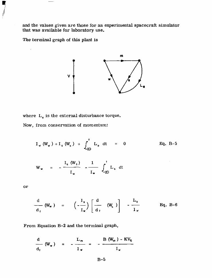
and the values given are those for an experimental spacecraft simulator that was available for laboratory use.
The terminal graph of this plant is
m
11 where Le is the external disturbance torque.
Now, from conservation of momentum:
Eq. B-5
or
From Equation B-2 and the terminal graph,
B-5

and with the approximation that W, M W, ,
From Equations B-6 and B-7
or
Eq. B-8a
Let
Eq. B-8b
B-6

where
8, = spacecraft position
Thus, Equations B-8a and B-9 may be written as
-
-a 0
1 0
d
+
which is in the form required by Equation B-1.
B3 DISCRETE PLANT MODEL
K
IS -
0
v6 +
Eq. B-9
The continuous plant model is next converted to a system of linear difference equations that provide information only at the sampling instants.
The general solution to Equation B-1, subject to the initial conditions,
B-7

and that
E (T) = Et and r (T) = r for to 5 e t 0
- +O
can be written as
where 2 2 3
A p & t o ) AP (t - t o ) A (t- t0)3 e = u + AP ( t - to ) + + - - + . .
2 1 3 1
. . . + + ...... n !
A , @ - t o ) The matrix, e- and the convolution integral of Equation B - l l can be evaluated by functions of matrices (see Reference 8). The general form of the results are given by the vector equation
- X (k + 1) = " A i X, (k) + " Bi r (k) + U: F (k) Eq. B-12a "
where
- X (k) = X
- r (k) = r " 0
"t 0
- F (k) = - Ffo
- X(k+l) = X - ( t o + h )
h = the sampling period.
B-8

Replacing k by k-1 in Equation B-12a gives
- X , (k) = A*, X , (k-1) +B: " r (k-l) = F (k-1) . Eq. B-12b -
For the particular plant given in Equation B-10, the eigenvalues of& are determined as the roots of the following equation.
or
x ( h + Q ) 0
From Equation B-13, the eigenvalues are determined as
Therefore,
where ,, and z ,, are constituent matrices.
Let
then
Eq. B-13
Eq. B-14

and solving 'for E , , gives
1 - a + a 0 Z - -
- 1 1 x, - x 2
1
Eq. B-15
Since z,, +z2, = U - (see Reference 61,
Therefore,
and
B-10

Withr (T) and F (T) constant for to ~ T c t and with t = to + h, Equation B-11 can be written as
- X ( t , + h ) = ( Z I I + z21 e- ' ) Zt, + Eq. B
- Q h
the difference equations describing the plant given in Equation B-10 are written as
{I,
16
{ [ :] V6 (k-1) + [ -11 f ( k - 1 4
B-11
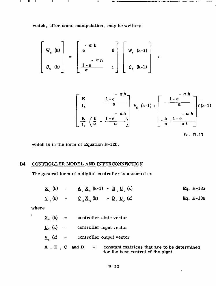
I 111 I I I
which, after some manipulation, may be written:
- a h 1 - e
a
- a h 1: (; - l - e Q 1 V6 (k-1) +
- - a h 1 - e -
a
- Q h - - h + l - e
Q a2
f (k-1)
c
Q. B-17
which is in the form of Equation B-12b.
B4 CONTROLLER MODEL AND INTERCONNECTION
The general form of a digital controller is assumed as
= A C xc (k-1) + - B c u c (k)
= C X (k) + D U (k) - C - - c - c
- - controller state vector
= controller input vector
- - controller output vector
Eq. B-18a
Eq. B-18b
A , B , C and D = constant matrices that are to be determined for the best control of the plant.
B-12

As can be seen from the model, the controller storage (state) 3, (k) is determined by a linear combination of the previous storage (state) and the present inputs. It is assumed that the controller and plant will be interconnected in the feedback configuration of Figure B-2. Thus,
For the plant given in B-17, the simplest controller that provides proportional, rate and integral control is selected. The state model of this controller is
Eq. B-19a
Q. B-19b
where
X, (k) = the content of a storage register
P, , P2, P3, and P4 = constants to be determined
U , (k) and U, (k) = inputs
With E = 0, Figure B-2 provides
The matrices of Equation B-18 are
A = 1 'C
B - C = [P4 P3]
Q. B-20a
Eq. B-20b
B-13

I
PLANT
SYSTEM INTERCONNECTION DIAGRAM FIGURE B-2
cc = 1
D -c = [ P I p2]
With the conditions
Equations B-12b and B-18 may be written as
Eq. B - 2 0 ~
Eq. B-20d
Eq. B-21
Eq. B-22
Eq. B-23
Eq. B-24

Substituting Equation B-24 into B-22 gives
Writing Equations B-23 and B-25 in matrix form
Eq. B-26
Since
then
Eq. B-27
B-15

From Equation B-17
"p A* =Ie- '1 - a h 11 =, 11 1 - e
AP21 -
From Equation B-17
- Q h 1 - e
Q 1
- a h
-P u* = I a
- Q h
and since
_Ac = 1
cc = 1
B-16

then
Eq. B-28
B-17

B6 OPTIMIZATION
The design objective is to determine the controller parameters, that is to say the values of PI , P2 , P3 , and P4 , which will produce mini- mum pointing error for a specified expenditure of energy (cost),given that the plant disturbance is of a particular form, i. e. ,
ERROR = minimum
COST = specified energy
This problem can be viewed as a conventional Lagrange Multiplier problem in which the function
Q = ERROR + W (COST)
is minimized. Normally the Lagrange Multiplier, W, is determined from the partial derivatives of Q with respect to the parameters along with the constraint equations. In this procedure, however, W is treated as a pre-assigned weight and Q is minimized with respect to the con- troller parameters by a one-dimensional computer search. With the particular parameters that minimize Q, both e r ro r and cost are numeri- cally evaluated. If the specified cost is then considered as the computed value of cost, the value of error will then be minimum with respect to the controller parameters subject to the specified cost constraint. The process is repeated for many values of W and a trade-off curve of error versus minimum cost is generated.
To prepare a computer program the spacecraft error function was selected as
a2 1 1 spacecraft pointing error I dt
0
with the integral being approximated by the trapezoidal rule. The cost function was selected as
a3 / Ispacecraft and acceleration I dt 0
B-18

because of the apparent relationship between acceleration and integrated power (energy). This latter integral was approximated by the rectangu- lar rule. The integral approximations are made over a sufficiently long, though finite, time to assure good accuracy. The external disturbance was assumed to be a torque impuke of 105 dyne-cm-sec applied to the laboratory spacecraft simulator immediately after a sampling instant. This "worst case" condition is accounted for by the proper specification of the spacecraft initial conditions,
-10
and
h
where the initial position, 8 (to), is equal to the initial pointing e r ror by the conditions of Equation B-21. Also from Equation B-8b
B (lo5)
I s 1, f (t) = f (k) = a constant =
During early tests of the computer program parameter P4 was found to have little effect on the trade-off curve and hence it was set to zero. It should be noted that, with reference to a physical controller, the parameters P, , P2, and P, represent integrator gain, rate gain and proportional gain, respectively.
Figure B-3 shows a resulting family of trade-off curves for various sample periods. A listing of the computer program which generates these curves is given in Figure B-4.
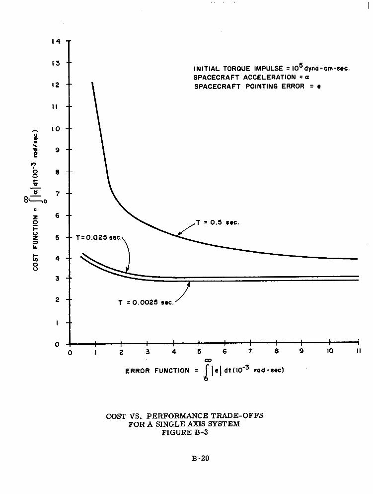
I NlTlAL TORQUE IMPULSE = IO5 dyna - cm-sec. SPACECRAFT ACCELERATION = a SPACECRAFT POINTING ERROR = e
T = 0.5 sac.
T = 0.025 sac.
T = 0.0025 sac.
I I I 1 I I I I I L I I I I 1 I I I I I I I 0 I 2 3 4 5 6 7 8 9 IO II
ERROR FUNCTION = e l d?(10'3 rad -sac)
I I I 1 I I I I I L I I I I 1 I I I I I I I 0 I 2 3 4 5 6 7 8 9 IO II
ERROR FUNCTION = e l d?(10'3 rad -sac)
COST VS. PERFORMANCE TRADE-OFFS FOR A SINGLE AXIS SYSTEM
FIGURE B-3
B-20

ZZJOB 5012 Z Z F O R X C D I G I T A L C O N T R O L L E R O P T I M I Z A T I O N PROGRAlYl
D I M E N S I O N P ~ 1 0 ~ * P I N C ~ 1 0 ~ r X ~ 1 0 ~ r ~ X ~ l ~ ~ ~ A ~ l O ~ l O ) ~ B ~ ~ O ) r C ~ ~ O ~ r S ( ~ O ~ 1 * W W X ( 1 0 ) * E P ( 2 0 ) r C P ( 2 0 )
2 F O R M A T ( I X I I B H I N I T I A L P A R A M E T E H S * ~ X I ~ ~ H ~ ~ I T I A L P A R A I w E T t H I N C H E M k N T ) 3 F O R M A T ( 7 X r E 1 0 . 3 r l i ’ X ~ E l O ~ 3 ) 4 F O R M A T 5 F O R M A T 6 F O R M A T 7 F O R M A T 8 F O R M A T 9 F O R M A T
10 F O R M A T 1 1 F O R M A T 1 2 F O R M A T 13 F O R M A T 14 F O R M A T 1 5 F O R M A T 1 6 F O R M A T 1 8 F O R M A T 19 F O R M A T 20 F O R M A T
1 1 0 F O R M A T C A L L C
2 1
1 7 60
25
26
1 0 0 1 0 1 27
28 29
/ / / * 1 4 X * B H W E I G H T = r E l O . 3 r / ) /// 1 l X r 1 4 H I N I T I A L C O S T =rE10.3) l X r 1 5 H I N I T I A L E R R O L ? = r E 1 0 . 3 . / / ) / r l X r l l H I N I T I A L 0 =rE10.3) l X r 2 H Q = r E 1 0 . 3 ) 7 X r l O H P A R A M E T E R S r l B X . 9 H T O L E R A N C E ) / / / r l X * 1 9 H F I N A L V A L U E S F O R W = . E 1 0 . 3 . / ) 1 X r 6 H C O S T = r E 1 0 . 3 ) I X r 7 H E R R O R = r E 1 0 . 3 * / / ) 1 6 1 5 ) 8E10.3) l X . 7 H W E I G H T = . E 1 0 . 3 ) I X . 1 6 H N U M I S T O O S M A L L ) 3 4 X . 3 H H = r E 1 0 . 3 r / / ) 8 E 1 0 . 3 ) 2 5 X l B H S A M P L I N C P E R I O D = E10.3) N T E R
(
(
(
(
(
(
(
(
(
(
(
(
(
(
(
(
(
E C A L L D A T E C A L L C E N T E R R E A D l S r W r W D I V * W M I N . H . D A M P ~ W I ~ G A I N . S I ~ R E A D 1 5 r N O R D r N P A R r N D I V * N U I V I * I S T O P
K Z = 1 R E A D 1 5 r ( P ( I ) r I = l r N P A R ) R E A D 1 5 r ( P I N C ( I ) r I = l r N P A R ) P U N C H 1 9 r H P U N C H 1 1 0 HEFF C A L L C E N T E R D O 1 7 JJ=l r N P A R C ( J J ) = O . S ( J J ) = P I N C ( J J ) K K = 1 GO T O 200 P U N C H 4 . W P U N C H 2 D O 26 I = 1 r N P A R P U N C H ~ * P ( I ) * P I N C ( I ) P U N C H 4 r W C O S T = H * C S T E R R O R = H * E R R Q M I N = Q T E S T P U N C H B r Q M I N P U N C H 6 r C O S T P U N C H 7 r E R R O R D O 39 K= 1 r N D I V D O 4 3 I= 1 r N P A R P ( I ) = P ( I ) + P I N C ( I ) KK=2 GO T O 201 IF ( Q T E S T - Q M I N ) 29.30.30 O h l l N = Q T E S T C O S T = H + C S T E R R O R = H + E R R
I P U L S E . HEFF
DIGITAL CONTROLLER OPTIMIZATION PROGRAM FIGURE B-4 (1 of 3)
B-21
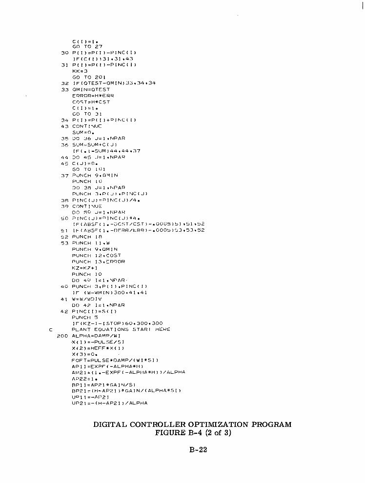
C ( I ) = I . GO T O 27
30 P ( I ) = P ( I ) - P I N C ( l ) I F ( C ( 1 ) ) 3 1 * 3 1 * 4 3
3 1 P ( I ) = P ( I ) - P I N C ( I ) K K = 3 GO T O 2 0 1
32 I F ( Q T E S T - Q M I N ) 3 3 * 3 4 * 3 4 33 Q M I N = Q T E S T
E R R O R = H + E R R C O S T = H + C S T C ( I ) = 1 . GO TO 31
34 P ( I ) = P ( I ) + P I N C ( I ) 4 3 C O N T I NUE
SUM=O. 35 DO 36 J= 1 N P A R 36 SUM=SUM+C ( J 1
I F ( . l - S U M ) 4 4 * 4 4 * 3 7 44 DO 4 5 J = l r N P A Q 4 5 C ( J ) = O m
GO T O 1 0 1 37 P U N C H Y r Q M I N
P U N C H 1 0 D O 38 J= 1 * N P A R P U N C H 3 * P ( J ) r P I N C ( J )
3 A P I N C ( J ) = P I N C ( J ) / 4 . 39 C O N T I N U E
D O 50 J=l * t \ j P A R 50 P I N C ( J ) = P I N C ( J ) * 4 .
IF(A@SF(1.-~CST/CST)-.00~5)51*~1*52 5 1 I F ( A H S F ( l . - D E R R / E R ~ ) - . 0 0 0 5 ) 5 3 * 5 3 * ~ 2 52 P U N C H 1 8 53 P ~ J N C H 1 1 .W
P U N C H 9 . Q M I N P U N C H 1 2 * C O S T P U N C H 13 * E R R O R K Z = K Z + 1 P U N C H 1 0 D O 4i) I = l * N P A R -
40 P U N C H 3 * P ( I ) e P I N C ( I ) IF ( W - W M I N ) 3 0 0 * 4 1 * 4 1
4 1 W=W/WDIV D O 42 I = I o N P A R
42 P I N C ( I ) = S ( I ) P U N C H 5 IF(KZ-l-ISTOP)60r300*300
C P L A N T E Q U A T I O N S S T A R T H E R E 200 A L P H A = D A M P / W I
x ( 1 1 = - P U L S E / S I X ( E ) = H E F F * X ( 1 ) X ( 3 ) = 0 . F O F T = P U L S E + D A M P / ( W I * S I ) A P l l = E X P F ( - A L P H A * H ) A P 2 1 = ( 1 . - E X P F ( - A L P H A * H ) ) / A L P H A A P 2 2 = 1 R P l I = A P 2 I + G A I N / S I B P 2 1 = ( H - A P 2 1 ) * G A I N / ( A L P H A * S l ) U P I I = - A P E l U P 2 1 = - ( H - A P 2 1 ) / A L P H A
DIGITAL CONTROLLER OPTIMIZATION PROGRAM FIGURE B-4 (2 of 3)
B-22

C P L A N T E Q U A T I O N S END A N D S Y S T E M E Q U A T I O N S S T A R T HERE 2 0 1 A ( l r l ) = A P I I - B P I l * P ( I )
A ( 1 * 2 ) = - B P l l * P ( 2 ) A ( 1 r 3 ) = B P 1 1 A ( 2 r l ) = A P 2 1 - f 3 P 2 1 * P ( 1 ) A ( 2 r 2 ) = 1 . - B P 2 1 * P ( 2 1 A ( 2 * 3 ) = B P 2 1 A ( 3 r l ) = - P ( 3 ) * A P 2 1 + P ( I ) * D ( 3 ) * B P 2 1 A ( 3 , 2 ) = - P ( 3 ) + P ( 2 ) * P ( 3 ) * ~ P 2 1 A ( 3 . 3 ) = 1 . - P ( 3 ) * U P 2 1 8 ( 1 ) = U P l l * F O F T 8 ( 2 ) = U P E I * F O F T B ( 3 ) = - P ( 3 ) * U P 2 1 * F O F T D O 202 I I = l r N O R D
202 w x ( I I ) = x ( I I ) CST=O. ERR=O. BETA=(GAIN*P(l)/SI)+ALPHA D E L T A = G A I N * P ( 2 ) / 5 1 G A M M A = G A I N / S I ACC=-BETA+'WX( 1 ) - D E L T A + W X ( 2 ) + G A l ~ i M A * W X ( 3 ) - F O F T C S T = A B S F ( A C C ) D O 205 LL= 1 .NUM D W X 2 = W X ( 2 ) DO 206 I I = 1 r N O R D
206 W W X ( I I ) = O . D O 203 I I = 1 .TdORO D O 203 JJ= 1 r N O R D
203 W W X ( I I ) = W W X ( I I ) + A ( I I * J J ) P W X ( J J ) D O 2 ~ 4 I I = 1 *N0;7D
2(?4 WX( I I ) = W W X ( I I ) + H I I 1 ) D E R R = E R R D C S T = C S T A C C = - H t T A * W X ( 1 ) - I>ELTA*WX ( 2 +GAl"lViA*WX( 3 ) "FUf; T L R R = E R R + A H S F ( ( U W X Z + d X ( Z ) ) / 2 . ) C S T = C S T + A t j S F ( A C C )
C S Y S T E M E Q U A T I O N S END H E H L 205 C D N T I N U E
O T F S T = H * t R R + d + H * C S T GO T O 1 2 5 . 2 8 * 3 E ) . K K
300 C A L L E X 1 T ENU
* D A T A O P T I M I Z A T I O N - S P A C t C H A F T CUNT+!OL S Y S T t i 4
40. 2. 625 .5 1 onooo. .no25 3. 3. 4. 90.
1 0 . 2. .3 1 5 8 . 7 8.1 1 2 1 6 9 8
z z z z
25.32 3670.
7 .
DIGITAL CONTROLLER OPTIMIZATION PROGRAM FIGURE B-4 (3 of 3)
B-23

APPENDIX C
COMPUTER PROGRAM DATA
0 Program Listing 0 Program Flow Chart 0 Program Description 0 Program Symbol Table
c-1

APPENDIX C
COMPUTER PROGRAM DATA
C1 STATE MODEL COMPUTER PROGRAM
The state model of the system developed for this study contract was programmed for an IBM 1620 computer using FORTRAN II-D language. This particular computer is rather slow and a review of the program flow chart (Figure A-1) will show that a great amount of computation time was saved by using logical decisions to implement all saturation functions instead of calculating these functions directly.
Numerical integration is carried out by use of a fourth order Runge- Kutta technique which integrates in discrete steps. This method has the advantage that no special computations are needed to start the solution and the e r ro r is of the order of h5, where h is the interval of integration. Consider the equation
then the increment for advancing the dependent variable can be found from:
Y = 1/6 (k, + 2 k, + 2 k 3 + k4)
where
k, = h f (x, + h/2, yo + k, /2)
k 3 = h f (x, + h/2, yo + k2/2) k, = h f ( x o + h, yo + k3).
Now, setting x , = x, + h and y I = yo + n y the process is repeated as required. The program version of this technique can be found in the listing (Figure C-1) beginning at statement 100 and continuing through statement 112. Temporary working values of the state variable ( X W ) are initialized in statements 5 and 6.
c-2

Provision was made in this program to vary the interval of integration (h = DT) so that transient output of the. rate network could be ob- served. In statements 200, 402 and 403 a test is made of the rate of change of voltage across the lead network capacitor and if the slope is greater than a specified value (DVC) the interval of integration is di- vided by 10. The interval is set back to its normal value as soon as DXDT (5) is less than the test value.
This program was written directly from the block diagram of Figure 6 in the Section 2-3 of this report. Comparison of the program flow chart with this block diagram wil l show the correspondence. Because of certain limitations placed on the use of characters in the FORTRAN language, however, certain variable symbols used in the block dia- gram do not appear explicitly in the computer program. A complete listing of the program variables and their definitions appears in Table c-1. Although this program applies to a specific system and is therefore not of general use the state variable model has proved to be a powerful tool in systems design and analysis. The technique can readily be ap- plied to any systems problem for which a state model can be prepared.
TABLE C-1 PROGRAM SYMBOL TABLE
Page 1 of 4
Program Variables
CE
CD
CI
CR
CG
CDA
R1
Definition
Encoder gain, bits/radian
Damping register multiplier
Integrator gain, seconds
Rate multiplier gain, pulses/bit
Reaction where gain, pulses/radian
D/A converter gain, volts/bit
Lead net series resistor, ohms
c- 3

Page 2 of 4
Program Variables
R2
CAP
cc SI
X(I), I = 1 , 2 . . . 6
WI
T
TI
THC
TQE
RATE
TSMP
DVC
DPR
N
PR
NPG
NPX
I
MTHl
Definition
Lead net shunt resistor, ohms
Lead net capacitor, farads
Chopper gain, 1 / 2 6
Spacecraft inertia, gm-cm 2
State variables
Wheel inertia, gm-cm2
Real time, seconds
Test increment, used to assure that integrator will not sample until error value has been tested
e,, Spacecraft position, radians
External disturbance torque, dyne- cm
Sampling rate set point, seconds
dt accummulator
Runge-Kutta variable increment switch
Output print interval control
Number of state vector calculations
Output print counter
Output page number
Page line counter
Index variable
Largest integer value in spacecraft position data. This is used to simu- late real encoder data since fractional values are not available.
c-4

Page 3 of 4
Program Variables
TH1
TJET
L
JET
TDUMP
DI
INC
TH5
PRA
v7
sv TL
J
DEGI
DEG3
xw
H
K
K2
Tw M
Definition
Floating point value of MTHl
Jet torque, for momentum dumping
Runge-Kutta flag
J e t on-off indicator
Dump offset correction torque
Time increment
Runge-Kutta variable increment f l a g
Sum of proportional and integrator register contents
PRF of rate multiplier
Lead network output
Sign flag for V6
Load torque
Index variable
Spacecraft velocity, degrees/sec
Spacecraft position, degrees
Runge-Kutta working value of state variables
Interval of integration, equal to DT
Index variable
Index variable
Runge-Kutta working value for time
Index variable
c- 5

Page 4 of 4
Program Variables
M2
TH2
TH4
TH6
PRB
S6
V6
TS
IRPS
Definition
Index variable
Error data input to proportional and integrator registers
Proportional register content
Buffer register content
PRF of reaction wheel quantizer
Speed control saturation flag
Amplifier input
Stall torque
Reaction wheel velocity, RPS
C6

(-) PR.0 NPG.1
PUNCH PAGE NO.
PUNCH
MTHl =CE* X(3) T H l = MTHl K = 1 K 2 = 1 TJET=WIXCR*48.8/CG L = I TWmT JET= 0 TI)MP= 0
INC.2
c, M2.4
+ OXDT( 5)>0VC
Q INC= {
MTHl'CEXX(3) THl: MTHl MTHl'CEXX(3) THl: MTHl
NOTE: NUMBERS ON CHART ARE STATEMENT NUMBERS.
TH2 = TH! -THC
-+ TH7.5-64
Q" K2.1
SYSTEM MODEL COMPUTER PROGRAM FLOW CHART FIGURE C-1 (1 of 6)

3 XI4E64.HCDA
X(41564.HCDA
i"l, , ,373 1 , r, K.2 K=3
r -9 X(41264.YCDA
399
8 Q
381
=+TJET CT=4 (= 3 2.2
TDUMP. -T JET
T DUMPCO. JET=O
K2.1
SYSTEM MODEL COMPUTER PROGRAM FLOW CHART FIGURE C-1 (2 of 6)

3 8 7
1 1 b DXDTW= -48.8
++ TH2 2 1024.
0
4
Q
19 . 21 2 2 . TH4 = 4095. TH4=CDNTA2 TH4=-4095.
SYSTEM MODEL COMPUTER PROGRAM FLOW CHART FIGURE C-1 (3 of 6)

T- Y
3 3
S6. t 1
4 . 6
D X D T ( 4 ) = S 6 * C D A * ( P R A - P R B ) D X D T ( 5 1 = [ X ( 4 ) / R 2 - X ( 5 1 3 C ( R l + R 2 1 / ( R I *R2)]/CAP V 7 . X ( 4 ) - X ( 5 1 V 6 = C C X V 7
e V 6 2 . 0 8 5
TS=2.74E+07XSV)CV62-15.8E t07*V63
TS=
TL~TS-25.32*[X12)-X(l l DXDT(1 I=(-TL-TQE-TDUMPj/SI DXDT(21"TL/WI
Q TW+DT*.5
Q 4 INC=2
SYSTEM MODEL COMPUTER PROGRAM FLOW CHART FIGURE C-1 (4 of 6)

END RUNGE-KUTTA
SYSTEM MODEL COMPUTER PROGRAM FLOW CHART FIGURE C-1 (5 of 6)

9
-64 .YCDA
T - T W + D T
P R n P R t 1 T S M P = T S M P + D T
N P X > 5 2
NPG = NPG + 1 N P X = l
PUNCH
HEADINGS
PUNCH RESULTS
8 CONTINUE
SYSTEM MODEL COMPUTER PROGRAM FLOW CHART FIGURE C-1 (6 of 6)

, C D I G I T A L C O N T R O L L E R S Y S T E M M O D E L L S I S I M U L A T O R
D I M E N S I O N X ( 6 ) * X W ( 6 ) r C ( 3 * 6 ) r D X D T ( 6 ) 1 F O R M A T ( ~ X ~ ~ H T I M E I ~ X * ~ H S C V E L . * ~ X I ~ O H I N T E G R A T O R . ~ X . ~ H S C P0S.r
1 4 X r 7 H D / A O U T r 4 X r 6 H A M P I N * 3 X r 3 H J E T r 3 X 3 H W H L ) 2 F O R M A T ( ~ X I ~ H S E C . ~ ~ X ~ ~ H D E G / S E C * ~ X ~ ~ H ~ I T S * ~ X ~ ~ H D E G ~ ~ X * ~ H V D C ~ ~ X ~ H V A C
l l O X r 3 H R P S / / ) 3 F O R M A T ( E l O . 4 ) 4 F O R M A T ( I 5 ) 7 F O R M A T ( 4 0 X r 3 0 X s 6 H P A G E 12///)
R E A D ~ * C E ~ C D ~ C I * C R ~ C G I C U A * R ~ ~ R ~ ~ C A P ~ C C * S I ~ W I * X ( ~ ) ~ X ( ~ ) ~ X ( ~ ) ~ X ( ~ ) ~ I X ( ~ ) . X ( ~ ) . T I H * T I . T H C * T ~ ~ * R A T E ~ T S M P ~ ~ V C * ~ P R
5 6
C 200 402 403
4 04
C 405 390
39 1
366 395 396 36 7 368
397 398 399
369 370
R E A D 4 r N PR=O. N P G = 1 N P X = O P U N C H 7 r N P G P U N C H 1 P U N C H 2 DO 6 I = l r 6 x w ( I ) = x ( I ) M T H l = C E * X ( J ) T H 1 = M T H 1 K = 1 K 2 = 1 T J E T = W I + C R * 4 8 . 8 / C G L= 1 T W = T JFTT=O T D M P = O D O 3 V O M = 1 .N
I N C R E M E N T S E L E C T I O N S T A R T S H E R E . DXDT(5)=(X(4)/R2-X(5)*(RI+R2)/(Rl*R2) ) / C A P I F ( D V C - D X D T ( 5 ) + D X D T ( 5 ) ) 4 0 3 * 4 0 3 * 4 0 4 D T = H / l O r L = l I N C = 2 DO 300 M 2 = 1 1 0 GO T O 405 D T = H I N C = 1 I N C R E M E N T S E L E C T I O N S T O P S H E R E IF(TSMP-RATE)391*390*390 M T H 1 = C E * X ( 3 ) T H l = M T H 1 TSrnP=O. T H 2 = T H l - T H C I F ( T H 2 - 6 4 . )366*369r369 1 F ( T H 2 + 6 4 . )369*369*395 GO T O ( 3 9 6 * 3 6 7 ) r K 2 K = 1 I F ( T I - C 1 ) 3 9 7 r 3 6 8 * 3 6 8 T I = O . X ( 6 ) = X ( 6 ) + T H 2 X W ( 6 ) = X ( 6 ) IF(X(4)-64.+CDA)398*398*399 IF(X(4)+64o*CDA)399*399*380 K = 1 GO TO 386 IF(X(4)-64.+CDA+1.E-O4)370~370*371 IF(X(4)+64.+CDA-l.E-O4)371*371*372
SYSTEM MODEL COMPUTER PROGRAM, FORTRAN PROGRAM LISTING
FIGURE C-2 (1 of 4)
C- 13

371 K = l
372 I F ( T H 2 ) 3 7 4 * 3 7 4 * 3 7 3 373 K = 2
GO T O 386
GO T O 386 374 K = 3
GO T O 386 380 IF(X(6)-3072.)382*381*381 38 1 T D M P = + T J E T
J E T = - 1 K = 3 K 2 = 2 GO T O 386
382 IF(X(6)+3072.)383.383.384 3 8 . 7 T n M P z - T J E T
J E T = + l K = 2
GO TO 386 K 2 = 2
384 I F ( X ( 6 ) * X ( 6 ) - 1 0 0 . ) 3 8 ~ , 3 ~ 5 + 3 ~ 6 385 TPMP=O.
K = 1 JET=O K 2 = 1
386 GO T O ( 3 8 7 . 3 8 8 - 3 8 9 ) r K 387 D X D T ( 6 ) = 0 .
GO T O 1 8 388 D X D T ( 6 ) = 4 8 . 8
GO TO 18 389 D X D T ( 6 ) = - 4 B . R
1 6 I F ( 1 0 2 4 . - T H 2 ) 1 9 . 1 9 . 2 0 ' 1 9 T H 4 = 4 0 9 5 .
GO T O 23 20 I F ( T H 2 + 1 0 2 4 . ) 2 1 * 2 1 . 2 2 2 1 T H 4 = - 4 0 9 5 .
GO TO 23 22 T H 4 = C D * T H 2 2 3 T H S = X ( h ) + T H 4
I F ( 4 0 9 5 . - T H 5 ) 2 4 * 2 4 + 2 5 24 T H 6 = 4 0 9 5 .
GO TO 28 25 I F ( 4 0 9 5 . + T H 5 ) 2 6 * 2 6 9 2 7 26 T H 6 = - 4 0 9 5 .
GO T O 28 27 T H 6 = T H 5 28 P R A = C R * T H 6
P R B = C G * X ( 2 ) IF(64.*CDA-X(4))29*29*30
29 X ( 4 ) = + 6 4 . * C D A ! F ( P R A - P R B ) 3 3 * 3 3 * 3 2
3 C IF(64.*CCA+X(4))31.31*33 3 1 X ( 4 ) =-64 .*CDA
I F ( P R A - P R R ) 3 2 * 3 3 * 3 3 32 5 6 = 0 .
G 3 TO 34 37 s 6 = + 1 . 3 4 DXDT(4)=S6*CDA*(PRA-PRB)
DXDT(5)=(X(4)/R2-X(5)*(Rl+R2)/(Rl*R2) ) / C A P V 7 = X ( 4 ) - X ( 5 ) V 6 = C C * V 7
SYSTEM MODEL COMPUTER PROGRAM, FORTRAN PROGRAM LISTING
FIGURE C-2 (2 of 4)
C- 14

I F ( V 6 ) 43.43944 43 S V = - I .
44 S V = + 1 . 45 I F ( . 0 8 5 - V 6 ) 35.35.36 35 T S = 102 -E+03
GO T O 39
GO T O 45
36 I F ( . O 8 5 + V 6 ) 3 7 * 3 7 * 3 8 37 T S = - 1 0 2 . E + 0 3
GO T O 39 38 T S = ~ . ~ ~ E + O ~ * S V * V ~ * V ~ - ~ ~ O ~ E + O ~ * V ~ * V ~ * V ~ 39 T L = T S - 2 5 . 3 2 * ( X ( 2 ) - X ( I ) )
D X D T ( l ) = ( - T L - T Q E - T D M P ) / S I D X D T ( 2 ) = T L / W I D X D T ( 3 ) = X ( 1 )
C R U N G E - K U T T A S T A R T S HERE GO T O ( 1 0 0 . 1 0 2 r 1 0 4 r 1 0 6 ) * L
l C 0 D O 1 0 1 Jzl.6 C ( l r J ) = D X D T ( J ) * D T
1 0 1 X ( J ) = X W ( J ) + C ( l * J ) * . 5 T=TW+DT*.5 L=2 G O T O ( 2 0 0 * 4 0 5 ) * I N C
1 0 2 D O 1 0 3 J = 1 . 6 C ( 2 * J ) = D X D T ( J ) * D T
103 X ( J ) = X W ( J ) + C 1 2 * J ) * . S L=3 GO T O ( . ? 0 0 $ 4 0 5 ) . I N C
1 0 4 D O 105 J z 1 . 6 C ( 3 . J ) = U X D T ( J ) * D T
1 0 5 X ( J ) = X W ( J ) + C ( 3 * J ) T = T W + D T L=4 GO TO ( 2 0 0 r 4 0 5 ) * I N C
1 0 6 D O 1 0 7 Jzl.6 107 D X D T ( J ) = D X D T ( J 1 * D T
D O 1 1 2 1 = 1 * 6 I 1 2 X ( I ) = X W ( I ) + ( C ( L r l ) + 2 . * C ( ~ ~ I ) + 2 * C 3 * l I + D X D T ( l ) ) ~ 6 .
c R U N G E - K U T T A S T O P S HERE IF(64.*CDC-X(4))54*54*55
54 X ( 4 ) = + 6 4 . * C C A GO TO 57
55 I F ( 6 4 . * C D A + X ( 4 ) ) 5 6 . 5 6 . 5 7 56 X ( 4 ) = - 6 4 . * C D A 57 T I = T I + D T
T = T W + D T T S M P = T S M P + D T P P = P R + l . I F ( P R - D P R ) I l l * 1 0 8 ~ 1 O U
108 D E G I = X ( I ) * 1 8 0 . / 3 . 1 4 1 6 I R P S = X ( 2 ) / 6 . 2 8 3 2 D E G 3 = X ( , 3 ) * 1 8 0 . / 3 . 1 4 1 6 N P X = N P X + 1 I F ( N P X - 5 2 ) 1 1 3 ~ 1 1 3 . 1 1 4
1 1 4 N P G = N P G + l N P X = 1 P U N C H 7 e N P G P U N C H 1 P U N C H 2
109 F O R M A T ~ 1 X ~ F 8 ~ 3 ~ I X ~ E 1 O ~ 4 ~ l X ~ E l O ~ 4 ~ I X ~ E l l ~ 5 ~ I X ~ E 9 ~ 3 ~ l X ~ E 9 ~ 3 ~ ~ ~ ~ I Z
SYSTEM MODEL COMPUTER PROGRAM, FORTRAN PROGRAM LISTING
FIGURE C-2 (3 of 4)
C- 15

1 1 3 P U N C H 1 0 9 ~ T ~ D E G 1 ~ X ( 6 ) ~ D E G 3 . X o . V 6 . J E T * l R P S 1 3 x 4 1 4 )
PR=O 1 1 1 DO 1 1 0 ] = l e 6 1 1 0 XW(.I ) = x ( I )
L= 1 TW=T
300 C O N T I N U E END
SYSTEM MODEL COMPUTER PROGRAM, FORTRAN PROGRAM LISTING
FIGURE C-2 (4 Of 4)
C- 16

REFERENCES
1. PHISTER, M. , Jr. : Logical Design of Digital Computers, John Wiley and Sons, Inc. , New York, 1958.
2. KEISTER, W. ; FUTCHIE, A. ; and WASHBURN, S., : The Design of Switching Circuits, D. VanNostrand Co. , Inc. , New York, 1951.
3. LEDLEY, R. , : Digital Computer and Control Engineering, McGraw-Hill Book Co., Inc. , New York, 1960.
4. HOHN, F. , : Applied Boolean Algebra, The Macmillan Co. , hc. , New York, 1960.
5. TOU, J. T. , Modern " Control Theory, McGraw-Hill, 1964.
6. ZADEH, L. A. and DESOER, C. A. , Linear Systems Theory: - The State Space Approach, McGraw-Hill, 1963.
7. KOENIG, H. E. ; KESAVEN, H. D. ; and TOKOD, V. , Analyses of Discrete Physical Systems, Part II, (to be published).
8. FRAME, J. S. , "Matrix Functions and Applications", IEEE Spectrum Vol. 1, No. 3 through No. 7, (March through July 1964).
R- 1

, . . _* ’ “The aeronantical and space activities of the United States shall be
.,/. edge of phenomena in the atmosphere and space. The Administration conducted so as t o contribrrte . . , to the expansiou of hnman knowl-
shall provide for the widest practicable and appropride dissemination of information concerning its activities and the resrrlts thereof.”
“ N A T I O N A L AERONAUTICS AND SPACE ACT OF 1958
.>
NASA SCIENTIFIC AND TECHNICAL PUBLICATIONS
TECHNICAL REPORTS: Scientific and technical information considered important, complete, and a lasting contribution to existing knowledge.
TECHNICAL NOTES: Information less broad in scope but nevertheless of importance as a contribution to existing knowledge.
TECHNICAL MEMORANDUMS: Information receiving limited distri- bution because of preliminary data, security classification, or other reasons.
CONTRACTOR REPORTS: Technical information generated in con- nection with a NASA contract or grant and released under NASA auspices.
TECHNICAL TRANSLATIONS: Information published in a foreign language considered to merit NASA distribution in English.
TECHNICAL REPRINTS: Information derived from NASA activities and initially published in the form of journal articles.
SPECIAL PUBLICATIONS: Information derived from or of value to NASA activities but not necessarily reporting the results .of individual NASA-programmed scientific efforts. Publications include conference proceedings, monographs, data compilations, handbooks, sourcebooks, and special bibliographies.
Details on the availability of these publications may be obtained from:
SCIENTFIC AND TECHNICAL INFORMATION DIVISION
NATIONAL AERONAUTICS AND SPACE ADMINISTRATION
Washington, D.C. 20546