Embed Size (px)
Citation preview

Including random thoughts from David
A Talk on Memory Buffers
2 Inphi Proprietary
2 Inphi Proprietary
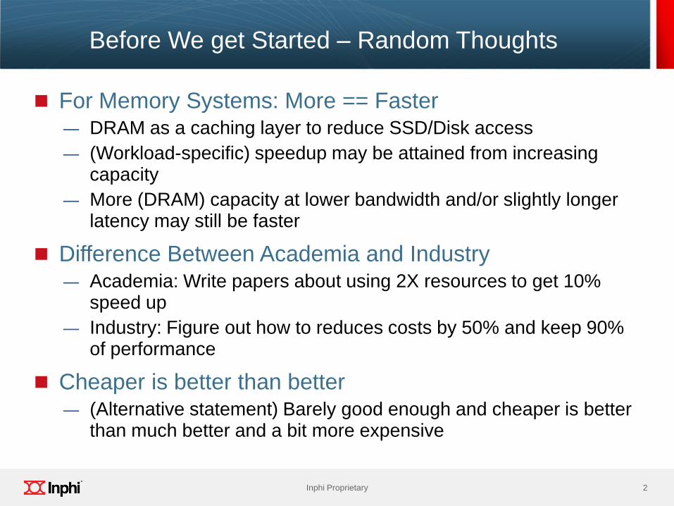
Before We get Started – Random Thoughts
For Memory Systems: More == Faster ― DRAM as a caching layer to reduce SSD/Disk access
― (Workload-specific) speedup may be attained from increasing capacity
― More (DRAM) capacity at lower bandwidth and/or slightly longer latency may still be faster
Difference Between Academia and Industry ― Academia: Write papers about using 2X resources to get 10%
speed up
― Industry: Figure out how to reduces costs by 50% and keep 90% of performance
Cheaper is better than better ― (Alternative statement) Barely good enough and cheaper is better
than much better and a bit more expensive

3 Inphi Proprietary
3 Inphi Proprietary
Quick Historical Review
4 Inphi Proprietary
4 Inphi Proprietary
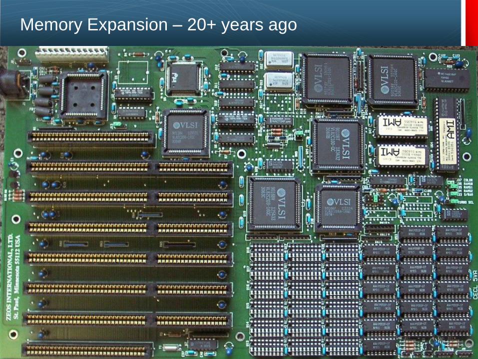
Memory Expansion – 20+ years ago

5 Inphi Proprietary
5 Inphi Proprietary
Then, Memory Modules
6 Inphi Proprietary
6 Inphi Proprietary
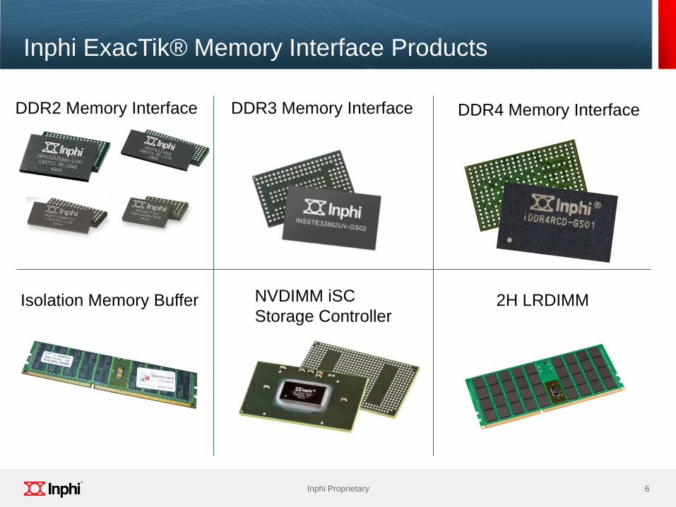
Inphi ExacTik® Memory Interface Products
2H LRDIMM
DDR4 Memory Interface
Isolation Memory Buffer
DDR2 Memory Interface DDR3 Memory Interface
NVDIMM iSC
Storage Controller

7 Inphi Proprietary
7 Inphi Proprietary
Not So Simple Anymore
Memory
Controller Die
Memory
Controller
Package
Trace
MC
Socket
Open
Field
Trace DIMM
Field
Trace
Socket-to-socket trace
DRAM Die
(DQ Interface)
DRAM PKG Wirebond
PCB Trace (RS to DRAM PKG)
DQ RStub
PCB Trace (Connector to RS)
DIMM Connector
PCB Trace (Breakout
on system board)
DIMM 0DIMM 2 DIMM 1
8 Inphi Proprietary
8 Inphi Proprietary
Why Memory Buffering? Benefits of Buffering
9 Inphi Proprietary
9 Inphi Proprietary
Benefits
More Capacity ― One controller to connect to many DRAM devices
More Bandwidth ― Multiple loads (DRAM devices) slow down bus.
― Buffer-and-re-drive cleans up system signal integrity, enabling higher operating data rate
Better RAS ― Buffers can check correctness of commands/data
Additional Logic Interface to do “interesting things”, e.g. ― (Flash-backed, DRAM Access) NVDIMM
― NVRAM-only NVDIMM
10 Inphi Proprietary
10 Inphi Proprietary
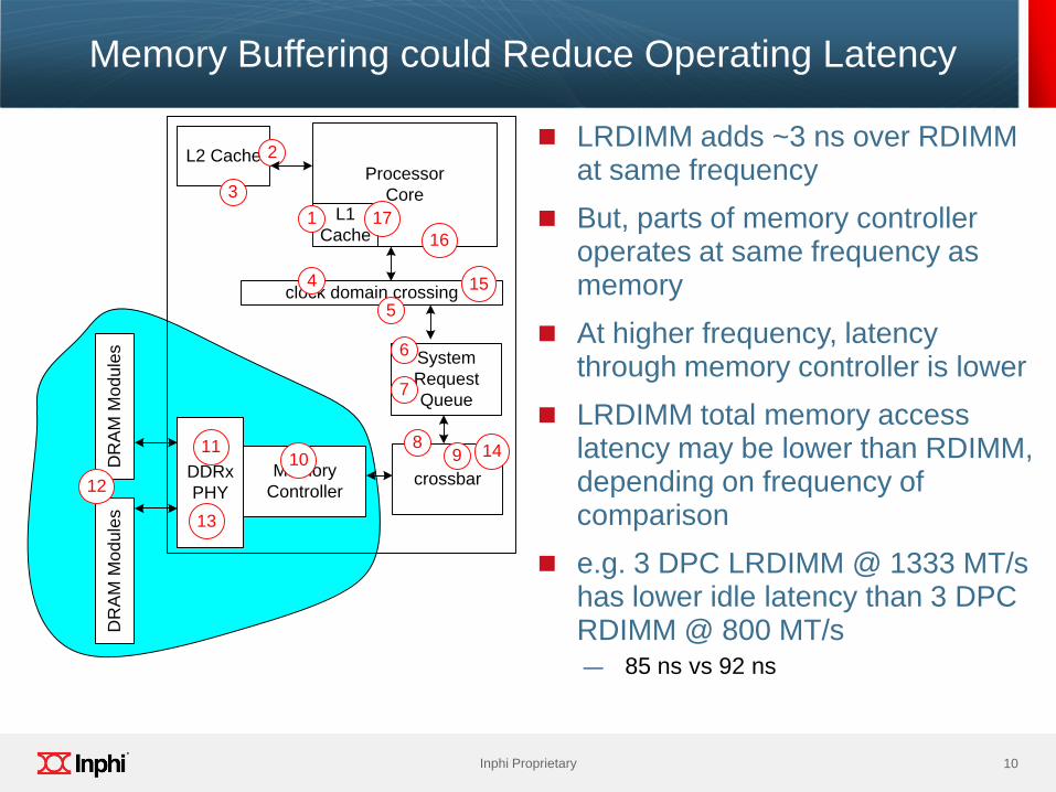
Memory Buffering could Reduce Operating Latency
LRDIMM adds ~3 ns over RDIMM at same frequency
But, parts of memory controller operates at same frequency as memory
At higher frequency, latency through memory controller is lower
LRDIMM total memory access latency may be lower than RDIMM, depending on frequency of comparison
e.g. 3 DPC LRDIMM @ 1333 MT/s has lower idle latency than 3 DPC RDIMM @ 800 MT/s ― 85 ns vs 92 ns
Processor
CoreL1
Cache
L2 Cache
clock domain crossing
System
Request
Queue
crossbarMemory
ControllerDDRx
PHY
DR
AM
Mo
du
les
DR
AM
Mo
du
les
1
2
3
4
5
6
7
8910
11
12
13
14
15
16
17
11 Inphi Proprietary
11 Inphi Proprietary
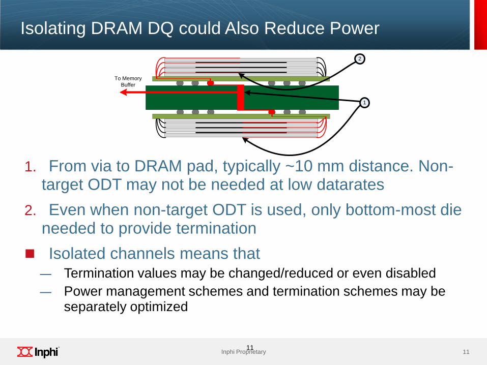
1. From via to DRAM pad, typically ~10 mm distance. Non-target ODT may not be needed at low datarates
2. Even when non-target ODT is used, only bottom-most die needed to provide termination
Isolated channels means that ― Termination values may be changed/reduced or even disabled
― Power management schemes and termination schemes may be separately optimized
11
2
1
To Memory
Buffer
Isolating DRAM DQ could Also Reduce Power

12 Inphi Proprietary
12 Inphi Proprietary
But . . . Memory Buffers should behave and cost like a wire
Zero cost ― Should be tiny and simple to design
Zero latency ― No junk (logic) in data path – logic slows things down
Zero footprint ― DIMM’s and System Board should carry “useful stuff”, not chips
that just buffer and re-drive signals
Zero power ― Ideally . . .
13 Inphi Proprietary
13 Inphi Proprietary
How Do You Build (Architect) a Memory Buffer?
14 Inphi Proprietary
14 Inphi Proprietary
So What Do You Do When you want a Memory Buffer?
Define Scope ― Improve pin-capacity-bandwidth of CPU interface?
― Interface conversion for compatibility
― On-DIMM or On-system-board application
How many pins do you need for this chip or chipset? ― More pins -> Larger package -> higher cost & larger footprint
― Will it fit?
Speed target and power budget
15 Inphi Proprietary
15 Inphi Proprietary
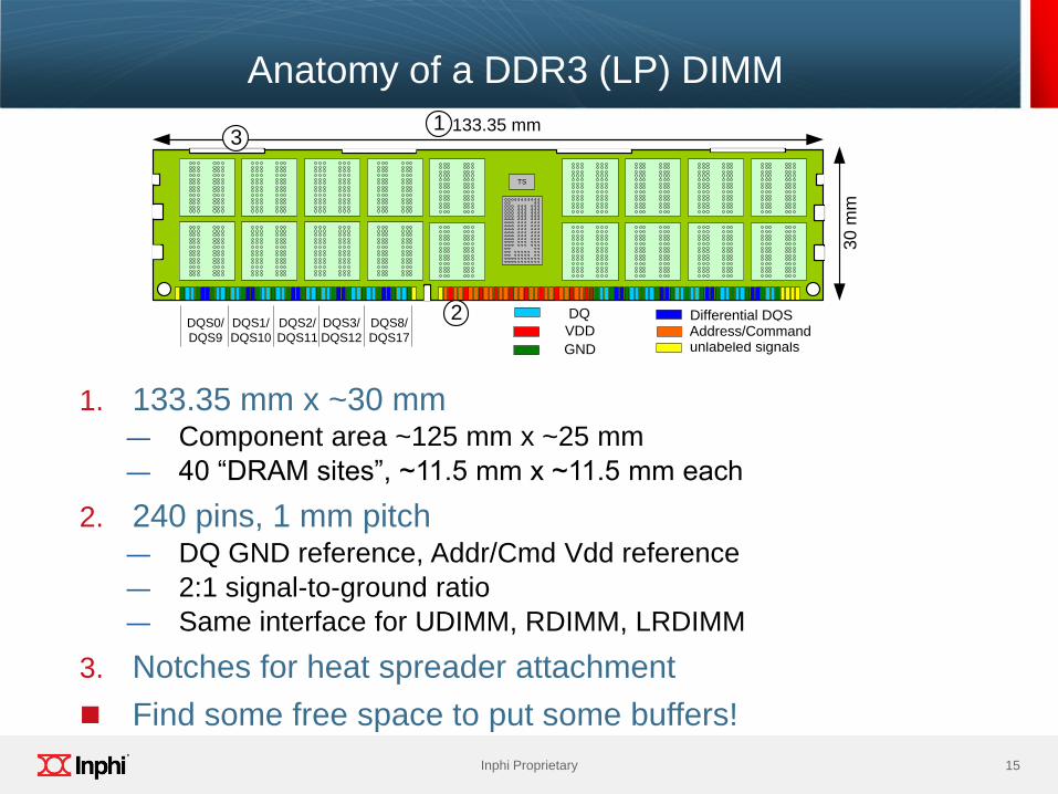
Anatomy of a DDR3 (LP) DIMM
1. 133.35 mm x ~30 mm ― Component area ~125 mm x ~25 mm
― 40 “DRAM sites”, ~11.5 mm x ~11.5 mm each
2. 240 pins, 1 mm pitch ― DQ GND reference, Addr/Cmd Vdd reference
― 2:1 signal-to-ground ratio
― Same interface for UDIMM, RDIMM, LRDIMM
3. Notches for heat spreader attachment
Find some free space to put some buffers!
30
mm
DQS0/
DQS9
Differential DQSDQ
unlabeled signals
DQS1/
DQS10
DQS2/
DQS11
DQS3/
DQS12
DQS8/
DQS17
1
VDD
GND
Address/Command
133.35 mm
2
3
TS
16 Inphi Proprietary
16 Inphi Proprietary
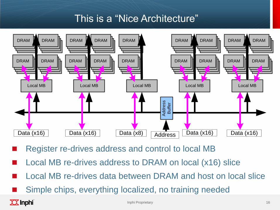
This is a “Nice Architecture”
Register re-drives address and control to local MB
Local MB re-drives address to DRAM on local (x16) slice
Local MB re-drives data between DRAM and host on local slice
Simple chips, everything localized, no training needed
DRAMDRAM
DRAM
DRAMDRAM
DRAM
Local MB
DRAMDRAM
DRAMDRAM
DRAMDRAM
DRAMDRAM
DRAM
DRAM
DRAMDRAM
DRAM
DRAMDRAM
DRAM
Local MB
DRAMDRAM
DRAMDRAM
DRAMDRAM
DRAMDRAM
DRAM
DRAM
DRAMDRAM
DRAM
DRAMDRAM
DRAM
Local MB
DRAMDRAM
DRAMDRAM
DRAMDRAM
DRAMDRAM
DRAM
DRAM
DRAMDRAM
DRAM
DRAMDRAM
DRAM
Local MB
DRAMDRAM
DRAMDRAM
DRAMDRAM
DRAMDRAM
DRAM
DRAM
Local MB
DRAMDRAM
DRAMDRAM
DRAMDRAM
DRAMDRAM
Ad
dre
ss
Bu
ffe
r
AddressData (x16) Data (x8)Data (x16) Data (x16)Data (x16)
17 Inphi Proprietary
17 Inphi Proprietary
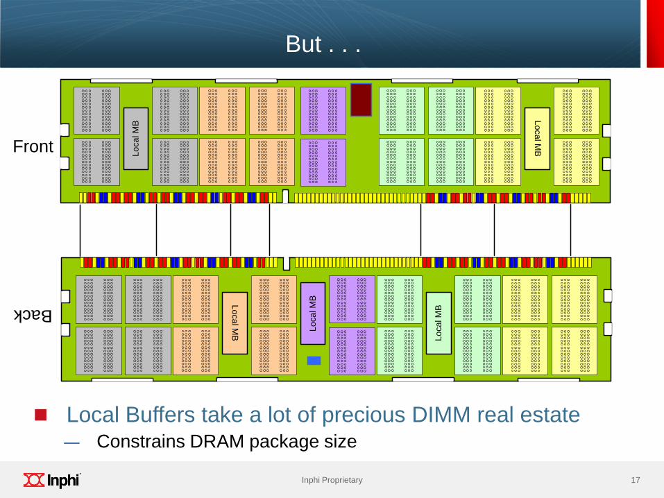
But . . .
Local Buffers take a lot of precious DIMM real estate ― Constrains DRAM package size
Lo
ca
l M
B
Lo
ca
l MB
Lo
ca
l M
B
Lo
ca
l M
B
Lo
ca
l MB
Front
Back
18 Inphi Proprietary
18 Inphi Proprietary
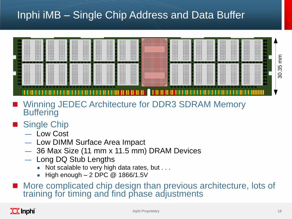
Inphi iMB – Single Chip Address and Data Buffer
Winning JEDEC Architecture for DDR3 SDRAM Memory Buffering
Single Chip ― Low Cost ― Low DIMM Surface Area Impact ― 36 Max Size (11 mm x 11.5 mm) DRAM Devices ― Long DQ Stub Lengths
● Not scalable to very high data rates, but . . . ● High enough – 2 DPC @ 1866/1.5V
More complicated chip design than previous architecture, lots of training for timing and find phase adjustments
30
.35
mm
19 Inphi Proprietary
19 Inphi Proprietary
Example: DDR4 LRDIMM
20 Inphi Proprietary
20 Inphi Proprietary
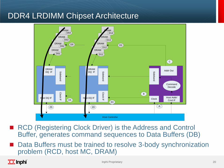
DDR4 LRDIMM Chipset Architecture
RCD (Registering Clock Driver) is the Address and Control Buffer, generates command sequences to Data Buffers (DB)
Data Buffers must be trained to resolve 3-body synchronization problem (RCD, host MC, DRAM)
Host DQ IF
Sid
eb
an
d
DRAM
DQ IFS
ide
ba
nd
Host Addr/
Cmd IF
Command
Decode
DRAM
Host Controller
Clock
Clo
ck IF
DRAM
DRAM
DRAM
Host DQ IF
Sid
eb
an
d
DRAM
DQ IF
DRAM
Clo
ck IF
DRAM
DRAM
DRAM
Addr Out
A
B
C
D1
E0E5
D5
Z0Z5
D11
D12
D13
D14
D52
D53
D54
D51
21 Inphi Proprietary
21 Inphi Proprietary
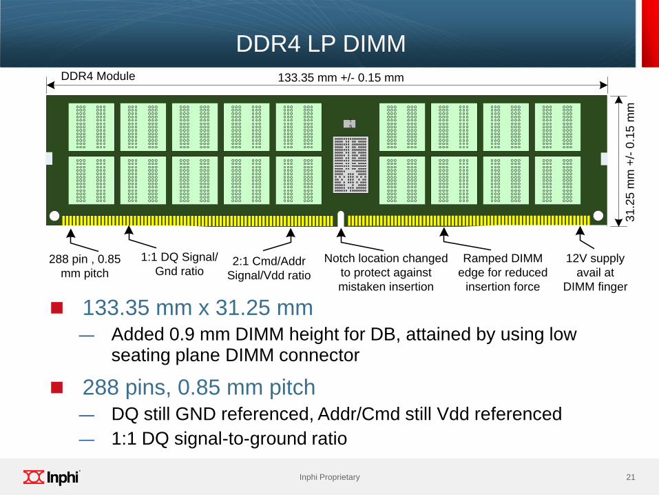
DDR4 LP DIMM
133.35 mm x 31.25 mm ― Added 0.9 mm DIMM height for DB, attained by using low
seating plane DIMM connector
288 pins, 0.85 mm pitch ― DQ still GND referenced, Addr/Cmd still Vdd referenced
― 1:1 DQ signal-to-ground ratio
133.35 mm +/- 0.15 mm
31
.25
mm
+/-
0.1
5 m
m
DDR4 Module
288 pin , 0.85
mm pitch
1:1 DQ Signal/
Gnd ratio2:1 Cmd/Addr
Signal/Vdd ratio
Ramped DIMM
edge for reduced
insertion force
Notch location changed
to protect against
mistaken insertion
12V supply
avail at
DIMM finger
T
S

22 Inphi Proprietary
22 Inphi Proprietary
DRAM Dimension for DDR4 LRDIMM
Ideally, DRAM Manufactures (SEC, Micron, Hynix) would like to place 36 Max Dimension DRAM Devices on Module ― 11.0 mm x 11.5 mm or 9 mm x 13 mm
DRAM devices cannot shrink (much) below 11.5 mm in y dimension due to ball footprint constraint
Data Buffer (DB) competes with DRAM for area ― DB needs to be as small as possible
9.6
mm
6.4 mm
a
c
e
b
d
f
gh
i
23 Inphi Proprietary
23 Inphi Proprietary
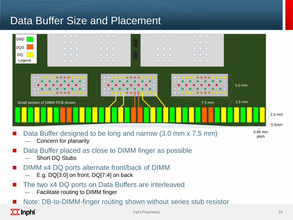
Data Buffer Size and Placement
Data Buffer designed to be long and narrow (3.0 mm x 7.5 mm) ― Concern for planarity
Data Buffer placed as close to DIMM finger as possible ― Short DQ Stubs
DIMM x4 DQ ports alternate front/back of DIMM ― E.g. DQ[3:0] on front, DQ[7:4] on back
The two x4 DQ ports on Data Buffers are interleaved ― Facilitate routing to DIMM finger
Note: DB-to-DIMM-finger routing shown without series stub resistor
0.5mm
2.0 mm
1.5 mm
0.85 mm
pitch
3.0 mm
Small section of DIMM PCB shown
GND
DQS
DQ
Legend
7.5 mm
24 Inphi Proprietary
24 Inphi Proprietary
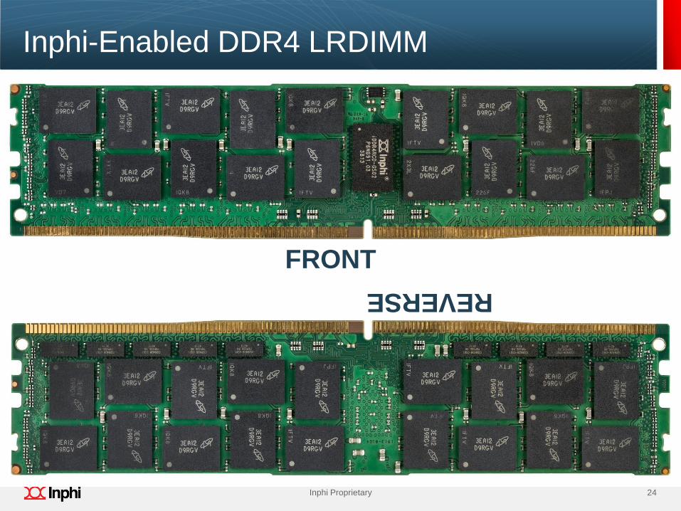
Inphi-Enabled DDR4 LRDIMM
FRONT
REVERSE

25 Inphi Proprietary
25 Inphi Proprietary
Ideal LRDIMM Component Placement
DRAM Devices in “vertical” orientation
Far easier to route Address, Command, Control and Clock Signals ― Relatively easier task of path length matching
133.35 mm
31
.25
mm

26 Inphi Proprietary
26 Inphi Proprietary
DDR4 LRDIMM R/C E Component Placement
“Windmill” or “Flower” supports DRAM devices with larger aspect ratios
27 Inphi Proprietary
27 Inphi Proprietary
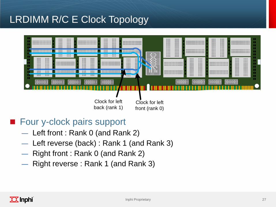
LRDIMM R/C E Clock Topology
Four y-clock pairs support ― Left front : Rank 0 (and Rank 2)
― Left reverse (back) : Rank 1 (and Rank 3)
― Right front : Rank 0 (and Rank 2)
― Right reverse : Rank 1 (and Rank 3)
Clock for left
front (rank 0)
Clock for left
back (rank 1)
28 Inphi Proprietary
28 Inphi Proprietary
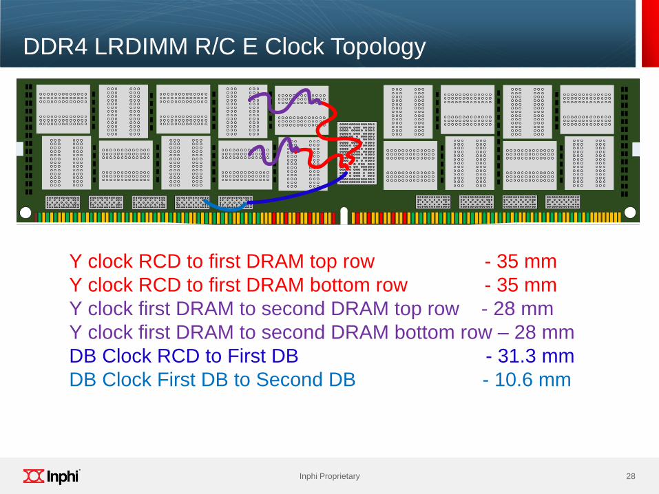
DDR4 LRDIMM R/C E Clock Topology
Y clock RCD to first DRAM top row - 35 mm
Y clock RCD to first DRAM bottom row - 35 mm
Y clock first DRAM to second DRAM top row - 28 mm
Y clock first DRAM to second DRAM bottom row – 28 mm
DB Clock RCD to First DB - 31.3 mm
DB Clock First DB to Second DB - 10.6 mm

29 Inphi Proprietary
29 Inphi Proprietary
DDR4 LRDIMM R/C E DRAM-to-DB DQ Routing
For each DB ― One nibble is on top row of a given slice
― Second nibble is on bottom of the same slice
Routing length differential between nibbles depends on slice (DB)
First DRAM top row to First DB – 32 mm
First DRAM bottom row to first DB - 27 mm
Last DRAM top row to First DB – 33 mm
Last DRAM bottom row to first DB - 11 mm
30 Inphi Proprietary
30 Inphi Proprietary
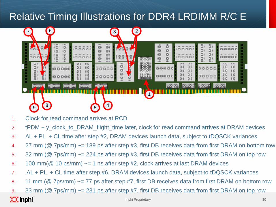
Relative Timing Illustrations for DDR4 LRDIMM R/C E
1
3
45
27 6
89
1. Clock for read command arrives at RCD
2. tPDM + y_clock_to_DRAM_flight_time later, clock for read command arrives at DRAM devices
3. AL + PL + CL time after step #2, DRAM devices launch data, subject to tDQSCK variances
4. 27 mm (@ 7ps/mm) ~= 189 ps after step #3, first DB receives data from first DRAM on bottom row
5. 32 mm (@ 7ps/mm) ~= 224 ps after step #3, first DB receives data from first DRAM on top row
6. 100 mm(@ 10 ps/mm) ~= 1 ns after step #2, clock arrives at last DRAM devices
7. AL + PL + CL time after step #6, DRAM devices launch data, subject to tDQSCK variances
8. 11 mm (@ 7ps/mm) ~= 77 ps after step #7, first DB receives data from first DRAM on bottom row
9. 33 mm (@ 7ps/mm) ~= 231 ps after step #7, first DB receives data from first DRAM on top row

31 Inphi Proprietary
31 Inphi Proprietary
Buffer on Board

32 Inphi Proprietary
32 Inphi Proprietary
Cisco UCS 4:1 Switched BoB on NHM Platform
Data buffers are 4:1 Switches
Address and Data Buffers on same side as CPU/DIMMs
Expands channel capacity from 2 DPC to 8 DPC
Total spacing is 42 DIMM positions across ― CPU occupies 12 DIMM positions
― Address and Data buffers occupy 2 DIMM positions per channel (total of 6)
― 6 + 12 + 24 = 42
19 inches (482.6 mm)
1.7
5 in
(4.4
4 m
m)
10.8 mm
(0.425 inch)
Channel A Channel B Channel C
Host Processor
33 Inphi Proprietary
33 Inphi Proprietary
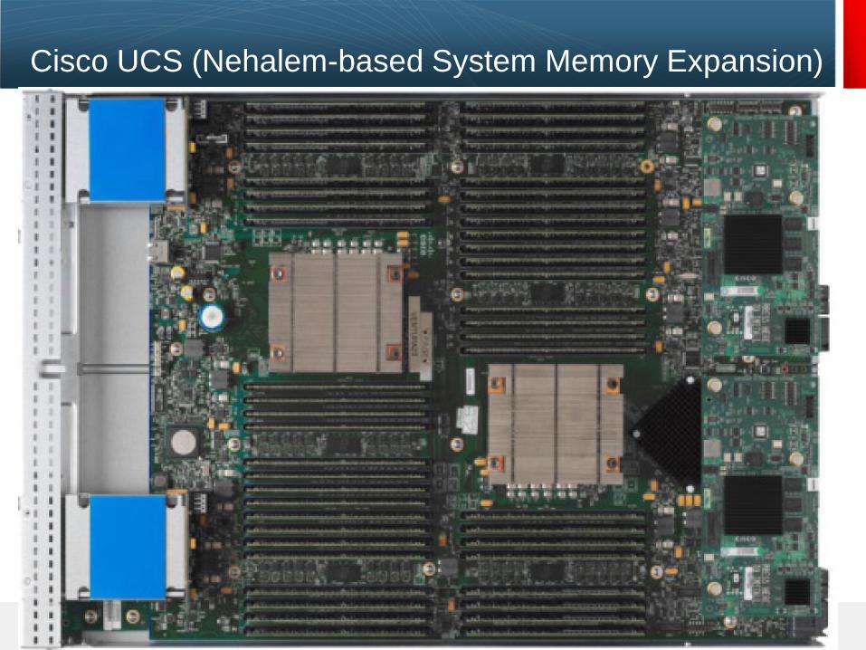
Cisco UCS (Nehalem-based System Memory Expansion)

34 Inphi Proprietary
34 Inphi Proprietary
IBM Power 7 High Speed Serdes to DDRx
35 Inphi Proprietary
35 Inphi Proprietary
Buffering Within Memory Stack
36 Inphi Proprietary
36 Inphi Proprietary
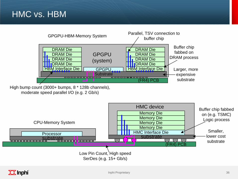
HMC vs. HBM
HBM Interface Die
Processorsubstrate
Memory Die
substrate
Memory DieMemory DieMemory Die
HMC Interface Die
DRAM DieDRAM DieDRAM DieDRAM Die
GPGPUSubstrate
GPGPU
(system)
HBM Interface DieDRAM DieDRAM DieDRAM DieDRAM Die
(FR4) PCB
(FR4) PCB
CPU-Memory System
GPGPU-HBM-Memory SystemParallel, TSV connection to
buffer chip
Larger, more
expensive
substrate
Buffer chip
fabbed on
DRAM process
HMC device
Smaller,
lower cost
substrate
Buffer chip fabbed
on (e.g. TSMC)
Logic process
Low Pin Count, High speed
SerDes (e.g. 15+ Gb/s)
High bump count (3000+ bumps, 8 * 128b channels),
moderate speed parallel I/O (e.g. 2 Gb/s)
37 Inphi Proprietary
37 Inphi Proprietary
Summary
38 Inphi Proprietary
38 Inphi Proprietary
Summary
Address and Data Buffers commonly used to improve pin-bandwidth/capacity of workstation and server platforms ― Multitudes of high-speed-serdes-to-DDRx solutions have been
implemented – AMB (FBDIMM), BoB
― Multitudes of DDRx-to-DDRx also implemented
Memory Buffers CAN do a lot more, but “doing more” typically means “higher cost”. ― Standard buffers are typically cost-optimized solutions
New Buffering concepts are being explored/implemented to do “interesting” things ― DRAM + NAND backup as NVDIMM for power-failure protection
― NAND-only Flash DIMM enables Flash devices to sit on DDR memory bus
― Use of new memory technology (MRAM, PCM, ReRAM) on DDRx memory bus