Embed Size (px)
Citation preview

NOTE: For detailed information on purchasing options, contact your local Allegro field applications engineer or sales representative.
Allegro MicroSystems, Inc. reserves the right to make, from time to time, revisions to the anticipated product life cycle plan for a product to accommodate changes in production capabilities, alternative product availabilities, or market demand. The information included herein is believed to be accurate and reliable. However, Allegro MicroSystems, Inc. assumes no respon-sibility for its use; nor for any infringements of patents or other rights of third parties which may result from its use.
Recommended Substitutions:For existing customer transition, and for new customers or new appli-cations, refer to the A1448.
Low-Voltage Full-Bridge Brushless DC Motor Driver with Hall Commutation, Externally Controlled Speed Regulation, Soft Switching,
and Reverse Battery, Short Circuit, and Thermal Shutdown Protection
A1444 and A1445
Date of status change: May 2, 2011
These parts are no longer in production The device should not be purchased for new design applications. Samples are no longer available.
Discontinued Product
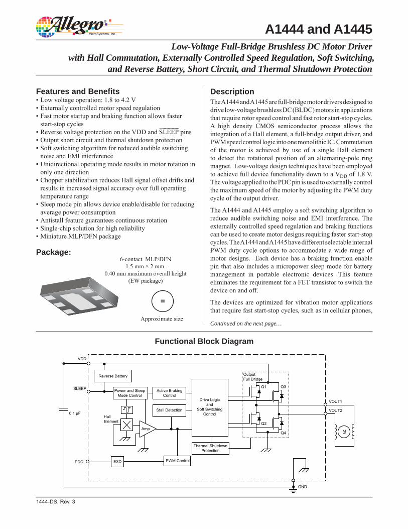
DescriptionThe A1444 and A1445 are full-bridge motor drivers designed to drive low-voltage brushless DC (BLDC) motors in applications that require rotor speed control and fast rotor start-stop cycles. A high density CMOS semiconductor process allows the integration of a Hall element, a full-bridge output driver, and PWM speed control logic into one monolithic IC. Commutation of the motor is achieved by use of a single Hall element to detect the rotational position of an alternating-pole ring magnet. Low-voltage design techniques have been employed to achieve full device functionality down to a VDD of 1.8 V. The voltage applied to the PDC pin is used to externally control the maximum speed of the motor by adjusting the PWM duty cycle of the output driver.
The A1444 and A1445 employ a soft switching algorithm to reduce audible switching noise and EMI interference. The externally controlled speed regulation and braking functions can be used to create motor designs requiring faster start-stop cycles. The A1444 and A1445 have different selectable internal PWM duty cycle options to accommodate a wide range of motor designs. Each device has a braking function enable pin that also includes a micropower sleep mode for battery management in portable electronic devices. This feature eliminates the requirement for a FET transistor to switch the device on and off.
The devices are optimized for vibration motor applications that require fast start-stop cycles, such as in cellular phones,
1444-DS, Rev. 3
Features and Benefits▪ Low voltage operation: 1.8 to 4.2 V▪ Externally controlled motor speed regulation▪ Fast motor startup and braking function allows faster
start-stop cycles▪ Reverse voltage protection on the VDD and S L E E P pins▪ Output short circuit and thermal shutdown protection▪ Soft switching algorithm for reduced audible switching
noise and EMI interference▪ Unidirectional operating mode results in motor rotation in
only one direction▪ Chopper stabilization reduces Hall signal offset drifts and
results in increased signal accuracy over full operating temperature range
▪ Sleep mode pin allows device enable/disable for reducing average power consumption
▪ Antistall feature guarantees continuous rotation▪ Single-chip solution for high reliability▪ Miniature MLP/DFN package
Low-Voltage Full-Bridge Brushless DC Motor Driver with Hall Commutation, Externally Controlled Speed Regulation, Soft Switching,
and Reverse Battery, Short Circuit, and Thermal Shutdown Protection
Continued on the next page…
Package:
Functional Block Diagram
A1444 and A1445
6-contact MLP/DFN1.5 mm × 2 mm.
0.40 mm maximum overall height(EW package)
Approximate size
Am
HallElement
p
Reverse Battery
Power and SleepMode Control
Active BrakingControl
Stall Detection
Drive Logicand
Soft SwitchingControl
GND
VDD
VOUT1
Output Full Bridge
Q1 Q3
Q2
Q4
SLEEP
VOUT2
Thermal ShutdownProtection
M
0.1 μF
PDC PWM ControlESD
Low-Voltage Full-Bridge Brushless DC Motor Driver with Hall Commutation, Externally Controlled Speed Regulation, Soft Switching,
and Reverse Battery, Short Circuit, and Thermal Shutdown Protection
A1444 and A1445
2Allegro MicroSystems, Inc.115 Northeast CutoffWorcester, Massachusetts 01615-0036 U.S.A.1.508.853.5000; www.allegromicro.com
Absolute Maximum RatingsCharacteristic Symbol Notes Rating Units
Forward Supply Voltage VDD 5.0 V
Reverse Supply Voltage VRDD –5.0 V
Forward Output Voltage VOUT VDD > 0 V 0 to VDD + 0.3 V
Reverse Output Voltage VROUT VDD > 0 V –0.3 V
S L E E P Input Voltage VIN 0 to VDD + 0.3 V
S L E E P Reverse Input Voltage VRIN –5.0 V
PDC Input Voltage VPDC –0.3 to VDD + 0.3 V
Continuous Output Current IOUTPositive ILOAD flow is from VOUT1 to VOUT2, TJ < TJ(max) ±250 mA
Peak Output Current IOUT(pk) <1 ms ±500 mA
Operating Ambient Temperature TA Range E –40 to 85 ºC
Maximum Junction Temperature TJ(max) 165 ºC
Storage Temperature Tstg –65 to 170 ºC
Description (continued)
Selection GuidePart Number Packing1 Package
A1444EEWLT-P23000 pieces per 7-in. reel 1.5 mm × 2 mm , 0.38 mm nominal overall package height,
6-contact MLP/DFN with exposed thermal padA1445EEWLT-P2
1Contact Allegro for additional packing options2Variant is in production but has been determined to be NOT FOR NEW DESIGN. This classification indicates that sale of the variant is currently restricted to existing customer applications. The variant should not be purchased for new design applications because obsolescence in the near future is probable. Samples are no longer available. Status change: May 4, 2009.
Thermal Characteristics may require derating at maximum conditions, see Power Derating sectionCharacteristic Symbol Test Conditions* Value Units
Package Thermal Resistance RθJA
On 2-layer PCB, with 0.23 in.2 copper area each side 125 ºC/W
On 4-layer PCB based on JEDEC standard 64 ºC/W
*Additional thermal information available on the Allegro website
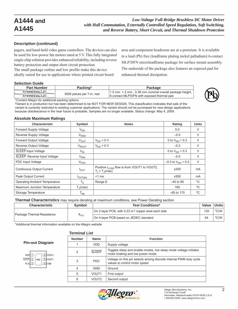
Pin-out Diagram
Terminal ListNumber Name Function
1 VDD Supply voltage
2 S L E E P Toggles sleep and enable modes, low sleep mode voltage initiates motor braking and low power mode
3 PDC Voltage on this pin selects among discrete internal PWM duty cycle values to control motor speed
4 GND Ground
5 VOUT1 First output
6 VOUT2 Second output
pagers, and hand-held video game controllers. The devices can also be used for low-power fan motors rated at 5 V. This fully integrated single-chip solution provides enhanced reliability, including reverse battery protection and output short circuit protection.The small package outline and low profile make this device ideally suited for use in applications where printed circuit board
area and component headroom are at a premium. It is available in a lead (Pb) free (leadframe plating nickel palladium) 6-contact MLP/DFN microleadframe package for surface mount assembly. The underside of the package also features an exposed pad for enhanced thermal dissipation.
VDD
SLEEP
PCD
VOUT2
VOUT1
GNDPAD
6
5
4
1
2
3
Low-Voltage Full-Bridge Brushless DC Motor Driver with Hall Commutation, Externally Controlled Speed Regulation, Soft Switching,
and Reverse Battery, Short Circuit, and Thermal Shutdown Protection
A1444 and A1445
3Allegro MicroSystems, Inc.115 Northeast CutoffWorcester, Massachusetts 01615-0036 U.S.A.1.508.853.5000; www.allegromicro.com
Continued on the next page...
ELECTRICAL CHARACTERISTICS Valid over supply voltage and ambient temperature ranges, unless otherwise notedCharacteristics Symbol Test Conditions Min. Typ.1 Max. Unit
Supply Voltage VDD TJ < TJ(max) 2.0 – 4.2 V
Extended Supply Voltage2 VDDE TJ < TJ(max) 1.8 – 4.2 V
Supply Current IDD(ON) VIN >VINHI , TA = 25°C, no load – 4 6 mA
VIN < V INLO , TA = 25°C – – 10 μA
Total Output On-Resistance3 RDS(on)
IOUT = 50 mA, VDD = 2 V, TA = 25°C – 3.9 – Ω
IOUT = 50 mA, VDD = 3 V, TA = 25°C – 2.6 – Ω
IOUT = 50 mA, VDD = 4 V, TA = 25°C – 2.2 – Ω
Reverse Battery Current IRDDVRDD = –4.2 V, current flowing out of VDD pin, TA = 25°C – – –10 mA
S L E E P Input Threshold VINHI 0.7 × VDD – – V
VINLO – – 0.2 × VDD V
S L E E P Input Current IIN VDD = 3.6 V – 1.0 5 μA
S L E E P Reverse Input Current IRIN VRIN = –4.2 V, current flowing out of S L E E P pin, TA = 25°C – – –10 mA
Restart Delay4 tRS VDD = 3.6 V – 100 – ms
Hall Chopping Settling Time5 tS(CHOP) – 160 – μs
Thermal Shutdown Limit TJTSD Device is active – 165 – °C
Thermal Shutdown Hysteresis TJTSD(HYS) Device is active – 20 – °C
Internal PWM Frequency fPWM – 40 – kHz
PDC High Level Threshold VPDCH PDC input going from low to high state VDD–0.5 – VDD V
PDC Low Level Threshold VPDCL PDC input going from high to low state 0 – 0.5 V
PDC Input Current6IPDCH Steady state condition, PDC pin high – – 30 μA
IPDCL Steady state condition, PDC pin low state –30 – – μA
Internal PWM Duty Cycle DCPWM
A1444
VPDC < VPDCL, VDD = VDDN, SROT > SROT(th)
– 56 – %
PDC Pin Floating, VDD = VDDN, SROT > SROT(th)
– 62 – %
VPDC > VPDCH, VDD = VDDN, SROT > SROT(th)
– 68 – %
A1445
VPDC < VPDCL, VDD = VDDN, SROT > SROT(th)
– 71 – %
PDC Pin Floating, VDD = VDDN,SROT > SROT(th)
– 80 – %
VPDC > VPDCH, VDD = VDDN, SROT > SROT(th)
– 89 – %

Low-Voltage Full-Bridge Brushless DC Motor Driver with Hall Commutation, Externally Controlled Speed Regulation, Soft Switching,
and Reverse Battery, Short Circuit, and Thermal Shutdown Protection
A1444 and A1445
4Allegro MicroSystems, Inc.115 Northeast CutoffWorcester, Massachusetts 01615-0036 U.S.A.1.508.853.5000; www.allegromicro.com
Magnetic Switchpoints
BOP 2 V ≤ VDD ≤ 4 V – 35 75 G
BRP 2 V ≤ VDD ≤ 4 V –75 –35 – G
BHYS 2 V ≤ VDD ≤ 4 V – 70 – G
Output Polarity
VOUT1B < BRP – LOW – V
B > BOP – HIGH – V
VOUT2B < BRP – HIGH – V
B > BOP – LOW – V1Typical data are for initial design estimations only, and assume optimum manufacturing and application conditions, such as TA = 25°C. Performance may vary for individual units, within the specified maximum and minimum limits.2Device operates with lower supply voltages, down to 1.8 V, with slight variation in specification of magnetic switchpoints and Total Output On-Resistance.3Total Output On-Resistance = RDS(on)Q1 + RDS(on)Q4 , or RDS(on)Q2 + RDS(on)Q3 , where Qx refers to the internal full-bridge transistors.4Restart Delay is the duration required from power-up of the device to valid device output.5Hall Chopping Settling Time is the delay from power-on of the device to the initial valid device output.6Positive current is defined as flowing into the device.
ELECTRICAL CHARACTERISTICS (continued) valid over supply voltage and ambient temperature ranges, unless otherwise notedCharacteristics Symbol Test Conditions Min. Typ. 1 Max. Unit
Low-Voltage Full-Bridge Brushless DC Motor Driver with Hall Commutation, Externally Controlled Speed Regulation, Soft Switching,
and Reverse Battery, Short Circuit, and Thermal Shutdown Protection
A1444 and A1445
5Allegro MicroSystems, Inc.115 Northeast CutoffWorcester, Massachusetts 01615-0036 U.S.A.1.508.853.5000; www.allegromicro.com
Functional Description
Soft Switching The A1444 and A1445 devices include a soft switching algorithm that controls the output switching slew rate for both output pins. As a result, the devices are ideal for use in applications requiring low audible switching noise and low EMI interference.
Braking and Sleep Mode The S L E E P pin accepts an external signal that enables braking and a sleep mode. During braking, the device reverses the polar-ity of the output bridge for a fixed time period, then the device enters sleep mode. In sleep mode, the device current consumption gets reduced to an extremely low level, conserving battery power.
Antistall Algorithm If a stall condition occurs, the device will execute an antistall algorithm to restart the motor.
Device Start-up
The start-up behavior of the device output is determined by the applied magnetic field, as specified in the Electrical Characteris-tics table.
Speed Control When the rate of rotation exceeds the specified threshold, SROT(th) , the A1444/A1445 output bridge becomes controlled by an internally generated PWM signal. The duty cycle of the inter-nal PWM signal regulates the maximum motor rpm. The PWM duty cycle, however, is user-selectable through the state of the PDC pin. The PWM duty cycle options are given in the Electrical Characteristics table.
Low-Voltage Full-Bridge Brushless DC Motor Driver with Hall Commutation, Externally Controlled Speed Regulation, Soft Switching,
and Reverse Battery, Short Circuit, and Thermal Shutdown Protection
A1444 and A1445
6Allegro MicroSystems, Inc.115 Northeast CutoffWorcester, Massachusetts 01615-0036 U.S.A.1.508.853.5000; www.allegromicro.com
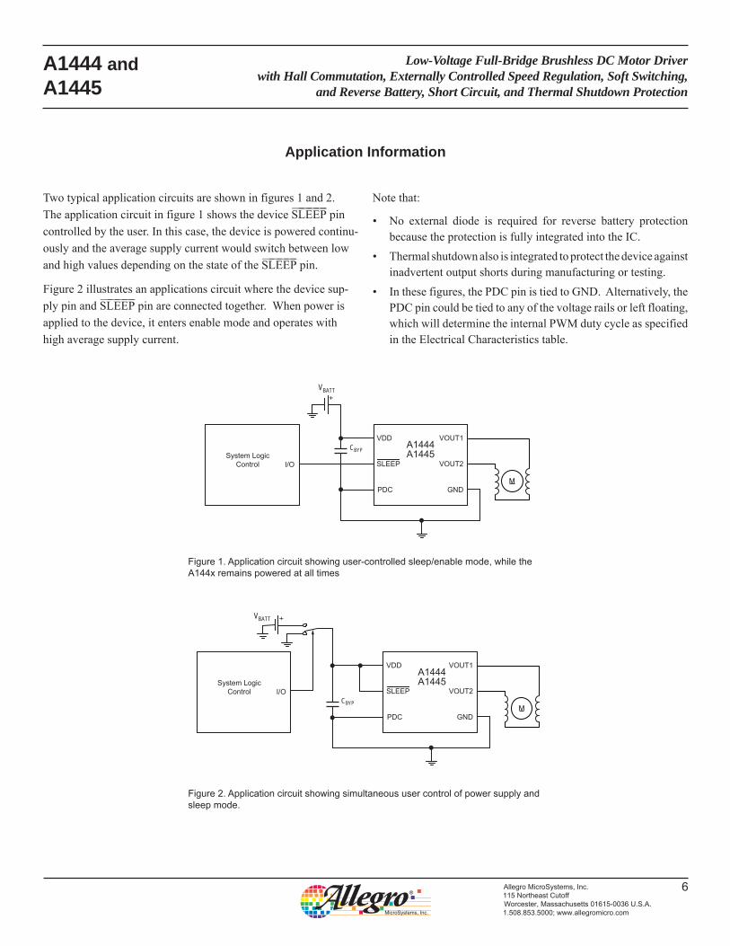
Two typical application circuits are shown in figures 1 and 2. The application circuit in figure 1 shows the device S L E E P pin controlled by the user. In this case, the device is powered continu-ously and the average supply current would switch between low and high values depending on the state of the S L E E P pin.
Figure 2 illustrates an applications circuit where the device sup-ply pin and S L E E P pin are connected together. When power is applied to the device, it enters enable mode and operates with high average supply current.
Note that:
• No external diode is required for reverse battery protection because the protection is fully integrated into the IC.
• Thermal shutdown also is integrated to protect the device against inadvertent output shorts during manufacturing or testing.
• In these figures, the PDC pin is tied to GND. Alternatively, the PDC pin could be tied to any of the voltage rails or left floating, which will determine the internal PWM duty cycle as specified in the Electrical Characteristics table.
Application Information
M
+VBATT
CBYPA1444A1445
PDC
VDD
I/OSystem Logic
Control
GND
VOUT1
SLEEP VOUT2
Figure 1. Application circuit showing user-controlled sleep/enable mode, while the A144x remains powered at all times
M
+VBATT
CBYP
A1444A1445
PDC
VDD
I/OSystem Logic
Control
GND
VOUT1
SLEEP VOUT2
Figure 2. Application circuit showing simultaneous user control of power supply and sleep mode.

Low-Voltage Full-Bridge Brushless DC Motor Driver with Hall Commutation, Externally Controlled Speed Regulation, Soft Switching,
and Reverse Battery, Short Circuit, and Thermal Shutdown Protection
A1444 and A1445
7Allegro MicroSystems, Inc.115 Northeast CutoffWorcester, Massachusetts 01615-0036 U.S.A.1.508.853.5000; www.allegromicro.com
Power Derating
The device must be operated below the maximum junction tem-perature of the device, TJ (max). Under certain combinations of peak conditions, reliable operation may require derating supplied power or improving the heat dissipation properties of the appli-cation. This section presents a procedure for correlating factors affecting operating TJ. (Thermal data is also available on the Allegro MicroSystems website.)
The package thermal resistance, RθJA, is a figure of merit sum-marizing the ability of the application and the device to dissipate heat from the junction (die), through all paths to the ambient air. Its primary component is the effective thermal conductivity, K, of the printed circuit board, including adjacent devices and traces. Radiation from the die through the device case, RθJC, is relatively small component of RθJA. Ambient air temperature, TA, and air motion are significant external factors, damped by overmolding.
The effect of varying power levels (Power Dissipation, PD), can be estimated. The following formulas represent the fundamental relationships used to estimate TJ, at various PD levels.
PD = VIN × IIN (1)
ΔT = PD × RθJA (2)
TJ = TA + ΔT (3)
For a load of 30 Ω, and given common conditions such as: TA= 25°C, VDD = 3 V, IDD = 85 mA, VLOAD = 2.43 V, ILOAD = 83 mA, and RθJA = 250 °C/W,
then:
PD = VDD × IDD – VLOAD × ILOAD
= 3 V × 83 mA – 2.43 V × 81 mA
= 52.17 mW
ΔT = PD × RθJA
= 52.17 mW × 250 °C/W
= 13°C
TJ = TA + ΔT
= 25°C + 13°C
= 38°C
A worst-case estimate, PD(max), represents the maximum allow-able power level, without exceeding TJ(max), at a selected RθJA and TA.

Low-Voltage Full-Bridge Brushless DC Motor Driver with Hall Commutation, Externally Controlled Speed Regulation, Soft Switching,
and Reverse Battery, Short Circuit, and Thermal Shutdown Protection
A1444 and A1445
8Allegro MicroSystems, Inc.115 Northeast CutoffWorcester, Massachusetts 01615-0036 U.S.A.1.508.853.5000; www.allegromicro.com
Copyright ©2009, Allegro MicroSystems, Inc.The products described herein are manufactured under one or more of the following U.S. patents: 5,045,920; 5,264,783; 5,442,283; 5,389,889;
5,581,179; 5,517,112; 5,619,137; 5,621,319; 5,650,719; 5,686,894; 5,694,038; 5,729,130; 5,917,320; and other patents pending.Allegro MicroSystems, Inc. reserves the right to make, from time to time, such de par tures from the detail spec i fi ca tions as may be required to per-
mit improvements in the per for mance, reliability, or manufacturability of its products. Before placing an order, the user is cautioned to verify that the information being relied upon is current.
Allegro’s products are not to be used in life support devices or systems, if a failure of an Allegro product can reasonably be expected to cause the failure of that life support device or system, or to affect the safety or effectiveness of that device or system.
The in for ma tion in clud ed herein is believed to be ac cu rate and reliable. How ev er, Allegro MicroSystems, Inc. assumes no re spon si bil i ty for its use; nor for any in fringe ment of patents or other rights of third parties which may result from its use.
For the latest version of this document, visit our website:www.allegromicro.com
Package EW, 6 pin MLP/DFN
SEATINGPLANE
0.38 ±0.02
0.70 ±0.10 1.25 ±0.05
0.25 ±0.05
1.10 ±0.10
1.10
0.30
0.70 1.575
0.50
0.325
2.00 ±0.15
1.50 ±0.15
C0.087X
0.325 +0.055–0.045
0.50 BSC
A
1
1
6
6
1
6
A Terminal #1 mark area
B Exposed thermal pad (reference only, terminal #1 identifier appearance at supplier discretion)
For Reference Only, not for tooling use (refernce DWG-2856; similar to JEDEC Type 1, MO-229X2BCD)Dimensions in millimetersExact case and lead configuration at supplier discretion within limits shown
C Reference land pattern layout (reference IPC7351 SON50P200X200X100-9M); All pads a minimum of 0.20 mm from all adjacent pads; adjust as necessary to meet application process requirements and PCB layout tolerances; when mounting on a multilayer PCB, thermal vias at the exposed thermal pad land can improve thermal dissipation (reference EIA/JEDEC Standard JESD51-5)
Active Area Depth 0.15 mm REFE
E
C
B
Hall Element (not to scale)F
F F
F0.94
0.99
PCB Layout Reference ViewC
Branding scale and appearance at supplier discretionG
G
D
D Coplanarity includes exposed thermal pad and terminals
Standard Branding Reference View
N = Last two digits of device part number Y = Last digit of year of manufacture W = Week of manufacture
NN YWW
1

DescriptionThe A1444 and A1445 are full-bridge motor drivers designed to drive low-voltage brushless DC (BLDC) motors in applications that require rotor speed control and fast rotor start-stop cycles. A high density CMOS semiconductor process allows the integration of a Hall element, a full-bridge output driver, and PWM speed control logic into one monolithic IC. Commutation of the motor is achieved by use of a single Hall element to detect the rotational position of an alternating-pole ring magnet. Low-voltage design techniques have been employed to achieve full device functionality down to a VDD of 1.8 V. The voltage applied to the PDC pin is used to externally control the maximum speed of the motor by adjusting the PWM duty cycle of the output driver.
The A1444 and A1445 employ a soft switching algorithm to reduce audible switching noise and EMI interference. The externally controlled speed regulation and braking functions can be used to create motor designs requiring faster start-stop cycles. The A1444 and A1445 have different selectable internal PWM duty cycle options to accommodate a wide range of motor designs. Each device has a braking function enable pin that also includes a micropower sleep mode for battery management in portable electronic devices. This feature eliminates the requirement for a FET transistor to switch the device on and off.
The devices are optimized for vibration motor applications that require fast start-stop cycles, such as in cellular phones,
1444-DS, Rev. 3
Features and Benefits▪ Low voltage operation: 1.8 to 4.2 V▪ Externally controlled motor speed regulation▪ Fast motor startup and braking function allows faster
start-stop cycles▪ Reverse voltage protection on the VDD and S L E E P pins▪ Output short circuit and thermal shutdown protection▪ Soft switching algorithm for reduced audible switching
noise and EMI interference▪ Unidirectional operating mode results in motor rotation in
only one direction▪ Chopper stabilization reduces Hall signal offset drifts and
results in increased signal accuracy over full operating temperature range
▪ Sleep mode pin allows device enable/disable for reducing average power consumption
▪ Antistall feature guarantees continuous rotation▪ Single-chip solution for high reliability▪ Miniature MLP/DFN package
Low-Voltage Full-Bridge Brushless DC Motor Driver with Hall Commutation, Externally Controlled Speed Regulation, Soft Switching,
and Reverse Battery, Short Circuit, and Thermal Shutdown Protection
Continued on the next page…
Package:
Functional Block Diagram
A1444 and A1445
6-contact MLP/DFN1.5 mm × 2 mm.
0.40 mm maximum overall height(EW package)
Approximate size
Am
HallElement
p
Reverse Battery
Power and SleepMode Control
Active BrakingControl
Stall Detection
Drive Logicand
Soft SwitchingControl
GND
VDD
VOUT1
Output Full Bridge
Q1 Q3
Q2
Q4
SLEEP
VOUT2
Thermal ShutdownProtection
M
0.1 μF
PDC PWM ControlESD

Low-Voltage Full-Bridge Brushless DC Motor Driver with Hall Commutation, Externally Controlled Speed Regulation, Soft Switching,
and Reverse Battery, Short Circuit, and Thermal Shutdown Protection
A1444 and A1445
2Allegro MicroSystems, Inc.115 Northeast CutoffWorcester, Massachusetts 01615-0036 U.S.A.1.508.853.5000; www.allegromicro.com
Absolute Maximum RatingsCharacteristic Symbol Notes Rating Units
Forward Supply Voltage VDD 5.0 V
Reverse Supply Voltage VRDD –5.0 V
Forward Output Voltage VOUT VDD > 0 V 0 to VDD + 0.3 V
Reverse Output Voltage VROUT VDD > 0 V –0.3 V
S L E E P Input Voltage VIN 0 to VDD + 0.3 V
S L E E P Reverse Input Voltage VRIN –5.0 V
PDC Input Voltage VPDC –0.3 to VDD + 0.3 V
Continuous Output Current IOUTPositive ILOAD flow is from VOUT1 to VOUT2, TJ < TJ(max) ±250 mA
Peak Output Current IOUT(pk) <1 ms ±500 mA
Operating Ambient Temperature TA Range E –40 to 85 ºC
Maximum Junction Temperature TJ(max) 165 ºC
Storage Temperature Tstg –65 to 170 ºC
Description (continued)
Selection GuidePart Number Packing1 Package
A1444EEWLT-P23000 pieces per 7-in. reel 1.5 mm × 2 mm , 0.38 mm nominal overall package height,
6-contact MLP/DFN with exposed thermal padA1445EEWLT-P2
1Contact Allegro for additional packing options2Variant is in production but has been determined to be NOT FOR NEW DESIGN. This classification indicates that sale of the variant is currently restricted to existing customer applications. The variant should not be purchased for new design applications because obsolescence in the near future is probable. Samples are no longer available. Status change: May 4, 2009.
Thermal Characteristics may require derating at maximum conditions, see Power Derating sectionCharacteristic Symbol Test Conditions* Value Units
Package Thermal Resistance RθJA
On 2-layer PCB, with 0.23 in.2 copper area each side 125 ºC/W
On 4-layer PCB based on JEDEC standard 64 ºC/W
*Additional thermal information available on the Allegro website
Pin-out Diagram
Terminal ListNumber Name Function
1 VDD Supply voltage
2 S L E E P Toggles sleep and enable modes, low sleep mode voltage initiates motor braking and low power mode
3 PDC Voltage on this pin selects among discrete internal PWM duty cycle values to control motor speed
4 GND Ground
5 VOUT1 First output
6 VOUT2 Second output
pagers, and hand-held video game controllers. The devices can also be used for low-power fan motors rated at 5 V. This fully integrated single-chip solution provides enhanced reliability, including reverse battery protection and output short circuit protection.The small package outline and low profile make this device ideally suited for use in applications where printed circuit board
area and component headroom are at a premium. It is available in a lead (Pb) free (leadframe plating nickel palladium) 6-contact MLP/DFN microleadframe package for surface mount assembly. The underside of the package also features an exposed pad for enhanced thermal dissipation.
VDD
SLEEP
PCD
VOUT2
VOUT1
GNDPAD
6
5
4
1
2
3

Low-Voltage Full-Bridge Brushless DC Motor Driver with Hall Commutation, Externally Controlled Speed Regulation, Soft Switching,
and Reverse Battery, Short Circuit, and Thermal Shutdown Protection
A1444 and A1445
3Allegro MicroSystems, Inc.115 Northeast CutoffWorcester, Massachusetts 01615-0036 U.S.A.1.508.853.5000; www.allegromicro.com
Continued on the next page...
ELECTRICAL CHARACTERISTICS Valid over supply voltage and ambient temperature ranges, unless otherwise notedCharacteristics Symbol Test Conditions Min. Typ.1 Max. Unit
Supply Voltage VDD TJ < TJ(max) 2.0 – 4.2 V
Extended Supply Voltage2 VDDE TJ < TJ(max) 1.8 – 4.2 V
Supply Current IDD(ON) VIN >VINHI , TA = 25°C, no load – 4 6 mA
VIN < V INLO , TA = 25°C – – 10 μA
Total Output On-Resistance3 RDS(on)
IOUT = 50 mA, VDD = 2 V, TA = 25°C – 3.9 – Ω
IOUT = 50 mA, VDD = 3 V, TA = 25°C – 2.6 – Ω
IOUT = 50 mA, VDD = 4 V, TA = 25°C – 2.2 – Ω
Reverse Battery Current IRDDVRDD = –4.2 V, current flowing out of VDD pin, TA = 25°C – – –10 mA
S L E E P Input Threshold VINHI 0.7 × VDD – – V
VINLO – – 0.2 × VDD V
S L E E P Input Current IIN VDD = 3.6 V – 1.0 5 μA
S L E E P Reverse Input Current IRIN VRIN = –4.2 V, current flowing out of S L E E P pin, TA = 25°C – – –10 mA
Restart Delay4 tRS VDD = 3.6 V – 100 – ms
Hall Chopping Settling Time5 tS(CHOP) – 160 – μs
Thermal Shutdown Limit TJTSD Device is active – 165 – °C
Thermal Shutdown Hysteresis TJTSD(HYS) Device is active – 20 – °C
Internal PWM Frequency fPWM – 40 – kHz
PDC High Level Threshold VPDCH PDC input going from low to high state VDD–0.5 – VDD V
PDC Low Level Threshold VPDCL PDC input going from high to low state 0 – 0.5 V
PDC Input Current6IPDCH Steady state condition, PDC pin high – – 30 μA
IPDCL Steady state condition, PDC pin low state –30 – – μA
Internal PWM Duty Cycle DCPWM
A1444
VPDC < VPDCL, VDD = VDDN, SROT > SROT(th)
– 56 – %
PDC Pin Floating, VDD = VDDN, SROT > SROT(th)
– 62 – %
VPDC > VPDCH, VDD = VDDN, SROT > SROT(th)
– 68 – %
A1445
VPDC < VPDCL, VDD = VDDN, SROT > SROT(th)
– 71 – %
PDC Pin Floating, VDD = VDDN,SROT > SROT(th)
– 80 – %
VPDC > VPDCH, VDD = VDDN, SROT > SROT(th)
– 89 – %
Low-Voltage Full-Bridge Brushless DC Motor Driver with Hall Commutation, Externally Controlled Speed Regulation, Soft Switching,
and Reverse Battery, Short Circuit, and Thermal Shutdown Protection
A1444 and A1445
4Allegro MicroSystems, Inc.115 Northeast CutoffWorcester, Massachusetts 01615-0036 U.S.A.1.508.853.5000; www.allegromicro.com
Magnetic Switchpoints
BOP 2 V ≤ VDD ≤ 4 V – 35 75 G
BRP 2 V ≤ VDD ≤ 4 V –75 –35 – G
BHYS 2 V ≤ VDD ≤ 4 V – 70 – G
Output Polarity
VOUT1B < BRP – LOW – V
B > BOP – HIGH – V
VOUT2B < BRP – HIGH – V
B > BOP – LOW – V1Typical data are for initial design estimations only, and assume optimum manufacturing and application conditions, such as TA = 25°C. Performance may vary for individual units, within the specified maximum and minimum limits.2Device operates with lower supply voltages, down to 1.8 V, with slight variation in specification of magnetic switchpoints and Total Output On-Resistance.3Total Output On-Resistance = RDS(on)Q1 + RDS(on)Q4 , or RDS(on)Q2 + RDS(on)Q3 , where Qx refers to the internal full-bridge transistors.4Restart Delay is the duration required from power-up of the device to valid device output.5Hall Chopping Settling Time is the delay from power-on of the device to the initial valid device output.6Positive current is defined as flowing into the device.
ELECTRICAL CHARACTERISTICS (continued) valid over supply voltage and ambient temperature ranges, unless otherwise notedCharacteristics Symbol Test Conditions Min. Typ. 1 Max. Unit

Low-Voltage Full-Bridge Brushless DC Motor Driver with Hall Commutation, Externally Controlled Speed Regulation, Soft Switching,
and Reverse Battery, Short Circuit, and Thermal Shutdown Protection
A1444 and A1445
5Allegro MicroSystems, Inc.115 Northeast CutoffWorcester, Massachusetts 01615-0036 U.S.A.1.508.853.5000; www.allegromicro.com
Functional Description
Soft Switching The A1444 and A1445 devices include a soft switching algorithm that controls the output switching slew rate for both output pins. As a result, the devices are ideal for use in applications requiring low audible switching noise and low EMI interference.
Braking and Sleep Mode The S L E E P pin accepts an external signal that enables braking and a sleep mode. During braking, the device reverses the polar-ity of the output bridge for a fixed time period, then the device enters sleep mode. In sleep mode, the device current consumption gets reduced to an extremely low level, conserving battery power.
Antistall Algorithm If a stall condition occurs, the device will execute an antistall algorithm to restart the motor.
Device Start-up
The start-up behavior of the device output is determined by the applied magnetic field, as specified in the Electrical Characteris-tics table.
Speed Control When the rate of rotation exceeds the specified threshold, SROT(th) , the A1444/A1445 output bridge becomes controlled by an internally generated PWM signal. The duty cycle of the inter-nal PWM signal regulates the maximum motor rpm. The PWM duty cycle, however, is user-selectable through the state of the PDC pin. The PWM duty cycle options are given in the Electrical Characteristics table.

Low-Voltage Full-Bridge Brushless DC Motor Driver with Hall Commutation, Externally Controlled Speed Regulation, Soft Switching,
and Reverse Battery, Short Circuit, and Thermal Shutdown Protection
A1444 and A1445
6Allegro MicroSystems, Inc.115 Northeast CutoffWorcester, Massachusetts 01615-0036 U.S.A.1.508.853.5000; www.allegromicro.com
Two typical application circuits are shown in figures 1 and 2. The application circuit in figure 1 shows the device S L E E P pin controlled by the user. In this case, the device is powered continu-ously and the average supply current would switch between low and high values depending on the state of the S L E E P pin.
Figure 2 illustrates an applications circuit where the device sup-ply pin and S L E E P pin are connected together. When power is applied to the device, it enters enable mode and operates with high average supply current.
Note that:
• No external diode is required for reverse battery protection because the protection is fully integrated into the IC.
• Thermal shutdown also is integrated to protect the device against inadvertent output shorts during manufacturing or testing.
• In these figures, the PDC pin is tied to GND. Alternatively, the PDC pin could be tied to any of the voltage rails or left floating, which will determine the internal PWM duty cycle as specified in the Electrical Characteristics table.
Application Information
M
+VBATT
CBYPA1444A1445
PDC
VDD
I/OSystem Logic
Control
GND
VOUT1
SLEEP VOUT2
Figure 1. Application circuit showing user-controlled sleep/enable mode, while the A144x remains powered at all times
M
+VBATT
CBYP
A1444A1445
PDC
VDD
I/OSystem Logic
Control
GND
VOUT1
SLEEP VOUT2
Figure 2. Application circuit showing simultaneous user control of power supply and sleep mode.
Low-Voltage Full-Bridge Brushless DC Motor Driver with Hall Commutation, Externally Controlled Speed Regulation, Soft Switching,
and Reverse Battery, Short Circuit, and Thermal Shutdown Protection
A1444 and A1445
7Allegro MicroSystems, Inc.115 Northeast CutoffWorcester, Massachusetts 01615-0036 U.S.A.1.508.853.5000; www.allegromicro.com
Power Derating
The device must be operated below the maximum junction tem-perature of the device, TJ (max). Under certain combinations of peak conditions, reliable operation may require derating supplied power or improving the heat dissipation properties of the appli-cation. This section presents a procedure for correlating factors affecting operating TJ. (Thermal data is also available on the Allegro MicroSystems website.)
The package thermal resistance, RθJA, is a figure of merit sum-marizing the ability of the application and the device to dissipate heat from the junction (die), through all paths to the ambient air. Its primary component is the effective thermal conductivity, K, of the printed circuit board, including adjacent devices and traces. Radiation from the die through the device case, RθJC, is relatively small component of RθJA. Ambient air temperature, TA, and air motion are significant external factors, damped by overmolding.
The effect of varying power levels (Power Dissipation, PD), can be estimated. The following formulas represent the fundamental relationships used to estimate TJ, at various PD levels.
PD = VIN × IIN (1)
ΔT = PD × RθJA (2)
TJ = TA + ΔT (3)
For a load of 30 Ω, and given common conditions such as: TA= 25°C, VDD = 3 V, IDD = 85 mA, VLOAD = 2.43 V, ILOAD = 83 mA, and RθJA = 250 °C/W,
then:
PD = VDD × IDD – VLOAD × ILOAD
= 3 V × 83 mA – 2.43 V × 81 mA
= 52.17 mW
ΔT = PD × RθJA
= 52.17 mW × 250 °C/W
= 13°C
TJ = TA + ΔT
= 25°C + 13°C
= 38°C
A worst-case estimate, PD(max), represents the maximum allow-able power level, without exceeding TJ(max), at a selected RθJA and TA.
Low-Voltage Full-Bridge Brushless DC Motor Driver with Hall Commutation, Externally Controlled Speed Regulation, Soft Switching,
and Reverse Battery, Short Circuit, and Thermal Shutdown Protection
A1444 and A1445
8Allegro MicroSystems, Inc.115 Northeast CutoffWorcester, Massachusetts 01615-0036 U.S.A.1.508.853.5000; www.allegromicro.com
Copyright ©2009, Allegro MicroSystems, Inc.The products described herein are manufactured under one or more of the following U.S. patents: 5,045,920; 5,264,783; 5,442,283; 5,389,889;
5,581,179; 5,517,112; 5,619,137; 5,621,319; 5,650,719; 5,686,894; 5,694,038; 5,729,130; 5,917,320; and other patents pending.Allegro MicroSystems, Inc. reserves the right to make, from time to time, such de par tures from the detail spec i fi ca tions as may be required to per-
mit improvements in the per for mance, reliability, or manufacturability of its products. Before placing an order, the user is cautioned to verify that the information being relied upon is current.
Allegro’s products are not to be used in life support devices or systems, if a failure of an Allegro product can reasonably be expected to cause the failure of that life support device or system, or to affect the safety or effectiveness of that device or system.
The in for ma tion in clud ed herein is believed to be ac cu rate and reliable. How ev er, Allegro MicroSystems, Inc. assumes no re spon si bil i ty for its use; nor for any in fringe ment of patents or other rights of third parties which may result from its use.
For the latest version of this document, visit our website:www.allegromicro.com
Package EW, 6 pin MLP/DFN
SEATINGPLANE
0.38 ±0.02
0.70 ±0.10 1.25 ±0.05
0.25 ±0.05
1.10 ±0.10
1.10
0.30
0.70 1.575
0.50
0.325
2.00 ±0.15
1.50 ±0.15
C0.087X
0.325 +0.055–0.045
0.50 BSC
A
1
1
6
6
1
6
A Terminal #1 mark area
B Exposed thermal pad (reference only, terminal #1 identifier appearance at supplier discretion)
For Reference Only, not for tooling use (refernce DWG-2856; similar to JEDEC Type 1, MO-229X2BCD)Dimensions in millimetersExact case and lead configuration at supplier discretion within limits shown
C Reference land pattern layout (reference IPC7351 SON50P200X200X100-9M); All pads a minimum of 0.20 mm from all adjacent pads; adjust as necessary to meet application process requirements and PCB layout tolerances; when mounting on a multilayer PCB, thermal vias at the exposed thermal pad land can improve thermal dissipation (reference EIA/JEDEC Standard JESD51-5)
Active Area Depth 0.15 mm REFE
E
C
B
Hall Element (not to scale)F
F F
F0.94
0.99
PCB Layout Reference ViewC
Branding scale and appearance at supplier discretionG
G
D
D Coplanarity includes exposed thermal pad and terminals
Standard Branding Reference View
N = Last two digits of device part number Y = Last digit of year of manufacture W = Week of manufacture
NN YWW
1