Embed Size (px)
Citation preview
Aalborg Universitet
Wear-out Failure Analysis of an Impedance-Source PV Microinverter Based on System-Level Electrothermal Modeling
Shen, Yanfeng; Chub, Andrii; Wang, Huai; Vinnikov, Dmitri; Liivik, Elizaveta; Blaabjerg,FredePublished in:I E E E Transactions on Industrial Electronics
DOI (link to publication from Publisher):10.1109/TIE.2018.2831643
Publication date:2019
Document VersionAccepted author manuscript, peer reviewed version
Link to publication from Aalborg University
Citation for published version (APA):Shen, Y., Chub, A., Wang, H., Vinnikov, D., Liivik, E., & Blaabjerg, F. (2019). Wear-out Failure Analysis of anImpedance-Source PV Microinverter Based on System-Level Electrothermal Modeling. I E E E Transactions onIndustrial Electronics, 66(5), 3914 - 3927. [8352545]. https://doi.org/10.1109/TIE.2018.2831643
General rightsCopyright and moral rights for the publications made accessible in the public portal are retained by the authors and/or other copyright ownersand it is a condition of accessing publications that users recognise and abide by the legal requirements associated with these rights.
- Users may download and print one copy of any publication from the public portal for the purpose of private study or research. - You may not further distribute the material or use it for any profit-making activity or commercial gain - You may freely distribute the URL identifying the publication in the public portal -
Take down policyIf you believe that this document breaches copyright please contact us at [email protected] providing details, and we will remove access tothe work immediately and investigate your claim.
0278-0046 (c) 2018 IEEE. Personal use is permitted, but republication/redistribution requires IEEE permission. See http://www.ieee.org/publications_standards/publications/rights/index.html for more information.
This article has been accepted for publication in a future issue of this journal, but has not been fully edited. Content may change prior to final publication. Citation information: DOI 10.1109/TIE.2018.2831643, IEEETransactions on Industrial Electronics
IEEE TRANSACTIONS ON INDUSTRIAL ELECTRONICS
Abstract—The wear-out performance of an impedance-source photovoltaic (PV) microinverter (MI) is evaluated and improved based on two different mission profiles. The operating principle and hardware implementation of the MI are firstly described. With the experimental measurements on a 300-W MI prototype and system-level finite element method (FEM) simulations, the electro-thermal models are built for the most reliability-critical components, i.e., power semi-conductor devices and capacitors. The dependence of the power loss on the junction/hotspot temperature is considered, the enclosure temperature is taken into account, and the thermal cross-coupling effect between components is modeled. Then the long-term junction/ hotspot temperature profiles are derived and further translated into components’ annual damages with the lifetime and damage accumulation models. After that, the Monte Carlo simulation and Weibull analysis are conducted to obtain the system wear-out failure probability over time. It reveals that both the mission profile and the thermal cross-coupling effect have a significant impact on the prediction of system wear-out failure, and the dc-link electrolytic capacitor is the bottleneck of long-term reliability. Finally, the multi-mode control with a variable dc-link voltage is proposed, and a more reliable dc-link electrolytic capacitor is employed, which results in a remarkable reliability improvement for the studied PV MI.
Index Terms—PV microinverter, reliability, wear out,
electro-thermal modeling
I. INTRODUCTION
VER the last decade, the solar photovoltaic (PV) energy
continues to experience a significant growth tendency due
to the dramatic price reduction of PV modules in the world
market [1], and the progressive evolution of PV converters
whose efficiency has been reported as high as 99% [2].
Compared to the central and string PV inverters, the
microinverters (MIs) feature more advantages in low power
applications such as module-level maximum power point
tracking (MPPT), low PV-system installation effort, and easy
condition monitoring and failure detection [3]-[5]. However,
there are also some challenges for PV MIs. First, the MIs are
normally cooled by natural convection and they are installed
close to the PV module, which means that they can be subjected
to a more extreme environment than central inverters typically
located in climate controlled environment [6]-[7]. In addition,
there is a trend that the MI will be incorporated into the module
frame in the future [6]. The lifetime/warranty of PV modules is
about 25 years, but the inverters have to be replaced every 5 to
10 years [8]; this implies that the lifetime of the MIs needs to
be extended to match that of the PV modules. Therefore,
reliability evaluation and reliability-oriented design of PV MIs
under a harsh environment is paramount [9]-[10].
Recently, increasing efforts have been made to the power
electronics reliability, especially to discrete components or
modules (e.g., IGBT, MOSFET, and capacitor) [10]-[20]. Only
a few works [10], [13], [19] focus on the system-level reliability
but not for PV module-level power electronics (MLPE). In
addition, one significant drawback of previous general
reliability assessments is that the local ambient temperature and
the thermal cross-coupling effect between components are not
considered; thus, the reliability performance might be
overestimated. Based on a failure mode and effects analysis
(FMEA) survey for MLPE products [21], the loose connection
of dc input and ac output connectors, wear-out of dc-link
electrolytic capacitors, varistor failure-short from the surge, and
degradation of MOSFETs and diodes are identified as the top
four failure modes; meanwhile, temperature cycling is reported
as the most important stressor that affects the reliability of
MLPE products. Only a few studies focused on the MI
reliability can be found in literature, and most of them use the
MIL-HDBK-217 handbook [22] to determine the failure rates
of MIs [20]. Unfortunately, the constant failure rates only
describe the large-population statistics of random failures, and
the wear-out failure is not considered. Meanwhile, the MLPE
Wear-out Failure Analysis of an Impedance-Source PV Microinverter Based on System-Level Electro-Thermal Modeling
Yanfeng Shen, Student Member, IEEE, Andrii Chub, Member, IEEE, Huai Wang, Senior Member, IEEE, Dmitri Vinnikov, Senior Member, IEEE,
Elizaveta Liivik, Member, IEEE, and Frede Blaabjerg, Fellow, IEEE.
O
Manuscript received Dec. 10, 2017; revised Mar. 22, 2018; accepted Apr. 17, 2018. This work was supported in part by the Innovation Fund Denmark through the Advanced Power Electronic Technology and Tools (APETT) project, in part by the Estonian Centre of Excellence in Zero Energy and Resource Efficient Smart Buildings and Districts under Grant 2014-2020.4.01.15-0016, in part by the European Regional Development Fund, and in part by the Estonian Research Council under project PUT1443. (Corresponding author: Yanfeng Shen) Yanfeng Shen, Huai Wang, Elizaveta Liivik, and Frede Blaabjerg are with the Department of Energy Technology, Aalborg University, 9220 Aalborg, Denmark (e-mail: [email protected], [email protected], [email protected], [email protected]). Andrii Chub is with the Department of Electrical Power Engineering and Mechatronics, Tallinn University of Technology, 19086 Tallinn, Estonia (e-mail: [email protected]). Dmitri Vinnikov is with the Department of Electrical Power Engineering and Mechatronics, Tallinn University of Technology, 19086 Tallinn, Estonia, and is also with Ubik Solutions LLC, 11911 Tallinn, Estonia (e-mail: [email protected]). Color versions of one or more of the figures in this paper are available online at http://ieeexplore.ieee.org.

0278-0046 (c) 2018 IEEE. Personal use is permitted, but republication/redistribution requires IEEE permission. See http://www.ieee.org/publications_standards/publications/rights/index.html for more information.
This article has been accepted for publication in a future issue of this journal, but has not been fully edited. Content may change prior to final publication. Citation information: DOI 10.1109/TIE.2018.2831643, IEEETransactions on Industrial Electronics
IEEE TRANSACTIONS ON INDUSTRIAL ELECTRONICS
TX
1:n
* *
VPV
Lm
Llk=Lr
SqZS
CqZS1
V1
S1
S2
S3
S4
VTX,prCdc
* *LlkqZS
LmqZS
1:1
LqZS
LlkqZSC1=Cr
C2=Cr
CqZS2
PV
module
Grid-tied inverter and output filter Synchronous quasi-Z-source series resonant DC-DC converter
Cf
Lf1
S5
S6
S7
S8
Grid
Vg
Ig
D1
D2
Integrated series
resonant tankLf2
IТХ,pr
Vdc
Fig. 1. Schematic of the impedance-source PV microinverter.
Fig. 2. Photo of the built PV microinverter prototype.
market is relatively nascent and there is not enough long-term
usage data or independent reliability testing; therefore,
accelerated testing of PV MI products is conducted in [6] for a
long-term reliability prediction. It turns out that the time-to-
failure of MIs from different manufacturers deviates
significantly due to the design.
The PV MI system demands a wide input voltage and load
regulation range at high DC voltage gains [23]. The impedance-
source converters featuring the immunity to shoot-through and
open states, continuous input current, low inrush current, buck-
boost functionality as well as high control flexibility, and thus
have recently gained much attention [24]-[25]. In [26], a quasi-
Z-source series resonant dc-dc converter (qZSSRC) is proposed
for MLPE applications; with a multimode control, the qZSSRC
is capable of maintaining high efficiency within the six-fold
variation of the input voltage (10~60 V). This feature enables the
implementation of the shade-tolerant (global) MPPT, thus
ensuring the maximum possible energy yield from the PV
module even when two out of three substrings are shaded or in
the conditions of opaque shading which could be caused by the
fallen leaves or bird droppings [27]. Alternatively to the shoot-
through pulse width modulation (PWM) and phase-shift
modulation (PSM) in [26], the qZSSRC could also be controlled
by the asymmetrical PWM [28], variable frequency [29] or the
topology morphing [30], which significantly widens gain range
and increases application flexibility.
Although the impedance-source converters properly match
the demanding requirements of the PV MLPE application, their
reliability performance is an open question. This paper aims to
investigate the wear-out failure of an impedance-source PV MI.
A mission profile based system-level wear-out assessment
method is proposed and applied. A detailed electro-thermal
model is built with the aid of system-level finite element method
(FEM) simulations and experimental measurements on a 300-W
MI prototype. Then, the mission profiles are translated into long-
term junction/hotspot temperature profiles and annual damages
for components. The Monte Carlo simulation and Weibull
analysis are conducted to obtain the system wear-out failure over
time. Finally, the variable dc-link voltage control is applied and
the electrolytic capacitor is replaced with a more reliable one to
improve system reliability. Compared with conventional
reliability assessments, several improvements are made: 1) the
dependence of component power loss on the junction/hotspot
temperature is experimentally characterized and applied; 2)
system-level FEM simulations are performed and the enclosure
temperature is incorporated into the electro-thermal model; 3)
the thermal cross-coupling effect between components is
considered and modeled.
II. SYSTEM DESCRIPTION AND RELIABILITY EVALUATION
A. System Description
The schematic of the impedance-source PV MI is shown in
Fig. 1. The two-stage MI consists of the quasi-Z-source series
resonant dc-dc converter (qZSSRC) and the full-bridge inverter.
The detailed operation principle and parameter design guidelines
have been presented in [26]. There are three operation modes for
the front-end qZSSRC:
1) Pass-Through Mode (PTM): The qZSSRC operates as the
series-resonant converter (SRC) in the DC transformer mode.
The normalized DC voltage gain is unity [26]:
12dc
PTMPV
VG
nV (1)
2) Buck Mode: The operation of the qZSSRC is similar to that
of the SRC with phase-shift modulation (PSM) control at the
resonant frequency and discontinuous resonant current. The
latter is due to small leakage inductance values of conventional
transformers (Q≪1). The normalized DC voltage gain depends
on the phase shift angle φ and the quality factor Q as in [26]:
2 2( )
80.5
2dc
buck DCMPV
VG AB A B A
nV Q (2)
where (1 cos[ (1 /180)]) / 2A , 2 /( ) 1B Q ,
and 2(8 ) /sw lk dc dcQ f L P V .
3) Boost Mode: the voltage is controlled by shoot-through pulse
width modulation (ST-PWM) implemented as a symmetrical
overlap of active states. The normalized DC voltage gain in this
mode depends on the shoot-through duty cycle DST [26]:
1
2 1 2DC
boostPV ST
VG
nV D. (3)
A 300-W PV MI prototype, consisting of the main circuit,
auxiliary power supply circuit and microcontroller unit (MCU),
has been built, as shown in Fig. 2. The detailed specifications
and parameters are given in Table I. The measured full-load
waveforms and efficiency curves at different input voltages and
power levels are shown in Fig. 3.

0278-0046 (c) 2018 IEEE. Personal use is permitted, but republication/redistribution requires IEEE permission. See http://www.ieee.org/publications_standards/publications/rights/index.html for more information.
This article has been accepted for publication in a future issue of this journal, but has not been fully edited. Content may change prior to final publication. Citation information: DOI 10.1109/TIE.2018.2831643, IEEETransactions on Industrial Electronics
IEEE TRANSACTIONS ON INDUSTRIAL ELECTRONICS
80
82
84
86
88
90
92
94
96
50 100 150 200 250 300
Eff
icie
ncy
(%
)
Output power (W)
Vpv = 20 V
Vpv = 30 V
Vpv = 40 V
V1 (20 V/div)
0
ITX,pr (5 A/div)
VTX,pr (20 V/div)
0
Time: 1 ms/div
V1 (10 V/div)
Time: 1 ms/div
0
ITX,pr (5 A/div)
VTX,pr (10 V/div)
(a) (b)
(c) (d)
(e) (f)
89
90
91
92
93
94
95
96
20 25 30 35 40
Eff
icic
ien
cy (
%)
Input voltage VPV (V)
250 W 200 W150 W 100 W50 W
Ig (0.5 A/div)
Vg (100 V/div)
0
0
V1 (10 V/div)
ITX,pr (5 A/div)
VTX,pr (10 V/div)
Time: 10 ms/div
Time: 1 ms/div
0
Fig. 3. Experimental waveforms in the (a) pass-through mode, (b) buck mode, and (c) boost mode. (d) Measured grid voltage and current waveforms. Measured efficiency curves of (e) the dc-dc stage and (f) the whole microconverter including the auxiliary power supply.
TABLE I
SPECIFICATIONS AND PARAMETERS OF THE MICROINVERTER PROTOTYPE Descriptions Parameters
Input voltage range 1060 V
Nominal voltage 33 V
Most probable operating voltage range 2040 V Rated power 300 W
Switch. frequency of dc-dc stage 110 kHz
Switch. frequency of inverter stage 20 kHz
Switches SqZS, S1…S4 BSC035N10NS5
Switches S5…S8 SCT2120AFC
Diodes D1…D2 C3D02060E
Capacitors CqZS1 and CqZS2 2.2 mF 12, C1210C225K1R
Coupled inductor LqZS LmqZS=12 µH, LlkqZS=0.6 µH, custom
Resonant capacitors C1 and C2 10 nF // 33 nF, MKP1840310104M
and B32672Z6333K
DC-link capacitor Cdc 150 µF, 500-V electrolytic capacitor
Grid-side LCL filter: capacitor Cf 470 nF, B32653A6474K
Inductors Lf1 2.6 mH, custom
Inductors Lf2 1.8 mH, custom Transformer TX Lm=1 mH, Llk=24 µH, n=6, custom
B. Reliability Evaluation Process
The failure modes of a power electronics system include the
hardware failure, software failure and human error [10], as
shown in Fig. 4. The hardware failure consists of the
catastrophic, random, burn-in and wear-out failures. According
to the FMEA survey for MLPE products in [21], connector
contact failure, wear-out of electrolytic capacitor, short-circuit
of varistor, and degradation of MOSFET/diode are reported as
the top-four frequently happened failure modes, and the
temperature cycling is identified as the most critical stressor
affecting reliability. Therefore, this paper evaluates the wear-out
failure of critical components, i.e., power semiconductors and
capacitors, based on the flowchart illustrated in Fig. 4.
Fig. 4. Failure modes of power electronics systems and evaluation flowchart of the hardware wear-out failure probability.
The real-field mission profile, i.e., the solar irradiance (SI)
and ambient temperature Ta for the PV MI system, directly
determines the electrical and thermal loadings, and thus affects
the degradation process of the components. With a PV panel
model and an MPPT control, the long-term mission profile can
be translated into the real-time voltage and power at the
maximum power point, VPV(mpp) and PPV(mpp), which are the input
of the MI. The power loss and junction/hotspot temperature of a
component can be subsequently calculated based on the
electrical and thermal models. The rainflow counting algorithm
[31] is employed to extract the number of temperature cycles
with different characteristics (e.g., the mean junction
temperature Tjm, and the temperature swing Tj). After that, the
lifetime and damage accumulation models can be used to
estimate the accumulated damage over a year. The
junction/hotspot temperature Tj also affects the power loss,
which is taken into account. When the damage is accumulated to
1, it is assumed that the component fails. Then the static wear-
out lifetime of a component can be derived. In the real world,
however, the parameters of the component and lifetime models
have variations, which would affect the distribution of wear-out
PV panel
model and
MPPT
control
Electrical
model
Thermal
model
SI
Ta
Vmpp
Pmpp
PlossTj
Rainflow
counting
algorithm
Lifetime and
damage
modelsTj, Tjm
Monte Carlo
simulation
Weibull
distribution
fit
Tj
Ta
Dmg
Parameter
variations
Component
parameters:
Rds,on, ESR,
Rth, etc.
Lifetime
parameters:
a, m, etc.
System
reliability
model
...
Lif
eti
me
n s
ampl
es
Time
pd
f
1
( )t
tf t e
System wear-out
failure probability
Catastrophic
failure
Software
failure
Human
error
Random
failure
Burn-in
failure
...F1(t) F2(t) Fn(t)
Series reliability model
Ftot(t) = 1 (1Fi(t) )
Hardware failure
System reliability
Mission profile

0278-0046 (c) 2018 IEEE. Personal use is permitted, but republication/redistribution requires IEEE permission. See http://www.ieee.org/publications_standards/publications/rights/index.html for more information.
This article has been accepted for publication in a future issue of this journal, but has not been fully edited. Content may change prior to final publication. Citation information: DOI 10.1109/TIE.2018.2831643, IEEETransactions on Industrial Electronics
IEEE TRANSACTIONS ON INDUSTRIAL ELECTRONICS
(a) (b)
(c) (d)
Fig. 5. Measured current characteristics of critical components. (a) RMS and (b) off-switching currents of primary-side components in the dc-dc stage; (c) RMS currents of secondary-side devices in the dc-dc stage; (d) RMS currents of inverter-stage devices.
Fig. 6. Temperature characteristics of MOSFETs and an electrolytic capacitor. (a) Dependence of the on-state resistance Rds,on on the junction temperature for MOSFETs. (b) Dependence of ESR (at 100 Hz) on the hotspot temperature for the aluminum electrolytic capacitor used in the prototype.
failure probability. Therefore, a sensitivity analysis—Monte
Carlo simulation is conducted based on a large population of
samples. With the Weibull distribution fitting, the probability
density function (pdf) for each component can be derived; and
the system wear-out failure probability finally can be obtained
with the reliability model for a series connected system.
III. ELECTRO-THERMAL AND LIFETIME MODELING OF
CRITICAL COMPONENTS
A. Power Loss Modeling
1) Power Semiconductor Devices
The current stress characteristics are measured for critical
components, as shown in Fig. 5. The power loss of MOSFETs
consists of the conduction loss PT,con, turn-on loss PT,on, and turn-
off loss PT,off. The conduction loss calculation is straight-forward,
i.e., 2
, , ,T con T rms ds onP I R , where IT,rms is the root-mean-square
(RMS) current flowing through the MOSFET and Rds,on
represents its on-state resistance which is a function of the
junction temperature (cf. Fig. 6(a)). For the MOSFETs (SqZS, S1-
S4) in the dc-dc converter stage, their soft-switching conditions
depend on the operation modes, as illustrated in [26]. For the
inverter stage, the unipolar modulation is applied and the
MOSFETs are hard-switched. The switching losses of
MOSFETs are calculated with the model given in [32]. Two SiC
Schottky diodes C3D02060E are employed for D1-D2, and the
conduction loss is derived by 2
, , 0 , ,D con D avg D D rms D onP I V I R , where
VD0 = 0.98 0.0011 × TjD, RD,on = 0.18 + 0.0018 × TjD [33], and
TjD is the junction temperature of the diode.
2) Capacitors
For the MI, the instantaneous power p(t) contains a fluctuating
power at twice the line frequency, which is decoupled by the dc-
link capacitor Cdc. The electrical stresses over Cdc can be
calculated by [34]
0 ,/ ( ), / ( 2 )dc dc dc Cdc rms dcV P C V I P V (4)
where P is the average power injected to the grid, ΔVdc is the
peak-to-peak ripple of the capacitor voltage Vdc, and ICdc,rms is the
RMS current flowing through Cdc. The aluminum electrolytic
dc-link capacitor Cdc can be modeled as an ideal capacitor in
series with an equivalent series resistor (ESR) [34]-[35]. There
are two degradation mechanisms for the electrolytic capacitors
[9]: chemical reactions due to electrolyte evaporation and
contaminants, leading to deterioration of the dielectric material;
localized heating, ion transport, and chemical processes caused
by the leakage current [36]. The main stressor is the internal
hotspot temperature Th that is determined by the power loss 2
, , ( )Cdc loss Cdc rms hP I ESRT . The ESR of an electrolytic capacitor
is temperature dependent [37]-[38]; the temperature
characteristic of the used electrolytic capacitor is measured and
modeled as shown in Fig. 6(b).
For the ceramic and film capacitors (Cqzs, Cr1-Cr2 and Cf), their
power losses can be calculated in a similar way. However, their
temperature characteristics are different from electrolytic
capacitors. For the polypropylene film capacitors, the
dependency of their capacitance on the temperature is very weak
(0.023%/oC); in the meanwhile, the dissipation factor (DF) is
largely unaffected by temperature [39]-[40]. Similarly, when the
hotspot temperature is increased from 0 oC to 100 oC, the
capacitance and DF of X7R ceramic capacitors decrease by only
5% and 1.5%, respectively [41]. Therefore, the impact of hotspot
temperature on the power losses of polypropylene film and X7R
ceramic capacitors are neglected in this paper.
3) Magnetic Components
The power losses of magnetic components consist of the core
loss and the winding loss. The improved generalized Steinmetz
equation (iGSE) [42] describes core loss, and the winding loss
can be obtained with the Dowell model [43]-[44]. All the
magnetic components were implemented with the Ferrite core
3C95 whose power loss density curve is flat with respect to
temperature; this holds for various conditions of frequency and
flux density [45]. Hence, the temperature dependence of the
power losses in magnetic components is neglected.
B. Thermal Modeling
The PV MI is built with a four-layer PCB and is enclosed in
an aluminum case (200 mm150mm45mm) by natural cooling.
The case is filled up with elastic 2-component polyurethane
casting compound [46] whose thermal conductivity (0.7
W/(Km)) is almost 30 times higher than that of still air. Thus,
the thermal cross-coupling effect between components (heat
sources) cannot be neglected. However, most manufacturers
provide the junction/core-ambient or case-ambient thermal
resistance of a single component in a specific cooling condition.
(a) (b)

0278-0046 (c) 2018 IEEE. Personal use is permitted, but republication/redistribution requires IEEE permission. See http://www.ieee.org/publications_standards/publications/rights/index.html for more information.
This article has been accepted for publication in a future issue of this journal, but has not been fully edited. Content may change prior to final publication. Citation information: DOI 10.1109/TIE.2018.2831643, IEEETransactions on Industrial Electronics
IEEE TRANSACTIONS ON INDUSTRIAL ELECTRONICS
Fig. 7. Structure models of the main components, enclosure and PCB (including traces and vias) built in ANSYS/Icepak for FEM simulations. The PCB and the enclosure are placed horizontally. The enclosure is naturally cooled, i.e., all faces are exposed to the open air.
Black: Pl = 1 W
Red: Pl = 5 W
Blue: Pl = 10 W
Magenta: Pl = 15 W
Green: Pl = 20 W
Markers: FEM
Lines: Fit
(a) (b) Fig. 8. (a) FEM simulated and (b) fitted enclosure-to-ambient thermal impedance at different power loss levels and enclosure locations.
Fig. 9. Thermal impedance network of an enclosed converter system, including the self and mutual junction-enclosure thermal impedances.
Zoom in
Resin inside enclosure 68.49
56.37
44.24
32.12
20.00Zoom in
26.06
38.18
50.31
62.43
Fig. 10. FEM thermal simulation results in the case of total power loss Pl,tot = 17.5 W. Temperature contour plane cut in the front view.
Apparently, these values cannot be used in the thermal
analysis. Also, the mutual thermal resistance (thermal cross-
coupling) depends on the heat transfer medium and the
geometry/layout of components. Therefore, system-level FEM
simulations are conducted to extract the self and mutual thermal
resistances.
1) Enclosure-to-Ambient Thermal Impedance
The heat conduction, convection and radiation all exist in the
thermal transfer from the enclosure to the circumstance. The heat
transfer rate of convection is related to the temperature gap
between the surface and the circumstance, whereas radiation
intensity depends on the absolute temperature [47]-[48].
The enclosure of the studied MI is a custom hollow elliptical
cylinder (cf. Fig. 7), which makes it difficult to analytically
obtain the enclosure-to-ambient thermal impedance Zthea.
Therefore, multiple FEM simulations with ANSYS/Icepak are
conducted at different power loss values and enclosure points, as
shown in Fig. 8(a). It can be seen that the enclosure location has
a negligible impact on Zthea, i.e., it is almost isothermal, as the
Aluminum and the filled compound have a high thermal
conductivities. The enclosure-to-ambient thermal impedance
Zthea is a function of the total power loss of the MI, Pl, as well as
time, and can be fitted as a first-order Foster model (cf. Fig.8(b))
/( )(1 e )thea theat R Cthea theaZ R (5)
where Cthea is found to be constant as 2673 J/oC but Rthea is a
function of the total power loss, 0.2163.5thea lR P . It should
be noted that the enclosure is placed horizontally in all the FEM
simulations above. If the microinverter is installed vertically in
practice, then the FEM-simulated thermal resistance is found as 0.2133.45thea lR P which is very close to that in the
horizontal orientation. Hence, for this custom aluminum
enclosure, it can be assumed that the enclosure-to-ambient
thermal impedance Zthea is independent of its orientation.
2) Junction-to-Enclosure Thermal Impedance Network
Thermal resistance network of a converter with N main
components (heat sources) is shown in Fig. 9. The mutual
thermal impedance is present between the components. It is
difficult to perform the analytical calculation because of the
irregular geometry of heat transfer medium. Conduction is the
main heat transfer way inside the compound-filled converter,
i.e., the components and compound inside the enclosure form a
linear and time-invariant (LTI) system [49]. Therefore, the
superposition principle can be applied [50]-[51] and the junction
temperature for each component can be obtained by
1 11 12 1 1
2 21 22 2 2
1 2
( ) ( ) ( ) ( ) ( )
( ) ( ) ( ) ( ) ( )d
d
( ) ( ) ( ) ( ) ( )
j je je je N l
j je je je N le
jN jeN jeN jeNN lN
T t Z t Z t Z t P t
T t Z t Z t Z t P tT
t
T t Z t Z t Z t P t
(6)
where Tji is the junction/hotspot temperature of component i,
Zjenn represents the self junction/hotspot-to-enclosure thermal
impedance, Zjemn denotes the mutual junction/hotspot-to-
enclosure thermal impedance between components m and n, Te
is the enclosure temperature, Pln is the power loss of the nth
component, and "*" denotes convolution.
Detailed structure models for all main components, enclosure,
and PCB (including traces and vias) are built in ANSYS/Icepak
based on real dimensions and material properties, as shown in
Fig.7. To extract the thermal impedances in (6), multiple system-
level FEM simulations are conducted, as shown in Fig. 10. It can
be seen that the local ambient temperature of each component
has no significant difference due to the filled compound. The self
thermal impedance of S1 and mutual thermal impedances
between S1 and other components are depicted in Fig. 11(a). The
Enclosure (Al)
Magnetic components
MOSFETs
Film capacitors
MOSFETs
Diodes
Electrolytic
capacitor
4-layer PCB
Light blue lines:
traces, vias, and pads Circumstance
Simulation
boundary
*
Loc. 2
(top)
Loc. 3
(top)
Loc. 1
(top)
Loc. 4
(top)
Loc. 5
(bottom)
Pl1
Pl2
Pl3
PlN
Ta
Zth12 Zth23 Zth34
Zth1n
Zth2n
Zth13
Zth
je1
Zth
je2
Zth
je3
Zth
jeN
Tj1
Zth3n
Tj2 Tj3 TjN
Te
Zthea
Ambient temperature
Enclosure temperature
0278-0046 (c) 2018 IEEE. Personal use is permitted, but republication/redistribution requires IEEE permission. See http://www.ieee.org/publications_standards/publications/rights/index.html for more information.
This article has been accepted for publication in a future issue of this journal, but has not been fully edited. Content may change prior to final publication. Citation information: DOI 10.1109/TIE.2018.2831643, IEEETransactions on Industrial Electronics
IEEE TRANSACTIONS ON INDUSTRIAL ELECTRONICS
ZjeCr1&ZjeCr2
ZjeCqzs
ZjeCf
ZjeCdc
ZjeLqzs,ZjeTx
&ZjeLf
ZjeS5ZjeS8
ZjeD1&ZjeD2
ZjeSqzs,
ZjeS1ZjeS4
Self thermal
impedance ZjeS1
ZjcS1Mutual thermal
impedance ZjemS1
(a)
(b)
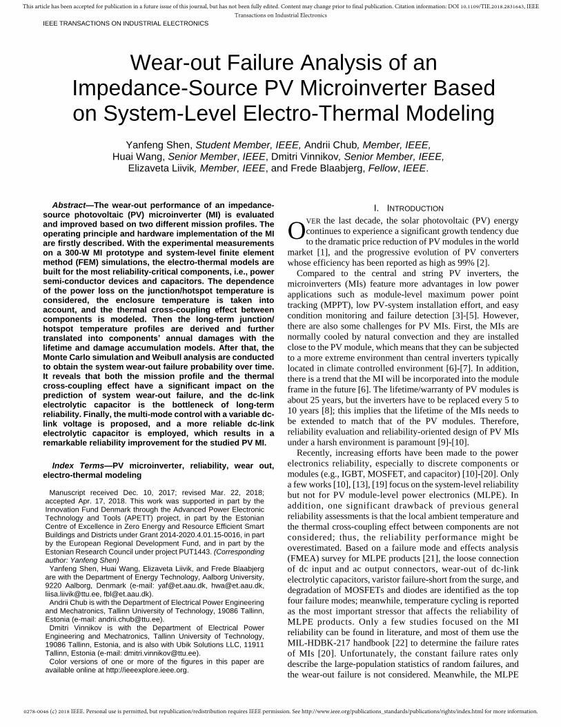
(c) Fig. 11. FEM simulation results for thermal impedances. (a) Junction-case and junction-enclosure thermal impedances of S1; mutual junction-enclosure thermal impedances between S1 and other components. Self junction-enclosure thermal impedances of (b) semiconductor devices and (c) passive components.
self thermal impedance of semiconductor devices and passive
components are shown in Fig. 11(b) and (c).
There are 19 main heat sources in the given MI. To speed up
the subsequent calculation for the long-term junction
temperature, the adjacent devices with the same part number and
the same power loss are combined into one heat source. Thus,
S1-S2, S3-S4, S5-S6, S7-S8, D1-D2 and Cr1-Cr2 are simplified into
S12, S34, S56, S78, D12 and Cr12, respectively. With the system-level
FEM simulations, the junction-enclosure thermal resistance (i.e.,
steady-state thermal impedance) matrix also can be obtained:
8.5 0.95 0.3 0 0 0 0.73 0 0 0 1.1 0 0
0.96 5 0.5 0 0 0 1 0 0 0 1 0.35 0
0.29 0.5 4.9 0 0 0 0.34 0.54 0 0 0.31 1 0
0 0 0 3.4 1.1 0.25 0 0 0.8 0.85 0 0 0.36
0 0 0 1.1 3.4 0.16 0 0 0.58 0.7 0 0 0.22
0 0 0 0.23 0.16 5.2 0 0.34 0.33 0 0 0.2 0.3
0.72 1 0.36 0 0 0 15.5 0 0 0 0.76 0.3 0
0 0 0.51 0
jeR
0 0.32 0 20.4 0 0 0 0.7 0
0 0 0 0.8 0.56 0.32 0 0 5.8 0.73 0 0 0.4
0 0 0 0.84 0.7 0 0 0 0.74 20.6 0 0 0.42
1.1 1 0.33 0 0 0 0.74 0 0 0 2 0.29 0
0 0.3 1 0 0 0.16 0.23 0.7 0 0 0.27 1.95 0
0 0 0 0.35 0.21 0.34 0 0 0.4 0.42 0 0 2
(7)
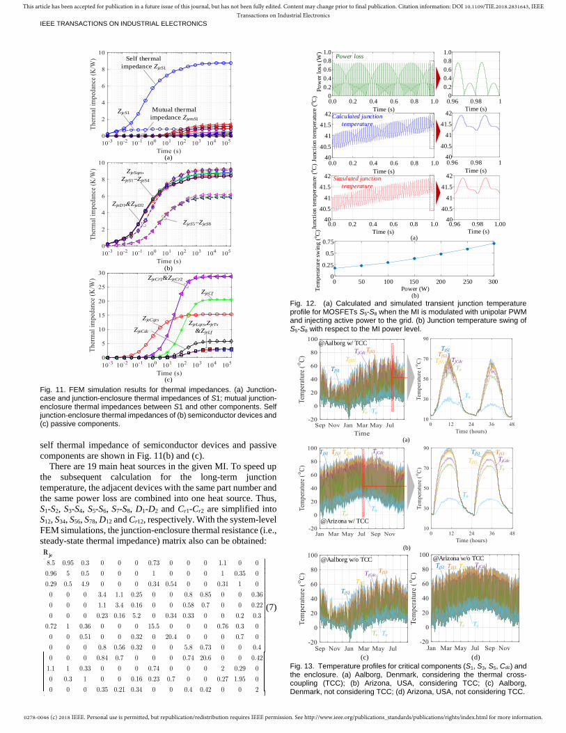
Fig. 12. (a) Calculated and simulated transient junction temperature profile for MOSFETs S5-S8 when the MI is modulated with unipolar PWM and injecting active power to the grid. (b) Junction temperature swing of S5-S8 with respect to the MI power level.
TjS1
TjS3
TjS5
TjCdc
Te Ta
(a)
TjS1 TjS3 TjS5 TjCdc
Te
Ta
(b)
(c) (d)
@Aalborg w/ TCC
@Arizona w/ TCC
@Arizona w/o TCC@Aalborg w/o TCCTjS1 TjS3 TjS5 TjCdc
Te Ta
TjS1
TjS3
TjS5
TjCdc
Te Ta
TjS1
TjS3TjCdcTjS5
Ta
Te
TjS1 TjS3
TjCdc
Te
Ta
TjS5
Fig. 13. Temperature profiles for critical components (S1, S3, S5, Cdc) and the enclosure. (a) Aalborg, Denmark, considering the thermal cross-coupling (TCC); (b) Arizona, USA, considering TCC; (c) Aalborg, Denmark, not considering TCC; (d) Arizona, USA, not considering TCC.
Time (s)
Tem
per
ature
(oC
)
Time (s)
Power loss
Calculated junction
temperature
Simulated junction
temperature
(a)
1.0
0.8
0.6
0.4
0.2
00.96 0.98 1
42
41.5
41
40.5
400.96 0.98 1
42
41.5
41
40.5
400.96 0.98 1.00.80.60.40.2
42
41.5
41
40.5
42
41.5
41
40.5
40
Juncti
on
tem
per
atu
re (
oC
)Ju
ncti
on
tem
per
atu
re (
oC
)
1.0
0.8
0.6
0.4
0.2
0
Po
wer
loss
(W)
1.00.80.60.40.20.0
1.00.80.60.40.20.0
Time (s)
Time (s)
Time (s) Time (s)
Time (s)
Time (s)
Power (W)(b)
0.0
0 50 100 150 200 250 300
Tem
pera
ture
sw
ing (
oC
)
0.75
0.5
0.25
0
1.0040

0278-0046 (c) 2018 IEEE. Personal use is permitted, but republication/redistribution requires IEEE permission. See http://www.ieee.org/publications_standards/publications/rights/index.html for more information.
This article has been accepted for publication in a future issue of this journal, but has not been fully edited. Content may change prior to final publication. Citation information: DOI 10.1109/TIE.2018.2831643, IEEETransactions on Industrial Electronics
IEEE TRANSACTIONS ON INDUSTRIAL ELECTRONICS
where the diagonal elements are the self thermal resistances and
the non-diagonal elements represent the mutual thermal
resistances. Analyzing the degree of symmetry of (7) yields
|| ( ) / 2 ||
0.39%|| ( ) / 2 ||
mS'
je je
'je je
R R
R R. (8)
This implies that the thermal resistance matrix has a fairly
high degree of symmetry due to the reciprocity of heat
conduction [50]-[51]. The thermal impedance Zjemn can be fitted
as a Kth-order Foster model:
,/,
1
(1 )jemn k
Kt
jemn jemn kk
Z R e (9)
where Rjemn and jemn are junction-enclosure thermal resistance
and time constant between components m and n. The ambient-
enclosure temperature difference and the junction temperature
of component m can be calculated from the discrete equations:
,
,
/,
/1 1 , ,
/ /,
( )( 1)
( ) (1 )
( 1) ( ) ( ) (1 )
( 1) ( 1) ( 1)
mn k
mn k
ea ea
tN Kjemn k
jem tn k l n mn k
t tea ea l tot ea
jm jem ea a
T x eT x
P x R e
T x T x e P x R e
T x T x T x T
(10)
The unipolar pulse width modulation (PWM) [52] is applied
to the inverter stage, and it is assumed that only active power is
injected to the grid. During the positive half cycle of the grid
voltage, S5 and the body diode of S6 turn on alternately, and S8
and the body diode of S7 conduct alternately. During the negative
half cycle, S6 and the body diode of S5 turn on alternately, and S7
and the body diode of S8 conduct alternately. The channel of
each MOSFET conducts during a half cycle, whereas the body
diode conducts during the other half cycle. The (conduction and
switching) power losses of the MOSFET channel and its body
diode are different, leading to an asymmetrical power loss
profile for the MOSFETs in the inverter stages, as shown in
Fig. 12(a). Fig. 12 also presents the calculated and simulated
junction temperature profiles of S5-S8 for 300-W active power
injected to the grid. Evidently, their junction temperature profile
has 50-Hz fluctuations, which are caused by the periodical
power losses at 50 Hz. The calculations agree well with
simulations. The amplitude of the 50-Hz temperature swing rises
with respect to the MI power increase, as indicated in Fig. 12(b).
C. Lifetime and Damage Accumulation Modeling
According to the FMEA results in [12] and [18], the
progressive increase of the on-state resistance (wear-out) of
MOSFETs is mainly caused by the growth of fatigue cracks and
voids into the source metal layer. A 20% rise of the on-state
resistance is chosen as the criteria of wear-out failure and a
Coffin-Manson law based reliability model is built in [12]
( ) mf jN T (11)
where Nf is the number of cycles to failure, Tj is the junction
temperature swing, and a and m are fitting parameters.
A widely-used capacitor lifetime model is employed for the
lifespan projection of capacitors [15], [19]
0
1 20 02 ( / )
hT T
n ncn cL L V V (12)
in which Lcn is the lifetime under the thermal and electrical stress
Th and V, Lc0 is the lifetime under the reference temperature T0
and the nominal voltage V0. The coefficient n1 is a temperature
dependent constant, and n2 is the voltage stress exponent.
For snap-in aluminum electrolytic capacitors, the
temperature-dependent parameter n1 is 10 and the voltage stress
exponent n2 is 5 when the applied voltage is 80 %-100 % of the
rated voltage [53]-[54]. The temperature-dependent parameter
n1 = 10 also holds for film capacitors [15], [36], [57]. However,
the voltage stress exponent n2 for film capacitors is reported
from around 7 to 9.4 in [9], [15], [36], from 5 to 10 in [55], from
7 to 12 in [56], and 7 in [57]. The discrepancy between the values
may be attributed to the different technologies adopted by the
different manufacturers [55]. To have an unbiased lifetime
estimation of film capacitors, the median value 8.2 is adopted.
For the ceramic capacitor used, the manufacturer provides the
coefficients n1 = 8, and n2 = 3 [58].
According to the commonly used Miner’s rule [59]-[60], the
damage accumulates linearly:
( / )mg k fkk
D n N (13)
where nk is the number of cycles with a specific thermal loading
stress, and Nfk is the number of cycles till failure for the same
stress. The device fails when the accumulated Dmg reaches 1.
IV. WEAR-OUT FAILURE ANALYSIS OF THE MICROINVERTER
A. Static Annual Damage of Components
The mission profiles from Aalborg, Denmark, and Arizona,
USA, are applied to the electro-thermal model. Then, the
junction/hotspot temperature profiles for each component and
the enclosure temperature can be derived (cf. Fig. 13). The
resolution is 100 points/s to accommodate 50-Hz junction
temperature fluctuations of the inverter MOSFETs. If the
thermal cross-coupling (TCC) effect is not considered, the
junction/hotspot temperatures of components will be
underestimated, as shown in Fig. 13(c) and (d). It should be
noted that a MI is typically installed on the mounting rack of PV
panels, and thus the real ambient temperature of the MI may be
higher than the applied one which represents the open-field
temperature. The PV module degradation is ignored to offset this
methodology flaw.
With and without considering the TCC effect, the annual
damage of each critical component at the two locations is shown
in Fig. 14(a). It can be observed that the dc-link capacitor Cdc has
the highest annual damage at both locations, i.e., 0.01 and 0.057
for Aalborg and Arizona, respectively. Assuming there are no
other kinds of failures, the corresponding wear-out lifetimes of
the dc-link capacitor are 100 yrs and 17.54 yrs for the two
operating locations. However, if the thermal cross-coupling
effect is not considered, then the annual damages of Cdc at the
two locations are 0.007 and 0.031, which results in an
underestimation rate of about 30 %. The mean ambient
temperature of Arizona over a year, Tam, is 22.34 °C. If the solar
irradiance of Arizona remains the same, but the mean ambient
temperature Ta varies, then the annual damage of each
component will change as well, as shown in Fig. 14(b). It can be
seen that the annual damages of capacitors rise significantly with
respect to the increase of Tam, while the damages of
semiconductors increase slightly. This results from (11) where
the number of cycles to failure is mainly dependent on the
junction temperature swing instead of its mean value.

0278-0046 (c) 2018 IEEE. Personal use is permitted, but republication/redistribution requires IEEE permission. See http://www.ieee.org/publications_standards/publications/rights/index.html for more information.
This article has been accepted for publication in a future issue of this journal, but has not been fully edited. Content may change prior to final publication. Citation information: DOI 10.1109/TIE.2018.2831643, IEEETransactions on Industrial Electronics
IEEE TRANSACTIONS ON INDUSTRIAL ELECTRONICS
(a)
(b)
Arizona, w/ TCC
Annual mean ambient
temperature of Arizona
Fig. 14. Annual damage to each critical component. (a) Annual damage when the MI operates at different locations with and without considering the thermal cross-coupling (TCC). (b) Annual damage of each component versus the mean ambient temperature in Arizona.
95 % CI95 % CI
Cdc@Aalborg
w/ TCC
Cdc@Aalborg
w/o TCC Cdc@Arizona
w/o TCC
Cdc@Arizona
w/ TCC
(a)
(b)
Bar: simulated
Line: fitted
Cdc@Aalborg
w/ TCC
Cdc@Aalborg
w/o TCC
Cdc@Arizona
w/o TCC
Cdc@Arizona
w/ TCC
Fig. 15. (a) Probability density functions of the parameters for the dc-link capacitor Cdc; (b) Histograms of years to wear-out failure for a population of 1×10⁵ capacitor samples operating at two locations, with and without considering the TCC effect.
B. Monte Carlo Simulation and System Failure Probability Due to Wear-out
There are some uncertainties which may affect the MI lifetime
in the real-world operation. First, the parameters in the lifetime
model could vary. For instance, the applied lifetime model for
MOSFETs is derived from the testing data in [12], and the
parameters a and m have boundaries. Second, the parameters of
the employed devices vary, which is caused by the
manufacturing process variations among the devices with the
same part number. According the datasheet, the on-state
resistances of the MOSFETs employed in the two stages vary
within ±20% and ±10%, respectively. Third, the mission profile
could also vary due to the climate change.
95 % CI95 % CI95 % CI
S1@Aalborg w/ TCCS1@Aalborg w/o TCC
S1@Arizona
w/o TCCS1@Arizona
w/ TCC
S1@Aalborg
w/ TCCS1@Aalborg
w/o TCC
S1@Arizona
w/o TCCS1@Arizona
w/ TCC
Bar: simulated
Line: fitted
(a)
(b)
m
Fig. 16. (a) Probability density functions of the parameters for S1; (b) Histograms of years to wear-out failure for a population of 1×10⁵ samples operating at two locations, with and without considering the TCC effect.
@Aalborg,
w/ TCC
Cdc
CapacitorsSemiconductors
CapacitorsSemiconductors
Cdc
S1
@Aalborg,
w/o TCC
SystemSystem
S1
System
Cdc
System
Cdc
@Arizona,
w/ TCC@Arizona,
w/o TCC
B10
8.3
yrs
B10
12.2
yrs
S1 S1
(a) (b)
(c) (d)
Fig. 17. Probability curves of wear-out failure for each component and the system when operating at (a) Aalborg, Denmark, with considering the thermal cross-coupling (TCC) effect; (b) Aalborg, Denmark, without considering the TCC effect o; (c) Arizona, US, with considering the TCC effect; (d) Arizona, US, without considering the TCC effect.
It is assumed that all the variations mentioned above obey the
normal distribution. The second and third types of uncertainties
(e.g., Rds,on of MOSFET, ESR of capacitor, ambient
temperature, and solar irradiance) directly affect the
junction/hotspot temperature. Hence, the junction/hotspot
temperature swing will vary within a certain range. The
probability density functions (pdfs) of the parameters of Cdc and
S1 are shown in Figs. 15(a) and 16(a), considering a 95%
confidence interval (CI). For other devices, their parameters
variations are also considered.
To analyze the impact of all the uncertainties on the system
wear-out failure, the continuous mission profile should be
converted into an equivalent static one, which produces the same
degradation [61]. Then a sensitivity analysis—Monte Carlo
simulation can be carried out by simultaneously taking into
account all parameter variations. The population number for
each sample is 1×10⁵ in the Monte Carlo simulation. The
histograms of years to wear-out failure for the selected

0278-0046 (c) 2018 IEEE. Personal use is permitted, but republication/redistribution requires IEEE permission. See http://www.ieee.org/publications_standards/publications/rights/index.html for more information.
This article has been accepted for publication in a future issue of this journal, but has not been fully edited. Content may change prior to final publication. Citation information: DOI 10.1109/TIE.2018.2831643, IEEETransactions on Industrial Electronics
IEEE TRANSACTIONS ON INDUSTRIAL ELECTRONICS
ST-PWM controlled
boost mode
Pass-through
mode
(range)
PSM controlled
buck mode
18
21
24
27
30
33
36
39
42
45
- 1. 00 - 0. 88 - 0. 75 - 0. 63 - 0. 50 - 0. 38 - 0. 25 - 0. 13 0.00 0.13 0.25 0.38 0.50
Inp
ut v
olt
age (
V)
50 W
100 W
200 W
180 0 0.2545135 90
variation of DSTvariation of
VDC = 460 V
VDC = 335 V
60-cell
MPPs
72-cell
MPPs
NOCT
NOCT
0.5
VPV(min)
ST-PWM
VPV
VDC(min)
VDC(max)
No control PSM
VDC
Boost mode
Pass-through mode
Buck mode
Mode
Control
VPV1 VPV2
0VPV(max)
(a) (b) Fig. 18. Advanced multi-mode control of the qZSSRC with a variable dc-link voltage: (a) sketch of dc-link voltage variations; (b) regulation characteristics.
82
84
86
88
90
92
94
96
0 50 100 150 200 250 300
Eff
icie
ncy
(%
)
Input power (W)
25 V 28 V
33 V 38 V93
94
95
96
97
98
99
0 50 100 150 200 250 300
Eff
icie
ncy
( %
)
Output power (W)
25 V 28 V
33 V 38 V
(a) (b) Fig. 19. Measured efficiency with the new control strategy: (a) the whole PV MI incl. the auxiliary power, (b) the dc-dc power stage.
components, Cdc and S5, are shown in Figs. 15(b) and 16(b),
respectively, which are fitted with the Weibull distribution [61]:
1
( ) , ( ) 1t t
tf t e F t e (14)
where β is the shape parameters and is the scale parameter.
Assume all the considered devices are connected in series in
the reliability model, i.e., any component failure will lead to
system failure. Then the system wear-out failure Fsys(t) equals:
( ) 1 (1 ( ))sys iF t F t (15)
where Fi(t) represents the cumulative distribution function (cdf)
of the component wear-out failure.
Fig. 17 shows the probability curves of wear-out failures for
components and the system when operating at Aalborg,
Denmark, and Arizona, US, with and without considering the
thermal cross-coupling effect. First, it can be seen that the
mission profile has a strong impact on the wear-out failure: when
operating in a harsher environment, i.e., Arizona, the wear-out
failure probabilities before 25-year operation are significantly
higher. Second, neglecting the thermal cross-coupling effect will
lead to an obvious underestimation of the wear-out failure
probability; when operating at Aalborg, the predicted system
wear-out failure probability before 25 years is 3.34 % (cf. Fig.
17(a)), whereas the corresponding value is only 1.3 % (cf. Fig.
17(b)) if neglecting the thermal cross-coupling effect. When
operating at Arizona, the B10 lifetimes with and without
considering the thermal cross-coupling effect are 8.3 yrs and
12.2 yrs (cf. Fig. 17(c) and (d)), respectively, which implies that
about 45 % lifetime overestimation can be made if neglecting
the thermal cross-coupling effect. In addition, it can be seen that
the dc-link electrolytic capacitor Cdc has the highest wear-out
failure probability when the operating environment is harsh, and
thus dominates the system wear-out failure. Hence, it can be
concluded that the dc-link electrolytic capacitor Cdc is the
bottleneck of 25-year reliable operation for the studied PV MI.
V. RELIABILITY IMPROVEMENT OF THE MICROINVERTER
It can be concluded from the reliability evaluation results (cf.
Fig. 17) that the 25-year wear-out failure probability of the
studied PV microinverter is high when operating in a harsh
environment—Arizona, US. Therefore, measures will be taken
to improve its reliability.
A. Advanced Multi-Mode Control of the qZSSRC
The multi-mode control of the qZSSRC [26] results in the
operation in the pass through mode (PTM) only at the particular
voltage where (1) holds true for the fixed dc-link voltage. The
PTM corresponds to the peak efficiency. However, it is not
necessary for the grid-tied microinverter to have a stable dc-link
voltage. Hence, an advanced multi-mode control with a variable
dc-link voltage (cf. Fig. 18(a)) could be implemented on the
qZSSRC to cover the voltage ranges of the most probable
maximum power points (MPPs) of the 60- and 72-cell Silicone
(Si) PV modules in PTM, as shown in Fig. 18(b). The lower
bound of the PTM range is defined by the peak grid voltage Vg(pk)
with an assumption that the dc-link voltage is 10 V above that:
( )
1
10
2g pk
PV
VV
n (16)
The grid RMS voltage is usually within the range of 207 V to
253 V, which results in possible variations of the minimum dc-
link voltage VDC(min) from 305 V to 370 V. For the rated grid
voltage of 230 V, this voltage equals VDC(min) = 335 V. The upper
bound of the PTM is limited by the voltage rating of the dc-link
capacitor. Considering the existing technology, the electrolytic
capacitor rated voltage of 500 V could be recommended.
Assuming VDC(max) = 460 V, then a safety margin of 40 V is
achieved:
(max)
2 2DC
PV
VV
n (17)
The PTM is active between VPV1 = 28 V and VPV2 = 38 V for
the nominal grid RMS voltage of 230 V. The control
characteristic of the qZSSRC shown in Fig. 18(b) at the nominal
grid voltage features a considerable PTM range owing to the
proposed advanced multi-mode control. Remarkably, the PTM
overlaps with the ranges of the most probable MPPs of the 60-
and 72-cell Si PV modules over the temperature variations
between 30 °C and 60 °C. This also includes the standard
nominal operating cell temperature (NOCT) of 45 °C. The MPPs
outside the PTM correspond to the temperatures that are rarely
observed in practice.
The advanced multi-mode control with a variable DC-link
voltage results in an efficiency improvement by over 2% for the
PV microinverter, as shown in Fig. 3 and Fig. 19. This means
that the power losses and the junction/hotspot temperatures of
components will be reduced, which is beneficial for reliability
improvement.
B. Long-Lifetime DC-Link Electrolytic Capacitor
From Fig. 17(c), it is seen that the long-term (e.g., 25 years)
reliability bottleneck of the PV microinverter operating in a
harsh environment is the dc-link electrolytic capacitor Cdc.
Therefore, Cdc should be selected carefully. In the baseline

0278-0046 (c) 2018 IEEE. Personal use is permitted, but republication/redistribution requires IEEE permission. See http://www.ieee.org/publications_standards/publications/rights/index.html for more information.
This article has been accepted for publication in a future issue of this journal, but has not been fully edited. Content may change prior to final publication. Citation information: DOI 10.1109/TIE.2018.2831643, IEEETransactions on Industrial Electronics
IEEE TRANSACTIONS ON INDUSTRIAL ELECTRONICS
design, the dc-link employs a cost-optimized 150-µF electrolytic
capacitor, whose nominal lifetime is 5000 hours at 85 oC. To
decrease the wear-out failure probability, an emerging high-
reliability electrolytic capacitor (ESR at 100 Hz at 25°C: 0.54 ,
nominal lifetime: 5000 hours @105°C), will be used in the new
design along with the variable DC-link voltage control. TjS1 TjS3 TjS5 TjCdc
Te
Ta
@Arizona w/ TCC
Fig. 20. Calculated temperature profiles of critical components (S1, S3, S5, Cdc) and the enclosure of the PV microinverter with the variable dc-link voltage control when operating in Arizona, US.
(a)
(b)
Zoom in
System
2.8%
25 yrs
Cdc
CapacitorsSemiconductors
CapacitorsSemiconductors
System
D1&D2
SqZS
S1&S2
S3&S4
S5-S8Cdc
Fig. 21. Reliability evaluation results of the PV microinverter with the variable dc-link voltage control and the new electrolytic capacitor; the mission profile of Arizona is applied: (a) annual damage and (b) wear-out failure probabilities of each component and the system.
C. Wear-Out Failure Probability Estimation
With the advanced multi-mode control and the new DC-link
capacitor, the temperatures of the selected critical components
(S1, S3, S5, Cdc) and the enclosure can be obtained, as shown in
Fig. 20. Compared with the baseline solution, the new design
enables the microinverter to operate at lower temperatures (cf.
Fig. 13 and Fig. 20); the maximum temperature reduction is
about 14 oC. The reliability evaluation procedure is repeated for
the new design, and the results are shown in Fig. 21. It is seen
from Figs. 14(a) and 21(a) that the annual damage to each
component is decreased due to the lower junction/hotspot
temperature. Particularly, the annual damage to the dc-link
capacitor Cdc is significantly reduced from 0.057 to 0.0078
because of the lower hotspot temperature and longer nominal
capacitor lifetime. Fig. 21(b) shows the probability curves of
wear-out failure for the components and the system. As can be
observed, the 25-year wear-out failure probability of each
component is kept at a low level. The wear-out failure
probabilities over time obey the Weibull distribution, but the
shape parameters of the capacitors are larger than those of the
semiconductors, as illustrated in Fig. 21(b). Therefore, at the
early stage of life cycle, the system wear-out failure is dominated
by semiconductors. Nevertheless, the system wear-out failure
probability over 25-year operation is about 2.8 %, which is a
dramatic improvement compared to the baseline solution (cf.
Fig. 17(c)).
VI. CONCLUSIONS
The wear-out performance of a 300-W PV microinverter is
evaluated by applying different mission profiles, experimental
measurements, system-level FEM simulations, Monte Carlo
simulation, and Weibull analysis. Harsh operating conditions of
microinverters compel the enclosure to be filled up with
thermally conducting casting compound, causing a strong
thermal cross-coupling effect between components. The
performed analysis reveals that: 1) the mission profile has a
significant impact on the system wear-out failure; 2) neglecting
the thermal cross-coupling effect will lead to a remarkable
underestimation of the system wear-out failure probability; 3)
the DC-link electrolytic capacitor is the bottleneck for the long-
term (e.g., 25-year) reliable operation of the studied PV
microinverter. In order to reduce the system wear-out failure
probability, the variable DC-link voltage control is applied and
the original cost-optimized DC-link capacitor is replaced with a
more reliable aluminum electrolytic capacitor. It is shown that
the probability of system failure due to wear-out over 25 years
can be significantly reduced with the new design.
Nevertheless, the reliability evaluation results need to be
treated cautiously. The aim of the wear-out failure probability
prediction is to identify the weakest link in the PV micro-
inverter, and to benchmark different modulation/control/design
techniques for reliability improvement. The wear-out failure
probability in real operation may differ from the estimation in
this paper due to several limitations: 1) the applied empirical
device lifetime models are derived by accelerated testing at a
specific condition and may lead to errors due to different
operating conditions; 2) depending on the installation position
of the microinverter, its real ambient temperature may be much
higher than the open-field ambient temperature; 3) the
degradation of PV modules will slow down the wear-out of
microinverters; 4) in addition to wear-out, there are also other
failure modes (cf. Fig. 4) which may affect the hardware failure,
but are not taken into account in this paper.
ACKNOWLEDGMENT
The authors would like to thank Ubik Solutions LLC for the
support of this research.
REFERENCES
[1] L. Tinker and R. Jones-Albertus, “Emerging PV technologies: The path to
market competitiveness,” 2016 IEEE 43rd Photovoltaic Specialists
Conference (PVSC), Portland, OR, 2016, pp. 3471-3474.
[2] R. M. Burkart and J. W. Kolar, “Comparative Life Cycle Cost Analysis of
Si and SiC PV Converter Systems Based on Advanced η-ρ-σ
Multiobjective Optimization Techniques,” IEEE Trans. on Power
Electron., vol. 32, no. 6, pp. 4344-4358, June 2017.
[3] H. Oldenkamp, I. de Jong, “The return of the ac-module inverter,” in Proc.
24th Eur. Conf. Photovolt. Solar Energy, Hamburg, 2009, pp. 3101–3104.
[4] S. B. Kjaer, J. K. Pedersen, and F. Blaabjerg, “A review of single phase
grid-connected inverters for photovoltaic modules,” IEEE Trans. Ind.
Appl., vol. 41, no. 5, pp. 1292–1306, Oct. 2005.

0278-0046 (c) 2018 IEEE. Personal use is permitted, but republication/redistribution requires IEEE permission. See http://www.ieee.org/publications_standards/publications/rights/index.html for more information.
This article has been accepted for publication in a future issue of this journal, but has not been fully edited. Content may change prior to final publication. Citation information: DOI 10.1109/TIE.2018.2831643, IEEETransactions on Industrial Electronics
IEEE TRANSACTIONS ON INDUSTRIAL ELECTRONICS
[5] D. Leuenberger and J. Biela, “PV-Module Integrated AC Inverters (AC
Modules) with Subpanel MPP-Tracking,” IEEE Trans. Power Electron.,
vol. 32, no. 8, pp. 6105–6118, 2017.
[6] J. Flicker, G. Tamizhmani, M. K. Moorthy, R. Thiagarajan, and R.
Ayyanar, “Accelerated testing of module-level power electronics for long-
term reliability,” IEEE J. Photovolt., vol. 7, no. 1, pp. 259–267, Jan. 2017.
[7] B. Gu, “Power converter and control design for high-efficiency electrolyte-
free microinverters,” Ph.D. dissertation, Blacksburg, VA, Nov. 2013.
[8] M. A. Maehlum,“The Real Lifespan of Solar Panels,” available online
[2017], http://energyinformative.org/lifespan-solar-panels/.
[9] P. Hacke, et al., “A status review of photovoltaic power conversion
equipment reliability, safety, and quality assurance protocols,” Renewable
and Sustainable Energy Reviews, pp. 1097-1112, Feb. 2018.
[10] H. Wang, et al., “Transitioning to physics-of-failure as a reliability driver
in power electronics,” IEEE J. Emerg. Sel. Topics Power Electron., vol. 2,
no. 1, pp. 97–114, Mar. 2014.
[11] R. Bayerer, T. Herrmann, T. Licht, J. Lutz, and M. Feller, “Model for
power cycling lifetime of IGBT modules - various factors influencing
lifetime,” in Proc. of Integrated PowerSystems (CIPS) 2008, pp.1-6, 2008.
[12] A. Testa, S. De Caro, and S. Russo, “A reliability model for power
MOSFETs working in avalanche mode based on an experimental
temperature distribution analysis,” IEEE Trans. Power Electron., vol. 27,
no. 6, pp. 3093-3100, Jun. 2012.
[13] Y. Song and B. Wang, “Survey on reliability of power electronic systems,”
IEEE Trans. Power Electron., vol. 28, no. 1, pp. 591–604, Jan. 2013.
[14] H. Wang, M. Liserre, and F. Blaabjerg, “Toward reliable power
electronics: Challenges, design tools, and opportunities,” IEEE Ind.
Electron. Mag., vol. 7, no. 2, pp. 17–26, Jun. 2013.
[15] H. Wang, and F. Blaabjerg, “Reliability of capacitors for DC link
applications in power electronic converters—an overview,” IEEE Trans.
Ind. Appl., vol. 50, no. 5, pp. 3569-3578, Sep. 2014.
[16] M. Musallam, C. Yin, C. Bailey, and M. Johnson, “Mission profile-based
reliability design and real-time life consumption estimation in power
electronics,” IEEE Trans. Power Electron., vol. 30, no. 5, pp. 2601–2613.
[17] P. D. Reigosa, H. Wang, Y. Yang, and F. Blaabjerg, “Prediction of bond
wire fatigue of IGBTs in a PV inverter under a long-term operation,” IEEE
Trans. Power Electron., vol. 31, no. 10, pp. 7171–7182, Oct. 2016.
[18] S. Russo, et al. “Reliability assessment of power MOSFETs working in
avalanche mode based on a thermal strain direct measurement approach,”
IEEE Trans. Ind. Appl., vol. 52, no. 2, pp. 1688-1697, Mar./Apr. 2016.
[19] D. Zhou, H. Wang, and F. Blaabjerg, “Mission profile based system-level
reliability analysis of DC/DC converters for a backup power application,”
IEEE Trans. Power Electron., vol. PP, no. 99, pp. 1-1., 2017.
[20] S. Harb and R. S. Balog, “Reliability of candidate photovoltaic module
integrated-inverter (PV-MII) topologies: A usage model approach,” IEEE
Trans. Power Electron., vol. 28, no. 6, pp. 3019–3027, Jun. 2013.
[21] G. TamizhMani, “Standardization and Reliability Testing of Module-Level
Power Electronics (MLPE),” NREL, 2015.
[22] Military Handbook: Reliability Prediction of Electronic Equipment, MIL-
HDBK-217F, 1991.
[23] S. Kouro, J. Leon, D.Vinnikov, L.Franquelo, “Grid-connected photovoltaic
systems: an overview of recent research and emerging PV converter
technology,” IEEE Ind. Electron. Mag., vol.9, no.1, pp.47-61, Mar. 2015.
[24] Y. Shi, Y. Li, T. Kayiranga and H. Li, “Exploring the LCL characteristics
in GaN Based Single-L Quasi-Z-Source Grid-tied Inverters,” IEEE Trans.
Ind. Electron., vol. 64, no. 10, pp. 7758-7768, Oct. 2017.
[25] D. Sun, B. Ge, W. Liang, H. Abu-Rub, F. Z. Peng, “An energy stored quasi-
Z-source cascade multilevel inverter-based photovoltaic power generation
system,” IEEE Trans. Ind. Electron., vol. 62, no. 9, pp. 5458–5467, 2015.
[26] D. Vinnikov, A. Chub, L. Liivik, and I. Roasto, “High-performance quasi-
Z-source series resonant DC-DC converter for photovoltaic module level
power electronics applications,” IEEE Trans. Power Electron., vol. 32, no.
5, pp. 3634-3650, May 2017.
[27] D. Vinnikov, R. Kosenko, A. Chub and E. Liivik, “Shade-tolerant
photovoltaic microinverter with time adaptive seamless P-V curve sweep
MPPT,” 19th European Conference on Power Electronics and
Applications (EPE'17 ECCE Europe), Warsaw, Poland, 2017, pp. 1-8.
[28] A. Chub, L. Liivik, D. Vinnikov and J. Zakis, “Asymmetrical PWM control
of galvanically isolated impedance-source series resonant DC-DC
converters,” 10th Int. Conf. Compt., Power Electron. Power Eng. (CPE-
POWERENG), Bydgoszcz, 2016, pp. 341-346.
[29] H. Cha, F. Z. Peng and D. Yoo, “Z-source resonant DC-DC converter for
wide input voltage and load variation,” The 2010 International Power
Electronics Conference - ECCE Asia -, Sapporo, 2010, pp. 995-1000.
[30] A. Chub, D. Vinnikov, R. Kosenko, E. Liivik, “Wide input voltage range
Photovoltaic microconverter with reconfigurable buck-boost switching
stage,” IEEE Trans. Ind. Electron., vol. 64, no. 7, pp. 5974-5983, 2017.
[31] K. M. Matsuishi and T. Endo, “Fatigue of metals subjected to varying
stress,” Jap Soc. Mech. Eng., pp. 37-40, Mar. 1968.
[32] W. Konrad, G. Deboy, and A. Muetze, “A power supply achieving titanium
level efficiency for a wide range of input voltages,” IEEE Trans. Power
Electron., vol. 32, no. 1, pp. 117–127, Jan. 2017.
[33] Datasheet: C4D02120E SiC Schottky Diode, available online [2017]:
http://www.wolfspeed.com/media/downloads/128/C4D02120E.pdf
[34] H. Wang, Y. Yang, and F. Blaabjerg, “Reliability-oriented design and
analysis of input capacitors in single-phase transformer-less photovoltaic
inverters,” in Proc. of APEC’13, pp. 2929-2933, Mar. 2013.
[35] Y. Shen, H. Wang, and F. Blaabjerg, “Reliability Oriented Design of a
Grid-Connected Photovoltaic Microinverter,” in Proc. IFEEC-ECCE Asia
2017, pp. 1-6, Jun. 2017.
[36] Emerson Network Power, Capacitors age and capacitors have an end of
life, White Paper.
[37] “General description of aluminum electrolytic capacitors”, available online
[2017]: http://www.nichicon.co.jp/english/products/pdf/aluminum.pdf.
[38] TDK, “Aluminum Electrolytic Capacitors General technical information,”
Available online [2017]: https://de.tdk.eu/download/185386/5f33d2619fa
73419e2a4af562122e90c/pdf-generaltechnicalinformation.pdf
[39] Vishay, “Characteristics and Definitions used for Film Capacitors,”
Available online [2017]: https://www.vishay.com/docs/28147/intro.pdf.
[40] TDK, “Film Capacitors General technical information,” Available online
[2017]: https://en.tdk.eu/download/530754/bb7f3c742f09af6f8ef473fd3
4f6000e/pdf-generaltechnicalinformation.pdf
[41] CDE Cornell Dubilier, “Multilayer Ceramic Capacitors - Performance
Characteristics,” Available online [2017]: http://www.cde.com/resources/
catalogs/ceramperf.pdf
[42] K. Venkatachalam, C. R. Sullivan, T. Abdallah, H. Tacca, “Accurate
prediction of ferrite cores loss with nonsinusoidal waveforms using only
Steinmetz parameters,” in Proc. IEEE Workshop Comput. Power
Electron., 2002, pp. 36–41.
[43] P. L. Dowell, “Effects of eddy currents in transformer windings,” in Proc.
Inst. Elect. Eng., Aug. 1966, vol. 113, no. 8, pp. 1387–1394.
[44] J. Ferreira, “Improved analytical modeling of conductive losses in
magnetic components,” IEEE Trans. Power Electron., vol. 9, no. 1, pp.
127–131, Jan. 1994.
[45] Ferroxcube, “3C95 Material specification,” available online [2017]:
https://www.ferroxcube.com/upload/media/product/file/MDS/3c95.pdf.
[46] Stobicast® L 781.36, available online [2017], http://www.chemsol.co.il/
files/TDS/Stobicast/TDS_L781.36.pdf
[47] K.Azar, “Thermal measurements in electronics cooling”, CRC Press. 1997.
[48] Y. A. Cengel, R H. Turner, J. M. Cimbala, and M. Kanoglu. Fundamentals
of thermal-fluid sciences. New York, NY: McGraw-Hill, 2008.
[49] X. Hu, S. Lin, S. Stanton, and W. Lian, “A Foster Network Thermal Model
for HEV/EV Battery Modeling,” IEEE Trans. Industry Appl., vol. 47, no.
4, p. 1692-1699, Jul./Aug. 2011.
[50] D. Billings, and R. Stout, “Using linear superposition to solve multiple heat
source transient thermal problems”, ASME. Int. Electronic Packaging
Technical Conf. and Exhibition, vol. 2, pp. 791-799, 2007.
[51] K. Olesen, “Transient thermal analysis of complex systems by linear
superposition,” ECPE Workshop Thermal and Reliability Modelling and
Simulation of Power Electronics Components and Systems,
Fuerth/Nuremberg, Germany, Nov. 2016.
[52] R.-S. Lai and K. D. T. Ngo, “A PWM method for reduction of switching
loss in a full-bridge inverter,” IEEE Trans. Power Electron., vol. 10, no. 3,
pp. 326–332, May 1995.
[53] S. G. Parler, “Deriving life multipliers for electrolytic capacitors,” IEEE
Power Electron. Soc. Newsl., vol. 16, no. 1, pp. 11–12, Feb. 2004.
[54] A. Albertsen, “Electrolytic capacitor lifetime estimation,” [Online 2017].
Available: www.jianghai-america.com.
[55] R. Gallay. “Metallized Film Capacitor Lifetime Evaluation and Failure
Mode Analysis,” in Proc. CAS-CERN Accelerator School: Power
Converters, Baden, Switzerland, 7–14 May 2014, pp. 1-12.
[56] Z. Li, H. Li, F. Lin, Y. Chen, D. Liu, B. Wang, H. Li, and Q. Zhang,
“Lifetime investigation and prediction of metallized polypropylene film
capacitors,” Microelectron. Rel., vol. 53, no. 12, pp. 1962–1967, Jun. 2013.
[57] Illinois Capacitor, Inc. Capacitor lifetime calculator, [online]. Available:
http://www.illinoiscapacitor.com/tech-center/life-calculators.aspx
[58] muRata, “Ceramic Capacitors FAQ,” Available online [2017]
http://www.murata.com/support/faqs/products/capacitor/mlcc/qlty/0010
[59] M. Miner, “Cumulative damage in fatigue,” J. Appl. Mech., vol. 12, pp.
159–164, 1945.

0278-0046 (c) 2018 IEEE. Personal use is permitted, but republication/redistribution requires IEEE permission. See http://www.ieee.org/publications_standards/publications/rights/index.html for more information.
This article has been accepted for publication in a future issue of this journal, but has not been fully edited. Content may change prior to final publication. Citation information: DOI 10.1109/TIE.2018.2831643, IEEETransactions on Industrial Electronics
IEEE TRANSACTIONS ON INDUSTRIAL ELECTRONICS
[60] M. F. Ashby and D. R. H. Jones, Engineering Materials 1—An
Introduction to Properties, Applications and Design, 3rd ed. Oxford, U.K:
Butterworth–Heinemann.
[61] J. McPherson, Reliability Physics and Engineering, 2nd ed. Switzerland:
Springer Int., 2013.
Yanfeng Shen (S’16) received the B.S. and M.S. degrees in electrical engineering and power electronics from Yanshan University, Qinhuangdao, China, in 2012 and 2015, respectively. He is currently working toward the Ph.D. degree in power electronics at the Center of Reliable Power Electronics (CORPE), Aalborg University, Aalborg, Den mark. He worked as an Intern at ABB Corporate Research Center, Beijing, China, from Aug. to Oct., 2015. His research interests include the
reliability of power electronics, dc-dc converters and PV inverters.
Andrii Chub (S’12–M’17) received the B.Sc. degree in Electronics and M.Sc. degree in Electronic Systems from Chernihiv State Technological University, Chernihiv, Ukraine, in 2008 and 2009 respectively. In 2016, he received the Ph.D. degree in Electrical Engineering from Tallinn University of Technology. He is employed as a Junior Researcher at the Department of Electrical Engineering, Tallinn University of Technology, Tallinn, Estonia. He has
co-authored more than 40 papers and a book chapter on power electronics and applications. In addition, he holds several patents and utility models. His research interests include dc-dc and dc-ac converters, impedance source electric energy conversion technology, implementation of the new wide bandgap semiconductors in power electronic converters, renewable energy conversion systems for energy efficient residential buildings, and converter topologies for intelligent transformers.
Huai Wang (M’12, SM’17) received the B.E. degree in electrical engineering, from Huazhong University of Science and Technology, Wuhan, China, in 2007 and the Ph.D. degree in power electronics, from the City University of Hong Kong, Hong Kong, in 2012. He is currently an Associate Professor and a Research Thrust Leader in the Center of Reliable Power Electronics (CORPE), Aalborg University, Aalborg, Denmark. He was a Visiting Scientist with the ETH Zurich, Switzerland, from Aug. to
Sep. 2014, and with the Massachusetts Institute of Technology (MIT), USA, from Sep. to Nov. 2013. He was with the ABB Corporate Research Center, Switzerland, in 2009. His research addresses the fundamental challenges in modelling and validation of power electronic component failure mechanisms, and application issues in system-level predictability, condition monitoring, circuit architecture, and robustness design. He has contributed a few concept papers in the field of power electronics reliability, hold 2 patents and filed 5 patents on advanced passive component concepts, and co-edited a book. Dr. Wang received the Richard M. Bass Outstanding Young Power Electronics Engineer Award from the IEEE Power Electronics Society in 2016, and the Green Talents Award from the German Federal Ministry of Education and Research in 2014. He is currently the Award Chair of the Technical Committee of the High Performance and Emerging Technologies, IEEE Power Electronics Society. He serves as an Associate Editor of IET POWER ELECTRONICS, IEEE JOURNAL OF EMERGING AND SELECTED TOPICS IN POWER ELECTRONICS, and IEEE TRANSACTIONS ON POWER ELECTRONICS.
Dmitri Vinnikov (M’07–SM’11) received the Dipl.Eng., M.Sc., and Dr.Sc.techn. degrees in electrical engineering from Tallinn University of Technology, Tallinn, Estonia, in 1999, 2001, and 2005, respectively. He is currently the Head of the Power Electronics Group, Department of Electrical Power Engineering and Mechatronics, Tallinn University of Technology (Estonia) and a Guest Researcher at the Institute of Industrial
Electronics and Electrical Engineering, Riga Technical University (Latvia). He is the Head of R&D and co-founder of Ubik Solutions LLC - Estonian start-up company dedicated to innovative & smart power electronics for renewable energy systems. Moreover, he is one of the founders and leading researchers of ZEBE – Estonian Centre of Excellence for zero energy and resource efficient smart buildings and districts. He has authored or coauthored two books, five monographs and one book chapter as well as more than 200 published papers on power converter design and development and is the holder of numerous patents and utility models in this field. His research interests include applied design of power electronic converters and control systems, renewable energy conversion systems (photovoltaic and wind), impedance-source power converters, and implementation of wide bandgap power semiconductors.
Elizaveta Liivik (S’12–M’16) received Dipl.-Eng,
M.Sc. and Ph.D. degrees in Electrical Engineering from the Department of Electrical Drives and Power Electronics, Tallinn University of Technology, Tallinn, Estonia, in 1998, 2000, and 2015, respectively. She is currently a Researcher at the Department of Electrical Engineering, Tallinn University of Technology. From 2002 to 2007, she was a lecturer in the Department of Electrical
Drives and Power Electronics, Tallinn University of Technology. Her main research interests include impedance-source power electronic converters, renewable energy and distributed generation, as well as control and reliability issues of power electronic converters in active distribution networks. She has authored or co-authored more than 25 research papers and 1 book.
Frede Blaabjerg (S’86–M’88–SM’97–F’03) was with ABB-Scandia, Randers, Denmark, from 1987 to 1988. From 1988 to 1992, he got the PhD degree in Electrical Engineering at Aalborg University in 1995. He became an Assistant Professor in 1992, an Associate Professor in 1996, and a Full Professor of power electronics and drives in 1998. From 2017 he became a Villum Investigator. His current research interests include power
electronics and its applications such as in wind turbines, PV systems, reliability, harmonics and adjustable speed drives. He has published more than 500 journal papers in the fields of power electronics and its applications. He is the co-author of two monographs and editor of 7 books in power electronics and its applications. He has received 24 IEEE Prize Paper Awards, the IEEE PELS Distinguished Service Award in 2009, the EPE-PEMC Council Award in 2010, the IEEE William E. Newell Power Electronics Award 2014 and the Villum Kann Rasmussen Research Award 2014. He was the Editor-in-Chief of the IEEE TRANSACTIONS ON POWER ELECTRONICS from 2006 to 2012. He has been Distinguished Lecturer for the IEEE Power Electronics Society from 2005 to 2007 and for the IEEE Industry Applications Society from 2010 to 2011 as well as 2017 to 2018. In 2018 he is President Elect of IEEE Power Electronics Society. He is nominated in 2014, 2015, 2016 and 2017 by Thomson Reuters to be between the most 250 cited researchers in Engineering in the world. In 2017 he became Honoris Causa at University Politehnica Timisoara (UPT), Romania.