Embed Size (px)
Citation preview

Absence of a Band Gap at the Interface of a Metal and Highly DopedMonolayer MoS2Alexander Kerelsky,† Ankur Nipane,‡ Drew Edelberg,† Dennis Wang,†,§ Xiaodong Zhou,†
Abdollah Motmaendadgar,†,∥ Hui Gao,⊥,# Saien Xie,#,∇ Kibum Kang,⊥,# Jiwoong Park,⊥,#
James Teherani,‡ and Abhay Pasupathy*,†
†Department of Physics, ‡Department of Electrical Engineering, §Department of Applied Physics and Mathematics, and ∥Departmentof Mechanical Engineering, Columbia University, New York, New York 10027, United States⊥Department of Chemistry and Chemical Biology, Cornell University, Ithaca, New York 14853, United States#Department of Chemistry, Institute for Molecular Engineering, and Frank Institute, University of Chicago, Chicago, Illinois 60637,United States∇School of Applied and Engineering Physics, Cornell University, Ithaca, New York 14853, United States
*S Supporting Information
ABSTRACT: High quality electrical contact to semiconducting transition metal dichalcogenides (TMDCs) such as MoS2 is keyto unlocking their unique electronic and optoelectronic properties for fundamental research and device applications. Despiteextensive experimental and theoretical efforts reliable ohmic contact to doped TMDCs remains elusive and would benefit from abetter understanding of the underlying physics of the metal−TMDC interface. Here we present measurements of the atomic-scale energy band diagram of junctions between various metals and heavily doped monolayer MoS2 using ultrahigh vacuumscanning tunneling microscopy (UHV-STM). Our measurements reveal that the electronic properties of these junctions aredominated by two-dimensional metal-induced gap states (MIGS). These MIGS are characterized by a spatially growing measuredgap in the local density of states (L-DOS) of the MoS2 within 2 nm of the metal−semiconductor interface. Their decay lengthsextend from a minimum of ∼0.55 nm near midgap to as long as 2 nm near the band edges and are nearly identical for Au, Pd, andgraphite contacts, indicating that it is a universal property of the monolayer semiconductor. Our findings indicate that even inheavily doped semiconductors, the presence of MIGS sets the ultimate limit for electrical contact.
KEYWORDS: Transition metal dichalcogenide, scanning tunneling microscopy/spectroscopy, 2D semiconductor, band mapping,ohmic contact, molybdenum disulfide
Since the onset of mechanical exfoliation as a means to isolatethin layers of van der Waals materials, a wide array of
research has been conducted on characterization, synthesis anddevice applications. In particular, extensive efforts have beendirected toward transition metal dichalcogenides (TMDCs) dueto their electronic1,2 and optoelectronic3−6 properties. Low-resistance ohmic contacts are critical for investigating andutilizing these material properties. Ohmic contacts enableambipolar conduction, enable high “on” current,7,8 and allowefficient extraction of photoresponse in optoelectronic devices.3,9
A number of methods for achieving low-resistance contacts have
been employed in the past:10 optimizing contact geometry (top/edge contacts),11 optimizing contact material,12−14 dopingunderneath contacts,15,16 gating contacts,13 phase engineering,17
insertion of tunnel barriers between the metal and semi-conductor,18 and so forth. However, despite extensiveexperimental and theoretical19,20 efforts, reliable high-qualitycontact to these materials still remains elusive and efforts toward
Received: May 11, 2017Revised: September 15, 2017Published: September 18, 2017
Letter
pubs.acs.org/NanoLett
© 2017 American Chemical Society 5962 DOI: 10.1021/acs.nanolett.7b01986Nano Lett. 2017, 17, 5962−5968

it are especially hindered by a lack of understanding21 of theatomic-scale physics at the metal−TMDC interfaces.How the properties of top contact metals correlate with
Schottky barrier height, contact resistance, and band alignmentsis an essential component that is not well understood.22,23 Mostprevious studies of contact properties have been performed bytransport and optical techniques. While both of these can shedlight on overall properties of the contacts such as the contactresistance and the difference in work function, they do not offerthe spatial resolution that is key to understanding the preciseband alignment as well as the lateral properties at the contactedge.Ultrahigh vacuum scanning tunneling microscopy (UHV-
STM), the probe used in this study, provides the atomic-scaleresolution necessary to investigate the lateral properties andprecise band alignment but is experimentally more challengingfor a number of reasons. Ultraclean, conducting samples arenecessary,24,25 which has been hindered by residue fromphotoresist and standard polymer transfer techniques, as wellas the difficulty of performing STM on an insulating substrate. Asharp contact edge is also imperative for an abrupt metal−semiconductor junction. Furthermore, optical resolution limi-tations resulting from the large optical working distance fromoutside a UHV chamber to samples within the UHV chamberalso make it difficult to approach STM probes to small-areaTMDC samples.In this work, we fabricate <10 nm thick top contacts with
nanometer-scale edge sharpness atop high-quality, large-area,heavily n-type monolayer MoS2 films allowing UHV-STM andscanning tunneling spectroscopy (STS) atomic-scale character-ization of the interface. The large n-type carrier concentration is
used in order to minimize Schottky barrier effects and examinecontacts near the ohmic regime.We also investigate the impact ofdifferent metal properties by studying three different types ofmetal−MoS2 top contact junctions. Graphite and gold (Au) werechosen as metals of interest due to their use as reasonably low-resistance top contacts to MoS2.
26 Palladium (Pd) was alsochosen due to its high work function and previous worksachieving p-type contact to MoS2 using Pd.
27
Monolayer MoS2 films were grown directly on Si/SiO2substrates with nearly uniform growth across 4-in. wafers.28
More than 95% of the film area consisted of monolayer MoS2with an occasional patch of bilayer or trilayer MoS2 (such patcheswere avoided in this study). Optical absorption, photo-luminescence (PL), and Raman spectroscopy were used forpreliminary sample quality characterization. Monolayer filmsshowed a PL peak at 1.87 eV, in confirmation with previous PLon high quality exfoliated and CVD samples in other works. Afterpreliminary film quality characterization, wafers were cleavedinto 3 mm × 10 mm pieces and split into three batches forfabrication with different contact metals.In Batch 1, a graphite−MoS2 top contact junction was created
by depositing a thin exfoliated flake of graphite (about 2 nm-thick), providing a naturally sharp contact edge, onto monolayerMoS2 using a polymer dry transfer technique (SupportingInformation). To enable collection of the STM tunnelingcurrent, contact to the graphite and MoS2 was formed by Auevaporation through a shadow mask to preserve samplecleanliness (see Figure 1a). Note that for Batch 1, in contrastto Batches 2 and 3, the evaporated metal is merely for collectingtunneling current because the graphite−MoS2 junction ofinterest is atop an insulating substrate of SiO2. Figure 1a shows
Figure 1. (a) Schematic of the device and experimental setup for graphite−MoS2 junction. VB is the sample-probe bias voltage and VG is the gate voltage.Topographies and line spectroscopies are taken across the edge of the few-layer graphite contact, as highlighted by the yellow dotted box in the zoom-ininset. (b) Schematic of the device and experimental setup for Au−MoS2 or Pd−MoS2 junctions made by evaporating thin sharp Au or Pd contactsthrough a shadow mask 5 μm from the monolayer MoS2 surface. Topographies and line spectroscopies are taken across the edge of the contact ashighlighted by the yellow dotted box in the zoom-in inset. (c) A representative STM topographic image of the edge of a graphite electrode atop themonolayer MoS2 film. The image shows the sharpness of the junction as well as the uniformity of both the MoS2 and graphite adhering to the SiO2substrate. The insets show atomic resolution topographies for each material, which have been used to confirm the lattice constants of each respectivematerial. The white scale bar in the insets is 1 nm and the intensity bars represent 0 to 150 pm for graphite and 0 to 200 pm for MoS2. STM topographyset points are 1 V, 300 pA for the large area junction, 3 V, 100 pA for the graphite inset, and 4 V, 500 pA for the MoS2 inset.
Nano Letters Letter
DOI: 10.1021/acs.nanolett.7b01986Nano Lett. 2017, 17, 5962−5968
5963

a schematic of the fabricated structure as well as the electricalconnections for the STM experiment. For Batches 2 and 3, 8 nmof Au or Pd, respectively, was directly deposited atop the MoS2film (without exfoliated graphite), as contacts of interest formetal−MoS2 junction characterization. The metals wereevaporated through a shadow mask that was designed andpositioned to lie only ∼5 μm above the MoS2 film (SupportingInformation), producing sharp Au−MoS2 and Pd−MoS2junctions, while preserving the cleanliness of the samples. Figure1b is a schematic of the Au−MoS2 and Pd−MoS2 sample batches.The samples were then loaded into a UHV scanning tunneling
microscope and annealed at 100 C for a minimum of 2 h, tominimize surface contaminants. To minimize tip radius effects,we ensure sharp, high quality tips by preparing and calibratingtips on single crystalline Au(111). During UHV-STM measure-ments, the samples (metal contacts and MoS2 films) weregrounded and the probe was biased to establish tunnelingcurrent. All measurements were taken at room temperature sincecontact resistance becomes very large at cryogenic temperaturespreventing accurate measurement of STM tunneling current. Tomap the spatial local density of states (L-DOS) of the junctions,STS dI/dVs were taken at 204 equally spaced points across eachmetal−MoS2 junction (341 for 2.5 μm line profile). For each dI/dV, a sample-probe voltage difference of 2 V and initial set pointof 500 pA for graphite (100 pA for Au and Pd) was used to adjustthe sample-probe distance after which the feedback was frozenand sample probe voltage was ramped from 2 to −2 V whilemeasuring tunneling current. The dI/dVs, proportional to the L-DOS, were calculated by taking numerical derivatives of the STStunneling current profiles. Note that dI/dV only provides a valueproportional to the L-DOS rather than the actual magnitude.Thus, the method can be used to determine band gaps and the L-DOS functions up to a multiplicative constant. This constant canbe treated as nearly uniform within the individual materials dueto the uniformity of the L-DOS within each material at thevoltage set-point of 2 V (which determines the constant), thusthe spatially varying L-DOS within each individual material canbe compared; however, because of the difference in L-DOS at 2 Vbetween different materials only the L-DOS shapes can becompared between different materials. By allowing the system tostabilize over several days andminimizing thermal sources, lateraldrift was minimized to less than a nanometer per dI/dV lineprofile, after which it was retroactively eliminated using areference topography profile taken immediately before the lineprofile.Figure 1c shows an STM topographic image at the edge of the
graphite contact atop the MoS2 film. The image reveals thesharpness of the graphite−MoS2 junction, as well as theuniformity of the monolayer MoS2 film and the graphite topcontact. The twomaterials adhere to the natural roughness of theSiO2 substrate. The MoS2 roughness is comparable to theroughness of single-layer graphene on SiO2, while the graphiteroughness is significantly less due to the stiffness of a largernumber of stacked layers. The sharp, abrupt boundary at thegraphite−MoS2 interface, as well as the cleanliness of the surfacesof both materials, are ideal for spatial L-DOS characterization.Topography of the Au−MoS2 and Pd−MoS2 junctions areprovided in the Supporting Information. The evaporated Au andPd top contacts are inherently a coalescence of grains from theevaporation deposition. Thus, they do not have straight edgeslike exfoliated graphite. Given this limitation, the closely placedshadow masks through which the Au and Pd were evaporatedensure abruptly ending edges defined by the local grains at the
edges, allowing L-DOS characterization across the Au−MoS2and Pd−MoS2 junctions as well.We first investigate the material properties of monolayer MoS2
and graphite at large length scales by analyzing a 2.5 μm dI/dVline profile across the graphite−MoS2 junction (Figure 2a). The
figure shows a color map of the dI/dVs as a function of positionand sample-probe voltage difference (all normalized to the samevalue at 2 V in order to put all spectra on the same colorscale),spatially aligned with a concurrently measured sample-probedisplacement below the color map. This long dI/dV spatialprofile provides the L-DOS of graphite and MoS2 far away fromthe junction, which allows prediction of the graphite−MoS2 bandalignment and verifies the spatial uniformity of the L-DOS at
Figure 2. (a) Color map of a long (∼2.5 μm) dI/dV line profile takenacross the edge of the graphite electrode, consisting of 341 equallyspaced points. Below the color map is the simultaneously measuredSTM topography profile revealing the precise location of the graphite−MoS2 step edge. The length scales have been offset such that 0 is thejunction location. The color map reveals an abrupt change in the dI/dV,and hence the L-DOS, profile on this 2.5 μm-sized scale, after which theMoS2 band gap emerges, seen by the low dI/dV intensity region (red).The color map also demonstrates that the dI/dV of the separatematerials are approximately uniform on this scale. (b) A spatiallyaveraged dI/dV of the MoS2 and the graphite (inset), representing theDOS far from the junction. The graphite DOS exhibits no band gap,whereas a band gap of ∼2.1 eV is observed for MoS2, similar to thequasiparticle band gap observed in previous STM studies of monolayerMoS2. The asymmetry in the position of the valence and conductionband edges of the MoS2 (with respect to 0 V) implies that our MoS2 filmis n-type.
Nano Letters Letter
DOI: 10.1021/acs.nanolett.7b01986Nano Lett. 2017, 17, 5962−5968
5964

large length scales. It is clear from the dI/dV line profile that thereis an abrupt change in the dI/dVs at the graphite−MoS2 junction,signifying a change in the L-DOS, after which there is long-rangeuniformity of L-DOS of both graphite and MoS2 individually.Small fluctuations in the L-DOS can be attributed to defects inthe materials.On the MoS2 side of the dI/dV color map in Figure 2a, the
region of nearly zero L-DOS (red color) indicates the band gapof the material, clearly not present on the graphite side. Toanalyze the details of the dI/dV profile of each material far fromthe junction, Figure 2b displays a spatially averaged dI/dV curveof the monolayer MoS2 and in inset displays the graphite. Theseaveraged dI/dVs can be interpreted as the DOS of the graphiteand MoS2 when not modified by junction physics. The graphiteDOS exhibits metallic properties, as there exists no region withzero DOS as a function of sample-probe voltage, hence there isno band gap. All three contact metals (Pd, Au, graphite) studiedshow a similar metallic DOS, consistent over many differentsamples. The MoS2 DOS shows a considerable band gap, as theDOS plunges to nearly zero from about −1.75 to about +0.35 Valluding to a quasiparticle gap size of about 2.10 eV, similar tothat of previous reports on MoS2.
24,25 In this conversion ofquasiparticle band gap energy size in eV from dI/dV sample-probe voltage thresholds, it has been calculated that tip-induced
band bending and image charge potential are nearly equal andopposite and thus allow direct conversion of the observed gap inthe dI/dV spectrum to quasiparticle band gap.25 It is clear fromthe dI/dV that the conduction band is closer to the Fermi level(represented by zero sample-probe voltage) than the valenceband implying that the MoS2 film is n-type. The n-type behavioris in agreement with typical CVD MoS2 samples that have beenstudied both by transport and STMmeasurements.29 Further, weobserve band-tails (characterized by ill-defined band edgesbeyond what is expected by the Fermi−Dirac broadening)signifying large effective sheet charge concentrations,30 which weuse to study contacts near the ohmic regime. It is tempting todetermine the precise carrier concentration based on theapparent conduction band edge location with respect to theFermi level, however, the presence of an unknown amount ofcontact doping caused by the probe makes this inaccurate.Next, we investigate the local properties of graphite−MoS2
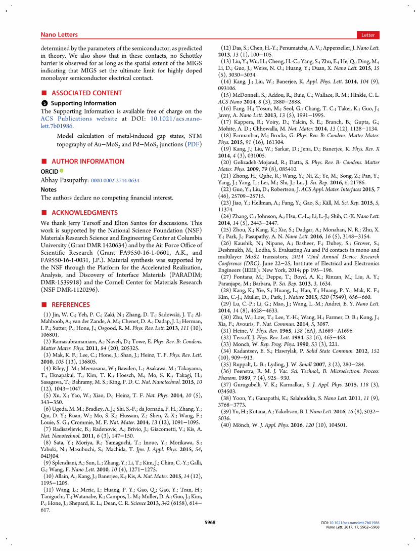
junction by analyzing a short spatial dI/dV profile across thejunction. Figure 3a shows a color map of the dI/dV calculatedfrom a ∼9 nm STS line scan of across the junction with theconcurrently measured sample-probe displacement. The sample-probe displacement shows that the contact edge is rounded forseveral nanometers which we primarily attribute to real physicalrounding of the imperfect step edges. We have verified this by
Figure 3. (a−c) Color maps of short (∼9 nm) dI/dV line profiles taken across the (a) graphite−MoS2, (b) Au−MoS2, and (c) Pd−MoS2 junctionsconsisting of 204 equally spaced points. Below the color map is a simultaneously measured STM topography profile revealing the approximate locationof the contact edge. The color map reveals a metallic L- DOS profile up until the edge of the electrode. Immediately to the right of the interface into theMoS2 side, there is still no observed L-DOS gap. A L-DOS gap emerges at a finite distance into the MoS2 side and grows for about 2 nm before reachingthe far from junction magnitude. (d) Individual dI/dV line spectra taken at 0, 0.5, 1, 1.5, and 2 nm from the junction, as shown by the dashed lines inpanel a. The individual line spectra confirm the apparent evolution seen in the color map, as the conduction and valence band edges are gradually definedwith distance from the junction, reaching the far from junction, full MoS2 band gap several nanometers from the junction.
Nano Letters Letter
DOI: 10.1021/acs.nanolett.7b01986Nano Lett. 2017, 17, 5962−5968
5965

obtaining consistent profiles with a variety of different STM tipscarefully prepared on Au(111). A comparison of line cuts takenwith different tips is also shown in the Supporting Information.We define the approximate junction position, the zero on ourplots, as where the sample-probe displacement flattens out tothat of the MoS2 layer, signifying that the STM probe isdefinitively tunneling only into MoS2. For analysis of effects inthe MoS2, this is a useful definition of the junction locationbecause it sets a clear boundary beyond which there is nopossibility that finite tip radius causes partial tunneling into themetal. Any uncertainty in location due to tip convolution wouldplace the real junction closer to the metal, not further, thus dataanalyzed beyond this position is not affected by finite tip radiusinteraction with themetal. Continuing to analyze the dI/dV colormap in Figure 3a, while the probe is above the graphite the colormap shows that the electronic spectra remain metallic, similar tothe graphite region observed in the long dI/dV line profile inFigure 2a. Once the probe crosses onto purely MoS2, a finite gapbegins to grow over the next 2 nm. This can be seen as both thevalence and conduction band edges begin near 0 V and gradually
shift toward their long-rangeMoS2 film values, observed earlier inFigure 2a. No clear band-bending and depletion region isobserved in our measurements. Color maps of Au−MoS2 andPd−MoS2 junctions in Figure 3b,c reveal the same behavior. Toensure that this effect is not a color map/plotting artifact, Figure3d shows several individual dI/dVs at different spatial positionsin the region of the evolution from the graphite−MoS2 interface.Comparing the dI/dVs, we see a gradual formation of the valenceband edge based on the negative voltage tails, which beginmetallic and gradually become more and more flat, approachingthe profile seen earlier in Figure 2b. We can also see theconduction band edge forming, althoughmasked by its proximityto the Fermi level. Thus, the L-DOS profiles show that the dI/dVgap grows with increasing distance from the edge of thegraphite−MoS2 junction. The same effect is observed in Au−MoS2 and Pd−MoS2 on similar length scales, as can be verified byFigure 3b,c.We find that the observations are best explained by the
continuum of metal-induced gap states (MIGS).31,32 Heineshowed that the presence of metal at the interface creates
Figure 4. (a) The band structure calculated in the simple model used to predict the MIGS decay lengths. The red curves show the real wave vectors, k,obtained for electrons in a 1D periodic potential, producing a band gap at the Brillioun zone boundary. The blue curve demonstrates the virtual states forimaginary k values (q = ik) within the band gap of the semiconductor, which characterize the MIGS decay lengths. In this simple model, the maximum qand minimum decay length (where δ = 1/q) are at mid gap while, at the band edges, q approaches 0 which leads to divergent decay lengths. (b) Plot ofthe experimental MIGS decay lengths into MoS2 calculated from linear fits at each energy for Pd−MoS2, Au−MoS2, and graphite−MoS2 junctions. Thetheoretical curve, derived from a 1D periodic potential model, is also plotted for reference. The experimental minimum decay length is about 0.55 nm atan energy slightly shifted toward the conduction band minimum from midgap due to the CNL shift from midgap in MoS2. The inset shows severalexample spatial L-DOS profiles at fixed voltages (from top to bottom,−1.98,−1.62,−1.26,−0.90,−0.54,−0.18 V), plotted on log scale, confirming thelinearity, hence the exponential behavior of theMIGS. (c) Energy band diagram for an ideal metal−semiconductor Schottky barrier, as well as theMIGSdecay lengths scaled longer than the characteristic band bending depletion width demonstrating why experimental results do not exhibit a Schottkybarrier.
Nano Letters Letter
DOI: 10.1021/acs.nanolett.7b01986Nano Lett. 2017, 17, 5962−5968
5966

evanescent states inside the semiconductor band gap whichdecay exponentially from the junction. These tailing states couldbe visualized as virtual gap states of the complex band structure ofthe semiconductor as shown in Figure 4a. For states that liewithin the band gap, only the imaginary part of wavevector kexists, resulting in exponential decay characterized by the decay
length, δ =q1 , where q = ik and k is the standard plane wave
vector. Monch developed a one-dimensional virtual gap statemodel to quantify this virtual gap state decay length (SupportingInformation).33 The model reveals that as a function of energythe decay lengths diverge at the band edges, whereas the decaylengths are minimum at the charge neutrality level (CNL), asplotted in Figure 4b. The CNL is at the center of the band gap inthis model but shifts when effective electron and hole masseshave any mismatch, which is the case of MoS2. The minimum
wave function decay length in this model is δ = πℏm aEmin2 2
e g, where ℏ
is the Planck constant,me is the free electron mass, a is the latticeconstant, and Eg is the semiconductor band gap. The decaylength of the L-DOS is half the value of the wave function decaylength, as the charge density is proportional to the wave functionsquared. Using the experimental values of in-plane latticeconstant a = 0.32 nm and single particle band gap Eg = 2.1 eVfor monolayer MoS2, the theoretical minimum decay length formetal−MoS2 interfaces is 0.36 nm.To confirm the presence of MIGS, we investigate the spatial
evolution of the MoS2 dI/dVs within the gap. The inset of Figure4b shows the logarithm of dI/dV intensity at a series of fixedenergies within the band gap, as a function of distance from thegraphite−MoS2 interface. The linear decrease in log(dI/dV) withdistance from the junction signifies the exponential decay of theMIGS in confirmation with theory. Linear regression fits onposition versus log(dI/dV) at each voltage within the band gapallow determination of the experimentally observed decay lengthof the MIGS. It is important to keep in mind that determinationof these exponential decay lengths does not require the ability toprobe the precise junction edge thus is not inhibited by tipconvolution. Figure 4b shows the experimental decay lengths as afunction of energy for the three different metal−MoS2 junctions,Au−MoS2, Pd−MoS2 and graphite−MoS2, as well as the decaylengths predicted by the previously mentioned theoretical model.The MIGS decay lengths for the three contact metals are almostidentical, as the decay length is determined solely by semi-conductor parameters, as in Monch’s model (SupportingInformation). The minimum decay length of 0.55 ± 0.10 nmoccurs around −0.6 V, slightly shifted toward the conductionband edge from midgap. This experimental decay length is quiteclose to the theoretical expectation of 0.36 nm, considering thesimplicity of the model that only accounted for the effect of theperiodic potential of the lattice. The shift of the minimum decaylength in energy from midgap is due to the mismatch in theeffective electron and hole masses in MoS2,
34 which shifts theCNL frommidgap. It has been found that the CNL in monolayerMoS2 is shifted toward the conduction band,22 the samedirection as the shift in minimum decay length in ourexperimental results. At the conduction band edge, we observethe expected divergence in the MIGS decay lengths, inconcurrence with the theoretical curve. Approaching the valenceband edge, there is a gradual increase in decay length, althoughthe MIGS persist into the valence band before diverging. Thiscontinuation of MIGS into the valence band, in disagreementwith models, has been previously observed.35 The inability of the
simple model to capture this effect is likely because the modelfails to account for the precise nature of the valence band and thelocalization of carriers near the valence band edge, which isaffected by defects and film quality. MIGS have beenexperimentally observed in 1D35 and 3D36 systems but to ourknowledge this is the first experimental confirmation of MIGS in2D materials.Additionally, it is interesting that no Schottky barrier behavior
is observed. Schottky barriers are normally characterized byspatial band-bending inside the semiconductor which indicatesthe depletion region inherent due to Fermi level misalignmentbetween the metal and semiconductor, as shown in Figure 4c.This is clearly not observed in our experimental dI/dV spatial lineprofiles implying that if there is any Schottky barrier, it is withinseveral angstroms of the real junction where we cannot resolve itor is concealed in the MIGS spatial extent, as depicted in Figure4c. Thus, in these highly doped monolayer semiconductors,MIGS set the ultimate limit for electrical contact. This shortupper limit on the depletion width is due to the large effectivesheet concentration of our MoS2 film, which we can estimate byemploying an analytic model for 2D depletion width (w2D) given
by Gurugubelli et al., where = ϕπ
ϵ −w
V
qN2D4 ( )eff bi
2D.37,38 Here,ϵeff is
effective dielectric constant, ϕbi is the built-in potential, V is theapplied bias, q is the elementary charge, and N2D is the effectivesheet carrier concentration. As opposed to the standard 3Dmodel, the 2Dmodel is suited for systems with 2Dmaterials suchas our metal−MoS2 junctions as it considers the role of thesignificant out-of-plane electric field which is absent in 3Dmodel.39 On the basis of the MIGS spatial extent and the tipconvolution uncertainty, we can assume a depletion widthshorter than 1.5 nm. This implies a lower limit on the effectivesheet carrier concentration using the 2D depletion width modelof at least∼1013 Carriers/cm2, a reasonable carrier concentrationfor degenerate n-type MoS2 films.16 We also find that theapplication of a back gate voltage from −20 to 80 V(corresponding to a sheet carrier density of 5 × 10¹² Carriers/cm2) does not significantly shift the dI/dV spectrum, furtherverifying this degenerate carrier concentration. This agrees withour previously mentioned findings that the MoS2 film has a highcarrier concentration due to the presence of band tails in theDOS. Future investigations of MoS2 and other TMDC samplesthat are more intrinsic will further the understanding of contactsby allowing direct observations of the Schottky barrier, depletionwidth, and MIGS, which can be used to compare metals, studygate dependence, and investigate novel methods to avoid Fermilevel pinning (which has in the past been attributed to MIGS).40
In conclusion, we investigated the metal−MoS2 junction ofthree different top contacts, graphite, Au, and Pd, on heavily n-type monolayer MOCVD grown MoS2 using UHV-STM andSTS. By fabricating clean nanoscale sharp contact edges on largeareaMoS2 films atop SiO2, we have provided subnanometer-scalespatial spectroscopic characterization of the evolution of the dI/dV, proportional to the L-DOS, of the MoS2 in the nanoscalevicinity of all three metal−MoS2 junctions. dI/dV line profilesacross the junctions reveal a gradually growing L-DOS gap in theMoS2, originating at the metal−MoS2 junction. The effect isattributed toMIGS originating from the contact metals, decayinginto the MoS2. By analyzing the energy dependence of the decaylength of the MIGS, we observe the decay length can vary from aminimum of 0.55 ± 0.10 nm to greater than 1 nm near the bandedges, in good agreement with theory. The MIGS decay length isshown to be independent of the contact metal and solely
Nano Letters Letter
DOI: 10.1021/acs.nanolett.7b01986Nano Lett. 2017, 17, 5962−5968
5967
determined by the parameters of the semiconductor, as predictedin theory. We also show that in these contacts, no Schottkybarrier is observed for as long as the spatial extent of the MIGSindicating that MIGS set the ultimate limit for highly dopedmonolayer semiconductor electrical contact.
■ ASSOCIATED CONTENT*S Supporting InformationThe Supporting Information is available free of charge on theACS Publications website at DOI: 10.1021/acs.nano-lett.7b01986.
Model calculation of metal-induced gap states, STMtopography of Au−MoS2 and Pd−MoS2 junctions (PDF)
■ AUTHOR INFORMATIONORCIDAbhay Pasupathy: 0000-0002-2744-0634NotesThe authors declare no competing financial interest.
■ ACKNOWLEDGMENTSWe thank Jerry Tersoff and Elton Santos for discussions. Thiswork is supported by the National Science Foundation (NSF)Materials Research Science and Engineering Center at ColumbiaUniversity (Grant DMR 1420634) and by the Air Force Office ofScientific Research (Grant FA9550-16-1-0601, A.K., andFA9550-16-1-0031, J.P.). Material synthesis was supported bythe NSF through the Platform for the Accelerated Realization,Analysis, and Discovery of Interface Materials (PARADIM;DMR-1539918) and the Cornell Center for Materials Research(NSF DMR-1120296).
■ REFERENCES(1) Jin, W. C.; Yeh, P. C.; Zaki, N.; Zhang, D. T.; Sadowski, J. T.; Al-Mahboob, A.; van der Zande, A.M.; Chenet, D. A.; Dadap, J. I.; Herman,I. P.; Sutter, P.; Hone, J.; Osgood, R. M. Phys. Rev. Lett. 2013, 111 (10),106801.(2) Ramasubramaniam, A.; Naveh, D.; Towe, E. Phys. Rev. B: Condens.Matter Mater. Phys. 2011, 84 (20), 205325.(3) Mak, K. F.; Lee, C.; Hone, J.; Shan, J.; Heinz, T. F. Phys. Rev. Lett.2010, 105 (13), 136805.(4) Riley, J. M.; Meevasana, W.; Bawden, L.; Asakawa, M.; Takayama,T.; Eknapakul, T.; Kim, T. K.; Hoesch, M.; Mo, S. K.; Takagi, H.;Sasagawa, T.; Bahramy, M. S.; King, P. D. C.Nat. Nanotechnol. 2015, 10(12), 1043−1047.(5) Xu, X.; Yao, W.; Xiao, D.; Heinz, T. F. Nat. Phys. 2014, 10 (5),343−350.(6) Ugeda, M.M.; Bradley, A. J.; Shi, S.-F.; da Jornada, F. H.; Zhang, Y.;Qiu, D. Y.; Ruan, W.; Mo, S.-K.; Hussain, Z.; Shen, Z.-X.; Wang, F.;Louie, S. G.; Crommie, M. F. Nat. Mater. 2014, 13 (12), 1091−1095.(7) Radisavljevic, B.; Radenovic, A.; Brivio, J.; Giacometti, V.; Kis, A.Nat. Nanotechnol. 2011, 6 (3), 147−150.(8) Sata, Y.; Moriya, R.; Yamaguchi, T.; Inoue, Y.; Morikawa, S.;Yabuki, N.; Masubuchi, S.; Machida, T. Jpn. J. Appl. Phys. 2015, 54,04DJ04.(9) Splendiani, A.; Sun, L.; Zhang, Y.; Li, T.; Kim, J.; Chim, C.-Y.; Galli,G.; Wang, F. Nano Lett. 2010, 10 (4), 1271−1275.(10) Allain, A.; Kang, J.; Banerjee, K.; Kis, A.Nat. Mater. 2015, 14 (12),1195−1205.(11) Wang, L.; Meric, I.; Huang, P. Y.; Gao, Q.; Gao, Y.; Tran, H.;Taniguchi, T.;Watanabe, K.; Campos, L.M.;Muller, D. A.; Guo, J.; Kim,P.; Hone, J.; Shepard, K. L.; Dean, C. R. Science 2013, 342 (6158), 614−617.
(12) Das, S.; Chen, H.-Y.; Penumatcha, A. V.; Appenzeller, J.Nano Lett.2013, 13 (1), 100−105.(13) Liu, Y.; Wu, H.; Cheng, H.-C.; Yang, S.; Zhu, E.; He, Q.; Ding, M.;Li, D.; Guo, J.; Weiss, N. O.; Huang, Y.; Duan, X. Nano Lett. 2015, 15(5), 3030−3034.(14) Kang, J.; Liu, W.; Banerjee, K. Appl. Phys. Lett. 2014, 104 (9),093106.(15) McDonnell, S.; Addou, R.; Buie, C.; Wallace, R. M.; Hinkle, C. L.ACS Nano 2014, 8 (3), 2880−2888.(16) Fang, H.; Tosun, M.; Seol, G.; Chang, T. C.; Takei, K.; Guo, J.;Javey, A. Nano Lett. 2013, 13 (5), 1991−1995.(17) Kappera, R.; Voiry, D.; Yalcin, S. E.; Branch, B.; Gupta, G.;Mohite, A. D.; Chhowalla, M. Nat. Mater. 2014, 13 (12), 1128−1134.(18) Farmanbar, M.; Brocks, G. Phys. Rev. B: Condens. Matter Mater.Phys. 2015, 91 (16), 161304.(19) Kang, J.; Liu, W.; Sarkar, D.; Jena, D.; Banerjee, K. Phys. Rev. X2014, 4 (3), 031005.(20) Golizadeh-Mojarad, R.; Datta, S. Phys. Rev. B: Condens. MatterMater. Phys. 2009, 79 (8), 085410.(21) Zhong, H.; Quhe, R.; Wang, Y.; Ni, Z.; Ye, M.; Song, Z.; Pan, Y.;Yang, J.; Yang, L.; Lei, M.; Shi, J.; Lu, J. Sci. Rep. 2016, 6, 21786.(22) Guo, Y.; Liu, D.; Robertson, J. ACS Appl. Mater. Interfaces 2015, 7(46), 25709−25715.(23) Jiao, Y.; Hellman, A.; Fang, Y.; Gao, S.; Kall, M. Sci. Rep. 2015, 5,11374.(24) Zhang, C.; Johnson, A.; Hsu, C.-L.; Li, L.-J.; Shih, C.-K.Nano Lett.2014, 14 (5), 2443−2447.(25) Zhou, X.; Kang, K.; Xie, S.; Dadgar, A.; Monahan, N. R.; Zhu, X.Y.; Park, J.; Pasupathy, A. N. Nano Lett. 2016, 16 (5), 3148−3154.(26) Kaushik, N.; Nipane, A.; Basheer, F.; Dubey, S.; Grover, S.;Deshmukh, M.; Lodha, S. Evaluating Au and Pd contacts in mono andmultilayer MoS2 transistors, 2014 72nd Annual Device ResearchConference (DRC), June 22−25, Institute of Electrical and ElectronicsEngineers (IEEE): New York, 2014; pp 195−196.(27) Fontana, M.; Deppe, T.; Boyd, A. K.; Rinzan, M.; Liu, A. Y.;Paranjape, M.; Barbara, P. Sci. Rep. 2013, 3, 1634.(28) Kang, K.; Xie, S.; Huang, L.; Han, Y.; Huang, P. Y.; Mak, K. F.;Kim, C.-J.; Muller, D.; Park, J. Nature 2015, 520 (7549), 656−660.(29) Lu, C.-P.; Li, G.; Mao, J.; Wang, L.-M.; Andrei, E. Y. Nano Lett.2014, 14 (8), 4628−4633.(30) Zhu, W.; Low, T.; Lee, Y.-H.; Wang, H.; Farmer, D. B.; Kong, J.;Xia, F.; Avouris, P. Nat. Commun. 2014, 5, 3087.(31) Heine, V. Phys. Rev. 1965, 138 (6A), A1689−A1696.(32) Tersoff, J. Phys. Rev. Lett. 1984, 52 (6), 465−468.(33) Monch, W. Rep. Prog. Phys. 1990, 53 (3), 221.(34) Kadantsev, E. S.; Hawrylak, P. Solid State Commun. 2012, 152(10), 909−913.(35) Ruppalt, L. B.; Lyding, J. W. Small 2007, 3 (2), 280−284.(36) Feenstra, R. M. J. Vac. Sci. Technol., B: Microelectron. Process.Phenom. 1989, 7 (4), 925−930.(37) Gurugubelli, V. K.; Karmalkar, S. J. Appl. Phys. 2015, 118 (3),034503.(38) Yoon, Y.; Ganapathi, K.; Salahuddin, S. Nano Lett. 2011, 11 (9),3768−3773.(39) Yu, H.; Kutana, A.; Yakobson, B. I.Nano Lett. 2016, 16 (8), 5032−5036.(40) Monch, W. J. Appl. Phys. 2016, 120 (10), 104501.
Nano Letters Letter
DOI: 10.1021/acs.nanolett.7b01986Nano Lett. 2017, 17, 5962−5968
5968