Embed Size (px)
Citation preview

ISL78600, ISL78610 - A Case Study
APPLICATION NOTE
AN1723Rev 0.00
July 6, 2016
AbstractThe design of a daisy chain battery system, while fairly straightforward, has a number of design elements that can become obstacles to implementation. This case study provides a glimpse into the questions and responses in the development of one daisy chain system.
Table of ContentsIntroduction . . . . . . . . . . . . . . . . . . . . . . . . . . . . . . . . . . . . . . . . . . . . . . . . . . . . . . . . . . . . . . . . . . . . . . . . . . . . . . . . . . . . . . . . . . . . . . . . 2
System Description . . . . . . . . . . . . . . . . . . . . . . . . . . . . . . . . . . . . . . . . . . . . . . . . . . . . . . . . . . . . . . . . . . . . . . . . . . . . . . . . . . . . . . . . . . 2
Questions and Answers . . . . . . . . . . . . . . . . . . . . . . . . . . . . . . . . . . . . . . . . . . . . . . . . . . . . . . . . . . . . . . . . . . . . . . . . . . . . . . . . . . . . . . 2Cell Input Accuracy . . . . . . . . . . . . . . . . . . . . . . . . . . . . . . . . . . . . . . . . . . . . . . . . . . . . . . . . . . . . . . . . . . . . . . . . . . . . . . . . . . . . . . . . . . . . . . . .2Cell Balancing. . . . . . . . . . . . . . . . . . . . . . . . . . . . . . . . . . . . . . . . . . . . . . . . . . . . . . . . . . . . . . . . . . . . . . . . . . . . . . . . . . . . . . . . . . . . . . . . . . . . .3CRC . . . . . . . . . . . . . . . . . . . . . . . . . . . . . . . . . . . . . . . . . . . . . . . . . . . . . . . . . . . . . . . . . . . . . . . . . . . . . . . . . . . . . . . . . . . . . . . . . . . . . . . . . . . . .5Daisy Chain Hardware. . . . . . . . . . . . . . . . . . . . . . . . . . . . . . . . . . . . . . . . . . . . . . . . . . . . . . . . . . . . . . . . . . . . . . . . . . . . . . . . . . . . . . . . . . . . . .7Communication Software. . . . . . . . . . . . . . . . . . . . . . . . . . . . . . . . . . . . . . . . . . . . . . . . . . . . . . . . . . . . . . . . . . . . . . . . . . . . . . . . . . . . . . . . . 11PCB Layout . . . . . . . . . . . . . . . . . . . . . . . . . . . . . . . . . . . . . . . . . . . . . . . . . . . . . . . . . . . . . . . . . . . . . . . . . . . . . . . . . . . . . . . . . . . . . . . . . . . . . 14
List of FiguresFIGURE 1. Initial VBAT Connection. . . . . . . . . . . . . . . . . . . . . . . . . . . . . . . . . . . . . . . . . . . . . . . . . . . . . . . . . . . . . . . . . . . . . . . . . . . . . . . . . . . . .2FIGURE 2. Simplified Cell Balance Circuit. . . . . . . . . . . . . . . . . . . . . . . . . . . . . . . . . . . . . . . . . . . . . . . . . . . . . . . . . . . . . . . . . . . . . . . . . . . . . . .4FIGURE 3. Illustration of Auto Balance . . . . . . . . . . . . . . . . . . . . . . . . . . . . . . . . . . . . . . . . . . . . . . . . . . . . . . . . . . . . . . . . . . . . . . . . . . . . . . . . .5FIGURE 4. Illustration of Auto Balance (Multiple Cells). . . . . . . . . . . . . . . . . . . . . . . . . . . . . . . . . . . . . . . . . . . . . . . . . . . . . . . . . . . . . . . . . . . .5FIGURE 5. Example CRC Calculation Routine (Visual Basic) . . . . . . . . . . . . . . . . . . . . . . . . . . . . . . . . . . . . . . . . . . . . . . . . . . . . . . . . . . . . . . .6FIGURE 6. Customer Original Daisy Chain Control Connections . . . . . . . . . . . . . . . . . . . . . . . . . . . . . . . . . . . . . . . . . . . . . . . . . . . . . . . . . . . .7FIGURE 7. Proper Daisy Chain Circuit for Single Board Connections . . . . . . . . . . . . . . . . . . . . . . . . . . . . . . . . . . . . . . . . . . . . . . . . . . . . . . . .8FIGURE 8. Customer Reported Correct Stand-Alone Communication . . . . . . . . . . . . . . . . . . . . . . . . . . . . . . . . . . . . . . . . . . . . . . . . . . . . . . .9FIGURE 9. Wake-Up Daisy Chain Signals . . . . . . . . . . . . . . . . . . . . . . . . . . . . . . . . . . . . . . . . . . . . . . . . . . . . . . . . . . . . . . . . . . . . . . . . . . . . . . .9FIGURE 10. Customer DHI/DLO Traces . . . . . . . . . . . . . . . . . . . . . . . . . . . . . . . . . . . . . . . . . . . . . . . . . . . . . . . . . . . . . . . . . . . . . . . . . . . . . . . . 10FIGURE 11. Recommended Daisy Connections Between Separate PCBS (Components Selected for 500kHz Data Rate) . . . . . . . . . . . 10FIGURE 12. Customer Daisy Waveforms after Changes (Good) . . . . . . . . . . . . . . . . . . . . . . . . . . . . . . . . . . . . . . . . . . . . . . . . . . . . . . . . . . . . 11FIGURE 13. Customer Base ID Command (SPI) . . . . . . . . . . . . . . . . . . . . . . . . . . . . . . . . . . . . . . . . . . . . . . . . . . . . . . . . . . . . . . . . . . . . . . . . . 12FIGURE 14. Customer Data Ready Response Handling Timing . . . . . . . . . . . . . . . . . . . . . . . . . . . . . . . . . . . . . . . . . . . . . . . . . . . . . . . . . . . . 12FIGURE 15. Example Identification Sequence from Intersil (Good Responses) . . . . . . . . . . . . . . . . . . . . . . . . . . . . . . . . . . . . . . . . . . . . . . . 13
AN1723 Rev 0.00 Page 1 of 15July 6, 2016
ISL78600, ISL78610 - A Case Study
IntroductionThe ISL78600 and ISL78610 are Li-ion battery manager ICs that supervise up to 12 series connected cells. The parts perform accurate monitoring, cell balancing and extensive system diagnostics functions. The devices communicate to a host microcontroller via an SPI interface and to other ISL78600, ISL78610 devices using a robust, proprietary, 2-wire daisy chain system.
The ISL78600 and ISL78610 operate identically. So, aside from cell measurement accuracy in which the ISL78600 has more accurate cell measurement, references to the ISL78600 in this document also apply to the ISL78610.
The information in this study is taken from an actual design, however, specifics of the design have been substituted to preserve the proprietary aspects of the customer’s design. Also, the customer questions and responses have been only marginally “cleaned up”. There are many cases in which the responses to questions lead to more questions, as is typically the case in debugging a system. Including these responses is intended to improve the insight into the philosophy of the design to lead to more “intuitive” understanding of the system.
System DescriptionThe system in this case study consists of multiple ISL78600 devices operating in a daisy chain configuration. Each IC manages between 7 and 12 cells and two ICs work together to make a module of 14 to 24 cells. These modules connect together to support packs with up to 4 modules (56 cells to 96 cells.) The initial definition of the system (as presented by the designer) did not clearly state whether there was a single board or a connection of multiple modules. It also did not specify the cell voltages.
Questions and AnswersCell Input Accuracy
QUESTION 1We started by testing the ISL78600 in a stand-alone configuration and experienced an unknown failure with the ISL78600. The part was working fine and then we started getting undervoltage faults. I looked at the cell voltage measurements and the part is seeing the following voltages on each cell:
Cell 1 = 3.271V
Cell 2 = 3.115V
Cell 3 = 2.932V
Cell 4 = 3.246V
Cell 5 = 3.304V
Cell 6 = 3.309V
Cell 7 = 3.305V
Cell 8 = 3.301V
Cell 9 = 3.310V
Cell 10 = 3.300V
Cell 11 = 3.306V
Cell 12 = 3.306VThe problem is that when I measured the cells with a multimeter, all cells measured ~3.3V. I also measured the voltage at the input pins of the IC and the voltage measures ~3.3V. However, for Cell 3, the part reports a voltage of 2.932V.
Can you explain this failure? Also, can you confirm that (4) of the cell analog voltage measurements failing is not merely a coincidence, but likely a result of the architecture (i.e., the 12 cells are measured with 3 A/D converters each fed from a 4-input multiplexer and a multiplexer has failed)?
ANSWER 2There is only one A/D, so the problem is due to something else. One thing to check is if the series resistor on VBAT is still OK. If it is physically too small (0603), then it can be damaged when the VBAT input cap is initially charged. This can affect the power supply of the part and may affect readings. This input resistor should be at least an 0805 size resistor.
QUESTION 2The VBAT input resistor was not damaged. Attached is a schematic of the VBAT connection.
ANSWER 2Normally, we recommend a 27Ω resistor. While a 47Ω resistor may be OK, what happens is that the voltage at the VBAT pin drops when there is higher current, like during SPI or daisy chain communications. If the voltage drops too much, then there is not enough headroom on the front end analog circuits and there can be measurement errors. So, if the input resistor is not damaged then try a 27Ω resistor to see if this makes a difference.
If a smaller resistor value does not make a difference, then check that there is no large voltage differential across the VBAT series resistor. There should be a small drop in voltage (up to about 80mV), however, if there is more than this, check the diode. If the diode is OK and there is still a voltage drop across the resistor, then the part may be damaged.
The schematic shows two connections to the top of the stack, one for VBAT and one for VC12. This is OK, however, check to see
FIGURE 1. INITIAL VBAT CONNECTION
VBAT
VC12
60V
BATsenB
BATsenA1k
100n
47 (27)
220n
(1µF)
(22nF)
GND
GNDBLACK: ORIGINAL
RED: RECOMMENDED
AN1723 Rev 0.00 Page 2 of 15July 6, 2016

ISL78600, ISL78610 - A Case Study
if there is a fault condition. If the BATsenB wire is broken, it could affect the measurement accuracy, however, this would also show up as an open VBAT fault.
One other thing to check, if there is an accuracy error, is the MISR checksum to see if there has been any changes to the EEPROM or a problem reading the EEPROM. Do this by seeing that the EEPROM CALC value matches the EEPROM MISR value. If they do not match, it indicates that the part might be damaged. If this is the case, please let us know so we can follow up with a Failure Analysis.
Another recommendation we make on the input filters is that the time constants on all inputs be the same (or about the same). In this case, the cell input time constant is about 16 times the VBAT time constant. If there are high voltage transients on the pack voltage, the differential time constants will result in high voltage differentials on the IC input pins. To minimize this, we recommend different filter values, as shown in RED in Figure 1 on page 2.
Cell Balancing
QUESTION 3In the ISL78600 application circuit there are three P-channel FETs and nine N-channel FETs. What is the reason for using different FET types in the Cell Balance circuit? Can we use N-channel FETs for all cells?
ANSWER 3We require N-channel devices on the bottom cells, because we supply a current out of the device from VBAT to turn on the FETs. On the upper side, we require P-channel devices, because we supply a current into the device to GND to turn on the FETs. If we had specified the use of all N-channel devices, then we would have required an internal charge pump to turn on the upper FETs. Or, we could have powered the cell balance FETs from the cell being balanced. However, we think our approach has the following advantages:
• By using currents from the top or bottom rail, the device is more immune to hot plug issues.
• By driving the FETs in the way we do, the FET drive voltages can be 8V, instead of as low as 2V, regardless of the battery cell voltage. This lets the FETs be driven harder.
• With our FET drive technique, there is less likelihood that the FETs will turn on due to RF or other noise in the system, because FETs with higher turn-on threshold can be used.
• The ISL78600 does not need a charge pump to drive the upper cell balance FETs.
QUESTION 4In manual balance mode, with the Balance Setup register set to 0x001, I enabled balancing by writing 0x201 to the Balance Setup register. This works fine and the cells balance under the control of my firmware except under one condition when a large current is drawn from the battery. When this happens, I read the Balance Setup register and the value is 0x001, which means that the large current event effectively disabled the balancing. The ISL78600 does not re-enable balancing after the large current event, so I must do so. I believe this effect is just the FETs turning
off, but I wanted to check if the ISL78600 is actively doing something here.
ANSWER 4In most systems we see, cell balancing is done during charge, so cell balance stopping during a large current event has not typically been an issue. However, a transient event may be causing a Power-On Reset (POR). This would cause the memory to be reloaded from EEPROM. The way to see if this is causing the problem is to check if other bits are reset in addition to the balance setup. (Before the test, set some unrelated, unused bit and see if it also is reset.)
Looking at this in a little more detail, simulations of the device show that if the VBAT voltage sees a 10V step down in 5µs, the device issues a POR. It is possible that when a large current is drawn from the battery, the VBAT voltage experiences this characteristic input “glitch”. If the device power-on reset circuit is triggered by this glitch, the device resets the register values, including those controlling the Cell Balance values.
From board testing, a VBAT voltage drop of 20V (for example, from 48V to 28V), a 100µs wide glitch will marginally cause the fault condition.
With VBAT voltage drop of 10V (for example, from 48V to 38V), a 40µs wide glitch may cause the fault condition.
We have demonstrated that this condition can be prevented by adding additional filtering to the VBAT pin.
Note: Follow-up with design identified this glitch sensitivity as a limitation in the IC. A design change eliminated this sensitivity in the latest revision of the silicon, released in 2016. See Intersil PCN16033.
Other than this input glitch causing a POR, cell balancing can be turned off in balance mode in the following ways:
1. The Watchdog timer times out. If the µC stops sending commands to the device, then the WDT expires, balancing stops and the device goes to sleep.
2. The sleep mode bit is set.
3. The EN bit is toggled. This is like a POR.
4. The voltage on the VBAT pin drops below about 4.4V. This causes a normal power-on reset where the registers are reloaded with the default values.
5. If the device detects an undervoltage condition, balancing is turned off. This requires a voltage scan to detect the undervoltage condition, either a µC initiated command or scan continuous.
QUESTION 5I am still trying to get to the bottom of this, but perhaps the following additional observation explains the behavior, because it occurs when none of the above scenarios suggested occur.
Under no-load on the batteries, when one or more of the cells measures <3.2V, if I write the cells to be balanced to the Balance Status register, then attempt to write 0x201 to the Balance Setup register to enable balancing and turn on the corresponding FETs, balancing is not enabled. Due to the delay in my readback of the registers, I don't know if Balance Setup gets set to 0x201 and is
AN1723 Rev 0.00 Page 3 of 15July 6, 2016

ISL78600, ISL78610 - A Case Study
then disabled to 0x001, or if it never gets set at all because of a condition that I am not aware of. As soon as all the cells measure >3.2V, I can send the same commands and the Balance Setup registers reads back 0x201 indicating that balancing is enabled.
As you know, a unique feature of LiFePO4 cells is that they can handle 30C discharge currents, so when we draw even 40A from a 2.5Ah cell with 8-12mΩ series resistance, the voltage per cell easily drops below 3.2V. My question is, “Is there an internal function on the ISL78600 that prevents balancing below a certain voltage?” Because that may explain both situations - (1) the inability to enable balancing under no load conditions with any cell <3.2V and (2) the disabling of balancing under high load currents when the cell voltages collectively drop below 3.2V.
To help understand our implementation, the relevant register settings are shown in Table 1.
Balance Setup (0x1) is programmed for manual balance mode, where my host MCU is manually reading the cell voltages and turning on the cells that need to be balanced. The problem is that when either (1) any one of the cells are below ~3.2V or (2) high current draws bring the cell voltage down, likely below 3.2V, the Balance Setup register cannot be written to 0x201, and if it is, it gets changed to 0x1 as shown.
ANSWER 5There is no inherent limit for cell balance other than those already discussed. We have tested this on our evaluation board and were unable to duplicate the inability to set the balance condition with cell voltages below 3.2V as you describe above.
Note: Much later (after most other issues were resolved,) the customer responded with the following statement:
I have not seen the inability to balance at low voltage issue anymore. Interestingly, when I dove deeper into this issue, the gate of the balancing FET was being turned on and then going off. I am pretty sure this issue hasn't appeared since I sped up my clock (See “ANSWER 13” on page 13,) which might lead to something else interesting, but on this one, I am not certain that the clock speed was the only thing that changed.
QUESTION 6I was looking at the automatic cell balance operation. How does it work?
ANSWER 6The ISL78600 Auto Balancing system removes a specific amount of charge from each cell. It does not balance to a voltage. To use the auto balance system one must know the amount of charge required to be removed from each cell. This is normally established by calculating the State of Charge (SOC) of each cell and then calculating the amount of charge to be removed from each cell so that the pack becomes balanced.
The calculation of the SOC is left to the system designer. This value is highly dependent on the cell chemistry, discharge/charge rates, temperature, age of the cells and a number of other factors.
Once the amount of charge to be removed is known, all that is needed is the total resistance of the balancing circuit, which is normally the sum of the balance resistor value and the ON-resistance of the balancing FET, and the time for which balancing is enabled for each cycle, the “Balance Time”. These figures are then used to calculate a “Balance Value,” B, which is used by the ISL78600 to control the balancing process. The derivation of Balance Value is shown below.
A simple circuit showing a cell and balancing components is shown in Figure 2.
In Figure 2 cell voltage is given by V, balance circuit resistance by R and balance current by I. The relationship of these terms is then:
The total amount of charge, Q, removed during balancing for a period t seconds is then given by:
When using Auto Balance mode, the ISL78600 balances using fixed “Balance Time” periods, such that a number of these periods will be required to balance for the full time, t, given in Equation 2. Using T to represent Balance Time and n to represent number of periods, Equation 2 can be rewritten:
TABLE 1. CUSTOMER SYSTEM REGISTER SETTINGS
REGISTER SETTING COMMENTS
Fault Setup 0x0160 Internal temp enabled 8 sample totalizer 16ms scan interval
Fault Status 0x0000
Overvoltage Limit 0x17AE 3.7V
Undervoltage Limit 0x0CCE 2V
Internal Temperature Limit 0x3482
External Temperature Limit 0x1FFF No external thermistors yet
Balance Setup 0x0001 Manual balance
Balance Status 0x0555 Balance odd cells
Watchdog/Balance Time 0x007F WDT timeout = 128 minutes
Comms Setup 0x0000
Device Setup 0x000B
FIGURE 2. SIMPLIFIED CELL BALANCE CIRCUIT
I RV
IVR----= (EQ. 1)
Q I t VR---- t= = (EQ. 2)
QVR---- T n= (EQ. 3)
AN1723 Rev 0.00 Page 4 of 15July 6, 2016

ISL78600, ISL78610 - A Case Study
In Equation 3, the values of Q, R and T are known. Only V and n are unknown. Equation 3 can be rearranged in terms of the unknown values as follows:
Equation 4 tells us that if we apply balancing to a cell with voltage V for a total of n cycles then we will complete balancing with the required amount of charge, Q, removed from the cell. The ISL78600 uses the expression V x n as the balance value and deducts the cell voltage V at the end of each Balance Time. In this manner, the ISL78600 applies n balancing cycles to the cell before completing the Auto Balance routine.
There is a slight modification required to Equation 4 when using this with the ISL78600. The ISL78600 uses the ADC conversion value of cell voltage, so we must scale the expression of Equation 4 accordingly. The scaling factor applied is 8192/5. So Equation 4 becomes:
The Balance Value is calculated for each cell to be balanced. The ISL78600 then balances each cell, subtracting the measured cell voltage from the Balance Value at the end of each Balance Time interval, until the Balance Value is zero. See Figures 3 and 4. QUESTION 7
I do not understand how to get 15 cycles in the automatic balance mode example in the datasheet.
ANSWER 7The total coulomb difference to be balanced is: 470 coulomb (9360 - 8890). Therefore, 3.3V / 31Ω * 300s = 31.9 coulomb/cycle, and it will take 15 cycles for the balancing to be finished.
CRC
QUESTION 8Do you have any further documentation, application notes, or sample code on the 4-bit CRC used in the daisy chain mode of the ISL78600? I am trying to get the daisy chain system working for the first time and I am having a couple of issues with the checksum.
ANSWER 8The CRC routine used in the ISL78600 GUI is shown in Figure 5.FIGURE 3. ILLUSTRATION OF AUTO BALANCE
V n Q R T
--------------------= (EQ. 4)
V ADC n Q R T
-------------------- 81925
------------- BalanceValue= = (EQ. 5)
B
Celln Cellx Cellx Cellx Cellx
I x t I x t
SOC
PERIOD 1 2
I x t
n
- Determine amount of excess capacity in CELLx than in CELLn- Remove part of the excess capacity in each cycle- Continue until the excess capacity is removed
RECALCULATE
FIGURE 4. ILLUSTRATION OF AUTO BALANCE (MULTIPLE CELLS)
- Each period capacity is removed from cells- When all capacity is removed from a cell, balance for that cell ends- Balance continues on remaining cells until excess capacity is
1
3
4
2
5
1
3
4
2
5
1
3
4
2
5
PERIOD 1 PERIOD 2 PERIOD (n-1)
removed from all cells.
AN1723 Rev 0.00 Page 5 of 15July 6, 2016

ISL78600, ISL78610 - A Case Study
FIGURE 5. EXAMPLE CRC CALCULATION ROUTINE (VISUAL BASIC)
Attribute VB_Name = "isl78600evb_crc4_lib"' File - isl78600evb_crc4_lib.bas' Copyright (c) 2010 Intersil' -----------------------------------------------------------------------------Option Explicit'***********************************************************' CRC4 Routines'***********************************************************Public Function CheckCRC4(myArray() As Byte) As Boolean
'returns True if CRC4 checksum (low nibble of last byte in myarray) 'is good. Array can be any length Dim crc4 As Byte
Dim lastnibble As Byte lastnibble = myArray(UBound(myArray)) And &HF crc4 = CalculateCRC4(myArray) If lastnibble = crc4 Then
CheckCRC4 = True Else
CheckCRC4 = False End If
End Function
Public Sub AddCRC4(myArray() As Byte) 'adds CRC4 checksum (low nibble in last byte in array) 'array can be any length Dim crc4 As Byte crc4 = CalculateCRC4(myArray) myArray(UBound(myArray)) = (myArray(UBound(myArray)) And &HF0) Or
crc4
End Sub
Public Function CalculateCRC4(ByRef myArray() As Byte) As Byte 'calculates/returns the CRC4 checksum of array contents excluding 'last low nibble. Array can be any length
Dim size As Integer Dim i As Integer Dim j As Integer Dim k As Integer Dim bit0 As Boolean, bit1 As Boolean, bit2 As Boolean, bit3 As Boolean Dim ff0 As Boolean, ff1 As Boolean, ff2 As Boolean, ff3 As Boolean Dim carry As Boolean Dim arraycopy() As Byte Dim result As Byte
'copy data so we do not clobber source array ReDim arraycopy(LBound(myArray) To UBound(myArray)) As Byte For i = LBound(myArray) To UBound(myArray)
arraycopy(i) = myArray(i) Next
'initialize bits bit0 = False bit1 = False bit2 = False bit3 = False 'simple implementation of CRC4 (using polynomial 1 + X + X^4)
For i = LBound(arraycopy) To UBound(arraycopy) 'last nibble is ignored for CRC4 calculations If i = UBound(arraycopy) Then
k = 4 Else
k = 8 End If For j = 1 To k
'shift left one bit carry = (arraycopy(i) And &H80) > 0 arraycopy(i) = (arraycopy(i) And &H7F) * 2 'see ISL78600 datasheet, Fig 11: 4-bit CRC calculation ff0 = carry Xor bit3 ff1 = bit0 Xor bit3 ff2 = bit1 ff3 = bit2 bit0 = ff0 bit1 = ff1
bit2 = ff2 bit3 = ff3
Next jNext i 'combine bits to obtain CRC4 result result = 0 If bit0 Then
result = result + 1 End If If bit1 Then
result = result + 2 End If If bit2 Then
result = result + 4 End If If bit3 Then
result = result + 8 End If CalculateCRC4 = result
End Function
AN1723 Rev 0.00 Page 6 of 15July 6, 2016

ISL78600, ISL78610 - A Case Study
Daisy Chain Hardware
QUESTION 9We are experiencing some difficulty getting the ISL78600 to start up in the Daisy Chain mode. I have two ISL78600 devices connected with:
• Master/bottom device set to CommsSel1 = 0, CommsSel2 = 1
• Top device set to CommsSel1 = 1, CommsSel2 = 0
• Both devices have CommsRate0 = 0, CommsRate1 = 1 for 125kHz daisy chain communication
On power-up, the part is automatically enabled with EN (Pin 47) = “1”.
Then, I attempt to send the base identify message as 0x032404.
I never see DATA READY go low and never get a response out of the part.
I believe that the fault status register has the OSC bit set, which is concerning but I don't understand why. Is the proper way to handle this situation described in the table “Summary of Diagnostics Commands and Responses” of the datasheet (Fault Diagnostics, Oscillator Check function, i.e., send repeated sleep and wake-up commands)? If so, could you elaborate on why this Sleep/Wake-up sequence is necessary?
ANSWER 9The following answer is from the customer posing the question.
I have an important clarification to make - upon further investigation of what I thought I was reading as an OSC fault, I realized that I am misinterpreting what is actually just a Comms Failure. When the Host MCU sends a command to read the Fault Status register, I am receiving 0x13380007 back from the master/bottom device, which my fault reading function was interpreting as an OSC fault but the function's response is not valid in the Daisy Chain mode. I verified this by looking at the FAULT pin which remains high, indicating that there is no actual fault occurring.
In summary, I am receiving Comms Failures from the master/bottom device and I am not clear how to properly initialize the daisy chain stack and get a valid Base Identify command to propagate through. I believe both the master/bottom and top devices are currently in some sort of sleep mode, based on the currents measured in my original email, but I cannot confirm this for sure. Any help here would be great.
In addition, the following comment is from Intersil:
The reason for the Sleep/Wake sequence is that the master will wake-up on any SPI command. However, if the master is already awake, it ignores the wake-up command. By sending a Sleep command to the master first, followed by the Wake-up command, you insure that the master starts off in sleep mode, so all devices in the system are ready for the wake-up sequence.
QUESTION 10Below (Figure 6) is a schematic of the ISL78600 daisy chain and control circuits in my battery management system.
Resistor R12 is not loaded and the Comms pull-up/pull-down resistors are loaded according to the configuration settings above. I measured the voltage across the resistor, R7, in the schematic. The master bottom device is currently reading 11.9mV (360µA) and the top device is currently reading 2.4mV (72µA). Neither of these currents are popping off the datasheet to tell me what is going on.
FIGURE 6. CUSTOMER ORIGINAL DAISY CHAIN CONTROL CONNECTIONS
DHI1_Top
DLO1_Top1k
1k
1000p
DHI2_M
DLO2_M
1000p
1000p
1000p
EN
R12
R7
1M
R131M
3.3V
GND
CommsRate 0
R91k
R51k
V3P3
GND
R101k
R61k
V3P3
GND
R111k
R71k
V3P3
GND
R81k
R41k
V3P3
GND
CommsRate 1
CommsSelect 1
CommsSelect 2
VBAT
33
BAT+
GND
470p
470p
V3P3
R142.2k
VBAT
GND
Base
V3P3
C8
C10
C7
C9
AN1723 Rev 0.00 Page 7 of 15July 6, 2016

ISL78600, ISL78610 - A Case Study
ANSWER 10The first thing to notice on the schematic is that the center point of the capacitors C8 and C10 (and C7 and C9) should be at the respective IC GND (see Figure 7).
If there is a cable between the two devices, then there should be a different arrangement of isolation components, though it will still work this way. The extra components are to protect the system in case of a cable short to chassis and to provide higher ESD immunity.
Is there any reason for running at 125kHz? Usually the slower speeds are only if the design calls for long cable lengths. Otherwise, we would think that the faster communication is preferred. (If the µC cannot respond fast enough, you may want to slow the daisy chain down.)
There are a couple of other changes that we recommend.
1. Resistor R14 is probably too big. This will work OK for stand-alone, however, because of higher currents in the Daisy Chain mode, it might cause the 3.3V supply to drop out during communications. In our designs, we use a 100Ω resistor.
2. On the V3P3 regulator, the collector resistor R14 is shown to connect to VBAT. This should connect to BAT+, otherwise the V3P3 current will also flow through R7, reducing the VBAT voltage.
The observation that current across R7 is only 360µA indicates that the device thinks it is a stand-alone device (i.e., Comms Select pins both at 0). Please check this.
QUESTION 11I connected the center-points of the AC coupling capacitors to their respective ground points. I can confirm now the following:
1. Board powers up, EN comes HIGH with 3.3V supply, DATA_READY is coming up HIGH on a clean power up. I can still toggle the DATA_READY default state by sending 0xFBFFFF (ISL78600 datasheet, “Communication Failure” section).
2. If I send the Sleep command, DATA_READY drops from 3.3V to ~2.9V.
3. If I send the Wake-up command, DATA_READY returns from ~2.9V to 3.3V.
4. If I send the Base Identify command (0x032404 clocked out on MOSI) with a ~2MHz SPI clock, I see no data on the MISO. By the way, I measured the timing between my SPI bytes and it's 35µs.
I tried triggering on a falling edge of DATA_READY or any transition on the two daisy chain lines, but I am seeing nothing. Do you have any suggestions for what I can look to next? My plan is to separate the master/bottom and top device, change the CommSelect resistors back to Non-Daisy Chain mode, and confirm non-daisy chain operation of the master ISL78600. Assuming everything looks healthy, I will be back to this point. Please let me know if there are any test sequences you know of that would be helpful.
ANSWER 11Since there are a number of issues, this answer is handled as a dialog. A: indicates the Intersil responses; Q: refers to the customer responses.
A: Trying to communicate with one IC as a “stand-alone” device is a good idea, to at least check that the SPI commands are getting to the first device and getting proper responses. In stand-alone mode, you do not need to do an identify procedure, you will not get DATA_READY, and commands and responses have one fewer byte.
Q: I was able to successfully communicate with the master/bottom device as a stand-alone device. I can read the formatted data out of the part and it looks exactly like I would expect it to, based on using a single ISL78600 in Stand-Alone mode in the past.
A: In the daisy chain configuration, when you send the sleep command and see the DATA_READY voltage going from 3.3V to 2.9V, check the V3P3 voltage on the top device to see if it also is changing. If it is not, then try sending the sleep/wake commands two times. If it is still not changing, then there is probably still something wrong with the daisy chain hardware.
Q: No, the V3P3 on the top device doesn't move when I send two sleep/wake-up commands.
A: Can you put a scope on the DHI2 and DLO2 pins and capture a command? Reference both probes to ground. You may need to add a large offset to the scope inputs. If the VBAT voltage is 20V, then the scope probe would need an offset of 10V (since the common-mode voltage on the daisy chain is VBAT/2).
Q: I see the 20V offset but I don't see any movement on the DHI2/DLO2 pins. This is probably why I am not seeing any activity on the top device V3P3 because no message is getting sent along the daisy chain if there is no activity on it.
What would cause the master device to accept sleep/wake-up but not send anything along the 2-wire daisy chain lines? Is a part failure the only explanation?
Figure 8 on page 9 shows the SPI Identify command. The MISO data looks like 0x070000 but that's nothing valid to the best of my knowledge. If I send this command a few times in a row, I can get the MISO data to be 0x133800, which looks like a Comms Failure to me.
FIGURE 7. PROPER DAISY CHAIN CIRCUIT FOR SINGLE BOARD CONNECTIONS
DHI1_Top
DLO1_Top1k
1k
1000p
DHI2_M
DLO2_M1000p
1000p
1000p
GND Top GND M
470p
470p
C8
C10
C7
C9
AN1723 Rev 0.00 Page 8 of 15July 6, 2016
ISL78600, ISL78610 - A Case Study
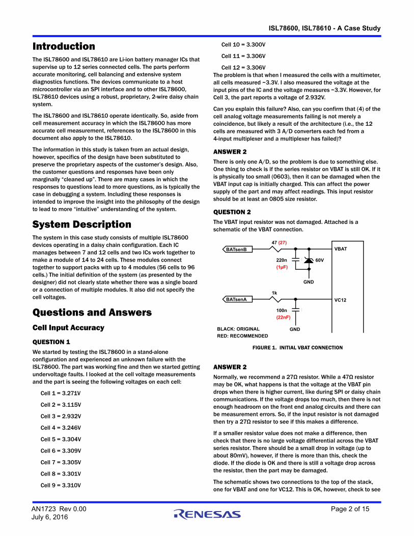
A: The fact that the upper device does not recognize the sleep/wake commands and there is no movement on the daisy
chain lines means that there is something wrong with the daisy chain. Nothing else matters until this can be cleared up.
What is the voltage on the DHI2 and DLO2 pins? DLO2 should be about 0.4V higher than DHI2 and both should be about VBAT(master)/2.
What is the voltage on the DHI1 and DLO1 pins? DLO1 should be about 0.4V higher than DHI1 and both should be about VBAT(top)/2.
What does the scope shot of the DHI2/DLO2 look like when sending the wake-up? It should look something like the signals in Figure 9.
Figure 9 shows the wake-up signals for multiple cascaded devices. Notice that before the device wakes up, the DHI2 and DLO2 signals are at about the same level. However, once awake, the DLO2 signal is slightly higher than the DHI2 signal.
Some other things to check:
Can you recheck to see that the C7/C9 common connection point ties to GND of the master and the C8/C10 common connection point ties to GND of the top device?
Did you check the voltage on the V3P3 pin? Is it solid when sending a command? If it dips, then there might not be enough voltage to get good communications.
What is the voltage on the V3P3 pin on the upper device? If it is about 2.9V, then the top device is still in sleep mode.
You might also need to make the EN pull-up resistor smaller than 1M (although it appears that the parts are enabled).
One other test you might try is to configure the board as a daisy chain, but send a stand-alone command. If you get a response, then there is a problem with the Comms select pin setup.
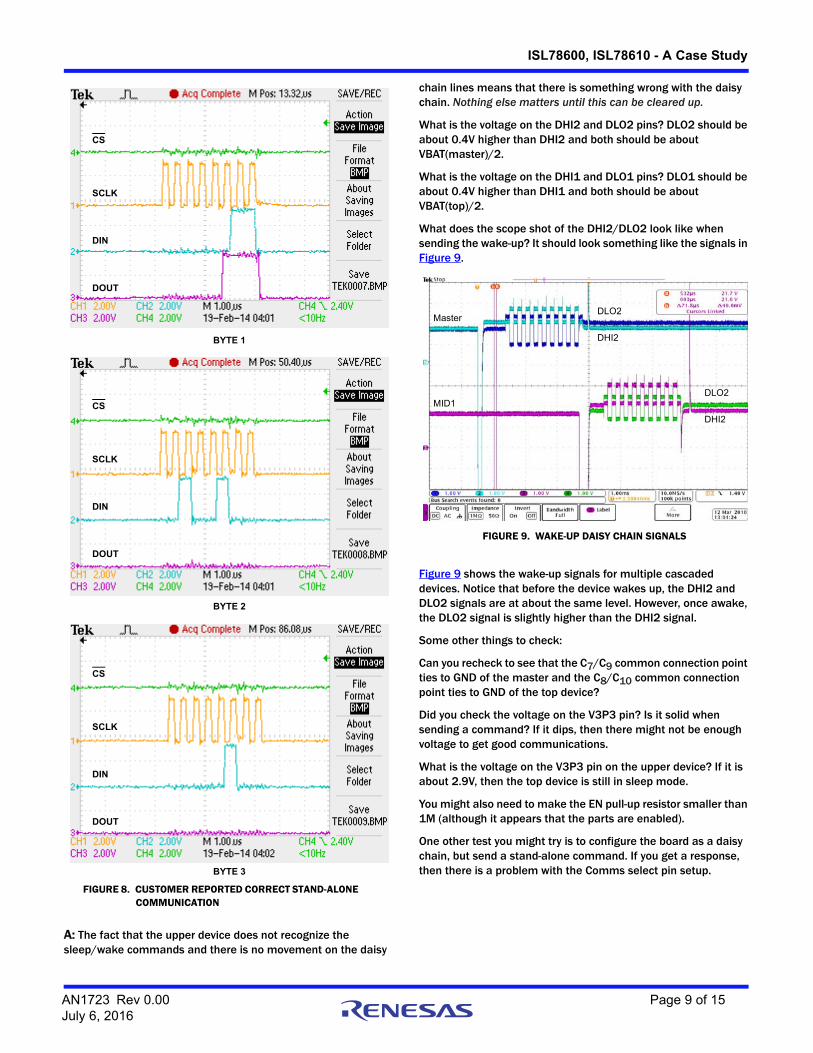
FIGURE 8. CUSTOMER REPORTED CORRECT STAND-ALONE COMMUNICATION
BYTE 1
BYTE 2
BYTE 3
CS
SCLK
DIN
DOUT
CS
SCLK
DIN
DOUT
CS
SCLK
DIN
DOUT
FIGURE 9. WAKE-UP DAISY CHAIN SIGNALS
DLO2
DHI2
Master
MID1DLO2
DHI2
AN1723 Rev 0.00 Page 9 of 15July 6, 2016
ISL78600, ISL78610 - A Case Study
Q: Before I connect the two boards through the two daisy chain wires I see the following conditions:
• For the master/bottom device:
- VBAT(bottom) = 23V relative to its BOT_GND
- Both DHI2 and DLO2 look like ~11.45V relative to BOT_GND
- The voltage measurement from DLO2 to DHI2 is ~263mV
• For the top device:
- VBAT(top) = 23V relative to TOP_GND
- Both DHI1 and DLO1 look like ~11.2V relative to TOP_GND
- The voltage measurement from DLO1 to DHI1 is ~265mV
So, that looks good. Figure 10 is the scope waveform for the master/bottom device's DHI2 and DLO2 lines, which actually look correct now while the daisy chain interface isn't connected. DLO2 is blue and DHI2 is orange.
I checked the common points. The C7/C9 common connection is connected to GND on the bottom board and the C8/C10 common connection is connected to GND on the top board.
The issue is that when I connected to the boards via the two daisy chain wires, the voltages on the master/bottom devices DHI2 and DLO2 go up to about ~22-23V.
A: The waveform in Figure 10 looks almost correct for daisy chain communications, however, it is still not what you want to see. When the boards properly connect, you should see that the waveforms are more symmetrical vertically; and before and after the signals there should be an offset between the two traces (while here they appear to be the same voltage).
Since the voltages appear good before connecting the daisy chain wires, It looks like there is an isolation problem. Perhaps DHI2 and DLO2 on the top device are being connected to the DHI2 and DLO2 of the bottom device when you connect the two boards with the daisy chain wires. If so, then this would absolutely be a bad thing.
Check to make sure the top and bottom boards are completely isolated. Nothing on the top board should touch the bottom board, except the VSS of the top tying to the BAT+ of the bottom and the communications through the capacitors. The DHI2/DLO2 on the top board should be floating.
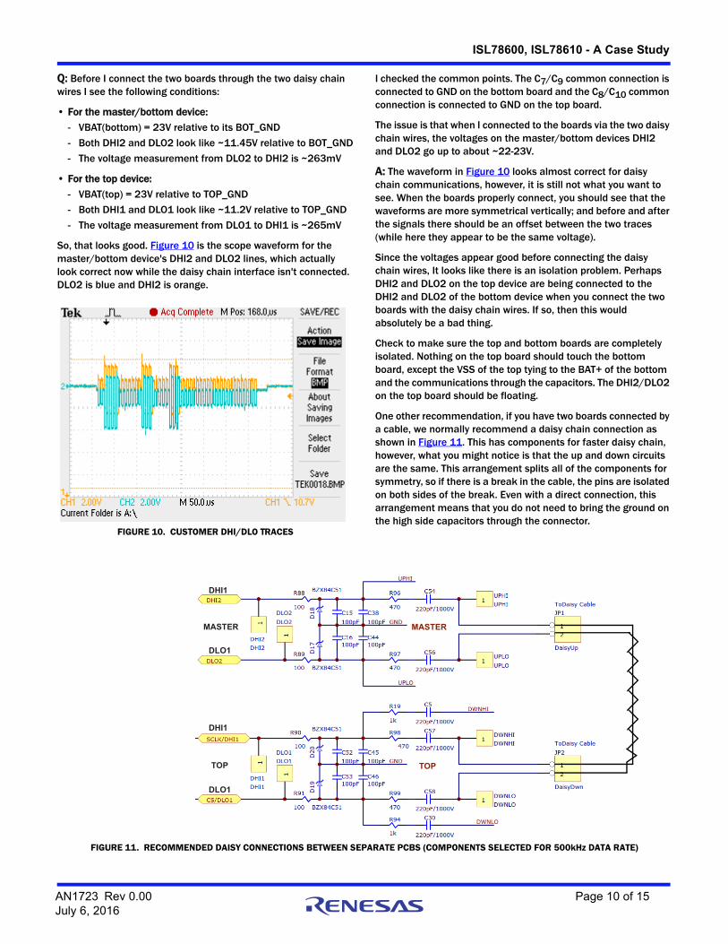
One other recommendation, if you have two boards connected by a cable, we normally recommend a daisy chain connection as shown in Figure 11. This has components for faster daisy chain, however, what you might notice is that the up and down circuits are the same. This arrangement splits all of the components for symmetry, so if there is a break in the cable, the pins are isolated on both sides of the break. Even with a direct connection, this arrangement means that you do not need to bring the ground on the high side capacitors through the connector.
FIGURE 10. CUSTOMER DHI/DLO TRACES
FIGURE 11. RECOMMENDED DAISY CONNECTIONS BETWEEN SEPARATE PCBS (COMPONENTS SELECTED FOR 500kHz DATA RATE)
DLO1
DHI1
MASTER
DLO1
DHI1
TOP TOP
MASTER
AN1723 Rev 0.00 Page 10 of 15July 6, 2016

ISL78600, ISL78610 - A Case Study
Q: Wow, it's been a long day. I think I finally got it right, however, I won't be able to check if valid data is coming back down the stack until tomorrow. Figure 12 are two waveforms showing my daisy chain communication. What I sent you last time was just the master/bottom side, since connecting them had the isolation issue I described. Once I fixed the isolation issue, I connected the 2-wire daisy chain interface and captured the attached waveforms.
A: This looks better.
Communication Software
QUESTION 12With the daisy chain HW issue resolved, I have been proceeding fairly successfully with the firmware development on our ISL78600 daisy chain cell balancing solution. I am starting with a 2 device stack and I can now bring the stack through the proper identify sequence. However, after the Identify sequence, I am getting NAKs in response to my attempts to program the limit registers (e.g., Overvoltage Limit).
The Identify TX/RX sequence looks like the following:
• TX = 0x032404
• RX = 0x0330000C
• TX = 0x032426
• RX = 0x03262000
• TX = 0x0327FE
• RX = 0x2330000B
Looking at these responses and according to the “Identify Section” of the datasheet, it looks like I am successful in the Identify process. Next I want to initialize my limit registers, for example, setting the Overvoltage Limit register (0b010000) to 0x17AE for a limit of ~3.7V. The issue is that when I send the write data command, I am getting a NAK response (see below)
• TX = 0x2A417AE6
• RX = 0x232C0001
The 0x2C in the response is a NAK that I would expect to be 0x30. Do you have any thoughts for why I am getting a NAK in response to this write data command?
ANSWER 12I set up two boards and sent a command to set the OV limit to 17AE and the GUI sent the following command.
TX = 0x2A417AE2
This has a “2” for the CRC, instead of “6” in your command. Perhaps that is the problem with communication.
I also get a response of:
0x2330000B
Please check your code for calculating the CRC. See Figure 5 on page 6 for our calculation routine.
QUESTION 13I have a few updates from the past week - in general, I believe I have made a number of improvements by modifying my communications code for the two device ISL78600 stack to be entirely interrupt and event driven, removing fixed delays in my code.
However, my initialization process is still giving me troubles. Once I get the stack to identify properly, I can communicate with the stack. The issue is that there are a number of times I don't get it to identify properly and there is the appearance of stack device #7 in a two device stack.
FIGURE 12. CUSTOMER DAISY WAVEFORMS AFTER CHANGES (GOOD)
ZOOM
AN1723 Rev 0.00 Page 11 of 15July 6, 2016

ISL78600, ISL78610 - A Case Study
I don't know how to programmatically account for all the wrong start-up states. The following is one set of incorrect commands and responses for an attempted Identify sequence -
• TX = 0x03 24 04
• RX = 0x00 30 00 0C (1-byte response)
• TX = 0x03 24 26
• RX = 0x03 26 20 00 (1-byte response)
• TX = 0x03 27 FE
• RX = 0x23 30 00 0B (1-byte response)
• TX = 0x13 30 0F
• RX = 0x23 2C 00 01
• RX = 0x13 30 00 06 (2-byte response)
The 'base id command' waveform (Figure 13) shows the transmission of 0x03 24 04 from the Host MCU to the bottom/master device, specifically, the timing between SPI bytes in the overall transmission of this command. The timing shows that this command meets the 100µs maximum requirement defined as the CS high time (the time between bytes). Please let me know if you see any concerns with the timing of my command transmission.
Also, the 'data_ready response handling' waveform (Figure 14), shows the timing on servicing the DATA_READY line. Please note that I have a level shifter that inverts DATA_READY from the ISL78600. As shown in the waveform, the DATA_READY signal goes HIGH when a byte is available in the ISL78600 buffer. The time that CS is low is the time it takes for me to read a SPI byte (~25µs). At the completion of each read with the rising edge of CS, you can see DATA_READY dip low briefly and return HIGH, indicating another byte is available. The time from the rising edge of DATA_READY to CS going low again is the time is takes for me to respond to the DATA_READY signal (~45-50µs). Do you think this is too long?
A final SPI question, when I transmit a command over SPI, like 0x03 24 04 on my 8-bit MCU, I send three separate bytes, with CS asserted separately for each byte like below. Is this incorrect of the application (i.e., should CS only be asserted once for the entire 3-byte command)?
CS = 0;
SPIWrite(0x03);
CS = 1;
CS = 0;
SPIWrite(0x24);
CS = 1;
CS = 0;
SPIWrite(0x04);
CS = 1;
FIGURE 13. CUSTOMER BASE ID COMMAND (SPI)
BLUE = SCKORANGE = MOSI
0x03 0x24 0x04
FIGURE 14. CUSTOMER DATA READY RESPONSE HANDLING TIMING
BLUE = CSORANGE = DATA_READY
AN1723 Rev 0.00 Page 12 of 15July 6, 2016
ISL78600, ISL78610 - A Case Study
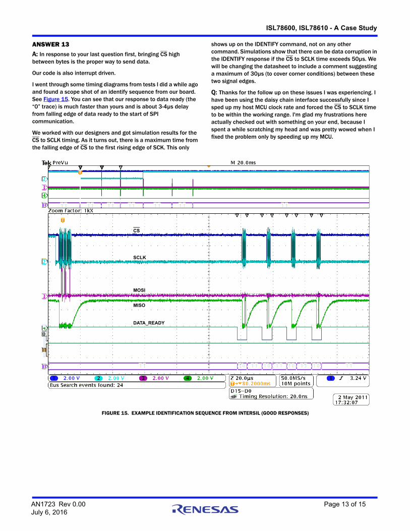
ANSWER 13A: In response to your last question first, bringing CS high between bytes is the proper way to send data.
Our code is also interrupt driven.
I went through some timing diagrams from tests I did a while ago and found a scope shot of an identify sequence from our board. See Figure 15. You can see that our response to data ready (the “0” trace) is much faster than yours and is about 3-4µs delay from falling edge of data ready to the start of SPI communication.
We worked with our designers and got simulation results for the CS to SCLK timing. As it turns out, there is a maximum time from the falling edge of CS to the first rising edge of SCK. This only
shows up on the IDENTIFY command, not on any other command. Simulations show that there can be data corruption in the IDENTIFY response if the CS to SCLK time exceeds 50µs. We will be changing the datasheet to include a comment suggesting a maximum of 30µs (to cover corner conditions) between these two signal edges.
Q: Thanks for the follow up on these issues I was experiencing. I have been using the daisy chain interface successfully since I sped up my host MCU clock rate and forced the CS to SCLK time to be within the working range. I'm glad my frustrations here actually checked out with something on your end, because I spent a while scratching my head and was pretty wowed when I fixed the problem only by speeding up my MCU.
FIGURE 15. EXAMPLE IDENTIFICATION SEQUENCE FROM INTERSIL (GOOD RESPONSES)
CS
SCLK
MOSI
MISO
DATA_READY
AN1723 Rev 0.00 Page 13 of 15July 6, 2016
ISL78600, ISL78610 - A Case Study
QUESTION 14In my application, I configured both boards for 7 cells (14 cells total for two ICs.) When I send a 'Scan All' command, the GUI notifies me that I have OW faults on both Device 1 and Device 2. Upon reading the OW Fault registers for Device 1 and Device 2, I find that the cells with faults are Cells 5 and 9.
ANSWER 14Did you set the bits in the CELL SETUP register? Set the bits that correspond to the unused inputs to “1”. This should exclude them from open wire, OV and UV faults.
QUESTION 15The SPI SCLK on the evaluation board appears to operate at 4MHz but the ISL78600 datasheet states 2MHz is the maximum. I am worried that something in my SPI or DATA_READY timing is too slow.
ANSWER 15The default SPI clock rate on the evaluation board is set to 4MHz. The datasheet lists 2MHz as the maximum clock speed, because 1MHz is all that is needed for to handle a 500kHz daisy chain frequency. However, the device can handle higher SCLK rates. If you want to try slower SPI clock rates using the GUI, you can set the SPI speed on the GUI. (Use the pull down menu at the top of the screen.)
PCB Layout
QUESTION 16I am in the process of laying out a new PCB. Do you have any guidelines?
ANSWER 16Please refer to reference designs and reference guidelines in ISL78600REFDESIGN and ISL78610REFDESIGN. These provide PCB layout recommendations as well as PCB design data bases. They can be ordered on memory stick under an NDA.
AN1723 Rev 0.00 Page 14 of 15July 6, 2016

http://www.renesas.comRefer to "http://www.renesas.com/" for the latest and detailed information.
Renesas Electronics America Inc.1001 Murphy Ranch Road, Milpitas, CA 95035, U.S.A.Tel: +1-408-432-8888, Fax: +1-408-434-5351Renesas Electronics Canada Limited9251 Yonge Street, Suite 8309 Richmond Hill, Ontario Canada L4C 9T3Tel: +1-905-237-2004Renesas Electronics Europe LimitedDukes Meadow, Millboard Road, Bourne End, Buckinghamshire, SL8 5FH, U.KTel: +44-1628-651-700, Fax: +44-1628-651-804Renesas Electronics Europe GmbHArcadiastrasse 10, 40472 Düsseldorf, Germany Tel: +49-211-6503-0, Fax: +49-211-6503-1327Renesas Electronics (China) Co., Ltd.Room 1709 Quantum Plaza, No.27 ZhichunLu, Haidian District, Beijing, 100191 P. R. ChinaTel: +86-10-8235-1155, Fax: +86-10-8235-7679Renesas Electronics (Shanghai) Co., Ltd.Unit 301, Tower A, Central Towers, 555 Langao Road, Putuo District, Shanghai, 200333 P. R. China Tel: +86-21-2226-0888, Fax: +86-21-2226-0999Renesas Electronics Hong Kong LimitedUnit 1601-1611, 16/F., Tower 2, Grand Century Place, 193 Prince Edward Road West, Mongkok, Kowloon, Hong KongTel: +852-2265-6688, Fax: +852 2886-9022Renesas Electronics Taiwan Co., Ltd.13F, No. 363, Fu Shing North Road, Taipei 10543, TaiwanTel: +886-2-8175-9600, Fax: +886 2-8175-9670Renesas Electronics Singapore Pte. Ltd.80 Bendemeer Road, Unit #06-02 Hyflux Innovation Centre, Singapore 339949Tel: +65-6213-0200, Fax: +65-6213-0300Renesas Electronics Malaysia Sdn.Bhd.Unit 1207, Block B, Menara Amcorp, Amcorp Trade Centre, No. 18, Jln Persiaran Barat, 46050 Petaling Jaya, Selangor Darul Ehsan, MalaysiaTel: +60-3-7955-9390, Fax: +60-3-7955-9510Renesas Electronics India Pvt. Ltd.No.777C, 100 Feet Road, HAL 2nd Stage, Indiranagar, Bangalore 560 038, IndiaTel: +91-80-67208700, Fax: +91-80-67208777Renesas Electronics Korea Co., Ltd.17F, KAMCO Yangjae Tower, 262, Gangnam-daero, Gangnam-gu, Seoul, 06265 KoreaTel: +82-2-558-3737, Fax: +82-2-558-5338
SALES OFFICES
© 2018 Renesas Electronics Corporation. All rights reserved.Colophon 7.0
(Rev.4.0-1 November 2017)
Notice
1. Descriptions of circuits, software and other related information in this document are provided only to illustrate the operation of semiconductor products and application examples. You are fully responsible for
the incorporation or any other use of the circuits, software, and information in the design of your product or system. Renesas Electronics disclaims any and all liability for any losses and damages incurred by
you or third parties arising from the use of these circuits, software, or information.
2. Renesas Electronics hereby expressly disclaims any warranties against and liability for infringement or any other claims involving patents, copyrights, or other intellectual property rights of third parties, by or
arising from the use of Renesas Electronics products or technical information described in this document, including but not limited to, the product data, drawings, charts, programs, algorithms, and application
examples.
3. No license, express, implied or otherwise, is granted hereby under any patents, copyrights or other intellectual property rights of Renesas Electronics or others.
4. You shall not alter, modify, copy, or reverse engineer any Renesas Electronics product, whether in whole or in part. Renesas Electronics disclaims any and all liability for any losses or damages incurred by
you or third parties arising from such alteration, modification, copying or reverse engineering.
5. Renesas Electronics products are classified according to the following two quality grades: “Standard” and “High Quality”. The intended applications for each Renesas Electronics product depends on the
product’s quality grade, as indicated below.
"Standard": Computers; office equipment; communications equipment; test and measurement equipment; audio and visual equipment; home electronic appliances; machine tools; personal electronic
equipment; industrial robots; etc.
"High Quality": Transportation equipment (automobiles, trains, ships, etc.); traffic control (traffic lights); large-scale communication equipment; key financial terminal systems; safety control equipment; etc.
Unless expressly designated as a high reliability product or a product for harsh environments in a Renesas Electronics data sheet or other Renesas Electronics document, Renesas Electronics products are
not intended or authorized for use in products or systems that may pose a direct threat to human life or bodily injury (artificial life support devices or systems; surgical implantations; etc.), or may cause
serious property damage (space system; undersea repeaters; nuclear power control systems; aircraft control systems; key plant systems; military equipment; etc.). Renesas Electronics disclaims any and all
liability for any damages or losses incurred by you or any third parties arising from the use of any Renesas Electronics product that is inconsistent with any Renesas Electronics data sheet, user’s manual or
other Renesas Electronics document.
6. When using Renesas Electronics products, refer to the latest product information (data sheets, user’s manuals, application notes, “General Notes for Handling and Using Semiconductor Devices” in the
reliability handbook, etc.), and ensure that usage conditions are within the ranges specified by Renesas Electronics with respect to maximum ratings, operating power supply voltage range, heat dissipation
characteristics, installation, etc. Renesas Electronics disclaims any and all liability for any malfunctions, failure or accident arising out of the use of Renesas Electronics products outside of such specified
ranges.
7. Although Renesas Electronics endeavors to improve the quality and reliability of Renesas Electronics products, semiconductor products have specific characteristics, such as the occurrence of failure at a
certain rate and malfunctions under certain use conditions. Unless designated as a high reliability product or a product for harsh environments in a Renesas Electronics data sheet or other Renesas
Electronics document, Renesas Electronics products are not subject to radiation resistance design. You are responsible for implementing safety measures to guard against the possibility of bodily injury, injury
or damage caused by fire, and/or danger to the public in the event of a failure or malfunction of Renesas Electronics products, such as safety design for hardware and software, including but not limited to
redundancy, fire control and malfunction prevention, appropriate treatment for aging degradation or any other appropriate measures. Because the evaluation of microcomputer software alone is very difficult
and impractical, you are responsible for evaluating the safety of the final products or systems manufactured by you.
8. Please contact a Renesas Electronics sales office for details as to environmental matters such as the environmental compatibility of each Renesas Electronics product. You are responsible for carefully and
sufficiently investigating applicable laws and regulations that regulate the inclusion or use of controlled substances, including without limitation, the EU RoHS Directive, and using Renesas Electronics
products in compliance with all these applicable laws and regulations. Renesas Electronics disclaims any and all liability for damages or losses occurring as a result of your noncompliance with applicable
laws and regulations.
9. Renesas Electronics products and technologies shall not be used for or incorporated into any products or systems whose manufacture, use, or sale is prohibited under any applicable domestic or foreign laws
or regulations. You shall comply with any applicable export control laws and regulations promulgated and administered by the governments of any countries asserting jurisdiction over the parties or
transactions.
10. It is the responsibility of the buyer or distributor of Renesas Electronics products, or any other party who distributes, disposes of, or otherwise sells or transfers the product to a third party, to notify such third
party in advance of the contents and conditions set forth in this document.
11. This document shall not be reprinted, reproduced or duplicated in any form, in whole or in part, without prior written consent of Renesas Electronics.
12. Please contact a Renesas Electronics sales office if you have any questions regarding the information contained in this document or Renesas Electronics products.
(Note 1) “Renesas Electronics” as used in this document means Renesas Electronics Corporation and also includes its directly or indirectly controlled subsidiaries.
(Note 2) “Renesas Electronics product(s)” means any product developed or manufactured by or for Renesas Electronics.