Embed Size (px)
Citation preview
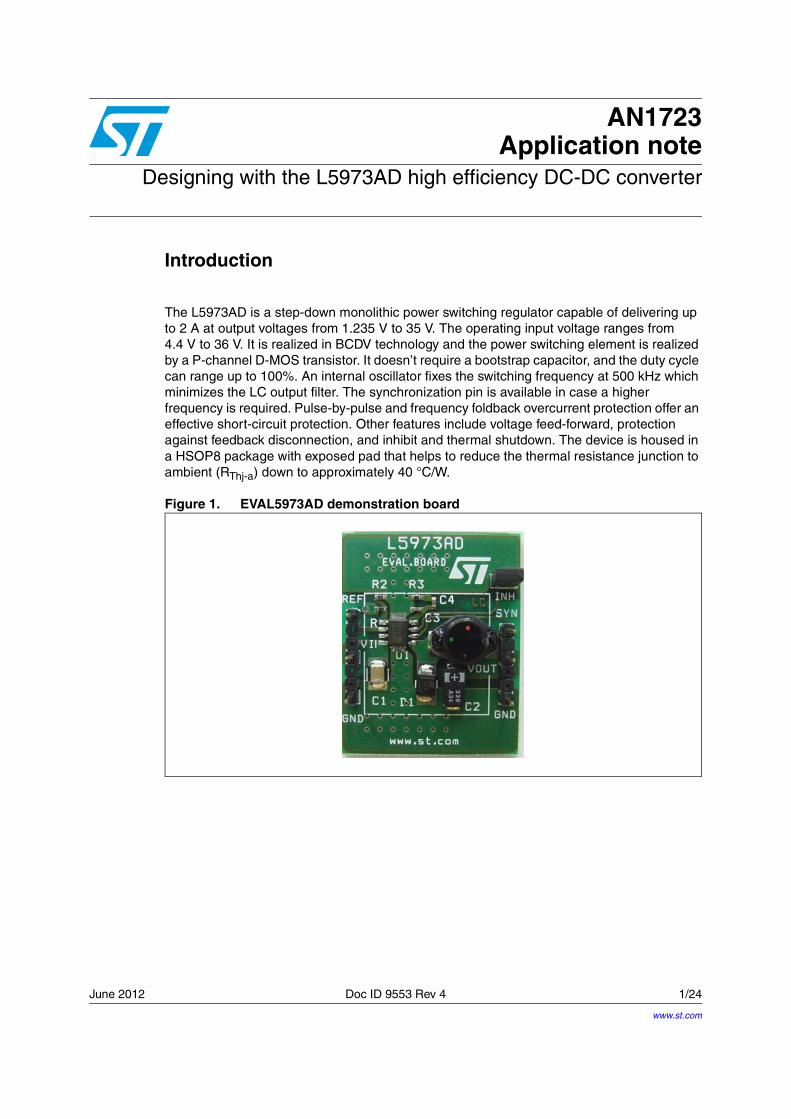
June 2012 Doc ID 9553 Rev 4 1/24
AN1723Application note
Designing with the L5973AD high efficiency DC-DC converter
Introduction
The L5973AD is a step-down monolithic power switching regulator capable of delivering up to 2 A at output voltages from 1.235 V to 35 V. The operating input voltage ranges from 4.4 V to 36 V. It is realized in BCDV technology and the power switching element is realized by a P-channel D-MOS transistor. It doesn’t require a bootstrap capacitor, and the duty cycle can range up to 100%. An internal oscillator fixes the switching frequency at 500 kHz which minimizes the LC output filter. The synchronization pin is available in case a higher frequency is required. Pulse-by-pulse and frequency foldback overcurrent protection offer an effective short-circuit protection. Other features include voltage feed-forward, protection against feedback disconnection, and inhibit and thermal shutdown. The device is housed in a HSOP8 package with exposed pad that helps to reduce the thermal resistance junction to ambient (RThj-a) down to approximately 40 °C/W.
Figure 1. EVAL5973AD demonstration board
www.st.com
Contents AN1723
2/24 Doc ID 9553 Rev 4
Contents
1 Pin description . . . . . . . . . . . . . . . . . . . . . . . . . . . . . . . . . . . . . . . . . . . . . 4
2 Application information . . . . . . . . . . . . . . . . . . . . . . . . . . . . . . . . . . . . . . 5
3 Component selection . . . . . . . . . . . . . . . . . . . . . . . . . . . . . . . . . . . . . . . . 8
3.1 Input capacitor . . . . . . . . . . . . . . . . . . . . . . . . . . . . . . . . . . . . . . . . . . . . . . 8
4 Output capacitor . . . . . . . . . . . . . . . . . . . . . . . . . . . . . . . . . . . . . . . . . . . . 9
4.1 Inductor . . . . . . . . . . . . . . . . . . . . . . . . . . . . . . . . . . . . . . . . . . . . . . . . . . . 9
5 Closing the loop . . . . . . . . . . . . . . . . . . . . . . . . . . . . . . . . . . . . . . . . . . . 11
5.1 Error amplifier and compensation network . . . . . . . . . . . . . . . . . . . . . . . . 11
5.2 LC filter . . . . . . . . . . . . . . . . . . . . . . . . . . . . . . . . . . . . . . . . . . . . . . . . . . . 12
5.3 PWM comparator . . . . . . . . . . . . . . . . . . . . . . . . . . . . . . . . . . . . . . . . . . . 13
6 Layout considerations . . . . . . . . . . . . . . . . . . . . . . . . . . . . . . . . . . . . . . 15
6.1 Thermal considerations . . . . . . . . . . . . . . . . . . . . . . . . . . . . . . . . . . . . . . 16
6.2 Short-circuit protection . . . . . . . . . . . . . . . . . . . . . . . . . . . . . . . . . . . . . . . 17
7 Application ideas . . . . . . . . . . . . . . . . . . . . . . . . . . . . . . . . . . . . . . . . . . . 19
7.1 Positive buck-boost regulator . . . . . . . . . . . . . . . . . . . . . . . . . . . . . . . . . . 19
7.2 Buck-boost regulator . . . . . . . . . . . . . . . . . . . . . . . . . . . . . . . . . . . . . . . . 19
7.3 Dual output voltage with auxiliary winding . . . . . . . . . . . . . . . . . . . . . . . . 20
7.4 Synchronization example . . . . . . . . . . . . . . . . . . . . . . . . . . . . . . . . . . . . . 20
7.5 Compensation network with MLCC (multiple layer ceramic capacitor)
at the output . . . . . . . . . . . . . . . . . . . . . . . . . . . . . . . . . . . . . . . . . . . . . . . 21
7.6 External soft-start network . . . . . . . . . . . . . . . . . . . . . . . . . . . . . . . . . . . . 22
8 Revision history . . . . . . . . . . . . . . . . . . . . . . . . . . . . . . . . . . . . . . . . . . . 23
AN1723 List of figures
Doc ID 9553 Rev 4 3/24
List of figures
Figure 1. EVAL5973AD demonstration board . . . . . . . . . . . . . . . . . . . . . . . . . . . . . . . . . . . . . . . . . . . 1Figure 2. Package . . . . . . . . . . . . . . . . . . . . . . . . . . . . . . . . . . . . . . . . . . . . . . . . . . . . . . . . . . . . . . . . 4Figure 3. Pin connection . . . . . . . . . . . . . . . . . . . . . . . . . . . . . . . . . . . . . . . . . . . . . . . . . . . . . . . . . . . 4Figure 4. Demonstration board application circuit . . . . . . . . . . . . . . . . . . . . . . . . . . . . . . . . . . . . . . . . 5Figure 5. PCB layout (component side) . . . . . . . . . . . . . . . . . . . . . . . . . . . . . . . . . . . . . . . . . . . . . . . . 6Figure 6. PCB layout (bottom side) . . . . . . . . . . . . . . . . . . . . . . . . . . . . . . . . . . . . . . . . . . . . . . . . . . . 6Figure 7. PCB layout (front side) . . . . . . . . . . . . . . . . . . . . . . . . . . . . . . . . . . . . . . . . . . . . . . . . . . . . . 6Figure 8. Junction temperature vs. output current at VIN = 5 V. . . . . . . . . . . . . . . . . . . . . . . . . . . . . . 7Figure 9. Junction temperature vs. output current at VIN = 12 V. . . . . . . . . . . . . . . . . . . . . . . . . . . . . 7Figure 10. Efficiency vs. output current at VIN = 5 V . . . . . . . . . . . . . . . . . . . . . . . . . . . . . . . . . . . . . . . 7Figure 11. Efficiency vs. output current at VIN = 12 V . . . . . . . . . . . . . . . . . . . . . . . . . . . . . . . . . . . . . . 7Figure 12. Block diagram . . . . . . . . . . . . . . . . . . . . . . . . . . . . . . . . . . . . . . . . . . . . . . . . . . . . . . . . . . . 11Figure 13. Error amplifier equivalent circuit and compensation network . . . . . . . . . . . . . . . . . . . . . . . 12Figure 14. Module plot . . . . . . . . . . . . . . . . . . . . . . . . . . . . . . . . . . . . . . . . . . . . . . . . . . . . . . . . . . . . . 14Figure 15. Phase plot. . . . . . . . . . . . . . . . . . . . . . . . . . . . . . . . . . . . . . . . . . . . . . . . . . . . . . . . . . . . . . 15Figure 16. Layout example . . . . . . . . . . . . . . . . . . . . . . . . . . . . . . . . . . . . . . . . . . . . . . . . . . . . . . . . . 16Figure 17. Short-circuit current VIN = 25 V . . . . . . . . . . . . . . . . . . . . . . . . . . . . . . . . . . . . . . . . . . . . . 18Figure 18. Short-circuit current VIN = 30 V . . . . . . . . . . . . . . . . . . . . . . . . . . . . . . . . . . . . . . . . . . . . . 18Figure 19. Positive buck-boost regulator . . . . . . . . . . . . . . . . . . . . . . . . . . . . . . . . . . . . . . . . . . . . . . . 19Figure 20. Buck-boost regulator. . . . . . . . . . . . . . . . . . . . . . . . . . . . . . . . . . . . . . . . . . . . . . . . . . . . . . 20Figure 21. Dual output voltage with auxiliary winding . . . . . . . . . . . . . . . . . . . . . . . . . . . . . . . . . . . . . 20Figure 22. Synchronization example . . . . . . . . . . . . . . . . . . . . . . . . . . . . . . . . . . . . . . . . . . . . . . . . . . 21Figure 23. MLCC compensation network example . . . . . . . . . . . . . . . . . . . . . . . . . . . . . . . . . . . . . . . 21Figure 24. Soft-start network example . . . . . . . . . . . . . . . . . . . . . . . . . . . . . . . . . . . . . . . . . . . . . . . . . 22
Pin description AN1723
4/24 Doc ID 9553 Rev 4
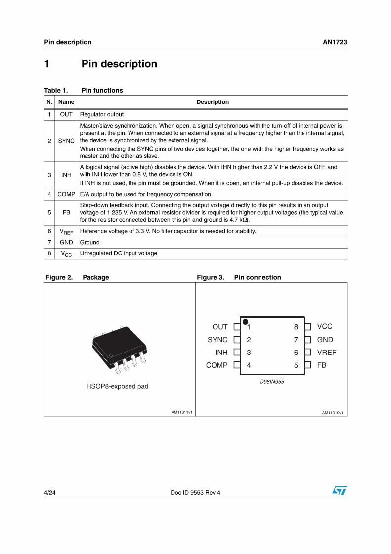
1 Pin description
Table 1. Pin functions
N. Name Description
1 OUT Regulator output
2 SYNC
Master/slave synchronization. When open, a signal synchronous with the turn-off of internal power is present at the pin. When connected to an external signal at a frequency higher than the internal signal, the device is synchronized by the external signal.When connecting the SYNC pins of two devices together, the one with the higher frequency works as master and the other as slave.
3 INHA logical signal (active high) disables the device. With IHN higher than 2.2 V the device is OFF and with INH lower than 0.8 V, the device is ON.
If INH is not used, the pin must be grounded. When it is open, an internal pull-up disables the device.
4 COMP E/A output to be used for frequency compensation.
5 FBStep-down feedback input. Connecting the output voltage directly to this pin results in an output voltage of 1.235 V. An external resistor divider is required for higher output voltages (the typical value for the resistor connected between this pin and ground is 4.7 kΩ).
6 VREF Reference voltage of 3.3 V. No filter capacitor is needed for stability.
7 GND Ground
8 VCC Unregulated DC input voltage.
Figure 2. Package Figure 3. Pin connection
AM11311v1
HSOP8-exposed pad
OUT
SYNC
INH
COMP
1
3
2
4
VCC
VREF
GND
FB
8
7
6
5
D98IN955
AM11310v1
AN1723 Application information
Doc ID 9553 Rev 4 5/24
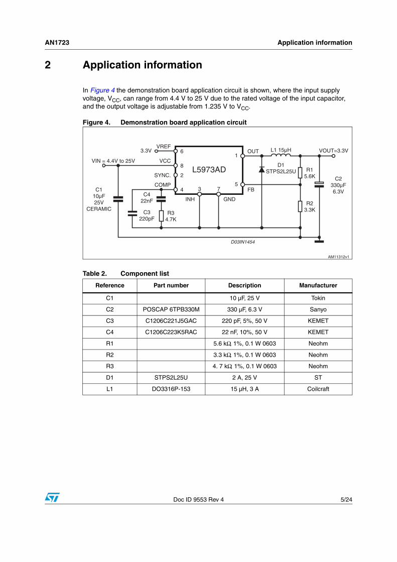
2 Application information
In Figure 4 the demonstration board application circuit is shown, where the input supply voltage, VCC, can range from 4.4 V to 25 V due to the rated voltage of the input capacitor, and the output voltage is adjustable from 1.235 V to VCC.
Figure 4. Demonstration board application circuit
Table 2. Component list
Reference Part number Description Manufacturer
C1 10 µF, 25 V Tokin
C2 POSCAP 6TPB330M 330 µF, 6.3 V Sanyo
C3 C1206C221J5GAC 220 pF, 5%, 50 V KEMET
C4 C1206C223K5RAC 22 nF, 10%, 50 V KEMET
R1 5.6 kΩ, 1%, 0.1 W 0603 Neohm
R2 3.3 kΩ, 1%, 0.1 W 0603 Neohm
R3 4. 7 kΩ, 1%, 0.1 W 0603 Neohm
D1 STPS2L25U 2 A, 25 V ST
L1 DO3316P-153 15 µH, 3 A Coilcraft
D03IN1454
8
45
1
7
L5973AD
C110µF25V
CERAMIC
C2330µF6.3V
VOUT=3.3V
VIN = 4.4V to 25V
R15.6K
R23.3K
R34.7K
C422nF
C3220pF
3
L1 15µH
D1STPS2L25U
COMP
VCC
OUT
FB
GNDINH
2
63.3V
SYNC.
VREF
AM11312v1
Application information AN1723
6/24 Doc ID 9553 Rev 4
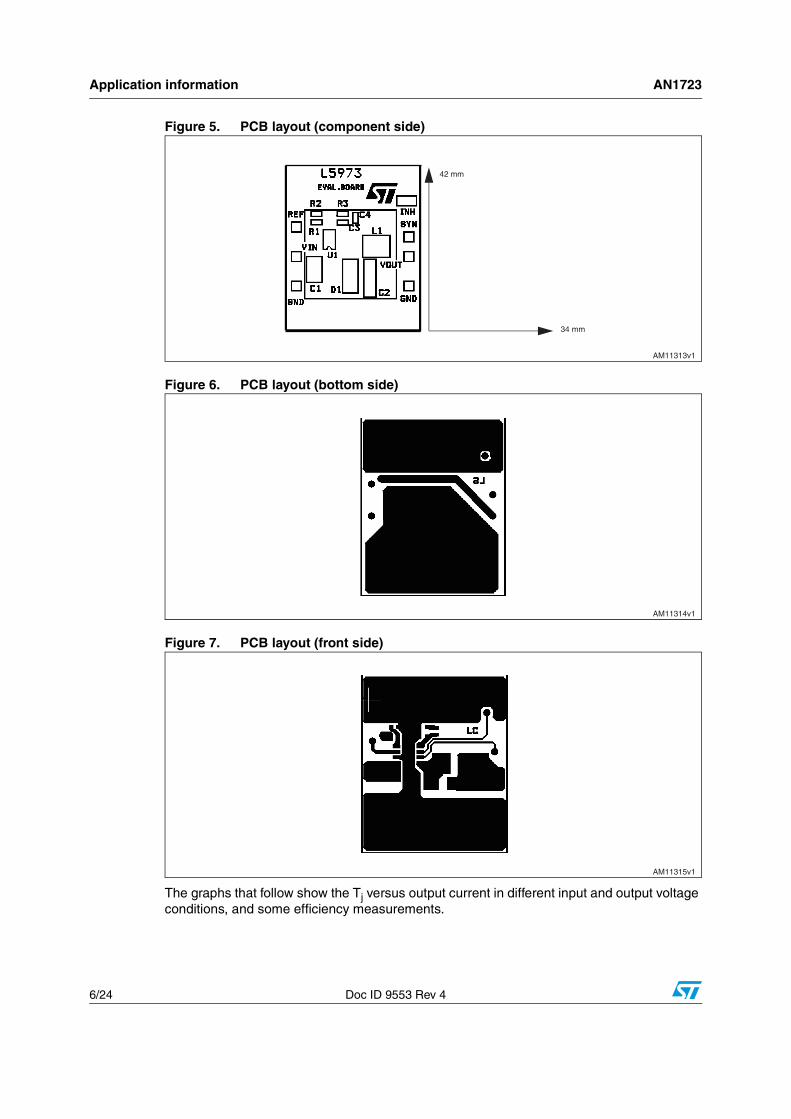
Figure 5. PCB layout (component side)
Figure 6. PCB layout (bottom side)
Figure 7. PCB layout (front side)
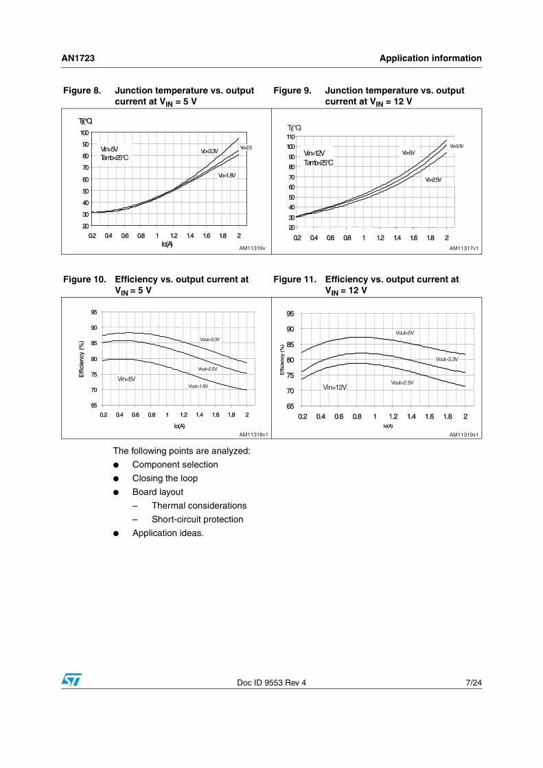
The graphs that follow show the Tj versus output current in different input and output voltage conditions, and some efficiency measurements.
AM11313v1
42 mm
34 mm
AM11314v1
F
AM11315v1
AN1723 Application information
Doc ID 9553 Rev 4 7/24
The following points are analyzed:
● Component selection
● Closing the loop
● Board layout
– Thermal considerations
– Short-circuit protection
● Application ideas.
Figure 8. Junction temperature vs. output current at VIN = 5 V
Figure 9. Junction temperature vs. output current at VIN = 12 V
20
30
40
50
60
70
80
90
100
0.2 0.4 0.6 0.8 1 1.2 1.4 1.6 1.8 2Io(A)
Tj(°C)
Vo=2.5Vo=3.3V
Vo=1.8V
Vin=5VTamb=25°C
20
30
40
50
60
70
80
90
100
0.2 0.4 0.6 0.8 1 1.2 1.4 1.6 1.8 2Io(A)
Tj(°C)
Vo=2.5Vo=3.3V
Vo=1.8V
Vin=5VTamb=25°C
AM11316v AM11317v1
Tj( C)
20
30
40
50
60
70
80
90
100
110
0.2 0.4 0.6 0.8 1 1.2 1.4 1.6 1.8 2
Vin=12VTamb=25°C
Vo=3.3V
Vo=5V
Vo=2.5V
20
30
40
50
60
70
80
90
100
110
0.2 0.4 0.6 0.8 1 1.2 1.4 1.6 1.8 2
Vin=12VTamb=25°C
Vo=3.3V
Vo=5V
Vo=2.5V
Tj(°C)
Figure 10. Efficiency vs. output current at VIN = 5 V
Figure 11. Efficiency vs. output current at VIN = 12 V
AM11318v1
65
70
75
80
85
90
95
0.2 0.4 0.6 0.8 1 1.2 1.4 1.6 1.8 2
Io(A)
Effi
cien
cy (
%)
Vin=5V
Vout=2.5V
Vout=3.3V
Vout=1.8V
65
70
75
80
85
90
95
0.2 0.4 0.6 0.8 1 1.2 1.4 1.6 1.8 2
Io(A)
Effi
cien
cy (
%)
Vin=5V
Vout=2.5V
Vout=3.3V
Vout=1.8V
AM11319v1
65
70
75
80
85
90
95
0.2 0.4 0.6 0.8 1 1.2 1.4 1.6 1.8 2Io(A)
Effi
cien
cy (
%)
Vin=12V
Vout=3.3V
Vout=2.5V
Vout=5V
65
70
75
80
85
90
95
0.2 0.4 0.6 0.8 1 1.2 1.4 1.6 1.8 2Io(A)
Effi
cien
cy (
%)
Vin=12V
Vout=3.3V
Vout=2.5V
Vout=5V
Component selection AN1723
8/24 Doc ID 9553 Rev 4
3 Component selection
3.1 Input capacitorThe input capacitor must be able to support the maximum input operating voltage and the maximum RMS input current.
Since step-down converters draw current from the input in pulses, the input current is squared and the height of each pulse is equal to the output current. The input capacitor must absorb all this switching current which can be up to the load current divided by two (worst case, with duty cycle of 50%). For this reason, the quality of these capacitors must be very high to minimize the power dissipation generated by the internal ESR, thereby improving system reliability and efficiency.
The critical parameter is usually the RMS current rating, which must be higher than the RMS input current. The maximum RMS input current (flowing through the input capacitor) is:
Equation 1
where η is the expected system efficiency, D is the duty cycle and IO the output DC current. This function reaches its maximum value at D = 0.5 and the equivalent RMS current is equal to IO divided by 2 (considering η = 1).
The maximum and minimum duty cycles are:
Equation 2
Equation 3
where VF is the freewheeling diode forward voltage and VSW the voltage drop across the internal PDMOS. Considering the range DMIN to DMAX it is possible to determine the max. IRMS flowing through the input capacitor. Different capacitors can be considered:
● Electrolytic capacitors
These are the most commonly used due to their low cost and wide range of RMS current ratings. The only drawback is that, considering ripple current rating requirements, they are physically larger than other capacitors.
● Ceramic capacitors
If available for the required value and voltage rating, these capacitors usually have a higher RMS current rating for a given physical dimension (due to the very low ESR). The drawback is their high cost.
● Tantalum capacitor
Small, good quality tantalum capacitors with very low ESR are becoming more available. However, they can occasionally burn if subjected to very high current during charge. Therefore, it is better to avoid this type of capacitor for the input filter of the device. They can, however, be subjected to high surge current when connected to the power supply.
IRMS IO D 2 D2⋅
η------------------– D
2
η-------+⋅=
IRMS IO D 2 D2⋅
η------------------– D
2
η-------+⋅=
DMAX
VOUT VF+
VINMIN VSW–------------------------------------------ and D
VOUT VF+
VINMAX VSW–--------------------------------------------= =
AN1723 Output capacitor
Doc ID 9553 Rev 4 9/24
4 Output capacitor
The output capacitor is very important in order to satisfy the output voltage ripple requirement. Using a small inductor value is useful to reduce the size of the choke but increases the current ripple. So, to reduce the output voltage ripple, a low ESR capacitor is required. Nevertheless, the ESR of the output capacitor introduces a zero in the open loop gain, which helps to increase the phase margin of the system. If the zero goes to every high frequency, its effect is negligible. For this reason, ceramic capacitors and very low ESR capacitors in general should be avoided. Tantalum and electrolytic capacitors are usually a good choice for this purpose. A list of some tantalum capacitor manufacturers is provided in Table 3.
4.1 InductorThe inductor value is very important as it fixes the ripple current flowing through the output capacitor. The ripple current is usually fixed at 20-40% of IOmax, which is 0.3-0.6 A with IOmax = 1.5 A. The approximate inductor value is obtained using the following formula:
Equation 4
where TON is the ON time of the internal switch, given by D · T. For example, with VOUT = 3.3 V, VIN = 12 V and ΔIO = 0.45 A, the minimum inductor value is about 12 µH.
The peak current through the inductor is given by:
Equation 5
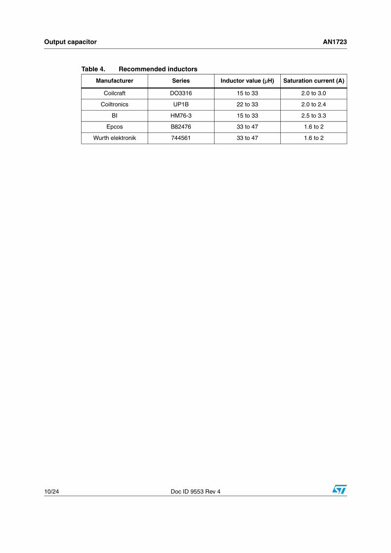
and it can be observed that if the inductor value decreases, the peak current (which must be lower than the current limit of the device) increases. So, when the peak current is fixed, a higher inductor value allows a higher value for the output current. In Table 4, some inductor manufacturers are listed.
Table 3. Recommended output capacitors
Manufacturer Series Cap value (μF) Rated voltage (V) ESR (mΩ)
AVX TPS 100 to 470 4 to 35 50 to 200
KEMET T494/5 100 to 470 4 to 20 30 to 200
Sanyo POSCAP (1) TPA/B/C 100 to 470 4 to 16 40 to 80
Sprague 595D 220 to 390 4 to 20 160 to 650
1. POSCAP capacitors have characteristics very similar to tantalum capacitors.
LVIN VOUT–( )
IΔ--------------------------------------- TON⋅=
IPK IOIΔ
2-----+=
Output capacitor AN1723
10/24 Doc ID 9553 Rev 4
Table 4. Recommended inductors
Manufacturer Series Inductor value (µH) Saturation current (A)
Coilcraft DO3316 15 to 33 2.0 to 3.0
Coiltronics UP1B 22 to 33 2.0 to 2.4
BI HM76-3 15 to 33 2.5 to 3.3
Epcos B82476 33 to 47 1.6 to 2
Wurth elektronik 744561 33 to 47 1.6 to 2
AN1723 Closing the loop
Doc ID 9553 Rev 4 11/24
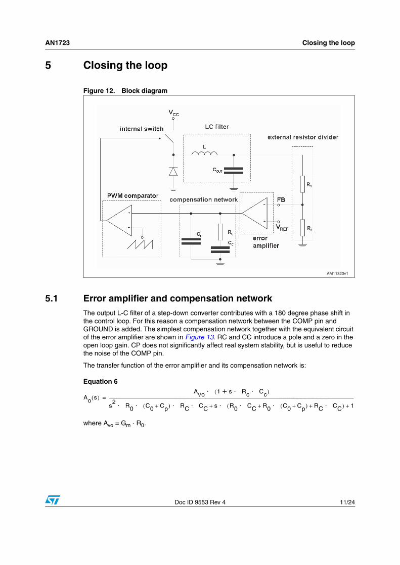
5 Closing the loop
Figure 12. Block diagram
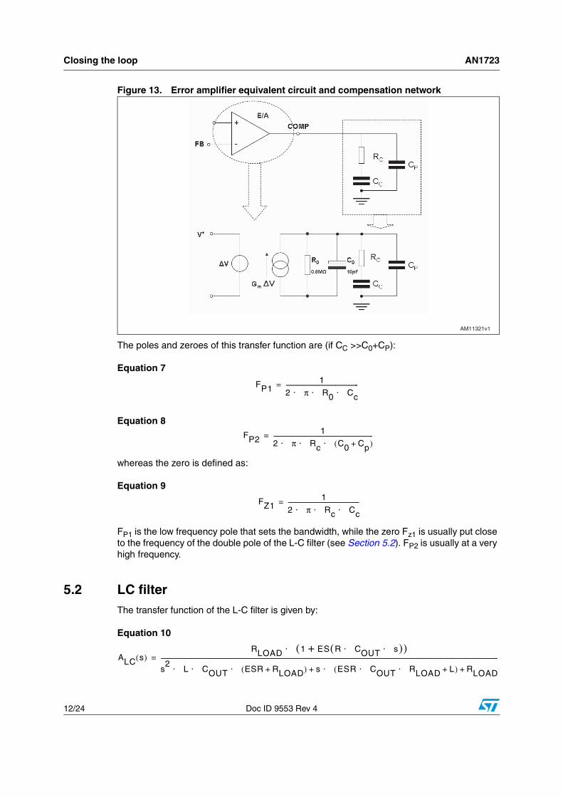
5.1 Error amplifier and compensation networkThe output L-C filter of a step-down converter contributes with a 180 degree phase shift in the control loop. For this reason a compensation network between the COMP pin and GROUND is added. The simplest compensation network together with the equivalent circuit of the error amplifier are shown in Figure 13. RC and CC introduce a pole and a zero in the open loop gain. CP does not significantly affect real system stability, but is useful to reduce the noise of the COMP pin.
The transfer function of the error amplifier and its compensation network is:
Equation 6
where Avo = Gm · R0.
AM11320v1
Ao s( )Avo 1 s Rc Cc⋅ ⋅+( )⋅
s2
R0 C0 Cp+( ) RC CC s R0 CC R0 C0 Cp+( ) RC CC⋅+⋅+⋅( ) 1+⋅+⋅ ⋅ ⋅ ⋅---------------------------------------------------------------------------------------------------------------------------------------------------------------------------------------------------------------------------------------------------=
Closing the loop AN1723
12/24 Doc ID 9553 Rev 4
Figure 13. Error amplifier equivalent circuit and compensation network
The poles and zeroes of this transfer function are (if CC >>C0+CP):
Equation 7
Equation 8
whereas the zero is defined as:
Equation 9
FP1 is the low frequency pole that sets the bandwidth, while the zero Fz1 is usually put close to the frequency of the double pole of the L-C filter (see Section 5.2). FP2 is usually at a very high frequency.
5.2 LC filterThe transfer function of the L-C filter is given by:
Equation 10
AM11321v1
FP11
2 π R0 Cc⋅ ⋅ ⋅---------------------------------------------------=
FP21
2 π Rc C0 Cp+( )⋅ ⋅ ⋅----------------------------------------------------------------------=
FZ11
2 π Rc Cc⋅ ⋅ ⋅--------------------------------------------------=
ALC s( )RLOAD 1 ES R COUT s⋅ ⋅( )+( )⋅
s2
L COUT ESR RLOAD+( ) s ESR COUT RLOAD L+⋅ ⋅( ) RLOAD+⋅+⋅ ⋅ ⋅----------------------------------------------------------------------------------------------------------------------------------------------------------------------------------------------------------------------------------------------=
AN1723 Closing the loop
Doc ID 9553 Rev 4 13/24
where RLOAD is defined as the ratio between VOUT and IOUT.
If RLOAD>>ESR, the previous expression of ALC can be simplified and becomes:
Equation 11
The zero of this transfer function is given by:
Equation 12
F0 is the zero introduced by the ESR of the output capacitor and is very important to increase the phase margin of the loop.
The poles of the transfer function can be calculated through the following expression:
Equation 13
In the denominator of ALC, the typical second order system equation can be recognized:
Equation 14
If the damping coefficient δ is very close to zero, the roots of the equation become a double root whose value is ωn.
Similarly for ALC, the poles can usually be defined as a double pole whose value is:
Equation 15
5.3 PWM comparatorThe PWM gain is given by the following formula:
Equation 16
where VOSCMAX is the maximum value of a sawtooth waveform, and VOSCMIN is the minimum value. A voltage feed-forward is implemented to ensure a constant GPWM. This is obtained generating a sawtooth waveform directly proportional to the input voltage VCC.
ALC s( )1 ESR COUT s⋅ ⋅+
L COUT s2
ESR COUT s 1+⋅ ⋅+⋅ ⋅---------------------------------------------------------------------------------------------------------------------=
F01
2 π ESR COUT⋅ ⋅ ⋅------------------------------------------------------------------=
FPLC1 2,ESR COUT ESR COUT⋅( )2
4 L COUT⋅ ⋅( )–±⋅( )–
2 L COUT⋅ ⋅-----------------------------------------------------------------------------------------------------------------------------------------------------------------------=
s2
2 δ ωn s ω2n+⋅ ⋅ ⋅+
FPLC1
2 π L COUT⋅⋅ ⋅----------------------------------------------------------=
GPWM s( )VCC
VOSCMAX VOSCMIN–( )------------------------------------------------------------------------=
Closing the loop AN1723
14/24 Doc ID 9553 Rev 4
Equation 17
where K is equal to 0.152. Therefore the PWM gain is also equal to:
Equation 18
This means that even if the input voltage changes, the error amplifier does not change its value to keep the loop in regulation, therefore ensuring better line regulation and line transient response. In summary, the open loop gain can be written as:
Equation 19
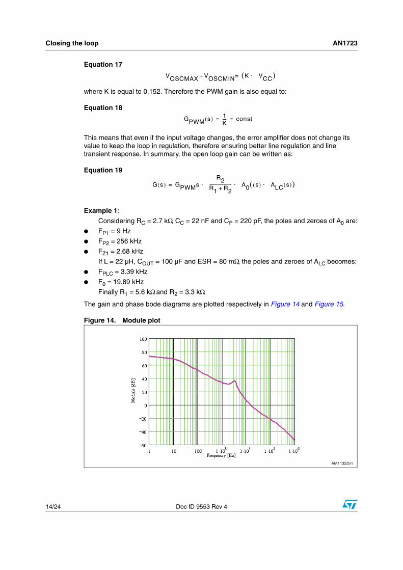
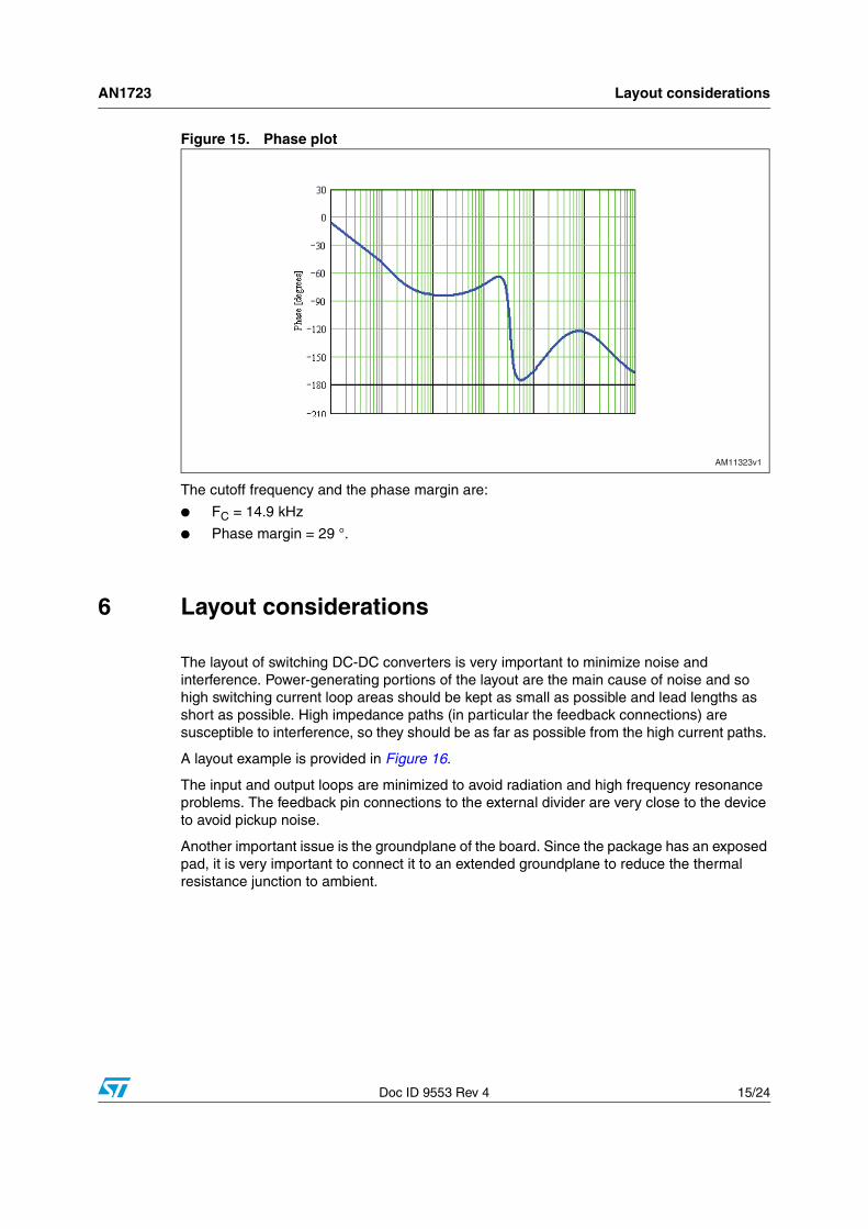
Example 1:
Considering RC = 2.7 kΩ, CC = 22 nF and CP = 220 pF, the poles and zeroes of A0 are:
● FP1 = 9 Hz
● FP2 = 256 kHz
● FZ1 = 2.68 kHz
If L = 22 µH, COUT = 100 µF and ESR = 80 mΩ, the poles and zeroes of ALC becomes:
● FPLC = 3.39 kHz
● F0 = 19.89 kHz
Finally R1 = 5.6 kΩ and R2 = 3.3 kΩ.
The gain and phase bode diagrams are plotted respectively in Figure 14 and Figure 15.
Figure 14. Module plot
VOSCMAX VOSCMIN K VCC⋅( )=–
GPWM s( ) 1K---- const= =
G s( ) GPWMsR2
R1 R2+---------------------- A0⋅ ⋅ s( ) ALC s( )⋅( )=
AM11322v1
AN1723 Layout considerations
Doc ID 9553 Rev 4 15/24
Figure 15. Phase plot
The cutoff frequency and the phase margin are:
● FC = 14.9 kHz
● Phase margin = 29 °.
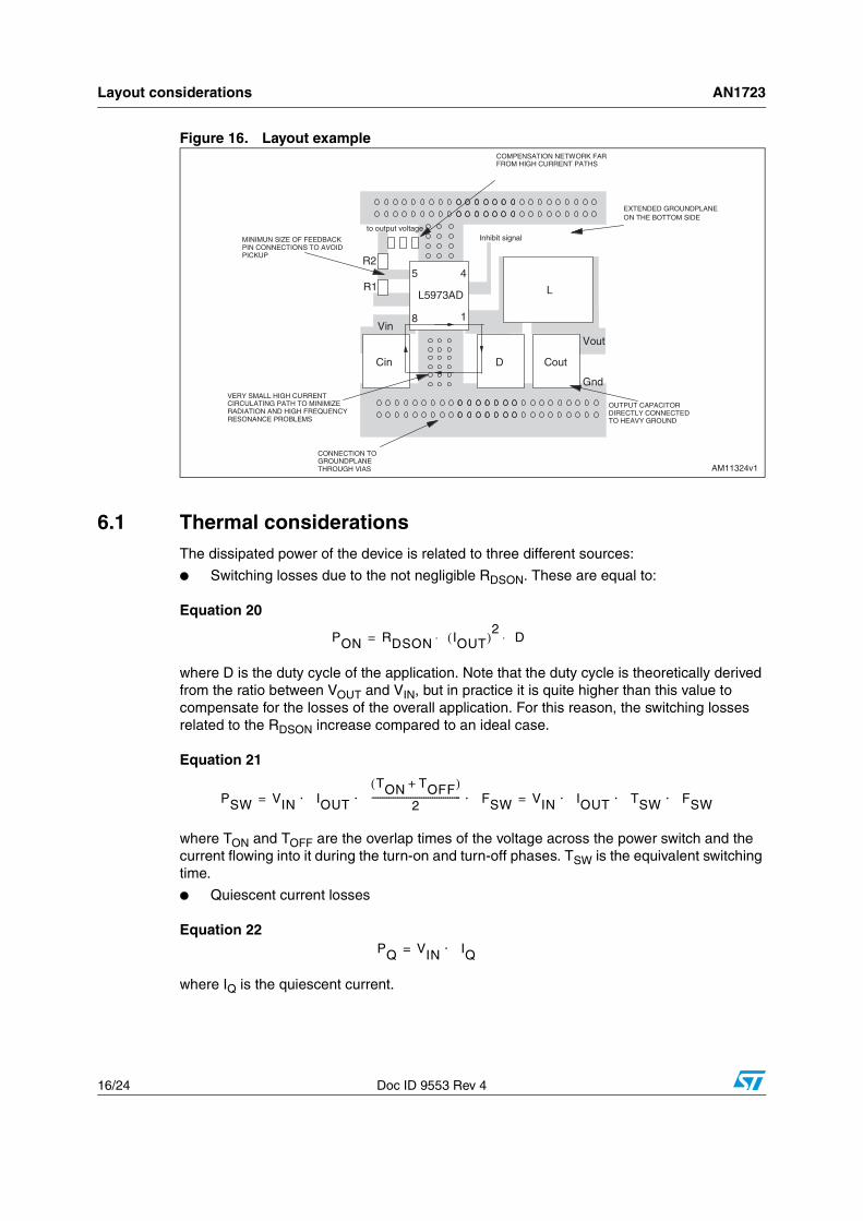
6 Layout considerations
The layout of switching DC-DC converters is very important to minimize noise and interference. Power-generating portions of the layout are the main cause of noise and so high switching current loop areas should be kept as small as possible and lead lengths as short as possible. High impedance paths (in particular the feedback connections) are susceptible to interference, so they should be as far as possible from the high current paths.
A layout example is provided in Figure 16.
The input and output loops are minimized to avoid radiation and high frequency resonance problems. The feedback pin connections to the external divider are very close to the device to avoid pickup noise.
Another important issue is the groundplane of the board. Since the package has an exposed pad, it is very important to connect it to an extended groundplane to reduce the thermal resistance junction to ambient.
AM11323v1
Layout considerations AN1723
16/24 Doc ID 9553 Rev 4
Figure 16. Layout example
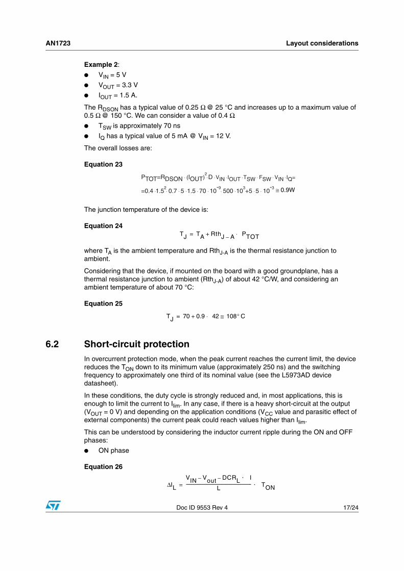
6.1 Thermal considerationsThe dissipated power of the device is related to three different sources:
● Switching losses due to the not negligible RDSON. These are equal to:
Equation 20
where D is the duty cycle of the application. Note that the duty cycle is theoretically derived from the ratio between VOUT and VIN, but in practice it is quite higher than this value to compensate for the losses of the overall application. For this reason, the switching losses related to the RDSON increase compared to an ideal case.
Equation 21
where TON and TOFF are the overlap times of the voltage across the power switch and the current flowing into it during the turn-on and turn-off phases. TSW is the equivalent switching time.
● Quiescent current losses
Equation 22
where IQ is the quiescent current.
AM11324v1
L5973AD
Cin D Cout
L
Inhibit signalto output voltage
VinVout
Gnd
R1
R2
1
45
8
VERY SMALL HIGH CURRENT CIRCULATING PATH TO MINIMIZE RADIATION AND HIGH FREQUENCY RESONANCE PROBLEMS
OUTPUT CAPACITOR DIRECTLY CONNECTED TO HEAVY GROUND
COMPENSATION NETWORK FAR FROM HIGH CURRENT PATHS
MINIMUN SIZE OF FEEDBACK PIN CONNECTIONS TO AVOID PICKUP
CONNECTION TO GROUNDPLANE THROUGH VIAS
EXTENDED GROUNDPLANEON THE BOTTOM SIDE
PON RDSON IOUT( )2 D⋅ ⋅=
PSW VIN IOUT
TON TOFF+( )
2----------------------------------------- FSW⋅ ⋅ ⋅ VIN IOUT TSW FSW⋅ ⋅ ⋅= =
PQ VIN IQ⋅=
AN1723 Layout considerations
Doc ID 9553 Rev 4 17/24
Example 2:
● VIN = 5 V
● VOUT = 3.3 V
● IOUT = 1.5 A.
The RDSON has a typical value of 0.25 Ω @ 25 °C and increases up to a maximum value of 0.5 Ω @ 150 °C. We can consider a value of 0.4 Ω.
● TSW is approximately 70 ns
● IQ has a typical value of 5 mA @ VIN = 12 V.
The overall losses are:
Equation 23
The junction temperature of the device is:
Equation 24
where TA is the ambient temperature and RthJ-A is the thermal resistance junction to ambient.
Considering that the device, if mounted on the board with a good groundplane, has a thermal resistance junction to ambient (RthJ-A) of about 42 °C/W, and considering an ambient temperature of about 70 °C:
Equation 25
6.2 Short-circuit protectionIn overcurrent protection mode, when the peak current reaches the current limit, the device reduces the TON down to its minimum value (approximately 250 ns) and the switching frequency to approximately one third of its nominal value (see the L5973AD device datasheet).
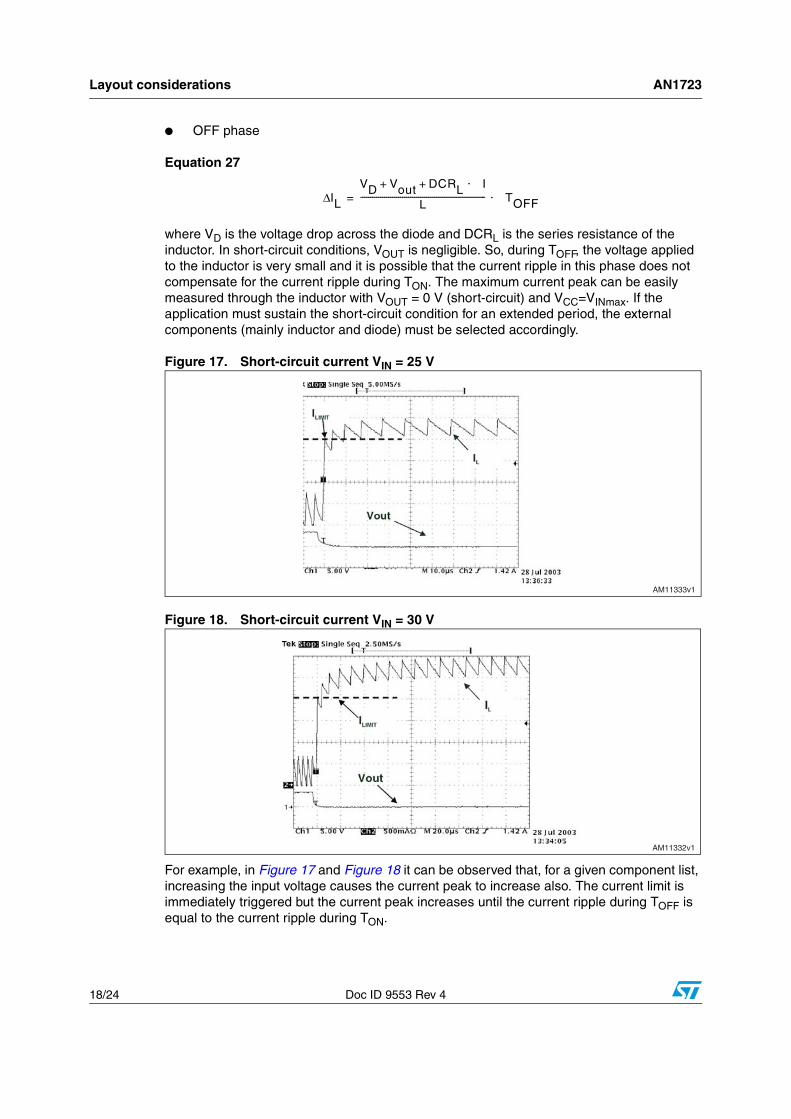
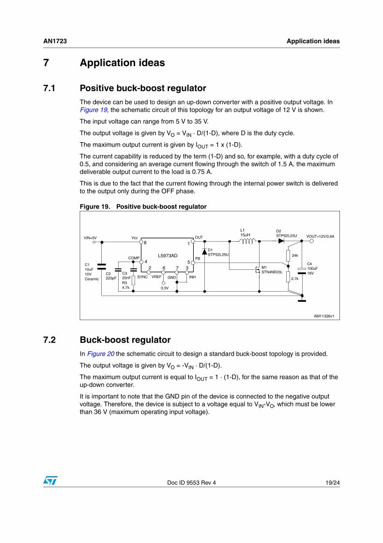
In these conditions, the duty cycle is strongly reduced and, in most applications, this is enough to limit the current to Ilim. In any case, if there is a heavy short-circuit at the output (VOUT = 0 V) and depending on the application conditions (VCC value and parasitic effect of external components) the current peak could reach values higher than Ilim.
This can be understood by considering the inductor current ripple during the ON and OFF phases:
● ON phase
Equation 26
PTOT=RDSON • (IOUT)2
• D • VIN • IOUT • TSW • FSW • VIN • IQ=
=0.4 •1.52
• 0.7 • 5 • 1.5 • 70 • 10-9
• 500 • 103+5 • 5 • 10
-3 ≅ 0.9W
TJ TA RthJ A– PTOT⋅+=
TJ 70 0.9 42 108° C≅⋅+=
ILΔVIN Vout DCRL I⋅––
L---------------------------------------------------------------- TON⋅=
Layout considerations AN1723
18/24 Doc ID 9553 Rev 4
● OFF phase
Equation 27
where VD is the voltage drop across the diode and DCRL is the series resistance of the inductor. In short-circuit conditions, VOUT is negligible. So, during TOFF, the voltage applied to the inductor is very small and it is possible that the current ripple in this phase does not compensate for the current ripple during TON. The maximum current peak can be easily measured through the inductor with VOUT = 0 V (short-circuit) and VCC=VINmax. If the application must sustain the short-circuit condition for an extended period, the external components (mainly inductor and diode) must be selected accordingly.
Figure 17. Short-circuit current VIN = 25 V
Figure 18. Short-circuit current VIN = 30 V
For example, in Figure 17 and Figure 18 it can be observed that, for a given component list, increasing the input voltage causes the current peak to increase also. The current limit is immediately triggered but the current peak increases until the current ripple during TOFF is equal to the current ripple during TON.
ILΔVD Vout DCRL I⋅+ +
L--------------------------------------------------------------- TOFF⋅=
AM11333v1
AM11332v1
AN1723 Application ideas
Doc ID 9553 Rev 4 19/24
7 Application ideas
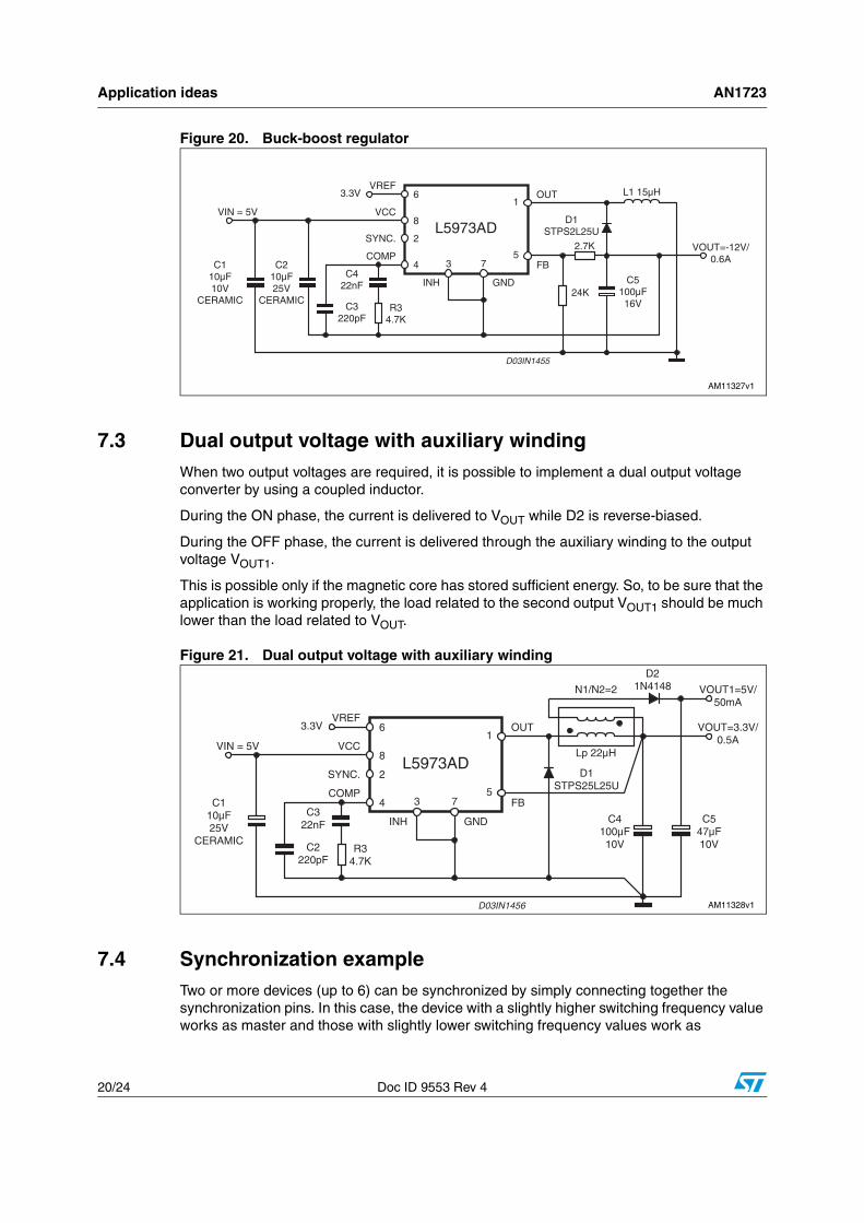
7.1 Positive buck-boost regulatorThe device can be used to design an up-down converter with a positive output voltage. In Figure 19, the schematic circuit of this topology for an output voltage of 12 V is shown.
The input voltage can range from 5 V to 35 V.
The output voltage is given by VO = VIN · D/(1-D), where D is the duty cycle.
The maximum output current is given by IOUT = 1 x (1-D).
The current capability is reduced by the term (1-D) and so, for example, with a duty cycle of 0.5, and considering an average current flowing through the switch of 1.5 A, the maximum deliverable output current to the load is 0.75 A.
This is due to the fact that the current flowing through the internal power switch is delivered to the output only during the OFF phase.
Figure 19. Positive buck-boost regulator
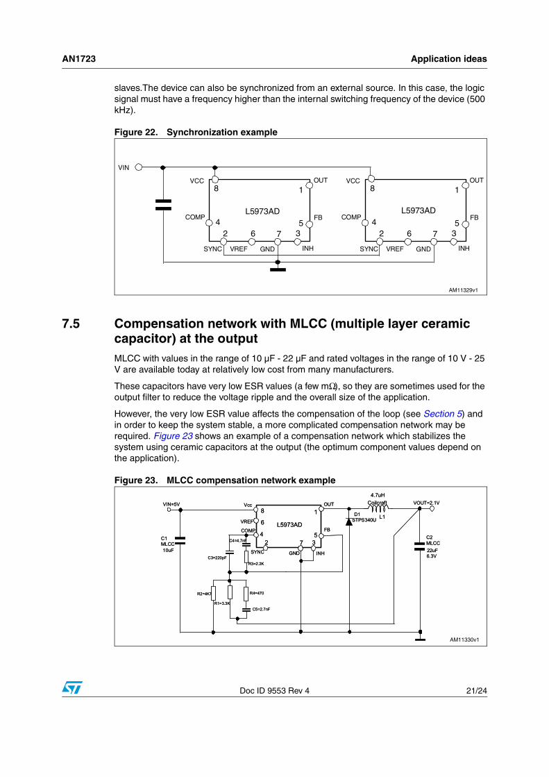
7.2 Buck-boost regulatorIn Figure 20 the schematic circuit to design a standard buck-boost topology is provided.
The output voltage is given by VO = -VIN · D/(1-D).
The maximum output current is equal to IOUT = 1 · (1-D), for the same reason as that of the up-down converter.
It is important to note that the GND pin of the device is connected to the negative output voltage. Therefore, the device is subject to a voltage equal to VIN-VO, which must be lower than 36 V (maximum operating input voltage).
VIN=5V
C110uF10VCeramic
D1STPS2L25U
Vcc
COMP
GND
OUT
FB
INHSYNC VREF
L5973AD
1
375
64
8
2
R34.7k
L1 15uH
24k
2.7kC322nF
3.3V
C4100uF16V
VOUT=12V/0.6A
C2220pF
D2STPS2L25U
M1STN4NE03L
AM11326v1
Application ideas AN1723
20/24 Doc ID 9553 Rev 4
Figure 20. Buck-boost regulator
7.3 Dual output voltage with auxiliary windingWhen two output voltages are required, it is possible to implement a dual output voltage converter by using a coupled inductor.
During the ON phase, the current is delivered to VOUT while D2 is reverse-biased.
During the OFF phase, the current is delivered through the auxiliary winding to the output voltage VOUT1.
This is possible only if the magnetic core has stored sufficient energy. So, to be sure that the application is working properly, the load related to the second output VOUT1 should be much lower than the load related to VOUT.
Figure 21. Dual output voltage with auxiliary winding
7.4 Synchronization exampleTwo or more devices (up to 6) can be synchronized by simply connecting together the synchronization pins. In this case, the device with a slightly higher switching frequency value works as master and those with slightly lower switching frequency values work as
AM11327v1
D03IN1455
8
45
1
7
L5973AD
C110µF10V
CERAMIC
C210µF25V
CERAMIC
C5100µF16V
VOUT=-12V/0.6A
VIN = 5V
2.7K
24K
R34.7K
C422nF
C3220pF
3
L1 15µH
D1STPS2L25U
COMP
VCC
OUT
FB
GNDINH
2
63.3V
SYNC.
VREF
AM11328v1D03IN1456
8
45
1
7
L5973AD
C110µF25V
CERAMIC
C547µF10V
C4100µF10V
VOUT=3.3V/0.5A
VOUT1=5V/50mA
VIN = 5V
R34.7K
C322nF
C2220pF
3
Lp 22µH
N1/N2=2
D1STPS25L25U
D21N4148
COMP
VCC
OUT
FB
GNDINH
2
63.3V
SYNC.
VREF
AN1723 Application ideas
Doc ID 9553 Rev 4 21/24
slaves.The device can also be synchronized from an external source. In this case, the logic signal must have a frequency higher than the internal switching frequency of the device (500 kHz).
Figure 22. Synchronization example
7.5 Compensation network with MLCC (multiple layer ceramic capacitor) at the outputMLCC with values in the range of 10 µF - 22 µF and rated voltages in the range of 10 V - 25 V are available today at relatively low cost from many manufacturers.
These capacitors have very low ESR values (a few mΩ), so they are sometimes used for the output filter to reduce the voltage ripple and the overall size of the application.
However, the very low ESR value affects the compensation of the loop (see Section 5) and in order to keep the system stable, a more complicated compensation network may be required. Figure 23 shows an example of a compensation network which stabilizes the system using ceramic capacitors at the output (the optimum component values depend on the application).
Figure 23. MLCC compensation network example
AM11329v1
VCC
GND
OUT
FB
INHSYNC VREF
1
375
64
8
2
L5973ADCOMP
VCC
GND
OUT
FB
INHSYNC VREF
1
375
64
8
2
L5973ADCOMP
VIN
AM11330v1
L1
VIN=5V
C1MLCC10uF
D1STPS340U
Vcc
COMP
GND
OUT
FB
INHSYNC
VREF
1
375
6
4
8
2
R3=2.2K
4.7uHCoilcraft
C4=4.7nFC2MLCC22uF6.3V
L5973AD
VOUT=2.1V
C5=2.7nF
R4=470
R1=3.3K
C3=220pF
R2=4K7
L1
VIN=5V
C1MLCC10uF
D1STPS340U
Vcc
COMP
GND
OUT
FB
INHSYNC
VREF
1
375
6
4
8
2
R3=2.2K
4.7uHCoilcraft
C4=4.7nFC2MLCC22uF6.3V
L5973AD
VOUT=2.1V
C5=2.7nF
R4=470
R1=3.3K
C3=220pF
R2=4K7
Application ideas AN1723
22/24 Doc ID 9553 Rev 4
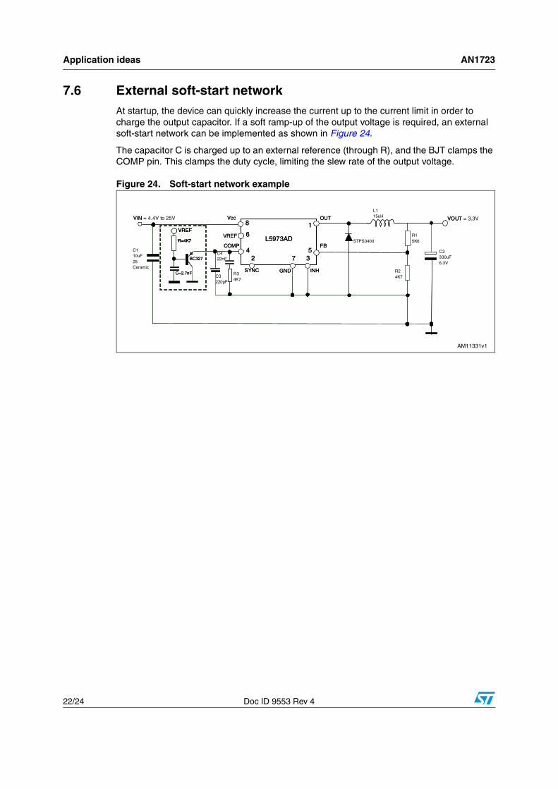
7.6 External soft-start networkAt startup, the device can quickly increase the current up to the current limit in order to charge the output capacitor. If a soft ramp-up of the output voltage is required, an external soft-start network can be implemented as shown in Figure 24.
The capacitor C is charged up to an external reference (through R), and the BJT clamps the COMP pin. This clamps the duty cycle, limiting the slew rate of the output voltage.
Figure 24. Soft-start network example
AM11331v1
VIN Vcc
COMP
GND
OUT
FB
INHSYNC
VREF
1
375
6
4
8
2
L5973AD
VOUT
VREF
R=4K7
C=2.7nF
BC327
VIN = 4.4V to 25V Vcc
COMP
GND
OUT
FB
INHSYNC
VREF
1
375
6
4
8
2
L5973AD
VOUT = 3.3V
VREF
R=4K7
VREF
R=4K7
C=2.7nF
BC327
C110uF25Ceramic
C422nF
C3220pF
R34K7
R15K6
R24K7
L115uH
STPS3400
C2330uF6.3V
AN1723 Revision history
Doc ID 9553 Rev 4 23/24
8 Revision history
Table 5. Document revision history
Date Revision Changes
18-Oct-2006 2 Initial electronic version
09-Jun-2009 3– Section 5: Closing the loop modified
– Minor text changes throughout the document
07-Jun-2012 4Equations: 4, 5, 20, 21, 22, 23, 24, 25, 26 and 27 have been updated.
AN1723
24/24 Doc ID 9553 Rev 4
Please Read Carefully:
Information in this document is provided solely in connection with ST products. STMicroelectronics NV and its subsidiaries (“ST”) reserve theright to make changes, corrections, modifications or improvements, to this document, and the products and services described herein at anytime, without notice.
All ST products are sold pursuant to ST’s terms and conditions of sale.
Purchasers are solely responsible for the choice, selection and use of the ST products and services described herein, and ST assumes noliability whatsoever relating to the choice, selection or use of the ST products and services described herein.
No license, express or implied, by estoppel or otherwise, to any intellectual property rights is granted under this document. If any part of thisdocument refers to any third party products or services it shall not be deemed a license grant by ST for the use of such third party productsor services, or any intellectual property contained therein or considered as a warranty covering the use in any manner whatsoever of suchthird party products or services or any intellectual property contained therein.
UNLESS OTHERWISE SET FORTH IN ST’S TERMS AND CONDITIONS OF SALE ST DISCLAIMS ANY EXPRESS OR IMPLIEDWARRANTY WITH RESPECT TO THE USE AND/OR SALE OF ST PRODUCTS INCLUDING WITHOUT LIMITATION IMPLIEDWARRANTIES OF MERCHANTABILITY, FITNESS FOR A PARTICULAR PURPOSE (AND THEIR EQUIVALENTS UNDER THE LAWSOF ANY JURISDICTION), OR INFRINGEMENT OF ANY PATENT, COPYRIGHT OR OTHER INTELLECTUAL PROPERTY RIGHT.
UNLESS EXPRESSLY APPROVED IN WRITING BY TWO AUTHORIZED ST REPRESENTATIVES, ST PRODUCTS ARE NOTRECOMMENDED, AUTHORIZED OR WARRANTED FOR USE IN MILITARY, AIR CRAFT, SPACE, LIFE SAVING, OR LIFE SUSTAININGAPPLICATIONS, NOR IN PRODUCTS OR SYSTEMS WHERE FAILURE OR MALFUNCTION MAY RESULT IN PERSONAL INJURY,DEATH, OR SEVERE PROPERTY OR ENVIRONMENTAL DAMAGE. ST PRODUCTS WHICH ARE NOT SPECIFIED AS "AUTOMOTIVEGRADE" MAY ONLY BE USED IN AUTOMOTIVE APPLICATIONS AT USER’S OWN RISK.
Resale of ST products with provisions different from the statements and/or technical features set forth in this document shall immediately voidany warranty granted by ST for the ST product or service described herein and shall not create or extend in any manner whatsoever, anyliability of ST.
ST and the ST logo are trademarks or registered trademarks of ST in various countries.
Information in this document supersedes and replaces all information previously supplied.
The ST logo is a registered trademark of STMicroelectronics. All other names are the property of their respective owners.
© 2012 STMicroelectronics - All rights reserved
STMicroelectronics group of companies
Australia - Belgium - Brazil - Canada - China - Czech Republic - Finland - France - Germany - Hong Kong - India - Israel - Italy - Japan - Malaysia - Malta - Morocco - Philippines - Singapore - Spain - Sweden - Switzerland - United Kingdom - United States of America
www.st.com