Embed Size (px)
Citation preview
1
ABTAdvanced BiCMOS Technology
Characterization Information
SCBA008BJune 1997
2
IMPORTANT NOTICE
Texas Instruments (TI) reserves the right to make changes to its products or to discontinue anysemiconductor product or service without notice, and advises its customers to obtain the latestversion of relevant information to verify, before placing orders, that the information being reliedon is current.
TI warrants performance of its semiconductor products and related software to the specificationsapplicable at the time of sale in accordance with TI’s standard warranty. Testing and other qualitycontrol techniques are utilized to the extent TI deems necessary to support this warranty.Specific testing of all parameters of each device is not necessarily performed, except thosemandated by government requirements.
Certain applications using semiconductor products may involve potential risks of death,personal injury, or severe property or environmental damage (“Critical Applications”).
TI SEMICONDUCTOR PRODUCTS ARE NOT DESIGNED, INTENDED, AUTHORIZED, ORWARRANTED TO BE SUITABLE FOR USE IN LIFE-SUPPORT APPLICATIONS, DEVICESOR SYSTEMS OR OTHER CRITICAL APPLICATIONS.
Inclusion of TI products in such applications is understood to be fully at the risk of the customer.Use of TI products in such applications requires the written approval of an appropriate TI officer.Questions concerning potential risk applications should be directed to TI through a local SCsales office.
In order to minimize risks associated with the customer’s applications, adequate design andoperating safeguards should be provided by the customer to minimize inherent orprocedural hazards.
TI assumes no liability for applications assistance, customer product design, softwareperformance, or infringement of patents or services described herein. Nor does TI warrant orrepresent that any license, either express or implied, is granted under any patent right, copyright,mask work right, or other intellectual property right of TI covering or relating to any combination,machine, or process in which such semiconductor products or services might be or are used.
Copyright 1997, Texas Instruments Incorporated

iii
ContentsTitle Page
Introduction 1. . . . . . . . . . . . . . . . . . . . . . . . . . . . . . . . . . . . . . . . . . . . . . . . . . . . . . . . . . . . . . . . . . . . . . . . . . . . . . . . . . . . . . .
AC Performance 1. . . . . . . . . . . . . . . . . . . . . . . . . . . . . . . . . . . . . . . . . . . . . . . . . . . . . . . . . . . . . . . . . . . . . . . . . . . . . . . . . . .
Power Considerations 6. . . . . . . . . . . . . . . . . . . . . . . . . . . . . . . . . . . . . . . . . . . . . . . . . . . . . . . . . . . . . . . . . . . . . . . . . . . . . . .
Input Characteristics 7. . . . . . . . . . . . . . . . . . . . . . . . . . . . . . . . . . . . . . . . . . . . . . . . . . . . . . . . . . . . . . . . . . . . . . . . . . . . . . . . ABT Input Circuitry 7. . . . . . . . . . . . . . . . . . . . . . . . . . . . . . . . . . . . . . . . . . . . . . . . . . . . . . . . . . . . . . . . . . . . . . . . . . . . .
Input Current Loading 8. . . . . . . . . . . . . . . . . . . . . . . . . . . . . . . . . . . . . . . . . . . . . . . . . . . . . . . . . . . . . . . . . . . . . . . . . . . . . .
Supply Current Change (∆ICC) 9. . . . . . . . . . . . . . . . . . . . . . . . . . . . . . . . . . . . . . . . . . . . . . . . . . . . . . . . . . . . . . . . . . . . . . . Proper Termination of Unused Inputs 10. . . . . . . . . . . . . . . . . . . . . . . . . . . . . . . . . . . . . . . . . . . . . . . . . . . . . . . . . . . . . .
Output Characteristics 10. . . . . . . . . . . . . . . . . . . . . . . . . . . . . . . . . . . . . . . . . . . . . . . . . . . . . . . . . . . . . . . . . . . . . . . . . . . . . Output Drive 11. . . . . . . . . . . . . . . . . . . . . . . . . . . . . . . . . . . . . . . . . . . . . . . . . . . . . . . . . . . . . . . . . . . . . . . . . . . . . . . . . . Partial Power Down 12. . . . . . . . . . . . . . . . . . . . . . . . . . . . . . . . . . . . . . . . . . . . . . . . . . . . . . . . . . . . . . . . . . . . . . . . . . . .
Signal Integrity 13. . . . . . . . . . . . . . . . . . . . . . . . . . . . . . . . . . . . . . . . . . . . . . . . . . . . . . . . . . . . . . . . . . . . . . . . . . . . . . . . . . . . Simultaneous-Switching Phenomenon 13. . . . . . . . . . . . . . . . . . . . . . . . . . . . . . . . . . . . . . . . . . . . . . . . . . . . . . . . . . . . . . Simultaneous-Switching Solutions 15. . . . . . . . . . . . . . . . . . . . . . . . . . . . . . . . . . . . . . . . . . . . . . . . . . . . . . . . . . . . . . . .
Advanced Packaging 17. . . . . . . . . . . . . . . . . . . . . . . . . . . . . . . . . . . . . . . . . . . . . . . . . . . . . . . . . . . . . . . . . . . . . . . . . . . . . . .
List of IllustrationsFigure Title Page
1 Propagation Delay vs Operating Free-Air Temperature A to Y 2. . . . . . . . . . . . . . . . . . . . . . . . . . . . . . . . . . . . . . . . .
2 Propagation Delay vs Number of Outputs Switching 4. . . . . . . . . . . . . . . . . . . . . . . . . . . . . . . . . . . . . . . . . . . . . . . . .
3 Propagation Delay vs Capacitive Load 5. . . . . . . . . . . . . . . . . . . . . . . . . . . . . . . . . . . . . . . . . . . . . . . . . . . . . . . . . . . .
4 Supply Current vs Frequency 6. . . . . . . . . . . . . . . . . . . . . . . . . . . . . . . . . . . . . . . . . . . . . . . . . . . . . . . . . . . . . . . . . . .
5 Simplified Input Stage of an ABT Circuit 7. . . . . . . . . . . . . . . . . . . . . . . . . . . . . . . . . . . . . . . . . . . . . . . . . . . . . . . . . .
6 Output Voltage vs Input Voltage 8. . . . . . . . . . . . . . . . . . . . . . . . . . . . . . . . . . . . . . . . . . . . . . . . . . . . . . . . . . . . . . . . .
7 Input Current vs Input Voltage 8. . . . . . . . . . . . . . . . . . . . . . . . . . . . . . . . . . . . . . . . . . . . . . . . . . . . . . . . . . . . . . . . . .
8 Supply Current vs Input Voltage 9. . . . . . . . . . . . . . . . . . . . . . . . . . . . . . . . . . . . . . . . . . . . . . . . . . . . . . . . . . . . . . . . .
9 Sample Input/Output Model 10. . . . . . . . . . . . . . . . . . . . . . . . . . . . . . . . . . . . . . . . . . . . . . . . . . . . . . . . . . . . . . . . . . .
10 Simplified ABT Output Stage 11. . . . . . . . . . . . . . . . . . . . . . . . . . . . . . . . . . . . . . . . . . . . . . . . . . . . . . . . . . . . . . . . . .
11 Typical ABT Output Characteristics 11. . . . . . . . . . . . . . . . . . . . . . . . . . . . . . . . . . . . . . . . . . . . . . . . . . . . . . . . . . . . .
12 Reflected Wave Switching 12. . . . . . . . . . . . . . . . . . . . . . . . . . . . . . . . . . . . . . . . . . . . . . . . . . . . . . . . . . . . . . . . . . . . .
13 Simplified Input Structures for CMOS and ABT Devices 13. . . . . . . . . . . . . . . . . . . . . . . . . . . . . . . . . . . . . . . . . . . .
14 Example of Partial System Power Down 13. . . . . . . . . . . . . . . . . . . . . . . . . . . . . . . . . . . . . . . . . . . . . . . . . . . . . . . . .
15 Simultaneous-Switching Output Model 13. . . . . . . . . . . . . . . . . . . . . . . . . . . . . . . . . . . . . . . . . . . . . . . . . . . . . . . . . .
EPIC-ΙΙB and Widebus are trademarks of Texas Instruments Incorporated.
iv
List of Illustrations (continued)Figure Title Page
16 Simultaneous-Switching-Noise Waveform 14. . . . . . . . . . . . . . . . . . . . . . . . . . . . . . . . . . . . . . . . . . . . . . . . . . . . . . . .
17 TTL DC Noise Margin 15. . . . . . . . . . . . . . . . . . . . . . . . . . . . . . . . . . . . . . . . . . . . . . . . . . . . . . . . . . . . . . . . . . . . . . .
18 ABT646A Simultaneous-Switching Waveform 16. . . . . . . . . . . . . . . . . . . . . . . . . . . . . . . . . . . . . . . . . . . . . . . . . . . .
19 ABT16500B Simultaneous-Switching Waveform 16. . . . . . . . . . . . . . . . . . . . . . . . . . . . . . . . . . . . . . . . . . . . . . . . . .
20 24-Pin Surface-Mount Comparison 17. . . . . . . . . . . . . . . . . . . . . . . . . . . . . . . . . . . . . . . . . . . . . . . . . . . . . . . . . . . . . .
21 Distributed Pinout of ’ABT16244A 18. . . . . . . . . . . . . . . . . . . . . . . . . . . . . . . . . . . . . . . . . . . . . . . . . . . . . . . . . . . . . .
AppendixesTitle Page
Appendix A 19. . . . . . . . . . . . . . . . . . . . . . . . . . . . . . . . . . . . . . . . . . . . . . . . . . . . . . . . . . . . . . . . . . . . . . . . . . . . . . . . . . . . . . . SN54ABT646A and SN74ABT646A Characterization Data 21. . . . . . . . . . . . . . . . . . . . . . . . . . . . . . . . . . . . . . . . . . . .
Appendix B 31. . . . . . . . . . . . . . . . . . . . . . . . . . . . . . . . . . . . . . . . . . . . . . . . . . . . . . . . . . . . . . . . . . . . . . . . . . . . . . . . . . . . . . . SN54ABT16244 and SN74ABT16244A Characterization Data 33. . . . . . . . . . . . . . . . . . . . . . . . . . . . . . . . . . . . . . . . .
Appendix C 41. . . . . . . . . . . . . . . . . . . . . . . . . . . . . . . . . . . . . . . . . . . . . . . . . . . . . . . . . . . . . . . . . . . . . . . . . . . . . . . . . . . . . . . SN54ABT16500B and SN74ABT16500 Characterization Data 43. . . . . . . . . . . . . . . . . . . . . . . . . . . . . . . . . . . . . . . . . .
1
Introduction
The purpose of this document is to assist the designers of high-performance digital logic systems in using the advancedBiCMOS technology (ABT) logic family.
Detailed electrical characteristics of these bus-interface devices are provided and tables and graphs have been included tocompare specific parameters of the ABT family with those of other logic families.
In addition, typical data is provided to give the hardware designer a better understanding of how the ABT devices operate undervarious conditions.
The major subject areas covered in the report are as follows:
• AC Performance• Power Considerations• Input Characteristics• Output Characteristics• Signal Integrity• Advanced Packaging• Characterization Information
The characterization information provided is typical data and is not intended to be used as minimum or maximumspecifications, unless noted as such.
For more information on these or other TI products, please contact your local TI representative, authorized distributor, the TItechnical support hotline at 972-644-5580, or visit the TI logic home page at http://www.ti.com/sc/logic.
For a complete listing of all TI logic products, please order our logic CD-ROM (literature number SCBC001) or LogicSelection Guide (literature number SDYU001) by calling our literature response center at 1-800-477-8924.
AC Performance
As microprocessor operating frequencies increase, the period of time allotted for operations, such as memory access orarithmetic functions, decreases. With this in mind, TI developed a family of bus-interface devices – ABT – utilizing advancedBiCMOS technology. The goal of the ABT family of devices is to give system designers one bus-interface solution thatprovides high drive capability, good signal integrity, and propagation delays short enough to appear transparent with respectto overall system performance.
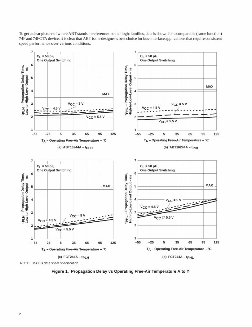
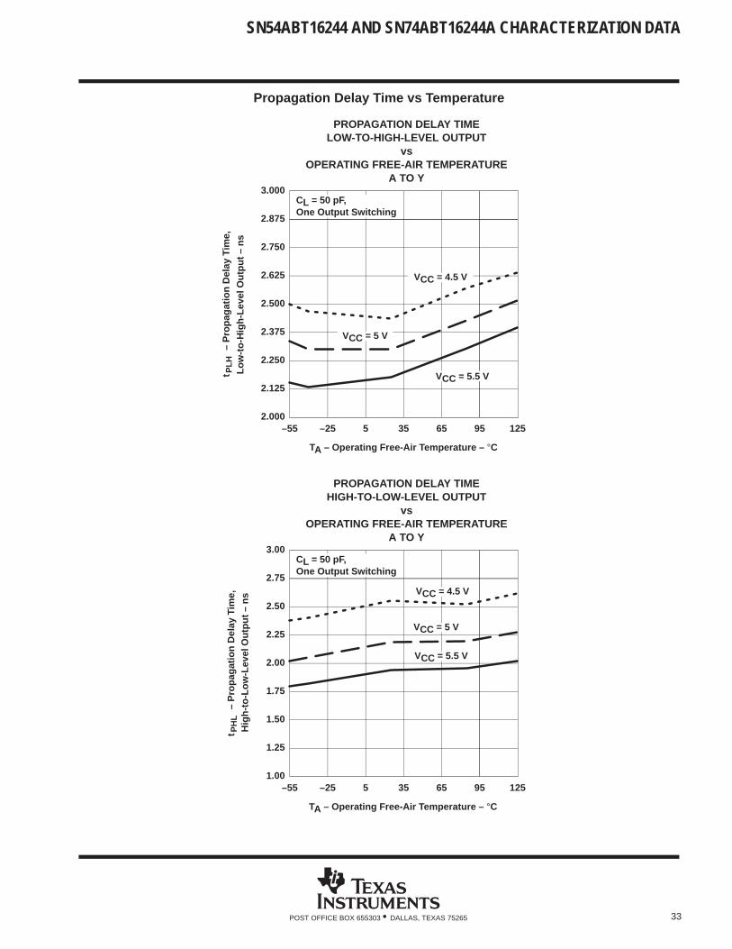
Advances in IC process technology, including smaller minimum feature size, tighter metal pitch, and shallower junctions,combine to provide stronger drive strengths and smaller parasitic capacitances. As a result, internal propagation delays havebecome extremely short. With the advent of the 0.8-µm, EPIC-IIB BiCMOS process and new circuit innovations, the ABTfamily offers typical propagation delays as low as 2-3 ns as shown in Figure 1. Maximum specifications are as low as 3–5 ns,depending on the device type.
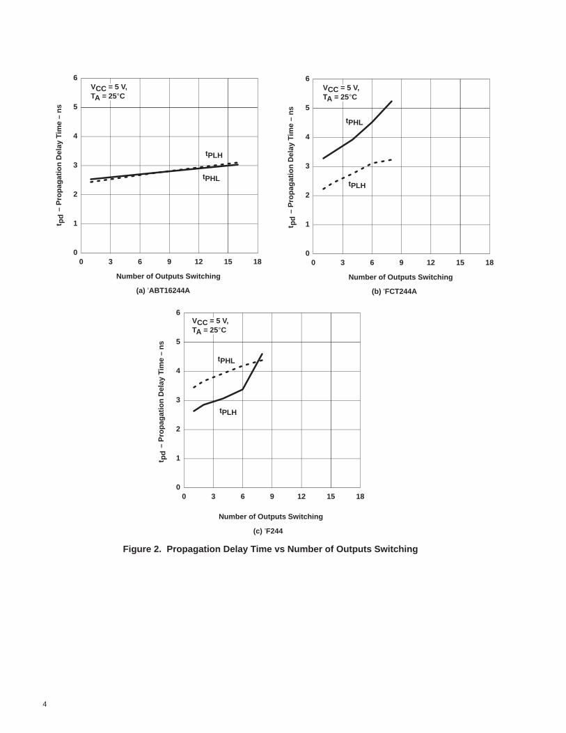
Figure 2 shows the propagation delay versus change in both temperature and supply voltage for an ’ABT16244A, ’FCT244A,and a ’F244 device. The graphs highlight two important aspects of the ABT logic family. First, ABT interface devices haveextremely short propagation delay times. The figures clearly show the improvement in speed of an ABT device over that ofa 74F and 74FCTA device. Second, the variance in speed with respect to both temperature and supply voltage is minimal forABT. At low temperatures, the increase in CMOS performance compensates for the decrease in bipolar device strength. Athigh temperatures, the reverse occurs. This complementary performance of both CMOS and bipolar devices on a single chipresults in a slope that is virtually flat across the entire temperature range of –55°C to 125°C.
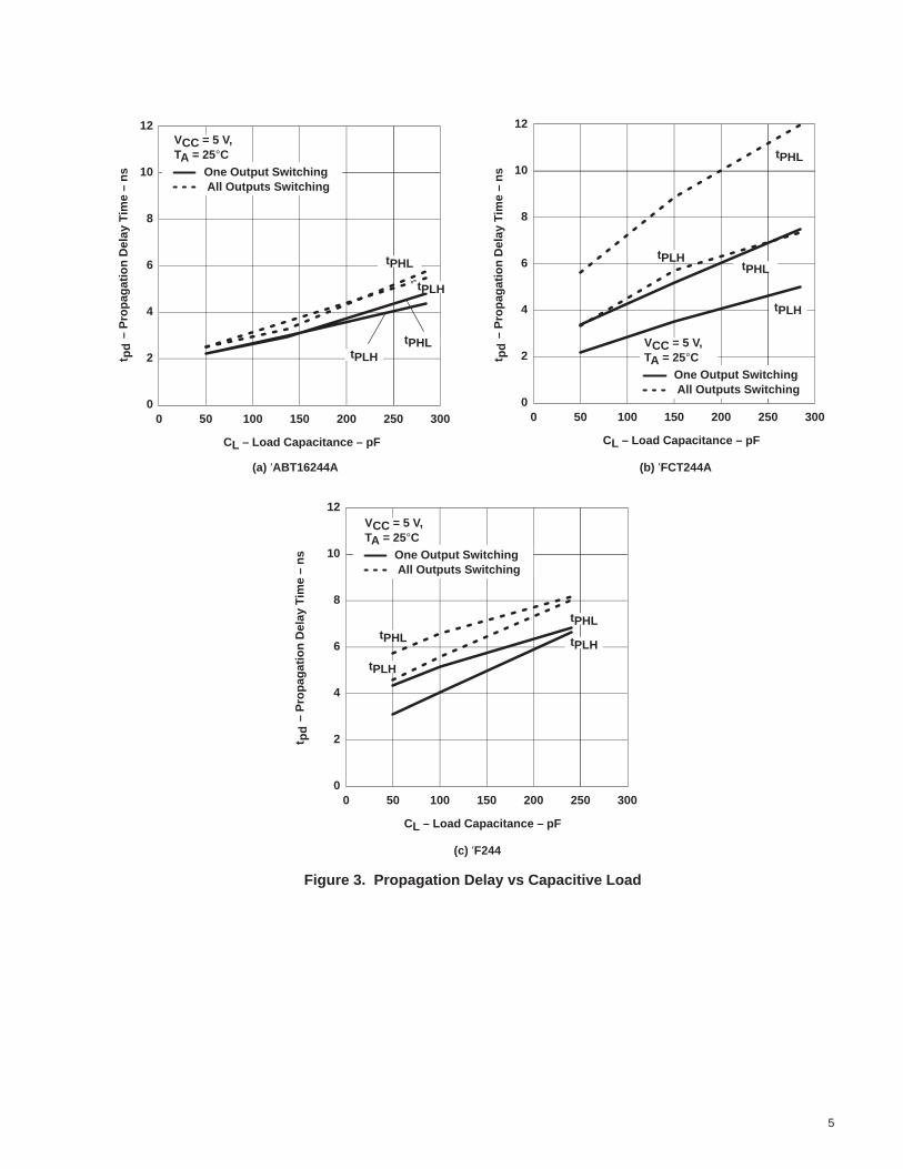
For most applications, the data sheet specifications may not provide all of the information a designer would like to see for aparticular device. For instance, a designer might benefit from data such as propagation delay with multiple outputs switchingor with various loads. This type of data is extremely difficult to test using automatic test equipment; therefore, it is providedin this document as family characteristics shown in Figure 2 and Figure 3.
2
To get a clear picture of where ABT stands in reference to other logic families, data is shown for a comparable (same function)74F and 74FCTA device. It is clear that ABT is the designer’s best choice for bus-interface applications that require consistentspeed performance over various conditions.
1
2
3
4
5
6
7
–55 –25 5 35 65 95 125
TA – Operating Free-Air Temperature – °C
MAX
t
–
Pro
paga
tion
Del
ay T
ime,
Low
-to-
Hig
h-Le
vel O
utpu
t – n
s
1
2
3
4
5
6
7
–55 –25 5 35 65 95 125
TA – Operating Free-Air Temperature – °C
MAX
1
2
3
4
5
6
7
–55 –25 5 35 65 95 125
TA – Operating Free-Air Temperature – °C
MAX
1
2
3
4
5
6
7
–55 –25 5 35 65 95 125
TA – Operating Free-Air Temperature – °C
MAX
VCC = 4.5 VVCC = 5 V
VCC = 5.5 V
VCC = 4.5 VVCC = 5 V
VCC = 5.5 V
VCC = 4.5 V
VCC = 5 V
VCC @ 5.5 V
VCC = 4.5 VVCC = 5 V
VCC = 5.5 V
PLH
t
–
Pro
paga
tion
Del
ay T
ime,
Low
-to-
Hig
h-Le
vel O
utpu
t – n
sP
LH
t
–
Pro
paga
tion
Del
ay T
ime,
Hig
h-to
-Low
-Lev
el O
utpu
t – n
sP
HL
t
–
Pro
paga
tion
Del
ay T
ime,
Hig
h-to
-Low
-Lev
el O
utpu
t – n
sP
HL
(a) ’ABT16244A – t PLH (b) ’ABT16244A – t PHL
(c) ’FCT244A – tPLH (d) ’FCT244A – tPHL
CL = 50 pF,One Output Switching
CL = 50 pF,One Output Switching
CL = 50 pF,One Output Switching
CL = 50 pF,One Output Switching
NOTE: MAX is data sheet specification
Figure 1. Propagation Delay vs Operating Free-Air Temperature A to Y
3
1
2
3
4
5
6
7
–55 –25 5 35 65 95 125
TA – Operating Free-Air Temperature – °C
MAX
1
2
3
4
5
6
7
–55 –25 5 35 65 95 125
TA – Operating Free-Air Temperature – °C
MAX
VCC = 4.5 V
VCC = 5 V
VCC = 5.5 V VCC = 4.5 V
VCC = 5 V
VCC = 5.5 V
t
–
Pro
paga
tion
Del
ay T
ime,
Low
-to-
Hig
h-Le
vel O
utpu
t – n
sP
LH
t
–
Pro
paga
tion
Del
ay T
ime,
Hig
h-to
-Low
-Lev
el O
utpu
t – n
sP
HL
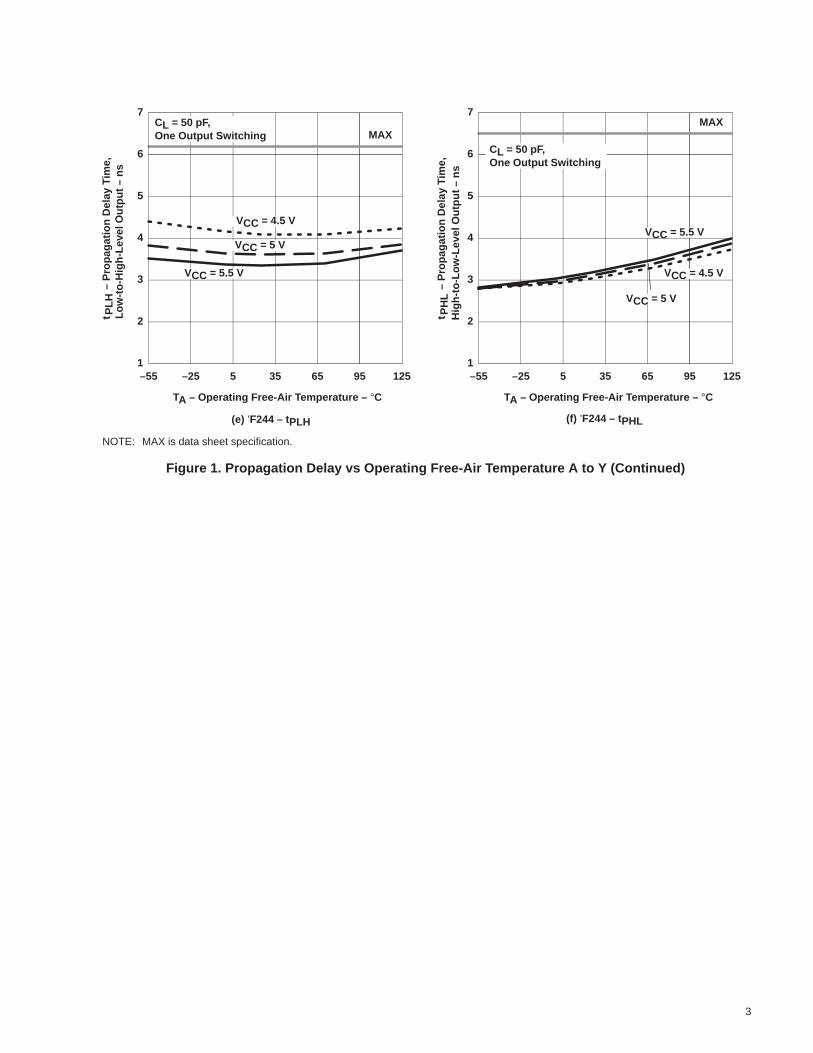
(e) ’F244 – tPLH (f) ’F244 – tPHL
CL = 50 pF,One Output Switching
CL = 50 pF,One Output Switching
NOTE: MAX is data sheet specification.
Figure 1. Propagation Delay vs Operating Free-Air Temperature A to Y (Continued)
4
0
1
2
3
4
5
6
0 3 6 9 12 15 18
Number of Outputs Switching
tPLH
tPHL
0
1
2
3
4
5
6
0 3 6 9 12 15 18
Number of Outputs Switching
tPLH
tPHL
0
1
2
3
4
5
6
0 3 6 9 12 15 18
Number of Outputs Switching
tPLH
tPHL
(a) ’ABT16244A (b) ’FCT244A
(c) ’F244
t
– P
ropa
gatio
n D
elay
Tim
e –
nspd
t
– P
ropa
gatio
n D
elay
Tim
e –
nspd
t
– P
ropa
gatio
n D
elay
Tim
e –
nspd
VCC = 5 V,TA = 25°C
VCC = 5 V,TA = 25°C
VCC = 5 V,TA = 25°C
Figure 2. Propagation Delay Time vs Number of Outputs Switching
5
0
2
4
6
8
10
12
0 50 100 150 200 250 300
CL – Load Capacitance – pF
tPLH
tPHL
0
2
4
6
8
10
12
0 50 100 150 200 250 300
CL – Load Capacitance – pF
tPLH
tPHL
0
2
4
6
8
10
12
0 50 100 150 200 250 300
CL – Load Capacitance – pF
tPHL
tPLHtPHL
tPLH
tPHL
tPLH
tPHL
t
– P
ropa
gatio
n D
elay
Tim
e –
nspd t
– P
ropa
gatio
n D
elay
Tim
e –
nspd
t
– P
ropa
gatio
n D
elay
Tim
e –
nspd
(a) ’ABT16244A (b) ’FCT244A
(c) ’F244
One Output Switching All Outputs Switching
VCC = 5 V,TA = 25°C
tPLH
One Output Switching All Outputs Switching
VCC = 5 V,TA = 25°C
One Output Switching All Outputs Switching
VCC = 5 V,TA = 25°C
Figure 3. Propagation Delay vs Capacitive Load
6
Power Considerations
With the challenge to make systems more dense while improving performance comes the need to replace power-hungry deviceswithout compromising speed. The ABT family of drivers provides a solution with low CMOS power consumption andhigh-speed bipolar technology on a single device.
There are two basic things to consider when calculating power consumption, static (dc) power, and dynamic power. Staticpower is calculated using the value of ICC as shown in the data sheet. This is a dc value with no load on the outputs. Tounderstand the relationship between pure CMOS, pure bipolar, and advanced BiCMOS for dc power rating, see Table 1, whichshows the various data sheet values. The bipolar device shows the highest ICC values, with little relief, regardless of the stateof the outputs. This is not the case with ABT octals, which offer the low static power consumption of CMOS while in thehigh-impedance state, or when the outputs are high (ICCZ, ICCH).
Table 1. Supply Current
PARAMETER TEST CONDITIONS’F244 ’FCT244 SN74ABT244
PARAMETER TEST CONDITIONSMIN MAX MIN MAX MIN MAX
Outputs high 60 mA 250 µA
ICCVCC = 5.5 V, IO = 0, VI = VCC or GND Outputs low 90 mA 30 mA
ICCOutputs disabled 90 mA 250 µA
VCC = maximum, V ≥ VCC – 0.2 V, V ≤ VCC – 0.2 V 1.5 mA
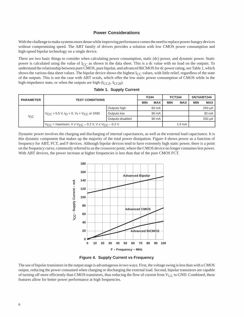
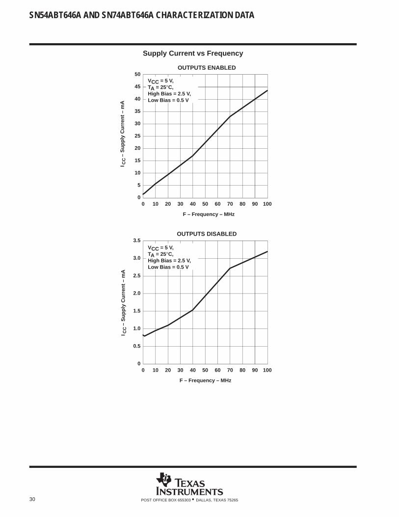
Dynamic power involves the charging and discharging of internal capacitances, as well as the external load capacitance. It isthis dynamic component that makes up the majority of the total power dissipation. Figure 4 shows power as a function offrequency for ABT, FCT, and F devices. Although bipolar devices tend to have extremely high static power, there is a pointon the frequency curve, commonly referred to as the crossover point, where the CMOS device no longer consumes less power.With ABT devices, the power increase at higher frequencies is less than that of the pure CMOS FCT.
0
20
40
60
80
100
120
140
160
180
0 10 20 30 40 50 60 70 80 90 100
F – Frequency – MHz
Advanced Bipolar
Advanced BiCMOS
Advanced CMOS
– S
uppl
y C
urre
nt –
mA
CC
I
Figure 4. Supply Current vs Frequency
The use of bipolar transistors in the output stage is advantageous in two ways. First, the voltage swing is less than with a CMOSoutput, reducing the power consumed when charging or discharging the external load. Second, bipolar transistors are capableof turning off more efficiently than CMOS transistors, thus reducing the flow of current from VCC to GND. Combined, thesefeatures allow for better power performance at high frequencies.
7
Input Characteristics
ABT bus-interface devices are designed to ensure TTL-compatible input levels switching between 0.8 V and 2 V (typically1.5 V). Additionally, these inputs are implemented with CMOS circuitry, resulting in high impedance (low leakage) and lowcapacitance, which reduces overall bus loading. This section is an overview of the circuitry utilized for a typical ABT input,the corresponding electrical characteristics, and guidelines for proper termination of unused inputs.
ABT Input Circuitry
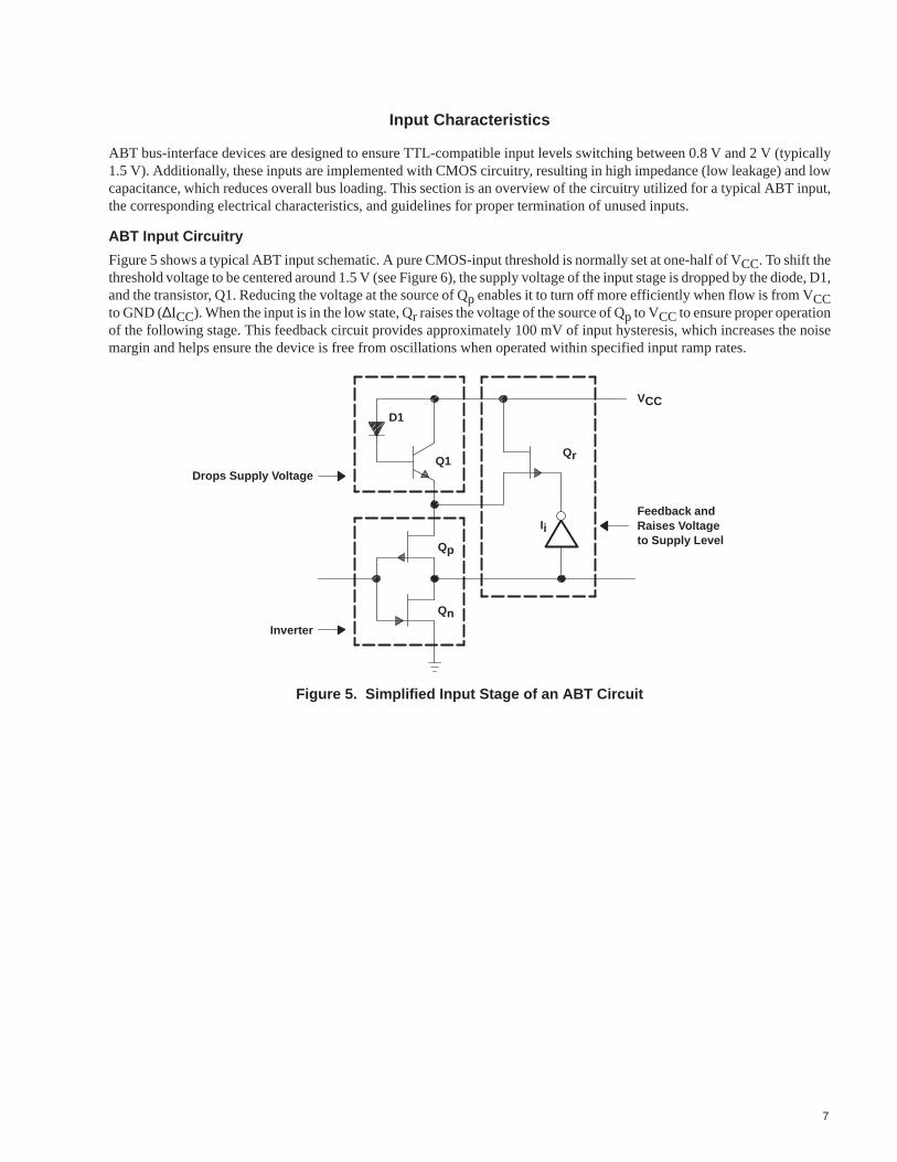
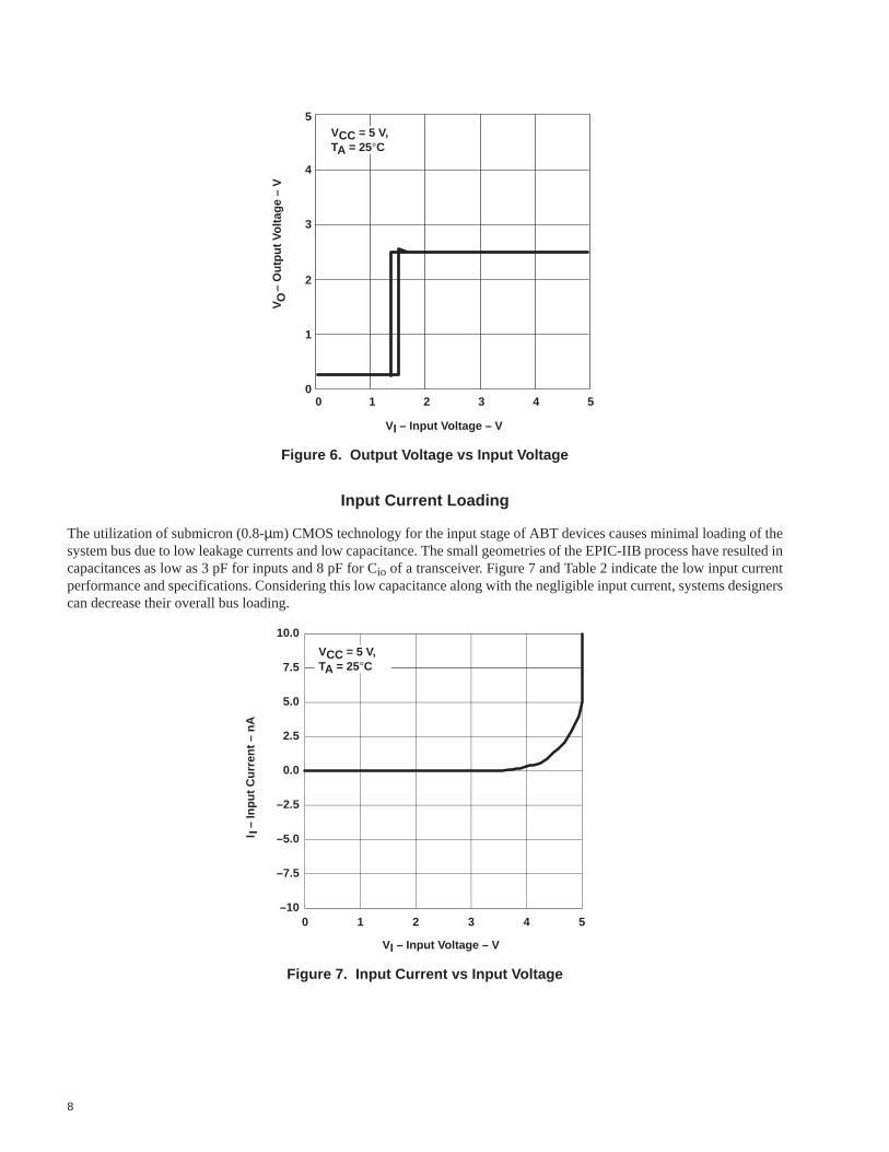
Figure 5 shows a typical ABT input schematic. A pure CMOS-input threshold is normally set at one-half of VCC. To shift thethreshold voltage to be centered around 1.5 V (see Figure 6), the supply voltage of the input stage is dropped by the diode, D1,and the transistor, Q1. Reducing the voltage at the source of Qp enables it to turn off more efficiently when flow is from VCCto GND (∆ICC). When the input is in the low state, Qr raises the voltage of the source of Qp to VCC to ensure proper operationof the following stage. This feedback circuit provides approximately 100 mV of input hysteresis, which increases the noisemargin and helps ensure the device is free from oscillations when operated within specified input ramp rates.
D1
Q1
Qp
Qn
Qr
Ii
VCC
Feedback andRaises Voltageto Supply Level
Drops Supply Voltage
Inverter
Figure 5. Simplified Input Stage of an ABT Circuit
8
3
2
1
00 1 2 3
4
5
4 5
V
– O
utpu
t Vol
tage
– V
O
VI – Input Voltage – V
VCC = 5 V,TA = 25°C
Figure 6. Output Voltage vs Input Voltage
Input Current Loading
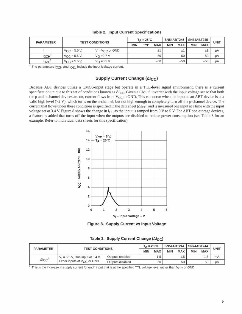
The utilization of submicron (0.8-µm) CMOS technology for the input stage of ABT devices causes minimal loading of thesystem bus due to low leakage currents and low capacitance. The small geometries of the EPIC-IIB process have resulted incapacitances as low as 3 pF for inputs and 8 pF for Cio of a transceiver. Figure 7 and Table 2 indicate the low input currentperformance and specifications. Considering this low capacitance along with the negligible input current, systems designerscan decrease their overall bus loading.
–10
–7.5
–5.0
–2.5
0.0
2.5
5.0
7.5
10.0
0 1 2 3 4 5
– In
put C
urre
nt –
nA
VI – Input Voltage – V
I I
VCC = 5 V,TA = 25°C
Figure 7. Input Current vs Input Voltage
9
Table 2. Input Current Specifications
PARAMETER TEST CONDITIONSTA = 25°C SN54ABT245 SN74ABT245
UNITPARAMETER TEST CONDITIONSMIN TYP MAX MIN MAX MIN MAX
UNIT
II VCC = 5.5 V, VI =VCC or GND ±1 ±1 ±1 µA
IOZH† VCC = 5.5 V, VO =2.7 V 50 50 50 µA
IOZL† VCC = 5.5 V, VO =0.5 V –50 –50 –50 µA
† The parameters IOZH and IOZL include the input leakage current.
Supply Current Change ( ∆ICC)
Because ABT devices utilize a CMOS-input stage but operate in a TTL-level signal environment, there is a currentspecification unique to this set of conditions known as ∆ICC. Given a CMOS inverter with the input voltage set so that boththe p and n channel devices are on, current flows from VCC to GND. This can occur when the input to an ABT device is at avalid high level (>2 V), which turns on the n-channel, but not high enough to completely turn off the p-channel device. Thecurrent that flows under these conditions is specified in the data sheet (∆ICC) and is measured one input at a time with the inputvoltage set at 3.4 V. Figure 8 shows the change in ICC as the input is ramped from 0 V to 5 V. For ABT non-storage devices,a feature is added that turns off the input when the outputs are disabled to reduce power consumption (see Table 3 for anexample. Refer to individual data sheets for this specification).
0
2
4
6
8
10
12
14
16
0 1 2 3 4 5 6
VI – Input Voltage – V
– S
uppl
y C
urre
nt –
mA
CC
I
VCC = 5 V,TA = 25°C
Figure 8. Supply Current vs Input Voltage
Table 3. Supply Current Change ( ∆ICC)
PARAMETER TEST CONDITIONSTA = 25°C SN54ABT244 SN74ABT244
UNITPARAMETER TEST CONDITIONSMIN MAX MIN MAX MIN MAX
UNIT
∆ICC† VI = 5.5 V, One input at 3.4 V, Outputs enabled 1.5 1.5 1.5 mA∆ICC† I
Other inputs at VCC or GND Outputs disabled 50 50 50 µA
† This is the increase in supply current for each input that is at the specified TTL voltage level rather than VCC or GND.

10
Proper Termination of Unused Inputs
With advancements in speed, logic devices have become more sensitive to slow input edge rates. A slow input edge rate,coupled with the noise generated on the power rails when the output switches, can cause excessive output glitching or, in somecases, oscillations. Similar situations can occur if an unused input is left floating or not being actively held at a valid logic level.
These problems are due to voltage transients induced on the device’s power system as the output load current (IO) flows throughthe parasitic lead inductances during switching (see Figure 9). Since the device’s internal power-supply nodes are used asvoltage references throughout the integrated circuit, the inductive voltage spikes (Vgnd) affect the way signals appear to theinternal gate structures. For instance, as the voltage at the device’s ground node rises, the input signal (Vi’) appears to decreasein magnitude. This undesirable phenomena can erroneously change the output’s transition if a threshold violation takes place.
In the case of a slowly rising input edge, if the ground movement is large enough, the apparent signal, Vi’, at the device appearsto be driven back through the threshold and the output starts to switch in the opposite direction. If worst-case conditions prevail(simultaneously switching all of the outputs with large transient load currents) the slow input edge is repeatedly driven backthrough the threshold, resulting in output oscillation.
ABT devices are recommended to have input edge rates faster than 5 ns/V for standard parts, and 10 ns/V for the Widebusseries of products when the outputs are enabled. A critical area for this edge rate is in the transition region between 1 V and2 V. It is also recommended to hold inputs or I/O pins at a valid logic high or low when they are not being used or when thepart driving them is in the high-impedance state.
VCC
Vi
Vi’ IO
LgndVgnd
Package
InternalGate
Figure 9. Sample Input/Output Model
Output Characteristics
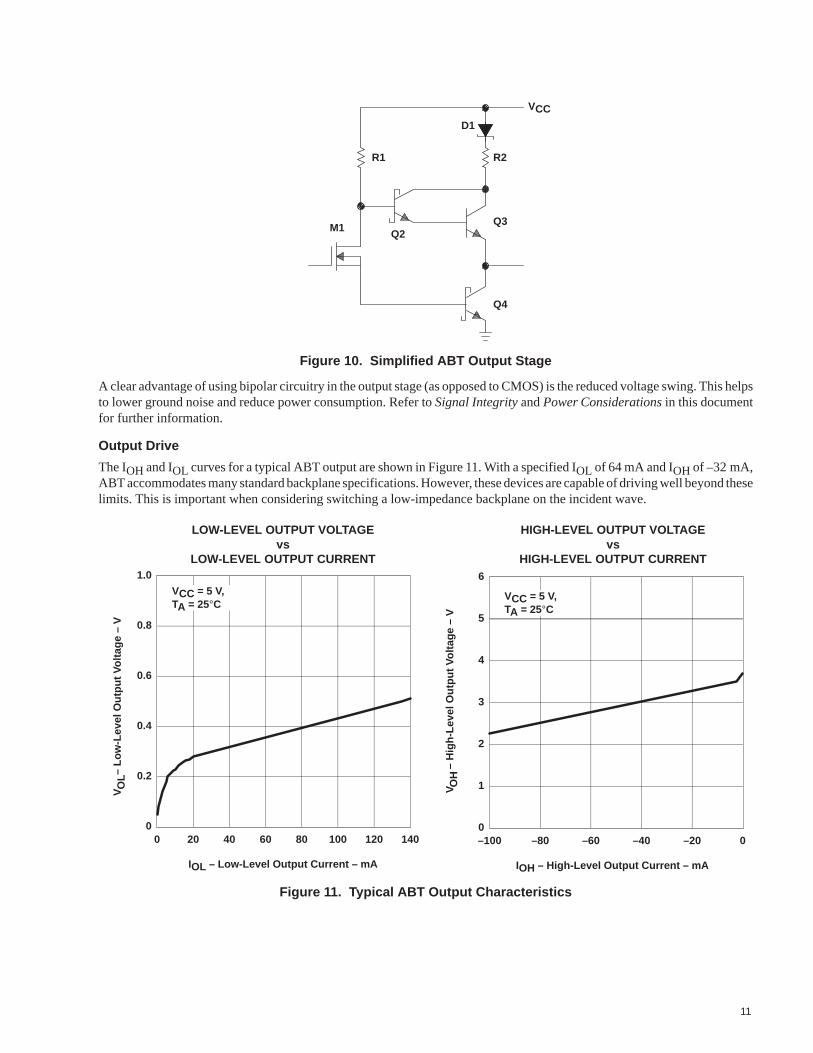
The current trend is consolidation of the functionality of multiple logic devices into complex, high pin-count ASICs andprogrammables. There are a number of important advantages for utilizing bus-interface devices in standard high-volumepackages. These include the need for high drive capability and good signal integrity. The use of bipolar circuitry in the outputstage makes it possible to provide these requirements, along with increased speed, using the ABT family.
Figure 10 shows a simplified schematic of an ABT output stage. Data is transmitted to the gate of M1, which acts as a simplecurrent switch. When M1 is turned on, current flows through R1 and M1 to the base of Q4, turning it on and driving the outputlow. At the same time, the base of Q2 is pulled low, thus turning off the upper output. For a low-to-high transition, the gateof M1 must be driven low, turning M1 off. Current through R1 charges the base of Q2, pulling it high and turning on theDarlington pair, consisting of Q2 and Q3. Meanwhile, with its supply of base drive cut off, Q4 turns off, and the output switchesfrom low to high. R2 is used to limit output current in the high state, and D1 is a blocking diode used to prevent reverse currentflow in specific power-down applications.
11
VCC
R1
D1
Q2
R2
Q3
Q4
M1
Figure 10. Simplified ABT Output Stage
A clear advantage of using bipolar circuitry in the output stage (as opposed to CMOS) is the reduced voltage swing. This helpsto lower ground noise and reduce power consumption. Refer to Signal Integrity and Power Considerations in this documentfor further information.
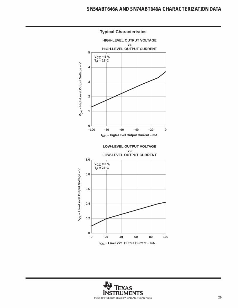
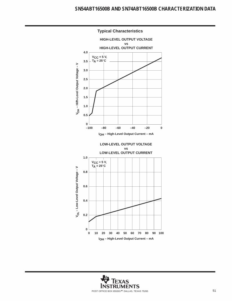
Output Drive
The IOH and IOL curves for a typical ABT output are shown in Figure 11. With a specified IOL of 64 mA and IOH of –32 mA,ABT accommodates many standard backplane specifications. However, these devices are capable of driving well beyond theselimits. This is important when considering switching a low-impedance backplane on the incident wave.
0
0.2
0.4
0.6
0.8
1.0
0 20 40 60 80 100 120 140
– L
ow-L
evel
Out
put V
olta
ge –
V
IOL – Low-Level Output Current – mA
LOW-LEVEL OUTPUT VOLTAGEvs
LOW-LEVEL OUTPUT CURRENT
0
1
2
3
4
5
6
–100 –80 –60 –40 –20 0
IOH – High-Level Output Current – mA
HIGH-LEVEL OUTPUT VOLTAGEvs
HIGH-LEVEL OUTPUT CURRENT
VO
L –
Hig
h-Le
vel O
utpu
t Vol
tage
– V
V OH
VCC = 5 V,TA = 25°C
VCC = 5 V,TA = 25°C
Figure 11. Typical ABT Output Characteristics
12
Incident-wave switching ensures that for a given transition (either high-to-low or low-to-high) the output reaches a valid VIHor VIL level on the initial wave front (i.e., does not require reflections). Figure 12 shows the problems a designer mightencounter when a device does not switch on the incident wave. A shelf below VIL(max), signal A, causes the propagation delayto slow by the amount of time it takes for the signal to reach the receiver and reflect back. Signal B shows the case in whichthere is a shelf in the threshold region. When this happens, the input to the receiver is uncertain and could cause severalproblems associated with slow input edges, depending on the length of time the shelf remains in this region. A signal as shownin example C does not cause a problem because the shelf does not occur until the necessary VIH level has been attained.
A B C
VIH(min)
VIL(max)
V
Figure 12. Reflected Wave Switching
Using typical VOH and VOL values along with data points from the curves, ABT devices can typically drive lines in the 25-Ωrange on the incident wave.
For a low-to-high transition, (IOH = 85 mA @ VOH = 2.4 V)
ZLH VOH(min) VOL(typ)
IOH
2.4 V 0.3 V85 mA
25
For a high-to-low transition, (IOL= 135 mA @ VOL= 0.5 V)
ZHL VOH(typ) VOL(max)
IOL
3.5 V 0.5 V135 mA
22
Partial Power Down
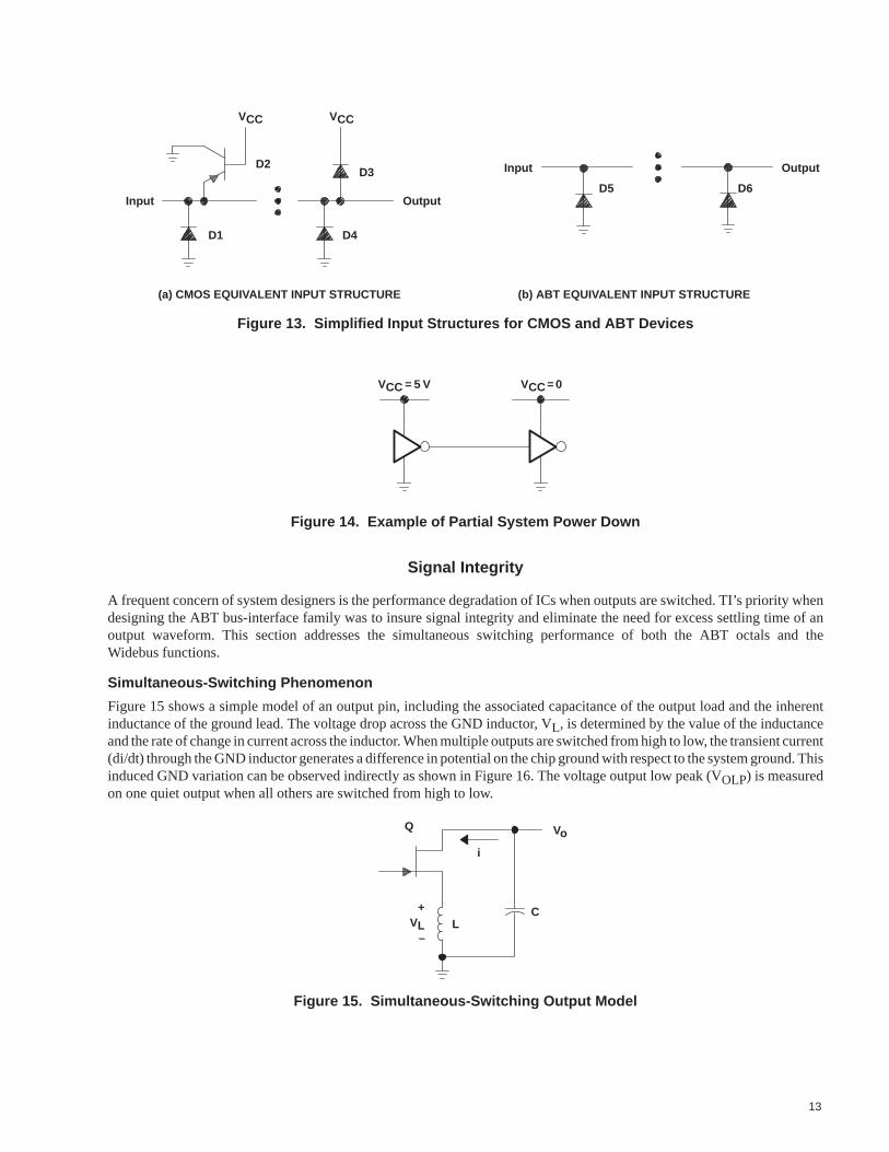
One application, addressed when designing the ABT family, is partial system power down. When using a standard CMOSdevice, there is a path from either the input or the output (or both) to VCC. This prevents partial power down for suchapplications as hot-card insertion without adding current limiting components. This is not the case with ABT as these pathshave been eliminated with the use of blocking diodes. Figure 13 shows functionally equivalent schematics of the inputstructures for CMOS and ABT devices.
Consider the situation shown in Figure 14. The driving device is powered with VCC = 5 V, while the receiving device is powereddown (VCC = 0). If these devices are CMOS, the receiver can be powered up through diode D2 when the driver is in a highstate. ABT devices do not have a comparable path and are thus immune to this problem, making them more desirable forthis application.
(1)
(2)
13
D5 D6
(a) CMOS EQUIVALENT INPUT STRUCTURE (b) ABT EQUIVALENT INPUT STRUCTURE
Input
VCC
D1
D2D3
D4
Output
Input Output
VCC
Figure 13. Simplified Input Structures for CMOS and ABT Devices
VCC = 5 V VCC = 0
Figure 14. Example of Partial System Power Down
Signal Integrity
A frequent concern of system designers is the performance degradation of ICs when outputs are switched. TI’s priority whendesigning the ABT bus-interface family was to insure signal integrity and eliminate the need for excess settling time of anoutput waveform. This section addresses the simultaneous switching performance of both the ABT octals and theWidebus functions.
Simultaneous-Switching Phenomenon
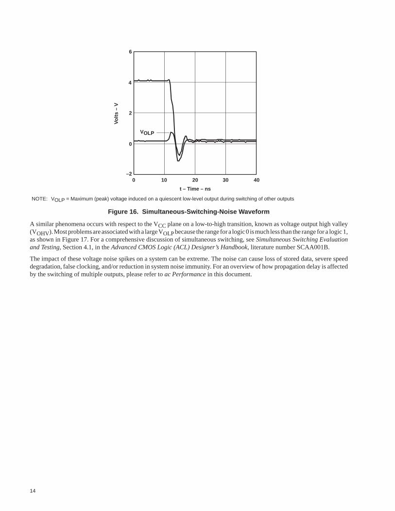
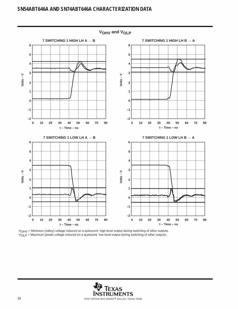
Figure 15 shows a simple model of an output pin, including the associated capacitance of the output load and the inherentinductance of the ground lead. The voltage drop across the GND inductor, VL, is determined by the value of the inductanceand the rate of change in current across the inductor. When multiple outputs are switched from high to low, the transient current(di/dt) through the GND inductor generates a difference in potential on the chip ground with respect to the system ground. Thisinduced GND variation can be observed indirectly as shown in Figure 16. The voltage output low peak (VOLP) is measuredon one quiet output when all others are switched from high to low.
Q
i
Vo
CLVL
+
–
Figure 15. Simultaneous-Switching Output Model
14
2
0
–2
6
4
0 10 20 30 40
Vol
ts –
V
VOLP
t – Time – ns
NOTE: VOLP = Maximum (peak) voltage induced on a quiescent low-level output during switching of other outputs
Figure 16. Simultaneous-Switching-Noise Waveform
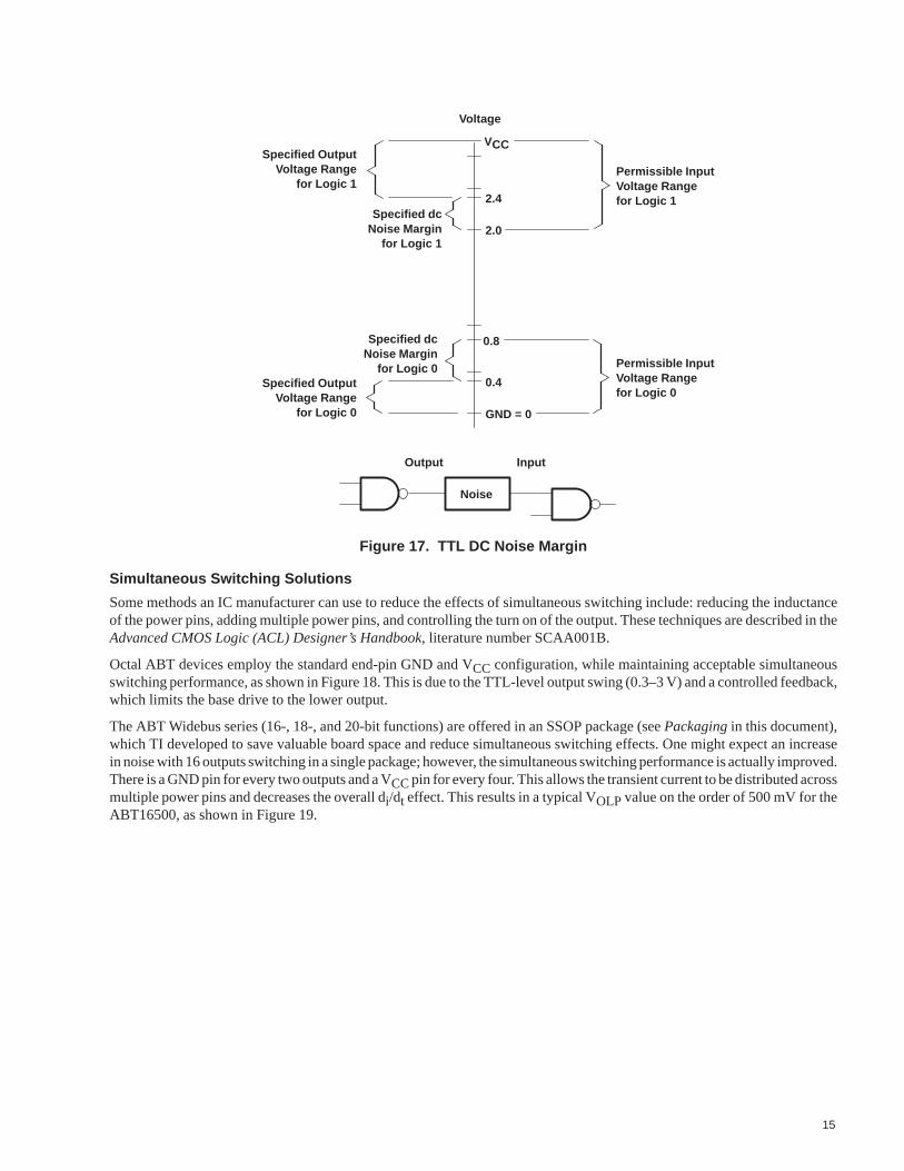
A similar phenomena occurs with respect to the VCC plane on a low-to-high transition, known as voltage output high valley(VOHV). Most problems are associated with a large VOLP because the range for a logic 0 is much less than the range for a logic 1,as shown in Figure 17. For a comprehensive discussion of simultaneous switching, see Simultaneous Switching Evaluationand Testing, Section 4.1, in the Advanced CMOS Logic (ACL) Designer’s Handbook, literature number SCAA001B.
The impact of these voltage noise spikes on a system can be extreme. The noise can cause loss of stored data, severe speeddegradation, false clocking, and/or reduction in system noise immunity. For an overview of how propagation delay is affectedby the switching of multiple outputs, please refer to ac Performance in this document.
15
0.4
0.8
2.0
2.4
GND = 0
Permissible InputVoltage Rangefor Logic 1
Specified OutputVoltage Range
for Logic 1
Specified dcNoise Margin
for Logic 1
Specified dcNoise Margin
for Logic 0Specified Output
Voltage Rangefor Logic 0
Voltage
Output Input
Permissible InputVoltage Rangefor Logic 0
Noise
VCC
Figure 17. TTL DC Noise Margin
Simultaneous Switching Solutions
Some methods an IC manufacturer can use to reduce the effects of simultaneous switching include: reducing the inductanceof the power pins, adding multiple power pins, and controlling the turn on of the output. These techniques are described in theAdvanced CMOS Logic (ACL) Designer’s Handbook, literature number SCAA001B.
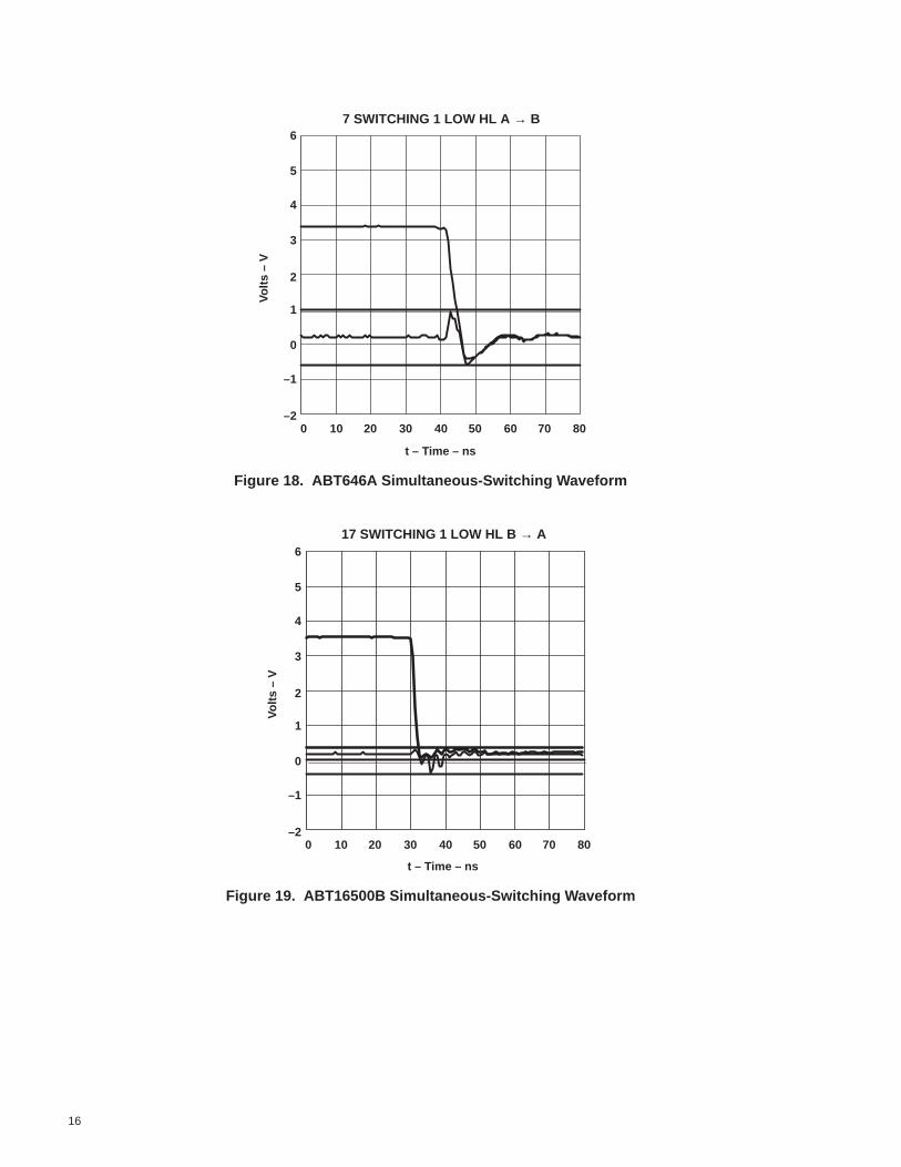
Octal ABT devices employ the standard end-pin GND and VCC configuration, while maintaining acceptable simultaneousswitching performance, as shown in Figure 18. This is due to the TTL-level output swing (0.3–3 V) and a controlled feedback,which limits the base drive to the lower output.
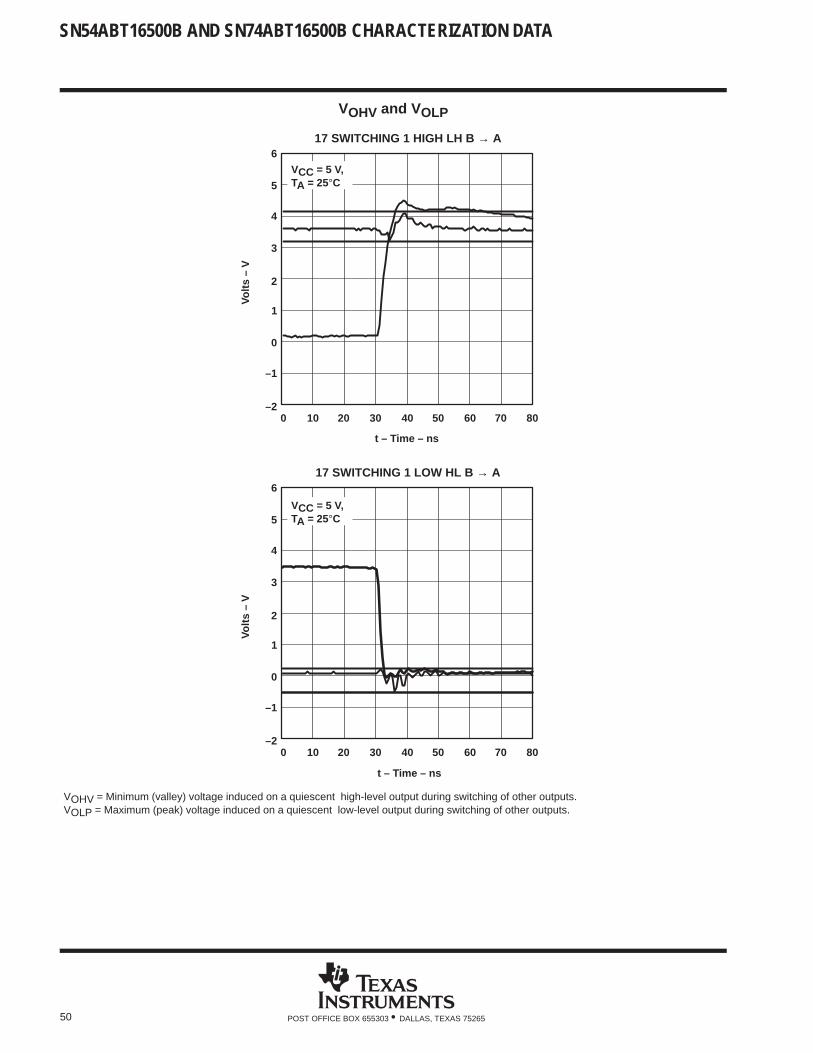
The ABT Widebus series (16-, 18-, and 20-bit functions) are offered in an SSOP package (see Packaging in this document),which TI developed to save valuable board space and reduce simultaneous switching effects. One might expect an increasein noise with 16 outputs switching in a single package; however, the simultaneous switching performance is actually improved.There is a GND pin for every two outputs and a VCC pin for every four. This allows the transient current to be distributed acrossmultiple power pins and decreases the overall di/dt effect. This results in a typical VOLP value on the order of 500 mV for theABT16500, as shown in Figure 19.
16
2
0
–1
–20 10 20 30 40 50
Vol
ts –
V
4
5
7 SWITCHING 1 LOW HL A → B6
60 70 80
3
1
t – Time – ns
Figure 18. ABT646A Simultaneous-Switching Waveform
2
0
–1
–20 10 20 30 40 50
Vol
ts –
V
4
5
17 SWITCHING 1 LOW HL B → A6
60 70 80
3
1
t – Time – ns
Figure 19. ABT16500B Simultaneous-Switching Waveform
17
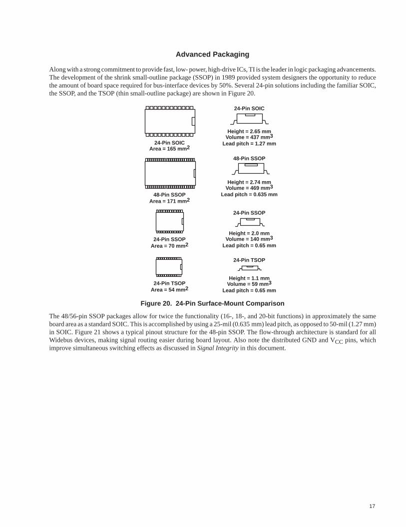
Advanced Packaging
Along with a strong commitment to provide fast, low- power, high-drive ICs, TI is the leader in logic packaging advancements.The development of the shrink small-outline package (SSOP) in 1989 provided system designers the opportunity to reducethe amount of board space required for bus-interface devices by 50%. Several 24-pin solutions including the familiar SOIC,the SSOP, and the TSOP (thin small-outline package) are shown in Figure 20.
24-Pin SOICArea = 165 mm 2
48-Pin SSOPArea = 171 mm 2
Height = 2.65 mm
24-Pin SSOPArea = 70 mm 2
24-Pin TSOPArea = 54 mm 2
24-Pin SOIC
48-Pin SSOP
24-Pin SSOP
24-Pin TSOP
Lead pitch = 1.27 mmVolume = 437 mm 3
Height = 2.74 mm
Lead pitch = 0.635 mmVolume = 469 mm 3
Height = 2.0 mm
Lead pitch = 0.65 mmVolume = 140 mm 3
Height = 1.1 mm
Lead pitch = 0.65 mmVolume = 59 mm 3
Figure 20. 24-Pin Surface-Mount Comparison
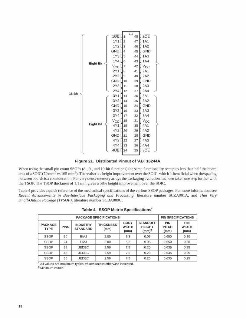
The 48/56-pin SSOP packages allow for twice the functionality (16-, 18-, and 20-bit functions) in approximately the sameboard area as a standard SOIC. This is accomplished by using a 25-mil (0.635 mm) lead pitch, as opposed to 50-mil (1.27 mm)in SOIC. Figure 21 shows a typical pinout structure for the 48-pin SSOP. The flow-through architecture is standard for allWidebus devices, making signal routing easier during board layout. Also note the distributed GND and VCC pins, whichimprove simultaneous switching effects as discussed in Signal Integrity in this document.
18
1
2
3
4
5
6
7
8
9
10
11
12
13
14
15
16
17
18
19
20
21
22
23
24
48
47
46
45
44
43
42
41
40
39
38
37
36
35
34
33
32
31
30
29
28
27
26
25
1OE1Y11Y2
GND1Y31Y4VCC2Y12Y2
GND2Y32Y43Y13Y2
GND3Y33Y4VCC4Y14Y2
GND4Y34Y44OE
2OE1A11A2GND1A31A4VCC2A12A2GND2A32A43A13A2GND3A33A4VCC4A14A2GND4A34A43OE
Eight Bit
Eight Bit
16 Bit
Figure 21. Distributed Pinout of ’ABT16244A
When using the small pin count SSOPs (8-, 9-, and 10-bit functions) the same functionality occupies less than half the boardarea of a SOIC (70 mm2 vs 165 mm2). There also is a height improvement over the SOIC, which is beneficial when the spacingbetween boards is a consideration. For very dense memory arrays the packaging evolution has been taken one step further withthe TSOP. The TSOP thickness of 1.1 mm gives a 58% height improvement over the SOIC.
Table 4 provides a quick reference of the mechanical specifications of the various SSOP packages. For more information, seeRecent Advancements in Bus-Interface Packaging and Processing, literature number SCZA001A, and Thin VerySmall-Outline Package (TVSOP), literature number SCBA009C.
Table 4. SSOP Metric Specifications †
PACKAGE SPECIFICATIONS PIN SPECIFICATIONS
PACKAGETYPE PINS
INDUSTRYSTANDARD
THICKNESS(mm)
BODYWIDTH(mm)
STANDOFFHEIGHT(mm)‡
PINPITCH(mm)
PINWIDTH(mm)
SSOP 20 EIAJ 2.00 5.3 0.05 0.650 0.30
SSOP 24 EIAJ 2.00 5.3 0.05 0.650 0.30
SSOP 28 JEDEC 2.59 7.5 0.20 0.635 0.25
SSOP 48 JEDEC 2.59 7.5 0.20 0.635 0.25
SSOP 56 JEDEC 2.59 7.5 0.20 0.635 0.25
† All values are maximum typical values unless otherwise indicated.‡ Minimum values
19POST OFFICE BOX 655303 • DALLAS, TEXAS 75265POST OFFICE BOX 1443 • HOUSTON, TEXAS 77251–1443
AAPPENDIX A’ABT646A Characterization Data

20 POST OFFICE BOX 655303 • DALLAS, TEXAS 75265POST OFFICE BOX 1443 • HOUSTON, TEXAS 77251–1443
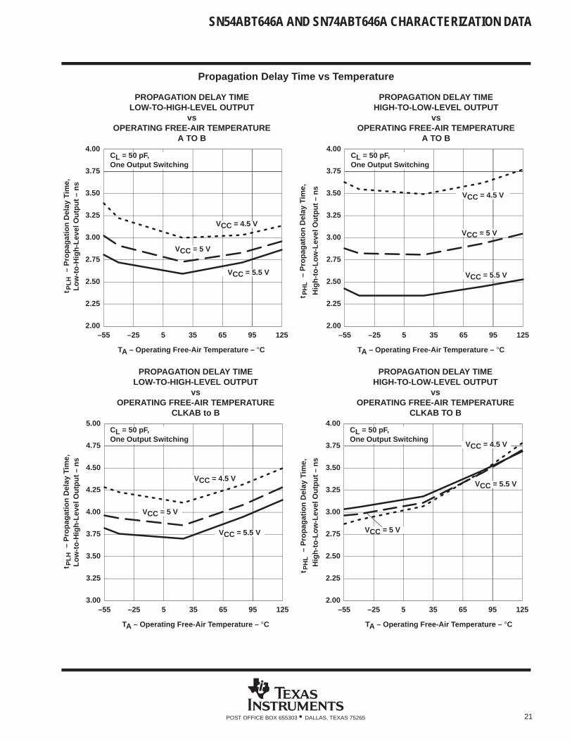
SN54ABT646A AND SN74ABT646A CHARACTERIZATION DATA
21POST OFFICE BOX 655303 • DALLAS, TEXAS 75265
Propagation Delay Time vs Temperature
2.00
2.25
2.50
2.75
3.00
3.25
3.50
3.75
4.00
–55 –25 5 35 65 95 1252.00
2.25
2.50
2.75
3.00
3.25
3.50
3.75
4.00
–55 –25 5 35 65 95 125
TA – Operating Free-Air Temperature – °C
PROPAGATION DELAY TIMELOW-TO-HIGH-LEVEL OUTPUT
vsOPERATING FREE-AIR TEMPERATURE
A TO B
VCC = 4.5 V
VCC = 5 V
VCC = 5.5 V
TA – Operating Free-Air Temperature – °C
PROPAGATION DELAY TIMEHIGH-TO-LOW-LEVEL OUTPUT
vsOPERATING FREE-AIR TEMPERATURE
A TO B
VCC = 4.5 V
VCC = 5 V
VCC = 5.5 V
3.00
3.25
3.50
3.75
4.00
4.25
4.50
4.75
5.00
–55 –25 5 35 65 95 125
TA – Operating Free-Air Temperature – °C
PROPAGATION DELAY TIMELOW-TO-HIGH-LEVEL OUTPUT
vsOPERATING FREE-AIR TEMPERATURE
CLKAB to B
VCC = 4.5 V
VCC = 5 V
VCC = 5.5 V
2.00
2.25
2.50
2.75
3.00
3.25
3.50
3.75
4.00
–55 –25 5 35 65 95 125
TA – Operating Free-Air Temperature – °C
PROPAGATION DELAY TIMEHIGH-TO-LOW-LEVEL OUTPUT
vsOPERATING FREE-AIR TEMPERATURE
CLKAB TO B
VCC = 4.5 V
VCC = 5 V
VCC = 5.5 V
t
–
Pro
paga
tion
Del
ay T
ime,
Low
-to-
Hig
h-Le
vel O
utpu
t – n
sP
LH
Hig
h-to
-Low
-Lev
el O
utpu
t – n
s
Low
-to-
Hig
h-Le
vel O
utpu
t – n
s
Hig
h-to
-Low
-Lev
el O
utpu
t – n
s
t
–
Pro
paga
tion
Del
ay T
ime,
PH
Lt
– P
ropa
gatio
n D
elay
Tim
e,P
HL
t
–
Pro
paga
tion
Del
ay T
ime,
PLH
CL = 50 pF,One Output Switching
CL = 50 pF,One Output Switching
CL = 50 pF,One Output Switching
CL = 50 pF,One Output Switching

SN54ABT646A AND SN74ABT646A CHARACTERIZATION DATA
22 POST OFFICE BOX 655303 • DALLAS, TEXAS 75265
Propagation Delay Time vs Temperature
3.0
3.3
3.6
3.9
4.2
4.5
4.8
5.1
5.4
5.7
6.0
–55 –25 5 35 65 95 125
TA – Operating Free-Air Temperature – °C
PROPAGATION DELAY TIMELOW-TO-HIGH-LEVEL OUTPUT
vsOPERATING FREE-AIR TEMPERATURE
SAB TO B
VCC = 4.5 V
VCC = 5 V
VCC = 5.5 V
2.0
2.3
2.6
2.9
3.2
3.5
3.8
4.1
4.4
4.7
5.0
–55 –25 5 35 65 95 125
PROPAGATION DELAY TIMEHIGH-TO-LOW-LEVEL OUTPUT
vsOPERATING FREE-AIR TEMPERATURE
SAB TO B
t
–
Pro
paga
tion
Del
ay T
ime,
Low
-to-
Hig
h-Le
vel O
utpu
t – n
sP
LHH
igh-
to-L
ow-L
evel
Out
put –
ns
TA – Operating Free-Air Temperature – °C
VCC = 4.5 V
VCC = 5 V
VCC = 5.5 V
t
–
Pro
paga
tion
Del
ay T
ime,
PH
LCL = 50 pF,One Output Switching
CL = 50 pF,One Output Switching
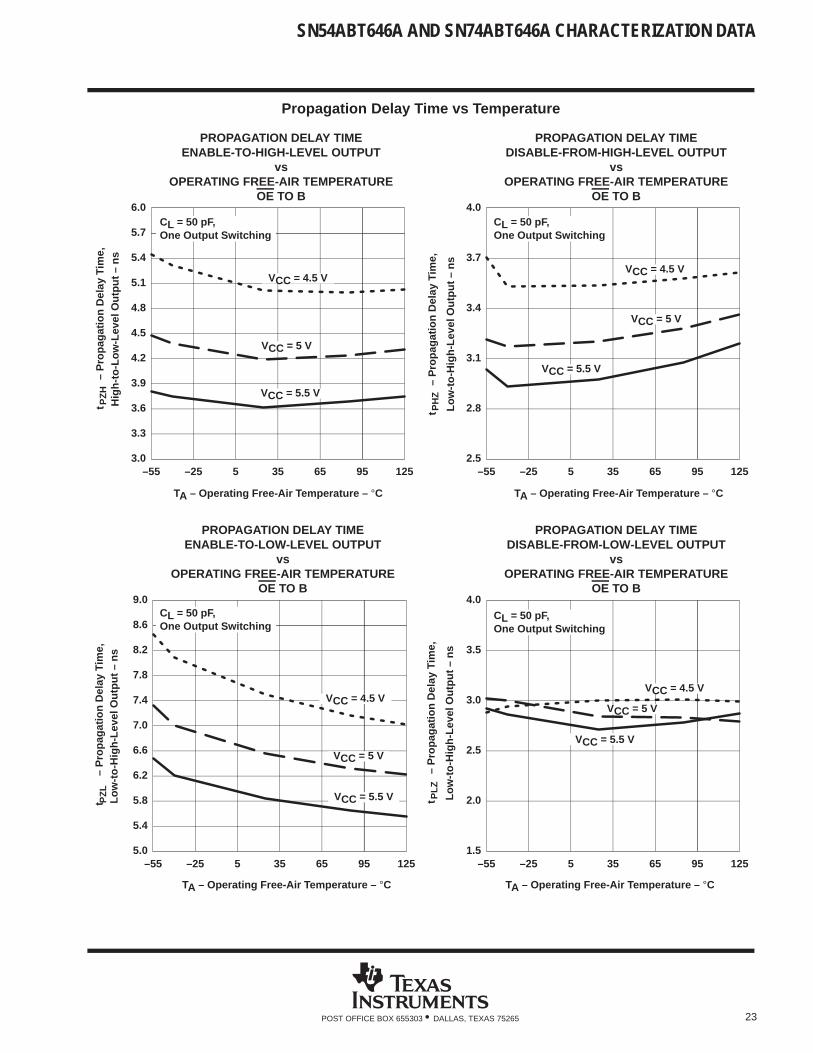
SN54ABT646A AND SN74ABT646A CHARACTERIZATION DATA
23POST OFFICE BOX 655303 • DALLAS, TEXAS 75265
Propagation Delay Time vs Temperature
3.0
3.3
3.6
3.9
4.2
4.5
4.8
5.1
5.4
5.7
6.0
–55 –25 5 35 65 95 125
PROPAGATION DELAY TIMEENABLE-TO-HIGH-LEVEL OUTPUT
vsOPERATING FREE-AIR TEMPERATURE
OE TO B
2.5
2.8
3.1
3.4
3.7
4.0
–55 –25 5 35 65 95 125
PROPAGATION DELAY TIMEDISABLE-FROM-HIGH-LEVEL OUTPUT
vsOPERATING FREE-AIR TEMPERATURE
OE TO B
5.0
5.4
5.8
6.2
6.6
7.0
7.4
7.8
8.2
8.6
9.0
–55 –25 5 35 65 95 125
TA – Operating Free-Air Temperature – °C
PROPAGATION DELAY TIMEENABLE-TO-LOW-LEVEL OUTPUT
vsOPERATING FREE-AIR TEMPERATURE
OE TO B
VCC = 4.5 V
VCC = 5 V
VCC = 5.5 V
1.5
2.0
2.5
3.0
3.5
4.0
–55 –25 5 35 65 95 125
TA – Operating Free-Air Temperature – °C
PROPAGATION DELAY TIMEDISABLE-FROM-LOW-LEVEL OUTPUT
vsOPERATING FREE-AIR TEMPERATURE
OE TO B
VCC = 4.5 V
VCC = 5 V
VCC = 5.5 V
Low
-to-
Hig
h-Le
vel O
utpu
t – n
s
t
–
Pro
paga
tion
Del
ay T
ime,
Hig
h-to
-Low
-Lev
el O
utpu
t – n
sP
ZH
Low
-to-
Hig
h-Le
vel O
utpu
t – n
s
Low
-to-
Hig
h-Le
vel O
utpu
t – n
s
TA – Operating Free-Air Temperature – °C
VCC = 4.5 V
VCC = 5 V
VCC = 5.5 V
VCC = 4.5 V
VCC = 5 V
VCC = 5.5 V
TA – Operating Free-Air Temperature – °C
t
–
Pro
paga
tion
Del
ay T
ime,
PH
Zt
– P
ropa
gatio
n D
elay
Tim
e,P
LZ
t
–
Pro
paga
tion
Del
ay T
ime,
PZ
L
CL = 50 pF,One Output Switching
CL = 50 pF,One Output Switching
CL = 50 pF,One Output Switching
CL = 50 pF,One Output Switching

SN54ABT646A AND SN74ABT646A CHARACTERIZATION DATA
24 POST OFFICE BOX 655303 • DALLAS, TEXAS 75265
Propagation Delay Time vs Temperature
4.5
4.8
5.1
5.4
5.7
6.0
–55 –25 5 35 65 95 125
TA – Operating Free-Air Temperature – °C
PROPAGATION DELAY TIMEENABLE-TO-HIGH-LEVEL OUTPUT
vsOPERATING FREE-AIR TEMPERATURE
DIR TO B
2.6
2.9
3.2
3.5
3.8
4.1
4.4
4.7
5.0
5.3
–55 –25 5 35 65 95 125
TA – Operating Free-Air Temperature – °C
PROPAGATION DELAY TIMEDISABLE-FROM-HIGH-LEVEL OUTPUT
vsOPERATING FREE-AIR TEMPERATURE
DIR TO B
4.5
4.8
5.1
5.4
5.7
6.0
6.3
6.6
6.9
7.2
–55 –25 5 35 65 95 125
TA – Operating Free-Air Temperature – °C
PROPAGATION DELAY TIMEENABLE-TO-LOW-LEVEL OUTPUT
vsOPERATING FREE-AIR TEMPERATURE
DIR TO B
2.5
2.8
3.1
3.4
3.7
4.0
4.3
4.6
4.9
–55 –25 5 35 65 95 125
TA – Operating Free-Air Temperature – °C
PROPAGATION DELAY TIMEDISABLE-FROM-LOW-LEVEL OUTPUT
vsOPERATING FREE-AIR TEMPERATURE
DIR TO B
Low
-to-
Hig
h-Le
vel O
utpu
t – n
s
Hig
h-to
-Low
-Lev
el O
utpu
t – n
sLo
w-t
o-H
igh-
Leve
l Out
put –
ns
Low
-to-
Hig
h-Le
vel O
utpu
t – n
s
t
–
Pro
paga
tion
Del
ay T
ime,
PZ
H
t
–
Pro
paga
tion
Del
ay T
ime,
PH
Zt
– P
ropa
gatio
n D
elay
Tim
e,
t
–
Pro
paga
tion
Del
ay T
ime,
PZ
L
CL = 50 pF,One Output Switching
CL = 50 pF,One Output Switching
CL = 50 pF,One Output Switching
CL = 50 pF,One Output Switching
VCC = 4.5 V
VCC = 5 V
VCC = 5.5 V
VCC = 4.5 V
VCC = 5 V
VCC = 5.5 V
VCC = 4.5 V
VCC = 5 V
VCC = 5.5 V
VCC = 4.5 V
VCC = 5 V
VCC = 5.5 V
PLZ
SN54ABT646A AND SN74ABT646A CHARACTERIZATION DATA
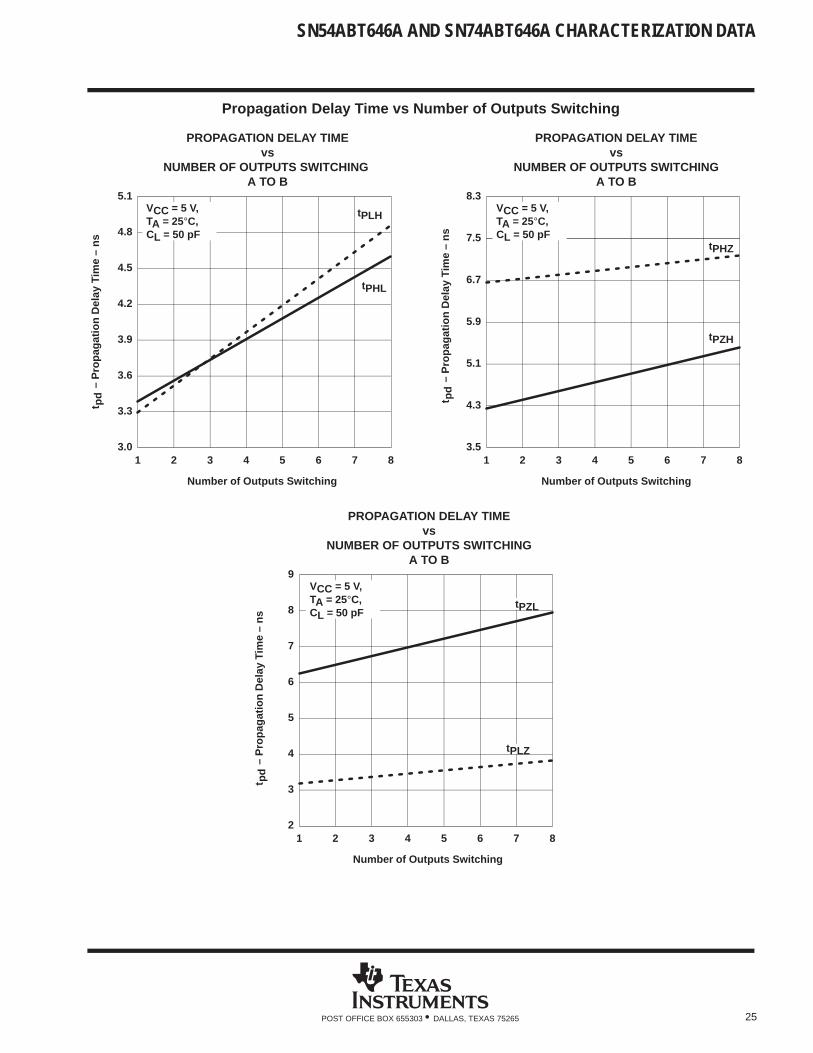
25POST OFFICE BOX 655303 • DALLAS, TEXAS 75265
Propagation Delay Time vs Number of Outputs Switching
2
3
4
5
6
7
8
9
1 2 3 4 5 6 7 8
3.0
3.3
3.6
3.9
4.2
4.5
4.8
5.1
1 2 3 4 5 6 7 8
Number of Outputs Switching
PROPAGATION DELAY TIMEvs
NUMBER OF OUTPUTS SWITCHING A TO B
3.5
4.3
5.1
5.9
6.7
7.5
8.3
1 2 3 4 5 6 7 8
Number of Outputs Switching
PROPAGATION DELAY TIMEvs
NUMBER OF OUTPUTS SWITCHINGA TO B
Number of Outputs Switching
PROPAGATION DELAY TIMEvs
NUMBER OF OUTPUTS SWITCHINGA TO B
tPLH
tPHL
tPHZ
tPZH
tPLZ
tPZL
VCC = 5 V,TA = 25°C,CL = 50 pF
t
– P
ropa
gatio
n D
elay
Tim
e –
nspd
t
– P
ropa
gatio
n D
elay
Tim
e –
nspd
t
– P
ropa
gatio
n D
elay
Tim
e –
nspd
VCC = 5 V,TA = 25°C,CL = 50 pF
VCC = 5 V,TA = 25°C,CL = 50 pF
SN54ABT646A AND SN74ABT646A CHARACTERIZATION DATA
26 POST OFFICE BOX 655303 • DALLAS, TEXAS 75265
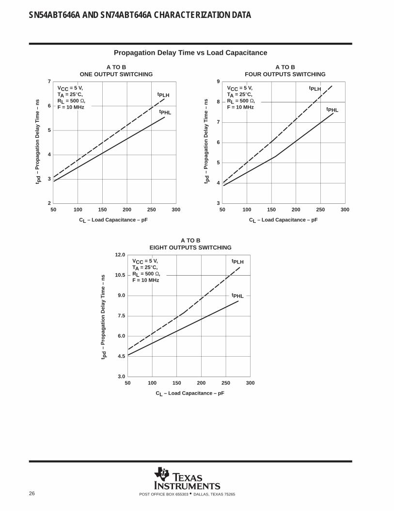
Propagation Delay Time vs Load Capacitance
2
3
4
5
6
7
50 100 150 200 250 3003
4
5
6
7
8
9
50 100 150 200 250 300
A TO BONE OUTPUT SWITCHING
A TO BFOUR OUTPUTS SWITCHING
3.0
4.5
6.0
7.5
9.0
10.5
12.0
50 100 150 200 250 300
A TO BEIGHT OUTPUTS SWITCHING
tPLH
tPHL
CL – Load Capacitance – pF
tPLH
tPHL
tPLH
tPHL
t
– P
ropa
gatio
n D
elay
Tim
e –
nspd t
– P
ropa
gatio
n D
elay
Tim
e –
nspd
t
– P
ropa
gatio
n D
elay
Tim
e –
nspd
CL – Load Capacitance – pF
CL – Load Capacitance – pF
VCC = 5 V,TA = 25°C,RL = 500 Ω,F = 10 MHz
VCC = 5 V,TA = 25°C,RL = 500 Ω,F = 10 MHz
VCC = 5 V,TA = 25°C,RL = 500 Ω,F = 10 MHz
SN54ABT646A AND SN74ABT646A CHARACTERIZATION DATA
27POST OFFICE BOX 655303 • DALLAS, TEXAS 75265
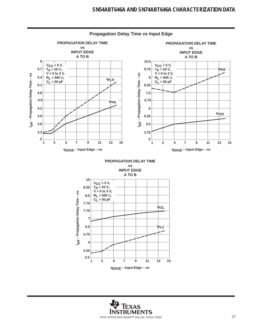
Propagation Delay Time vs Input Edge
tEDGE – Input Edge – ns
PROPAGATION DELAY TIMEvs
INPUT EDGEA TO B
PROPAGATION DELAY TIMEvs
INPUT EDGEA TO B
PROPAGATION DELAY TIMEvs
INPUT EDGEA TO B
tEDGE – Input Edge – ns
tEDGE – Input Edge – ns
4.75
3.25
8.5
2.51 3 5 7 9
5.5
7.75
10
11 13 15
9.25
7
4
3.9
3.3
5.4
31 3 5 7 9
4.8
4.2
5.1
6
11 13 15
5.7
4.5
3.6
5.25
3.75
9
31 3 5 7 9
7.5
6
8.25
10.5
11 13 15
9.75
6.75
4.5
tPLH
tPHL
tPZH
tPHZ
tPZL
tPLZ
t
– P
ropa
gatio
n D
elay
Tim
e –
nspd t
– P
ropa
gatio
n D
elay
Tim
e –
nspd
t
– P
ropa
gatio
n D
elay
Tim
e –
nspd
VCC = 5 V,TA = 25°C,V = 0 to 3 V,RL = 500 Ω,CL = 50 pF
7.75
VCC = 5 V,TA = 25°C,V = 0 to 3 V,RL = 500 Ω,CL = 50 pF
VCC = 5 V,TA = 25°C,V = 0 to 3 V,RL = 500 Ω,CL = 50 pF
SN54ABT646A AND SN74ABT646A CHARACTERIZATION DATA
28 POST OFFICE BOX 655303 • DALLAS, TEXAS 75265
VOHV and VOLP
2
0
–1
–20 10 20 30 40 50
Vol
ts –
V
4
5
7 SWITCHING 1 HIGH LH A → B6
60 70 80
3
1
2
0
–1
–20 10 20 30 40 50
Vol
ts –
V
4
5
7 SWITCHING 1 HIGH LH B → A6
60 70 80
3
1
2
0
–1
–20 10 20 30 40 50
Vol
ts –
V
4
5
7 SWITCHING 1 LOW LH A → B6
60 70 80
3
1
2
0
–1
–20 10 20 30 40 50
Vol
ts –
V
4
5
7 SWITCHING 1 LOW LH B → A6
60 70 80
3
1
t – Time – ns t – Time – ns
t – Time – nst – Time – ns
VOHV = Minimum (valley) voltage induced on a quiescent high-level output during switching of other outputs.VOLP = Maximum (peak) voltage induced on a quiescent low-level output during switching of other outputs.
SN54ABT646A AND SN74ABT646A CHARACTERIZATION DATA
29POST OFFICE BOX 655303 • DALLAS, TEXAS 75265
Typical Characteristics
0
1
2
3
4
5
–100 –80 –60 –40 –20 0
IOH – High-Level Output Current – mA
HIGH-LEVEL OUTPUT VOLTAGEvs
HIGH-LEVEL OUTPUT CURRENT
0
0.2
0.4
0.6
0.8
1.0
0 20 40 60 80 100
LOW-LEVEL OUTPUT VOLTAGEvs
LOW-LEVEL OUTPUT CURRENT
IOL – Low-Level Output Current – mA
–
Hig
h-Le
vel O
utpu
t Vol
tage
– V
V OH
– L
ow-L
evel
Out
put V
olta
ge –
VV
OL
VCC = 5 V,TA = 25°C
VCC = 5 V,TA = 25°C
SN54ABT646A AND SN74ABT646A CHARACTERIZATION DATA
30 POST OFFICE BOX 655303 • DALLAS, TEXAS 75265
Supply Current vs Frequency
0
5
10
15
20
25
30
35
40
45
50
0 10 20 30 40 50 60 70 80 90 100
F – Frequency – MHz
OUTPUTS ENABLED
0
0.5
1.0
1.5
2.0
2.5
3.0
3.5
0 10 20 30 40 50 60 70 80 90 100
F – Frequency – MHz
OUTPUTS DISABLED
– S
uppl
y C
urre
nt –
mA
CC
I
–
Sup
ply
Cur
rent
– m
AC
CI
VCC = 5 V,TA = 25°C,High Bias = 2.5 V,Low Bias = 0.5 V
VCC = 5 V,TA = 25°C,High Bias = 2.5 V,Low Bias = 0.5 V

31POST OFFICE BOX 655303 • DALLAS, TEXAS 75265POST OFFICE BOX 1443 • HOUSTON, TEXAS 77251–1443
BAPPENDIX BSN54ABT16244, SN74ABT16244ACharacterization Data

32 POST OFFICE BOX 655303 • DALLAS, TEXAS 75265POST OFFICE BOX 1443 • HOUSTON, TEXAS 77251–1443
SN54ABT16244 AND SN74ABT16244A CHARACTERIZATION DATA
33POST OFFICE BOX 655303 • DALLAS, TEXAS 75265
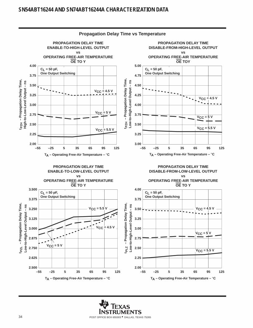
Propagation Delay Time vs Temperature
2.000
2.125
2.250
2.375
2.500
2.625
2.750
2.875
3.000
–55 –25 5 35 65 95 125
TA – Operating Free-Air Temperature – °C
PROPAGATION DELAY TIMELOW-TO-HIGH-LEVEL OUTPUT
vsOPERATING FREE-AIR TEMPERATURE
A TO Y
VCC = 4.5 V
VCC = 5 V
VCC = 5.5 V
1.00
1.25
1.50
1.75
2.00
2.25
2.50
2.75
3.00
–55 –25 5 35 65 95 125
TA – Operating Free-Air Temperature – °C
PROPAGATION DELAY TIMEHIGH-TO-LOW-LEVEL OUTPUT
vsOPERATING FREE-AIR TEMPERATURE
A TO Y
VCC = 4.5 V
VCC = 5 V
VCC = 5.5 V
t
–
Pro
paga
tion
Del
ay T
ime,
Low
-to-
Hig
h-Le
vel O
utpu
t – n
sP
LH
Hig
h-to
-Low
-Lev
el O
utpu
t – n
st
– P
ropa
gatio
n D
elay
Tim
e,P
HL
CL = 50 pF,One Output Switching
CL = 50 pF,One Output Switching
SN54ABT16244 AND SN74ABT16244A CHARACTERIZATION DATA
34 POST OFFICE BOX 655303 • DALLAS, TEXAS 75265
Propagation Delay Time vs Temperature
2.00
2.25
2.50
2.75
3.00
3.25
3.50
3.75
4.00
–55 –25 5 35 65 95 125
TA – Operating Free-Air Temperature – °C
PROPAGATION DELAY TIMEENABLE-TO-HIGH-LEVEL OUTPUT
vsOPERATING FREE-AIR TEMPERATURE
OE TO Y
3.00
3.25
3.50
3.75
4.00
4.25
4.50
4.75
5.00
–55 –25 5 35 65 95 125
PROPAGATION DELAY TIMEDISABLE-FROM-HIGH-LEVEL OUTPUT
vsOPERATING FREE-AIR TEMPERATURE
OE TOY
2.500
2.625
2.750
2.875
3.000
3.125
3.250
3.375
3.500
–55 –25 5 35 65 95 125
PROPAGATION DELAY TIMEENABLE-TO-LOW-LEVEL OUTPUT
vsOPERATING FREE-AIR TEMPERATURE
OE TO Y
2.00
2.25
2.50
2.75
3.00
3.25
3.50
3.75
4.00
–55 –25 5 35 65 95 125
PROPAGATION DELAY TIMEDISABLE-FROM-LOW-LEVEL OUTPUT
vsOPERATING FREE-AIR TEMPERATURE
OE TO Y
Low
-to-
Hig
h-Le
vel O
utpu
t – n
s
t
–
Pro
paga
tion
Del
ay T
ime,
Hig
h-to
-Low
-Lev
el O
utpu
t – n
sP
ZH
Low
-to-
Hig
h-Le
vel O
utpu
t – n
s
Low
-to-
Hig
h-Le
vel O
utpu
t – n
s
TA – Operating Free-Air Temperature – °C
TA – Operating Free-Air Temperature – °C TA – Operating Free-Air Temperature – °C
t
–
Pro
paga
tion
Del
ay T
ime,
PZ
Ht
– P
ropa
gatio
n D
elay
Tim
e,P
LZ
t
–
Pro
paga
tion
Del
ay T
ime,
PZ
L
CL = 50 pF,One Output Switching
VCC = 4.5 V
VCC = 5 V
VCC = 5.5 V
VCC = 4.5 V
VCC = 5 V
VCC = 5.5 V
VCC = 4.5 V
VCC = 5 V
VCC = 5.5 V VCC = 4.5 V
VCC = 5 V
VCC = 5.5 V
CL = 50 pF,One Output Switching
CL = 50 pF,One Output Switching
CL = 50 pF,One Output Switching

SN54ABT16244 AND SN74ABT16244A CHARACTERIZATION DATA
35POST OFFICE BOX 655303 • DALLAS, TEXAS 75265
Propagation Delay Time vs Number of Outputs Switching
2.00
2.50
3.00
3.50
4.00
1 4 7 10 13 16
2.00
2.25
2.50
2.75
3.00
1 4 7 10 13 16
Number of Outputs Switching
PROPAGATION DELAY TIMEvs
NUMBER OF OUTPUTS SWITCHING A TO Y
3.00
3.25
3.50
3.75
4.00
1 4 7 10 13 16
Number of Outputs Switching
PROPAGATION DELAY TIMEvs
NUMBER OF OUTPUTS SWITCHINGOE TO Y
Number of Outputs Switching
PROPAGATION DELAY TIMEvs
NUMBER OF OUTPUTS SWITCHINGOE TO Y
tPLHtPHL
tPHZ
tPZH
tPLZ
tPZL
t
– P
ropa
gatio
n D
elay
Tim
e –
nspd t
– P
ropa
gatio
n D
elay
Tim
e –
nspd
t
– P
ropa
gatio
n D
elay
Tim
e –
nspd
VCC = 5 V,TA = 25°C,CL = 50 pF
VCC = 5 V,TA = 25°C,CL = 50 pF
VCC = 5 V,TA = 25°C,CL = 50 pF

SN54ABT16244 AND SN74ABT16244A CHARACTERIZATION DATA
36 POST OFFICE BOX 655303 • DALLAS, TEXAS 75265
Propagation Delay Time vs Load Capacitance
2.00
2.50
3.00
3.50
4.00
4.50
5.00
50 100 150 200 250 3002.0
2.5
3.0
3.5
4.0
4.5
5.0
5.5
6.0
50 100 150 200 250 300
A TO YONE OUTPUT SWITCHING
A TO YFOUR OUTPUTS SWITCHING
2.0
2.5
3.0
3.5
4.0
4.5
5.0
5.5
6.0
50 100 150 200 250 300
A TO YEIGHT OUTPUTS SWITCHING
tPLH
tPHL
CL – Load Capacitance – pF
CL – Load Capacitance – pFCL – Load Capacitance – pF
tPHL
tPLH
tPLH
tPHL
2.0
2.5
3.0
3.5
4.0
4.5
5.0
5.5
6.0
50 100 150 200 250 300
A TO Y16 OUTPUTS SWITCHING
tPLH
tPHL
CL – Load Capacitance – pF
t
– P
ropa
gatio
n D
elay
Tim
e –
nspd t
– P
ropa
gatio
n D
elay
Tim
e –
nspd
t
– P
ropa
gatio
n D
elay
Tim
e –
nspdt
–
Pro
paga
tion
Del
ay T
ime
– ns
pd
VCC = 5 V,TA = 25°C,RL = 500 Ω,F = 10 MHz
VCC = 5 V,TA = 25°C,RL = 500 Ω,F = 10 MHz
VCC = 5 V,TA = 25°C,RL = 500 Ω,F = 10 MHz
VCC = 5 V,TA = 25°C,RL = 500 Ω,F = 10 MHz
SN54ABT16244 AND SN74ABT16244A CHARACTERIZATION DATA
37POST OFFICE BOX 655303 • DALLAS, TEXAS 75265
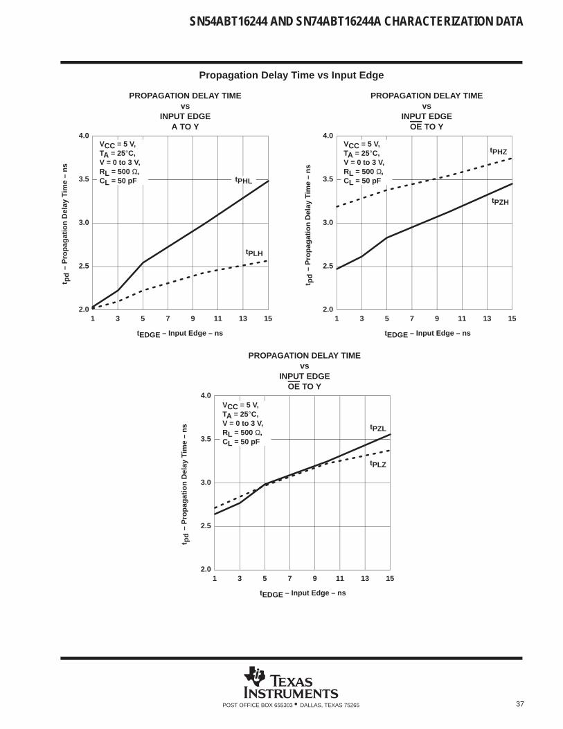
Propagation Delay Time vs Input Edge
2.0
2.5
3.0
3.5
4.0
1 3 5 7 9 11 13 15
2.0
2.5
3.0
3.5
4.0
1 3 5 7 9 11 13 15
tEDGE – Input Edge – ns
PROPAGATION DELAY TIMEvs
INPUT EDGEA TO Y
2.0
2.5
3.0
3.5
4.0
1 3 5 7 9 11 13 15
PROPAGATION DELAY TIMEvs
INPUT EDGEOE TO Y
PROPAGATION DELAY TIMEvs
INPUT EDGEOE TO Y
tPLH
tPHL
tEDGE – Input Edge – ns
tEDGE – Input Edge – ns
tPZL
tPLZ
tPHZ
tPZH
t
– P
ropa
gatio
n D
elay
Tim
e –
nspd t
– P
ropa
gatio
n D
elay
Tim
e –
nspd
t
– P
ropa
gatio
n D
elay
Tim
e –
nspd
VCC = 5 V,TA = 25°C,V = 0 to 3 V,RL = 500 Ω,CL = 50 pF
VCC = 5 V,TA = 25°C,V = 0 to 3 V,RL = 500 Ω,CL = 50 pF
VCC = 5 V,TA = 25°C,V = 0 to 3 V,RL = 500 Ω,CL = 50 pF

SN54ABT16244 AND SN74ABT16244A CHARACTERIZATION DATA
38 POST OFFICE BOX 655303 • DALLAS, TEXAS 75265
VOHV and VOLP
2
0
–1
–20 10 20 30 40 50
Vol
ts –
V
4
5
15 SWITCHING 1 HIGH LH A → Y6
60 70 80
3
1
2
0
–1
–20 10 20 30 40 50
Vol
ts –
V
4.
5
6
60 70 80
3
1
15 SWITCHING 1 LOW HL A → Y
t – Time – ns
t – Time – ns
VCC = 5 V,TA = 25°C
VCC = 5 V,TA = 25°C
VOHV = Minimum (valley) voltage induced on a quiescent high-level output during switching of other outputs.VOLP = Maximum (peak) voltage induced on a quiescent low-level output during switching of other outputs.
SN54ABT16244 AND SN74ABT16244A CHARACTERIZATION DATA
39POST OFFICE BOX 655303 • DALLAS, TEXAS 75265
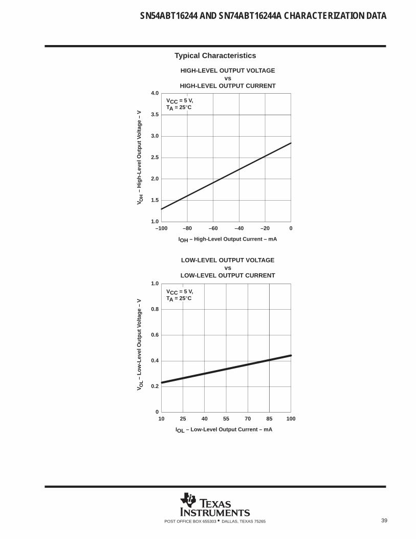
Typical Characteristics
1.0
1.5
2.0
2.5
3.0
3.5
4.0
–100 –80 –60 –40 –20 0
IOH – High-Level Output Current – mA
HIGH-LEVEL OUTPUT VOLTAGEvs
HIGH-LEVEL OUTPUT CURRENT
0
0.2
0.4
0.6
0.8
1.0
10 25 40 55 70 85 100
LOW-LEVEL OUTPUT VOLTAGEvs
LOW-LEVEL OUTPUT CURRENT
IOL – Low-Level Output Current – mA
–
Hig
h-Le
vel O
utpu
t Vol
tage
– V
V OH
– L
ow-L
evel
Out
put V
olta
ge –
VV
OL
VCC = 5 V,TA = 25°C
VCC = 5 V,TA = 25°C
SN54ABT16244 AND SN74ABT16244A CHARACTERIZATION DATA
40 POST OFFICE BOX 655303 • DALLAS, TEXAS 75265
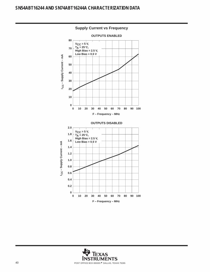
Supply Current vs Frequency
0
10
20
30
40
50
60
70
80
0 10 20 30 40 50 60 70 80 90 100
F – Frequency – MHz
OUTPUTS ENABLED
0
0.2
0.4
0.6
0.8
1.0
1.2
1.4
1.6
1.8
2.0
0 10 20 30 40 50 60 70 80 90 100
F – Frequency – MHz
OUTPUTS DISABLED
– S
uppl
y C
urre
nt –
mA
CC
I
–
Sup
ply
Cur
rent
– m
AC
CI
VCC = 5 V,TA = 25°C,High Bias = 2.5 V,Low Bias = 0.5 V
VCC = 5 V,TA = 25°C,High Bias = 2.5 V,Low Bias = 0.5 V
41POST OFFICE BOX 655303 • DALLAS, TEXAS 75265POST OFFICE BOX 1443 • HOUSTON, TEXAS 77251–1443
CAPPENDIX C’ABT16500B Characterization Data

42 POST OFFICE BOX 655303 • DALLAS, TEXAS 75265POST OFFICE BOX 1443 • HOUSTON, TEXAS 77251–1443
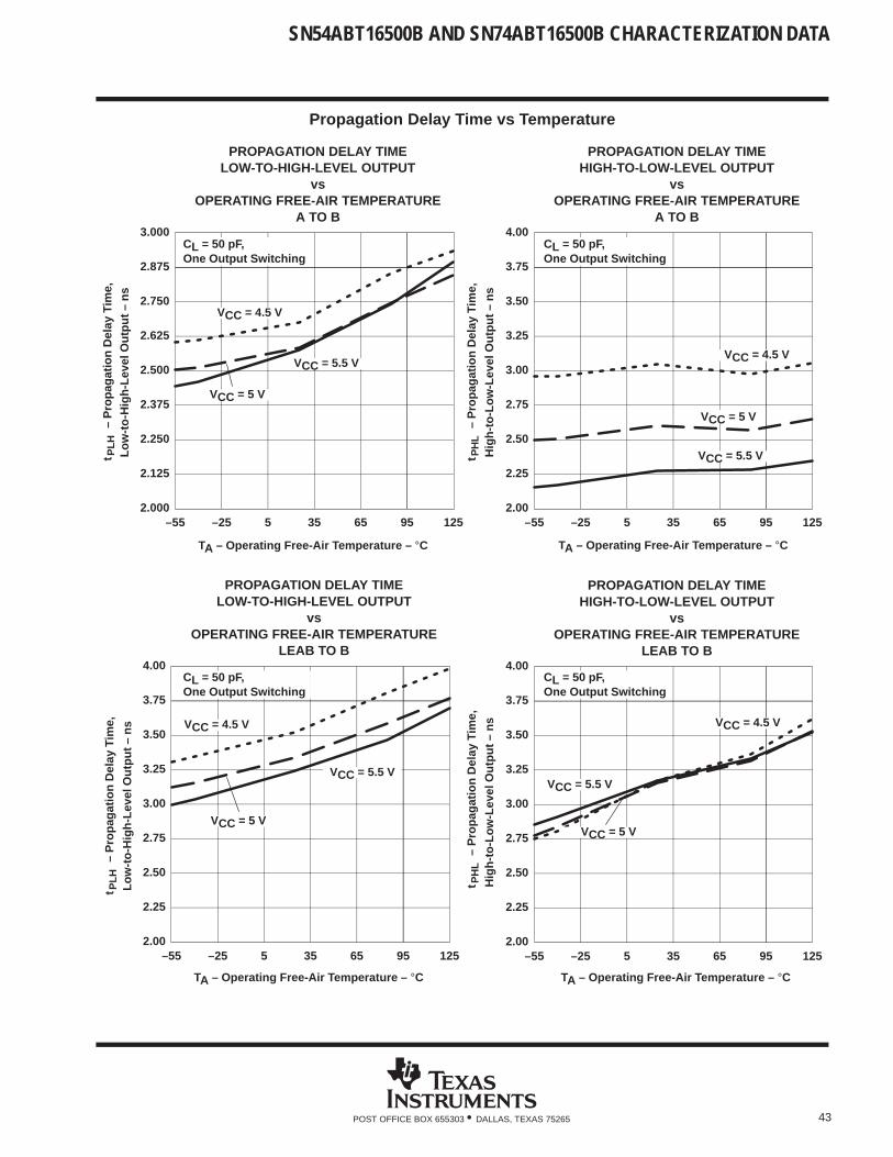
SN54ABT16500B AND SN74ABT16500B CHARACTERIZATION DATA
43POST OFFICE BOX 655303 • DALLAS, TEXAS 75265
Propagation Delay Time vs Temperature
2.000
2.125
2.250
2.375
2.500
2.625
2.750
2.875
3.000
–55 –25 5 35 65 95 125
TA – Operating Free-Air Temperature – °C
PROPAGATION DELAY TIMELOW-TO-HIGH-LEVEL OUTPUT
vsOPERATING FREE-AIR TEMPERATURE
A TO B
VCC = 4.5 V
VCC = 5 V
VCC = 5.5 V
2.00
2.25
2.50
2.75
3.00
3.25
3.50
3.75
4.00
–55 –25 5 35 65 95 125
PROPAGATION DELAY TIMELOW-TO-HIGH-LEVEL OUTPUT
vsOPERATING FREE-AIR TEMPERATURE
LEAB TO B
2.00
2.25
2.50
2.75
3.00
3.25
3.50
3.75
4.00
–55 –25 5 35 65 95 125
PROPAGATION DELAY TIMEHIGH-TO-LOW-LEVEL OUTPUT
vsOPERATING FREE-AIR TEMPERATURE
A TO B
2.00
2.25
2.50
2.75
3.00
3.25
3.50
3.75
4.00
–55 –25 5 35 65 95 125
PROPAGATION DELAY TIMEHIGH-TO-LOW-LEVEL OUTPUT
vsOPERATING FREE-AIR TEMPERATURE
LEAB TO B
t
–
Pro
paga
tion
Del
ay T
ime,
Low
-to-
Hig
h-Le
vel O
utpu
t – n
sP
LH
Hig
h-to
-Low
-Lev
el O
utpu
t – n
s
Low
-to-
Hig
h-Le
vel O
utpu
t – n
s
Hig
h-to
-Low
-Lev
el O
utpu
t – n
s
TA – Operating Free-Air Temperature – °C
VCC = 4.5 V
VCC = 5 V
VCC = 5.5 V
TA – Operating Free-Air Temperature – °C
VCC = 4.5 V
VCC = 5 V
VCC = 5.5 V
TA – Operating Free-Air Temperature – °C
VCC = 4.5 V
VCC = 5 V
VCC = 5.5 V
t
–
Pro
paga
tion
Del
ay T
ime,
PH
Lt
– P
ropa
gatio
n D
elay
Tim
e,P
HL
t
–
Pro
paga
tion
Del
ay T
ime,
PLH
CL = 50 pF,One Output Switching
CL = 50 pF,One Output Switching
CL = 50 pF,One Output Switching
CL = 50 pF,One Output Switching
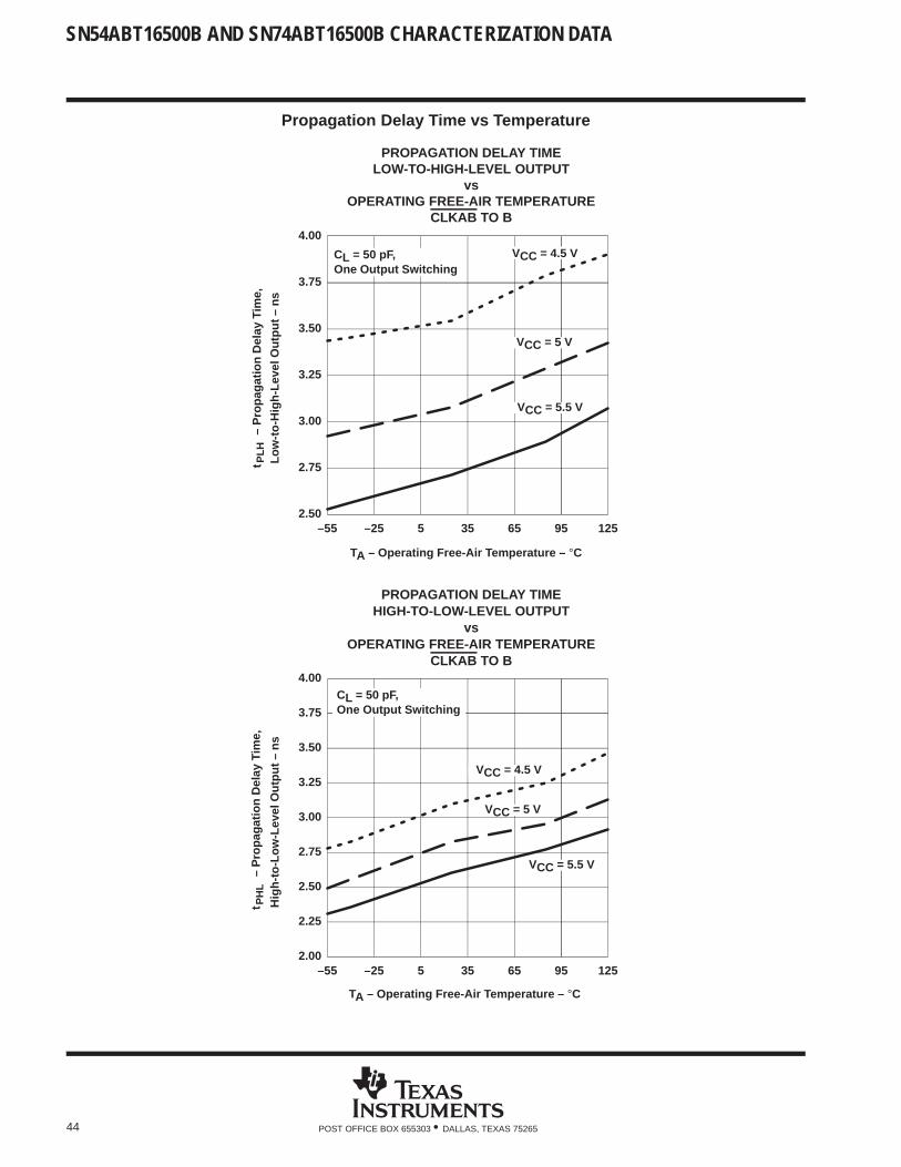
SN54ABT16500B AND SN74ABT16500B CHARACTERIZATION DATA
44 POST OFFICE BOX 655303 • DALLAS, TEXAS 75265
Propagation Delay Time vs Temperature
2.50
2.75
3.00
3.25
3.50
3.75
4.00
–55 –25 5 35 65 95 125
PROPAGATION DELAY TIMELOW-TO-HIGH-LEVEL OUTPUT
vsOPERATING FREE-AIR TEMPERATURE
CLKAB TO B
2.00
2.25
2.50
2.75
3.00
3.25
3.50
3.75
4.00
–55 –25 5 35 65 95 125
PROPAGATION DELAY TIMEHIGH-TO-LOW-LEVEL OUTPUT
vsOPERATING FREE-AIR TEMPERATURE
CLKAB TO B
Low
-to-
Hig
h-Le
vel O
utpu
t – n
sH
igh-
to-L
ow-L
evel
Out
put –
ns
TA – Operating Free-Air Temperature – °C
VCC = 4.5 V
VCC = 5 V
VCC = 5.5 V
TA – Operating Free-Air Temperature – °C
VCC = 4.5 V
VCC = 5 V
VCC = 5.5 V
t
–
Pro
paga
tion
Del
ay T
ime,
PLH
t
–
Pro
paga
tion
Del
ay T
ime,
PH
LCL = 50 pF,One Output Switching
CL = 50 pF,One Output Switching
SN54ABT16500B AND SN74ABT16500B CHARACTERIZATION DATA
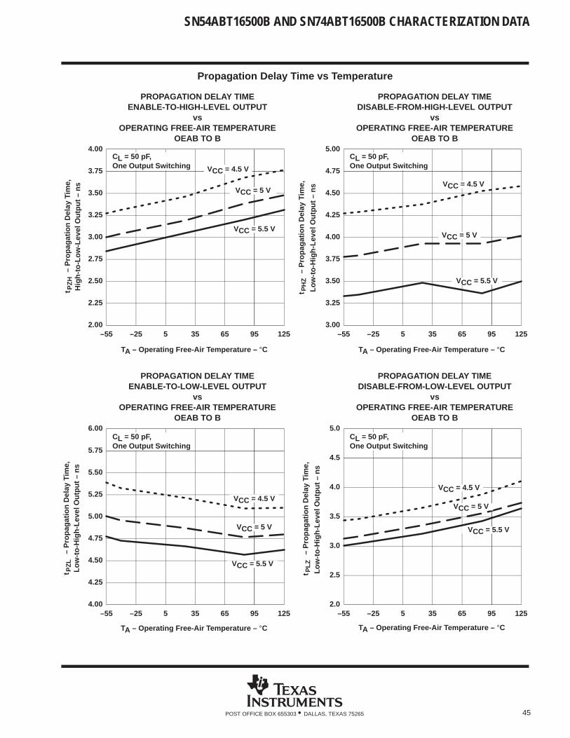
45POST OFFICE BOX 655303 • DALLAS, TEXAS 75265
Propagation Delay Time vs Temperature
2.00
2.25
2.50
2.75
3.00
3.25
3.50
3.75
4.00
–55 –25 5 35 65 95 125
PROPAGATION DELAY TIMEENABLE-TO-HIGH-LEVEL OUTPUT
vsOPERATING FREE-AIR TEMPERATURE
OEAB TO B
3.00
3.25
3.50
3.75
4.00
4.25
4.50
4.75
5.00
–55 –25 5 35 65 95 125
PROPAGATION DELAY TIMEDISABLE-FROM-HIGH-LEVEL OUTPUT
vsOPERATING FREE-AIR TEMPERATURE
OEAB TO B
4.00
4.25
4.50
4.75
5.00
5.25
5.50
5.75
6.00
–55 –25 5 35 65 95 125
PROPAGATION DELAY TIMEENABLE-TO-LOW-LEVEL OUTPUT
vsOPERATING FREE-AIR TEMPERATURE
OEAB TO B
2.0
2.5
3.0
3.5
4.0
4.5
5.0
–55 –25 5 35 65 95 125
PROPAGATION DELAY TIMEDISABLE-FROM-LOW-LEVEL OUTPUT
vsOPERATING FREE-AIR TEMPERATURE
OEAB TO B
Low
-to-
Hig
h-Le
vel O
utpu
t – n
s
t
–
Pro
paga
tion
Del
ay T
ime,
Hig
h-to
-Low
-Lev
el O
utpu
t – n
sP
ZH
Low
-to-
Hig
h-Le
vel O
utpu
t – n
s
Low
-to-
Hig
h-Le
vel O
utpu
t – n
s
TA – Operating Free-Air Temperature – °C
VCC = 4.5 V
VCC = 5 V
VCC = 5.5 V
TA – Operating Free-Air Temperature – °C
VCC = 4.5 V
VCC = 5 V
VCC = 5.5 V
TA – Operating Free-Air Temperature – °C
VCC = 4.5 V
VCC = 5 V
VCC = 5.5 V
TA – Operating Free-Air Temperature – °C
VCC = 4.5 V
VCC = 5 V
VCC = 5.5 V
t
–
Pro
paga
tion
Del
ay T
ime,
PH
Z
t
–
Pro
paga
tion
Del
ay T
ime,
PZ
L
t
–
Pro
paga
tion
Del
ay T
ime,
PLZ
CL = 50 pF,One Output Switching
CL = 50 pF,One Output Switching
CL = 50 pF,One Output Switching
CL = 50 pF,One Output Switching
SN54ABT16500B AND SN74ABT16500B CHARACTERIZATION DATA
46 POST OFFICE BOX 655303 • DALLAS, TEXAS 75265
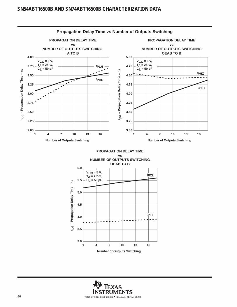
Propagation Delay Time vs Number of Outputs Switching
3.0
3.5
4.0
4.5
5.0
5.5
6.0
1 4 7 10 13 16
2.00
2.25
2.50
2.75
3.00
3.25
3.50
3.75
4.00
1 4 7 10 13 16
Number of Outputs Switching
PROPAGATION DELAY TIMEvs
NUMBER OF OUTPUTS SWITCHING A TO B
3.00
3.25
3.50
3.75
4.00
4.25
4.50
4.75
5.00
1 4 7 10 13 16
Number of Outputs Switching
PROPAGATION DELAY TIMEvs
NUMBER OF OUTPUTS SWITCHINGOEAB TO B
Number of Outputs Switching
PROPAGATION DELAY TIMEvs
NUMBER OF OUTPUTS SWITCHINGOEAB TO B
tPLH
tPHL
tPHZ
tPZH
tPLZ
tPZL
t
– P
ropa
gatio
n D
elay
Tim
e –
nspd t
– P
ropa
gatio
n D
elay
Tim
e –
nspd
t
– P
ropa
gatio
n D
elay
Tim
e –
nspd
VCC = 5 V,TA = 25°C,CL = 50 pF
VCC = 5 V,TA = 25°C,CL = 50 pF
VCC = 5 V,TA = 25°C,CL = 50 pF
SN54ABT16500B AND SN74ABT16500B CHARACTERIZATION DATA
47POST OFFICE BOX 655303 • DALLAS, TEXAS 75265
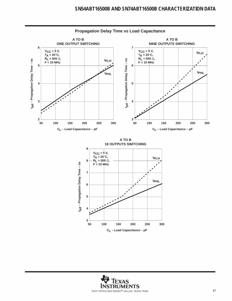
Propagation Delay Time vs Load Capacitance
2
3
4
5
6
50 100 150 200 250 3003
4
5
6
7
50 100 150 200 250 300
A TO BONE OUTPUT SWITCHING
A TO BNINE OUTPUTS SWITCHING
3
4
5
6
7
8
9
50 100 150 200 250 300
A TO B18 OUTPUTS SWITCHING
tPLH
tPHL
CL – Load Capacitance – pF
CL – Load Capacitance – pFCL – Load Capacitance – pF
tPHL
tPLH
tPLH
tPHL
t
– P
ropa
gatio
n D
elay
Tim
e –
nspd t
–
Pro
paga
tion
Del
ay T
ime
– ns
pd
t
– P
ropa
gatio
n D
elay
Tim
e –
nspd
VCC = 5 V,TA = 25°C,RL = 500 Ω,F = 10 MHz
VCC = 5 V,TA = 25°C,RL = 500 Ω,F = 10 MHz
VCC = 5 V,TA = 25°C,RL = 500 Ω,F = 10 MHz
SN54ABT16500B AND SN74ABT16500B CHARACTERIZATION DATA
48 POST OFFICE BOX 655303 • DALLAS, TEXAS 75265
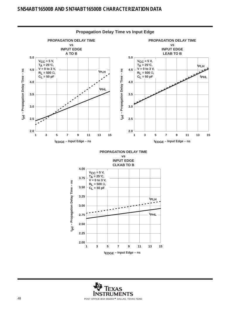
Propagation Delay Time vs Input Edge
tPHL
2.00
2.25
2.50
2.75
3.00
3.25
3.50
3.75
4.00
1 3 5 7 9 11 13 15
2.0
2.5
3.0
3.5
4.0
4.5
5.0
1 3 5 7 9 11 13 15
tEDGE – Input Edge – ns
PROPAGATION DELAY TIMEvs
INPUT EDGEA TO B
2.0
2.5
3.0
3.5
4.0
4.5
5.0
1 3 5 7 9 11 13 15
PROPAGATION DELAY TIMEvs
INPUT EDGELEAB TO B
PROPAGATION DELAY TIMEvs
INPUT EDGECLKAB TO B
tPLH
tPHL
tEDGE – Input Edge – ns
tEDGE – Input Edge – ns
tPLH
tPHL
tPLH
t
– P
ropa
gatio
n D
elay
Tim
e –
nspd t
– P
ropa
gatio
n D
elay
Tim
e –
nspd
t
– P
ropa
gatio
n D
elay
Tim
e –
nspd
VCC = 5 V,TA = 25°C,V = 0 to 3 V,RL = 500 Ω,CL = 50 pF
VCC = 5 V,TA = 25°C,V = 0 to 3 V,RL = 500 Ω,CL = 50 pF
VCC = 5 V,TA = 25°C,V = 0 to 3 V,RL = 500 Ω,CL = 50 pF
SN54ABT16500B AND SN74ABT16500B CHARACTERIZATION DATA
49POST OFFICE BOX 655303 • DALLAS, TEXAS 75265
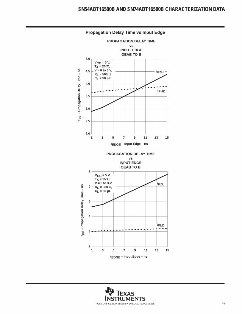
Propagation Delay Time vs Input Edge
2
3
4
5
6
7
1 3 5 7 9 11 13 15
tPZL
tPHZ
2.0
2.5
3.0
3.5
4.0
4.5
5.0
1 3 5 7 9 11 13 15
tEDGE – Input Edge – ns
PROPAGATION DELAY TIMEvs
INPUT EDGEOEAB TO B
PROPAGATION DELAY TIMEvs
INPUT EDGEOEAB TO B
tPZH
tEDGE – Input Edge – ns
tPLZ
t
– P
ropa
gatio
n D
elay
Tim
e –
nspd
t
– P
ropa
gatio
n D
elay
Tim
e –
nspd
VCC = 5 V,TA = 25°C,V = 0 to 3 V,RL = 500 Ω,CL = 50 pF
VCC = 5 V,TA = 25°C,V = 0 to 3 V,RL = 500 Ω,CL = 50 pF
SN54ABT16500B AND SN74ABT16500B CHARACTERIZATION DATA
50 POST OFFICE BOX 655303 • DALLAS, TEXAS 75265
VOHV and VOLP
2
0
–1
–20 10 20 30 40 50
Vol
ts –
V
4
5
17 SWITCHING 1 HIGH LH B → A6
60 70 80
3
1
2
0
–1
–20 10 20 30 40 50
Vol
ts –
V
4
5
17 SWITCHING 1 LOW HL B → A6
60 70 80
3
1
t – Time – ns
t – Time – ns
VCC = 5 V,TA = 25°C
VCC = 5 V,TA = 25°C
VOHV = Minimum (valley) voltage induced on a quiescent high-level output during switching of other outputs.VOLP = Maximum (peak) voltage induced on a quiescent low-level output during switching of other outputs.
SN54ABT16500B AND SN74ABT16500B CHARACTERIZATION DATA
51POST OFFICE BOX 655303 • DALLAS, TEXAS 75265
Typical Characteristics
0
0.5
1.0
1.5
2.0
2.5
3.0
3.5
4.0
–100 –80 –60 –40 –20 0
IOH – High-Level Output Current – mA
HIGH-LEVEL OUTPUT VOLTAGEvs
HIGH-LEVEL OUTPUT CURRENT
0
0.2
0.4
0.6
0.8
1.0
0 10 20 30 40 50 60 70 80 90 100
LOW-LEVEL OUTPUT VOLTAGEvs
LOW-LEVEL OUTPUT CURRENT
–
Hifh
-Lev
el O
utpu
t Vol
tage
– V
V OH
– L
ow-L
evel
Out
put V
olta
ge –
VV
OL
IOH – High-Level Output Current – mA
VCC = 5 V,TA = 25°C
VCC = 5 V,TA = 25°C
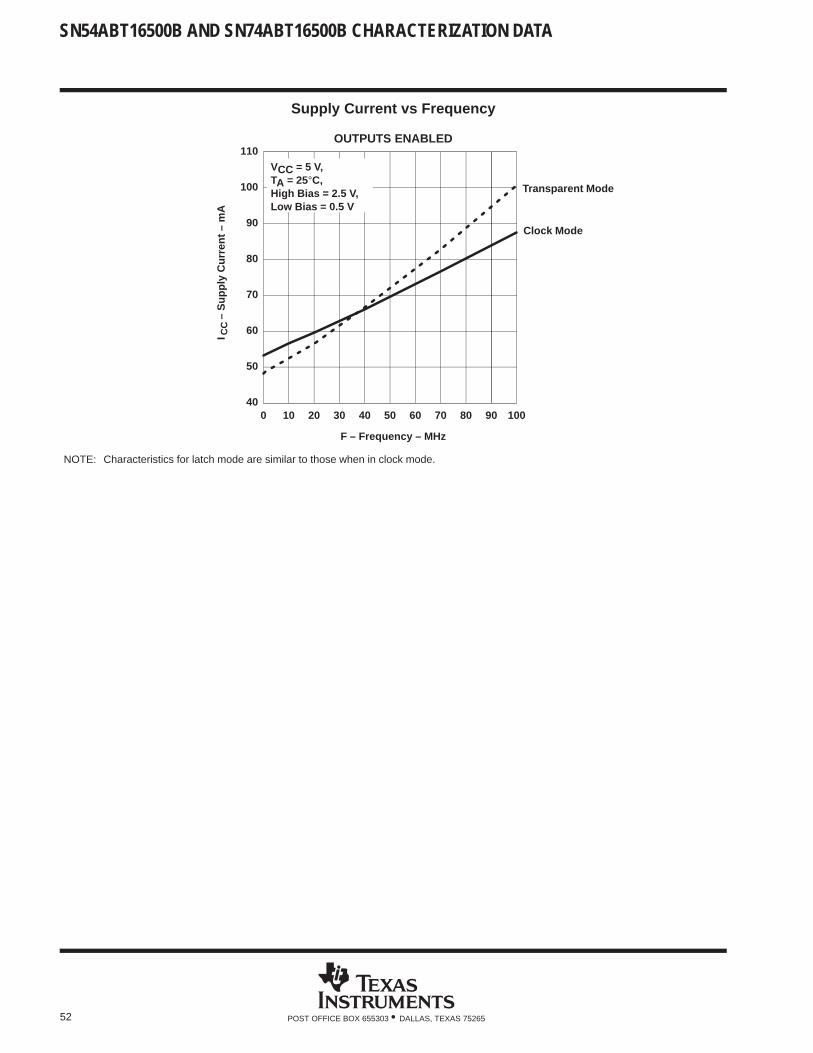
SN54ABT16500B AND SN74ABT16500B CHARACTERIZATION DATA
52 POST OFFICE BOX 655303 • DALLAS, TEXAS 75265
Supply Current vs Frequency
40
50
60
70
80
90
100
110
0 10 20 30 40 50 60 70 80 90 100
F – Frequency – MHz
OUTPUTS ENABLED
– S
uppl
y C
urre
nt –
mA
CC
I
Transparent Mode
Clock Mode
VCC = 5 V,TA = 25°C,High Bias = 2.5 V,Low Bias = 0.5 V
NOTE: Characteristics for latch mode are similar to those when in clock mode.
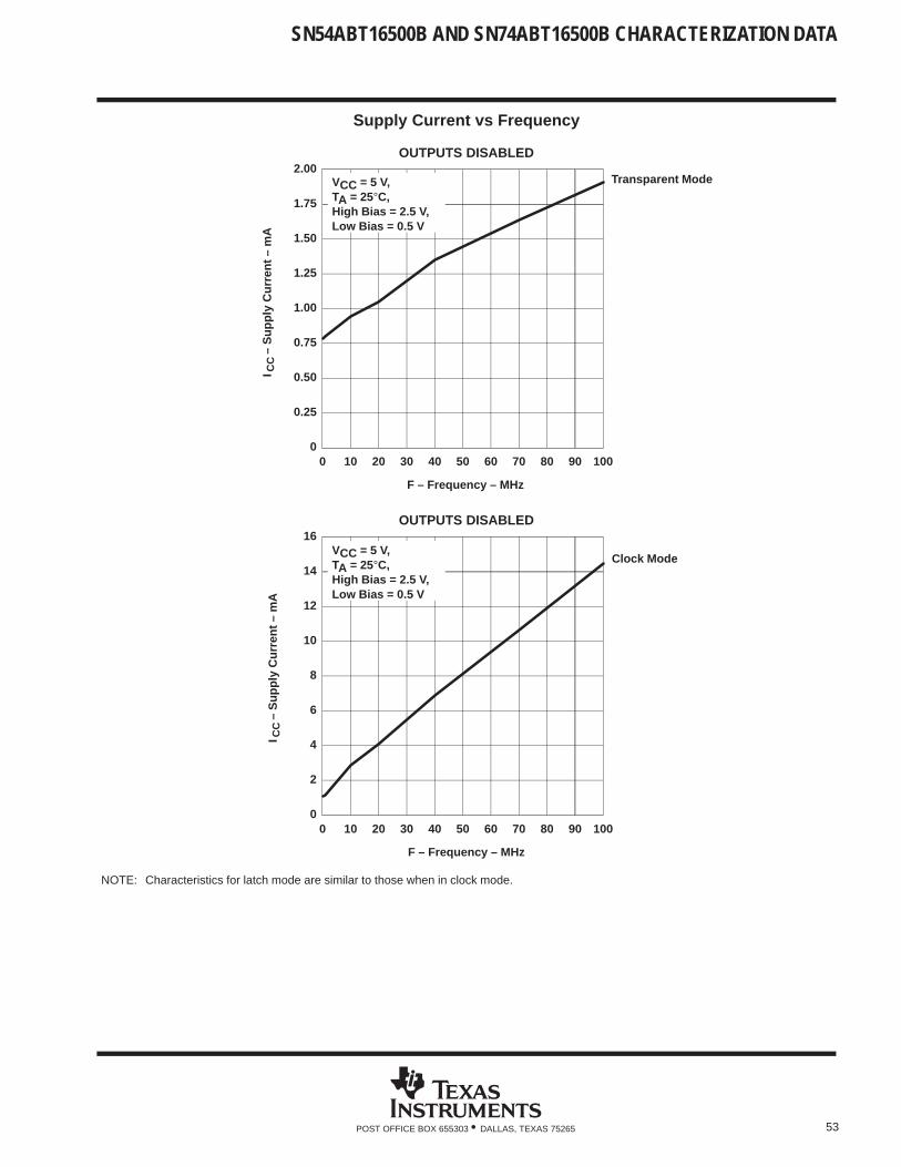
SN54ABT16500B AND SN74ABT16500B CHARACTERIZATION DATA
53POST OFFICE BOX 655303 • DALLAS, TEXAS 75265
Supply Current vs Frequency
0
0.25
0.50
0.75
1.00
1.25
1.50
1.75
2.00
0 10 20 30 40 50 60 70 80 90 100
F – Frequency – MHz
OUTPUTS DISABLED
0
2
4
6
8
10
12
14
16
0 10 20 30 40 50 60 70 80 90 100
F – Frequency – MHz
OUTPUTS DISABLED
Transparent Mode
Clock Mode
– S
uppl
y C
urre
nt –
mA
CC
I
–
Sup
ply
Cur
rent
– m
AC
CI
VCC = 5 V,TA = 25°C,High Bias = 2.5 V,Low Bias = 0.5 V
VCC = 5 V,TA = 25°C,High Bias = 2.5 V,Low Bias = 0.5 V
NOTE: Characteristics for latch mode are similar to those when in clock mode.

SN54ABT16500B AND SN74ABT16500B CHARACTERIZATION DATA
54 POST OFFICE BOX 655303 • DALLAS, TEXAS 75265