Embed Size (px)
Citation preview
Acoustical Analysis Unit
By
Kristine Cabrera
Kevin Chen
Joseph Shim
Design Review Ver. 3 for ECE 445, Senior Design, Spring 2013
TA: Ryan Corey
March 11, 2013
Project No. 14
Contents
1 Introduction . . . . . . . . . . . . . . . . . . . . . . . . . . . . . . . . . . . . . . . . . . . . . . . . . . . . . . . . . . . . . . . 1
1.1 Statement of Purpose . . . . . . . . . . . . . . . . . . . . . . . . . . . . . . . . . . . . . . . . . . . . . . . . . . . . . . 1
1.2 Objectives . . . . . . . . . . . . . . . . . . . . . . . . . . . . . . . . . . . . . . . . . . . . . . . . . . . . . . . . . . . . . . 1
1.2.1 Goals . . . . . . . . . . . . . . . . . . . . . . . . . . . . . . . . . . . . . . . . . . . . . . . . . . . . . . . . . . . . . . 1
1.2.2 Functions . . . . . . . . . . . . . . . . . . . . . . . . . . . . . . . . . . . . . . . . . . . . . . . . . . . . . . . . . . . 1
1.2.3 Benefits & Features . . . . . . . . . . . . . . . . . . . . . . . . . . . . . . . . . . . . . . . . . . . . . . . . . . . . 1
2 Design. . . . . . . . . . . . . . . . . . . . . . . . . . . . . . . . . . . . . . . . . . . . . . . . . . . . . . . . . . . . . . . . . . . . 3
2.1 Block Diagrams . . . . . . . . . . . . . . . . . . . . . . . . . . . . . . . . . . . . . . . . . . . . . . . . . . . . . . . . . . 3
2.2 Block Diagram Details . . . . . . . . . . . . . . . . . . . . . . . . . . . . . . . . . . . . . . . . . . . . . . . . . . . . . 6
2.2.1 Module Descriptions. . . . . . . . . . . . . . . . . . . . . . . . . . . . . . . . . . . . . . . . . . . . . . . . . . . . 6
2.2.2 Power . . . . . . . . . . . . . . . . . . . . . . . . . . . . . . . . . . . . . . . . . . . . . . . . . . . . . . . . . . . . . . 8
2.2.3 Analog . . . . . . . . . . . . . . . . . . . . . . . . . . . . . . . . . . . . . . . . . . . . . . . . . . . . . . . . . . . . . 12
2.2.4 ADC . . . . . . . . . . . . . . . . . . . . . . . . . . . . . . . . . . . . . . . . . . . . . . . . . . . . . . . . . . . . . . . 15
2.2.5 Microcontroller . . . . . . . . . . . . . . . . . . . . . . . . . . . . . . . . . . . . . . . . . . . . . . . . . . . . . . . 17
2.2.6 LCD . . . . . . . . . . . . . . . . . . . . . . . . . . . . . . . . . . . . . . . . . . . . . . . . . . . . . . . . . . . . . . . 20
2.3 Additional Schematics and Pin Assignments . . . . . . . . . . . . . . . . . . . . . . . . . . . . . . . . . . . . . . 21
2.4 Performance Requirements . . . . . . . . . . . . . . . . . . . . . . . . . . . . . . . . . . . . . . . . . . . . . . . . . . 26
2.5 Testing Procedures . . . . . . . . . . . . . . . . . . . . . . . . . . . . . . . . . . . . . . . . . . . . . . . . . . . . . . . . 27
2.6 Tolerance Analysis . . . . . . . . . . . . . . . . . . . . . . . . . . . . . . . . . . . . . . . . . . . . . . . . . . . . . . . . 34
2.7 Ethical Issues . . . . . . . . . . . . . . . . . . . . . . . . . . . . . . . . . . . . . . . . . . . . . . . . . . . . . . . . . . . . 34
2.8 Safety Issues . . . . . . . . . . . . . . . . . . . . . . . . . . . . . . . . . . . . . . . . . . . . . . . . . . . . . . . . . . . . . 35
3 Cost and Schedule . . . . . . . . . . . . . . . . . . . . . . . . . . . . . . . . . . . . . . . . . . . . . . . . . . . . . . . . . . . 36
3.1 Cost Analysis . . . . . . . . . . . . . . . . . . . . . . . . . . . . . . . . . . . . . . . . . . . . . . . . . . . . . . . . . . . . 36
3.2 Timeline. . . . . . . . . . . . . . . . . . . . . . . . . . . . . . . . . . . . . . . . . . . . . . . . . . . . . . . . . . . . . . . . 37
4 Contingency Plan. . . . . . . . . . . . . . . . . . . . . . . . . . . . . . . . . . . . . . . . . . . . . . . . . . . . . . . . . . . . 38
5 References . . . . . . . . . . . . . . . . . . . . . . . . . . . . . . . . . . . . . . . . . . . . . . . . . . . . . . . . . . . . . . . . . 39
2
1 Introduction
1.1 Statement of Purpose
The goal of this project is to design an acoustical analysis unit that will be used for research. Professor
Swenson and Dr. White presented this project idea to the senior design class. The final product should be
able to do real time analysis of acoustical waves between 20Hz to around 10kHz and show the data in a
simple and clean manner. Our device should be able to take input from a microphone probe, such as the
Brel & Kjr microphones that the army acoustics research lab possesses. The resulting waveforms will be
display or analyzed by the device, as the user commands. The user will be able to treat this like any other
lab equipment, as it will have several menus and user inputs for navigation. All hardware and software will
be properly documented so that the research team will be able to add on new functions as needed, making
it far better than any consumer off the shelf equipment.
1.2 Objectives
1.2.1 Goals
• Create a device capable of being more portable to be used outdoors and that can be used with different
types of microphones
• Use audio inputs from microphones to graph and collect acoustic intensity
• Have modularity in programming to allow additional data collection, functionality, calculations, etc.
for end customer
1.2.2 Functions
• Inputs audio from microphones
• Distinguishes what noise/audio coming from each microphone
• Outputs acoustic intensity in the form of moving graphical bars
• Has various physical buttons for menus
1.2.3 Benefits & Features
The current device used for acoustical analysis with microphone probes is quite cumbersome and heavy to
carry around in the field. This is not very suitable for the reason that the microphones and device need to
be portable in order to be brought around outdoors. As for the user interface, it is quite difficult and not
intuitive since there are too many buttons and options. Dr. Swenson and Dr. White would like the device
to be more user-friendly and more efficient when trying to take in audio data from the microphone probes.
Also, they would like the software to be modular such that it can be easier to add different functions.
So, our device will solve these by being able to:
• Be smaller and lighter for ease of use outdoors
1
• Have an intuitive program that is capable to be easily modified to increase the amount of functions
• Be compatible with the existing 2-probe microphone (BNC connections)
As of right now, the screen on the original device is quite dark. We chose to implement a large 3.5 inch LCD
with a backlight. This would give the device a cleaner look without sacrificing any of the data/menus that
need to be shown.
Our device will have an intuitive program and interface so that Dr. Swenson, Dr. White, or other individuals
would like to refine the functions already implemented or input additional functions. The user interface
should be spread out nicely and not have too many menus. There should be a clear and understandable way
of getting the desired function.
2
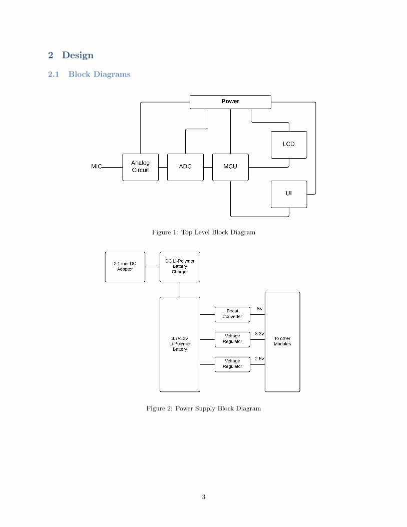
2 Design
2.1 Block Diagrams
Figure 1: Top Level Block Diagram
Figure 2: Power Supply Block Diagram
3
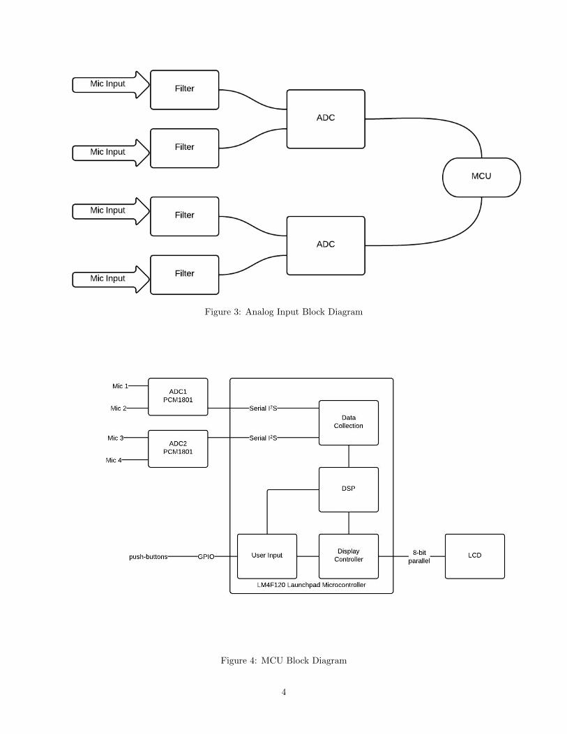
Figure 3: Analog Input Block Diagram
Figure 4: MCU Block Diagram
4
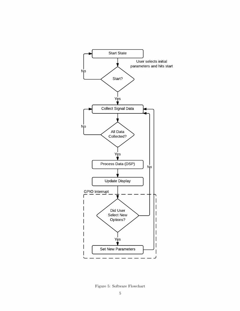
Figure 5: Software Flowchart
5
2.2 Block Diagram Details
2.2.1 Module Descriptions
Summary
The acoustic analyzer unit will consist of 3 main parts: power, MCU, and display. The overall system will
take the audio from the microphones, process it, and show it to the user through the display. The user
can make the system display the specific data that he/she wants and in the form he/she wants through
manipulation of the user interface. If there are extra functions that the user needs that are not already
preprogrammed, he/she can add them through the programmer.
Microcontroller
This module controls all the digital components of the system. It receives signal data from the ADC and
inputs from the user via pushbuttons, processes the data, and then outputs it to the LCD. This module
handles all the digital signal processing of the incoming audio signal data. It is also responsible for the GUI
for the user and the users inputs. The sub-modules of this module are all parts of the software code.
1. Data Collection: The data collection sub-module handles acquiring the audio data from the two
external ADC units. Once the sub-module has acquired all 4 sets of audio data (one from each
microphone, two from each ADC), it passes the data to the DSP sub-module for processing.
2. Digital Signal Processing (DSP): The DSP sub-module handles all the processing of the audio
data. The sub-module will initially only include the FFT of the audio data as part of the functionality.
There will be functionality included to let the user add their own DSP functions to process the data.
Once the data is processed, it will be passed to the display controller sub-module.
3. Display Controller This sub-module will update the LCD with the data obtained from the DSP sub-
module. This module is also responsible for the GUI and manipulation of the GUI based on incoming
inputs from the user input sub-module.
Power Module
This provides different voltages and power to the other modules: Analog circuit, ADC, Microcontroller, and
LCD screen.
Analog-to-Digital Converter (ADC) Module
The Analog-to-Digital converter units are part of the input system. The ADCs convert the analog voltage
signals received into a digital form for use by the microcontroller.
Analog
The audio block consists of the analog circuitry that will take the audio signal from the microphones to the
MCU. The input will have to be able to take in a frequency range between 20Hz to around 10kHz. In order
to do this a chunk of the circuit will be the anti-aliasing filter that will have an upper 3dB rolloff around
11kHz.
6
The audio block consists of the analog circuitry that will take the audio signal from the microphones to the
MCU. The circuitry will include any preamplification, filtering, and buffering that’s needed and will provide
a usable signal for the MCU’s ADC as well as protecting the Microphone from any electrical damage and
vice versa.
User Interface
The user input sub-module takes the input signals from the external push-buttons and manipulates the DSP
settings and GUI settings accordingly
Display
This module displays the processed audio data on a LCD screen for the user.
7
2.2.2 Power
Inputs: The input is the battery source, which can be recharged via wall outlet.
Outputs: The 3.7/4.2V battery voltage will be boosted to 5V (for part of the analog circuitry, the ADC,
and the LCD). It will be stepped down to 3.3V for the Microcontroller and to 2.5V for part of the analog
circuitry.
Description: The main source of power is from a 3.7/4.2V Li-polymer battery. This battery can be
recharged via wall outlet. We need both lower and higher voltages that the battery provides. Below is a
table explaining the voltages needed:
Table 1: Voltage Requirements
Module Required Voltage
Analog Circuitry 2.5V & 5V
ADC 5V
Clock Chip 3.3V
Microcontroller 3.3V
LCD Screen 5V
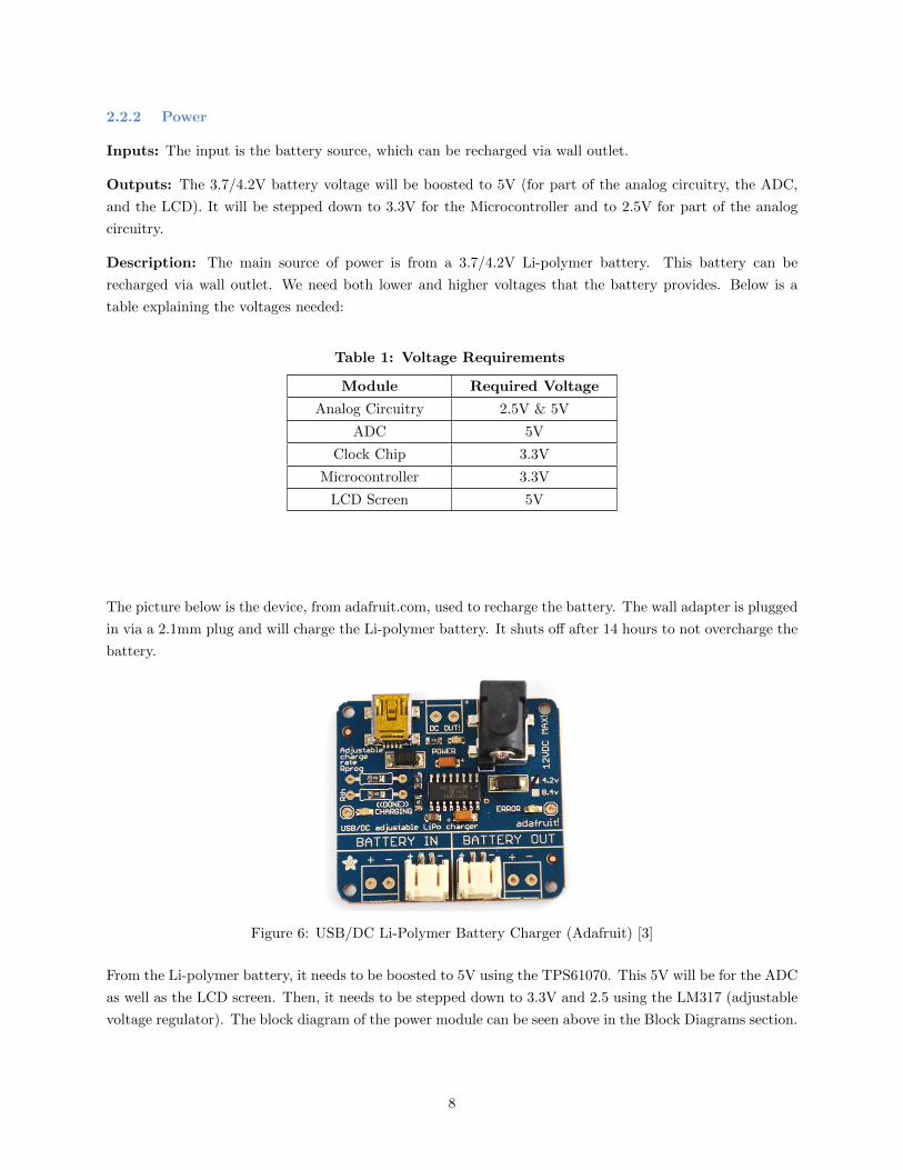
The picture below is the device, from adafruit.com, used to recharge the battery. The wall adapter is plugged
in via a 2.1mm plug and will charge the Li-polymer battery. It shuts off after 14 hours to not overcharge the
battery.
Figure 6: USB/DC Li-Polymer Battery Charger (Adafruit) [3]
From the Li-polymer battery, it needs to be boosted to 5V using the TPS61070. This 5V will be for the ADC
as well as the LCD screen. Then, it needs to be stepped down to 3.3V and 2.5 using the LM317 (adjustable
voltage regulator). The block diagram of the power module can be seen above in the Block Diagrams section.
8
Simulations and Calculations
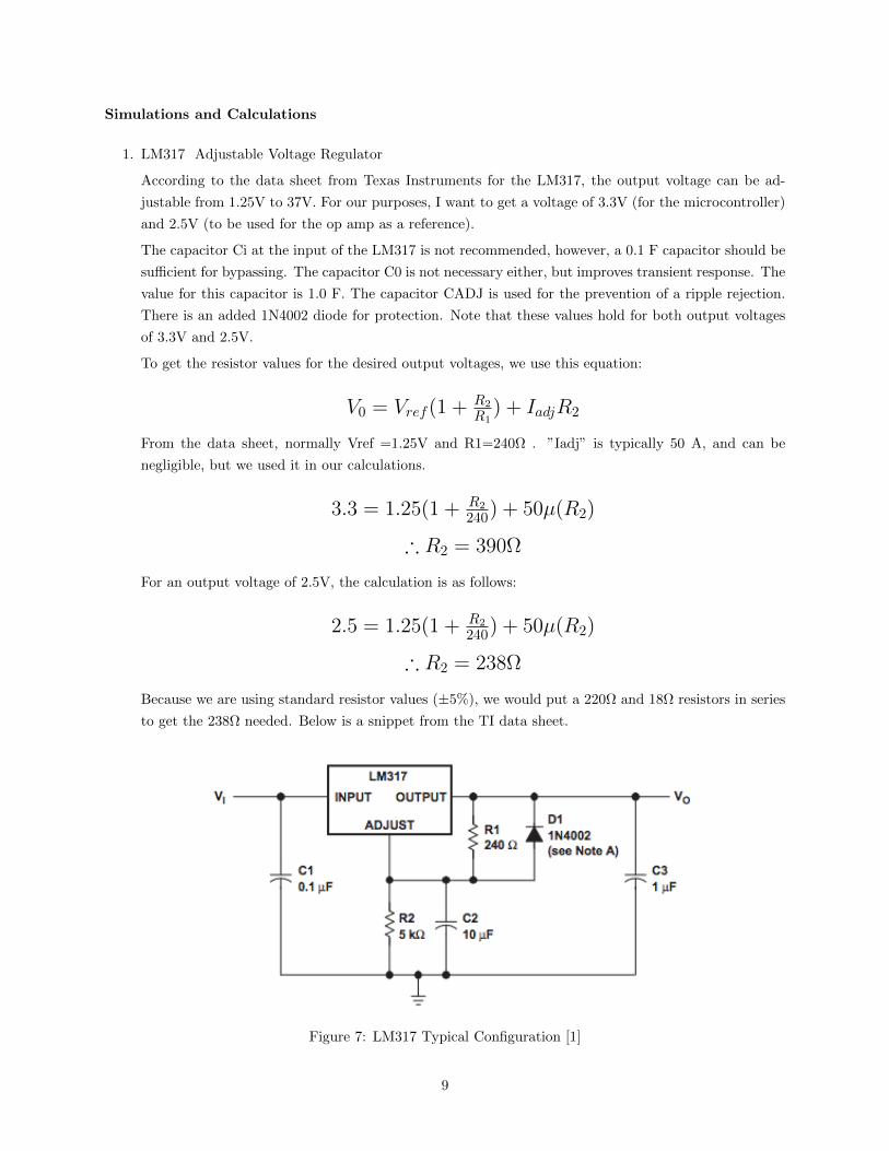
1. LM317 Adjustable Voltage Regulator
According to the data sheet from Texas Instruments for the LM317, the output voltage can be ad-
justable from 1.25V to 37V. For our purposes, I want to get a voltage of 3.3V (for the microcontroller)
and 2.5V (to be used for the op amp as a reference).
The capacitor Ci at the input of the LM317 is not recommended, however, a 0.1 F capacitor should be
sufficient for bypassing. The capacitor C0 is not necessary either, but improves transient response. The
value for this capacitor is 1.0 F. The capacitor CADJ is used for the prevention of a ripple rejection.
There is an added 1N4002 diode for protection. Note that these values hold for both output voltages
of 3.3V and 2.5V.
To get the resistor values for the desired output voltages, we use this equation:
V0 = Vref(1 + R2
R1) + IadjR2
From the data sheet, normally Vref =1.25V and R1=240Ω . ”Iadj” is typically 50 A, and can be
negligible, but we used it in our calculations.
3.3 = 1.25(1 + R2
240) + 50µ(R2)
∴ R2 = 390Ω
For an output voltage of 2.5V, the calculation is as follows:
2.5 = 1.25(1 + R2
240) + 50µ(R2)
∴ R2 = 238Ω
Because we are using standard resistor values (±5%), we would put a 220Ω and 18Ω resistors in series
to get the 238Ω needed. Below is a snippet from the TI data sheet.
Figure 7: LM317 Typical Configuration [1]
9
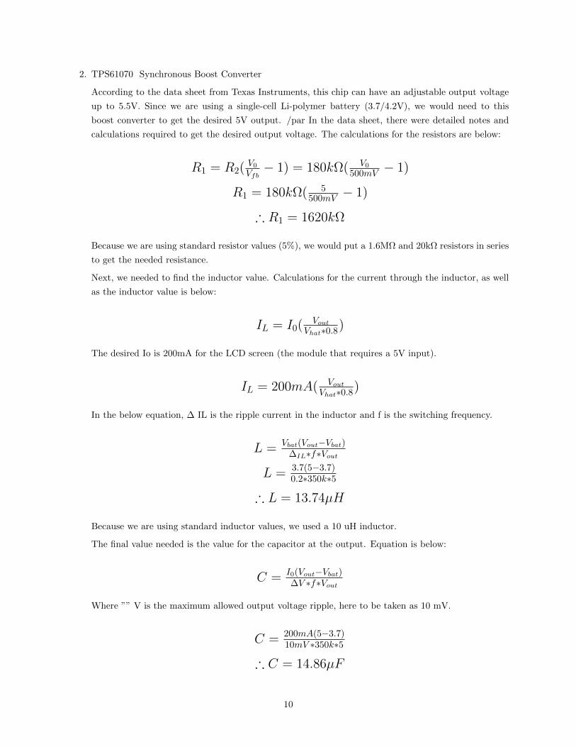
2. TPS61070 Synchronous Boost Converter
According to the data sheet from Texas Instruments, this chip can have an adjustable output voltage
up to 5.5V. Since we are using a single-cell Li-polymer battery (3.7/4.2V), we would need to this
boost converter to get the desired 5V output. /par In the data sheet, there were detailed notes and
calculations required to get the desired output voltage. The calculations for the resistors are below:
R1 = R2(V0
Vfb− 1) = 180kΩ( V0
500mV − 1)
R1 = 180kΩ( 5500mV − 1)
∴ R1 = 1620kΩ
Because we are using standard resistor values (5%), we would put a 1.6MΩ and 20kΩ resistors in series
to get the needed resistance.
Next, we needed to find the inductor value. Calculations for the current through the inductor, as well
as the inductor value is below:
IL = I0(Vout
Vhat∗0.8)
The desired Io is 200mA for the LCD screen (the module that requires a 5V input).
IL = 200mA( Vout
Vhat∗0.8)
In the below equation, ∆ IL is the ripple current in the inductor and f is the switching frequency.
L = Vbat(Vout−Vbat)∆IL∗f∗Vout
L = 3.7(5−3.7)0.2∗350k∗5
∴ L = 13.74µH
Because we are using standard inductor values, we used a 10 uH inductor.
The final value needed is the value for the capacitor at the output. Equation is below:
C = I0(Vout−Vbat)∆V ∗f∗Vout
Where ”” V is the maximum allowed output voltage ripple, here to be taken as 10 mV.
C = 200mA(5−3.7)10mV ∗350k∗5
∴ C = 14.86µF
10
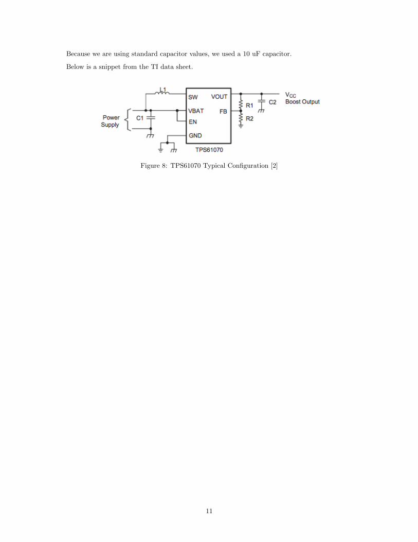
Because we are using standard capacitor values, we used a 10 uF capacitor.
Below is a snippet from the TI data sheet.
Figure 8: TPS61070 Typical Configuration [2]
11
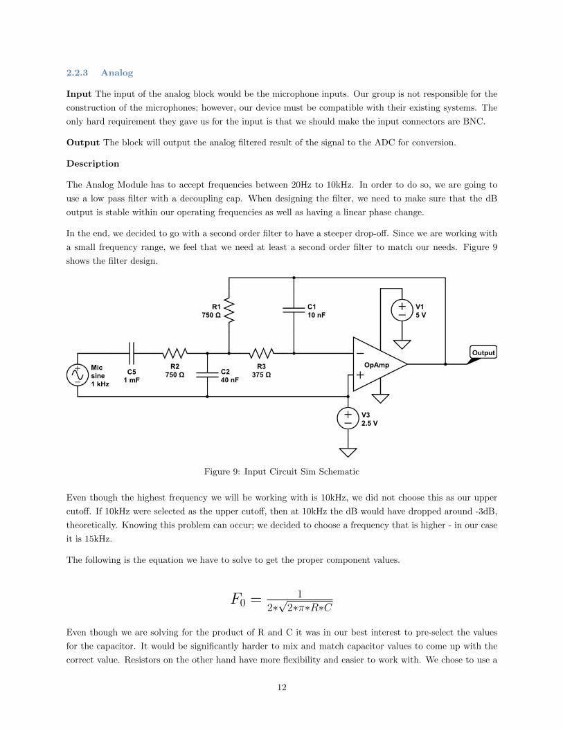
2.2.3 Analog
Input The input of the analog block would be the microphone inputs. Our group is not responsible for the
construction of the microphones; however, our device must be compatible with their existing systems. The
only hard requirement they gave us for the input is that we should make the input connectors are BNC.
Output The block will output the analog filtered result of the signal to the ADC for conversion.
Description
The Analog Module has to accept frequencies between 20Hz to 10kHz. In order to do so, we are going to
use a low pass filter with a decoupling cap. When designing the filter, we need to make sure that the dB
output is stable within our operating frequencies as well as having a linear phase change.
In the end, we decided to go with a second order filter to have a steeper drop-off. Since we are working with
a small frequency range, we feel that we need at least a second order filter to match our needs. Figure 9
shows the filter design.
Figure 9: Input Circuit Sim Schematic
Even though the highest frequency we will be working with is 10kHz, we did not choose this as our upper
cutoff. If 10kHz were selected as the upper cutoff, then at 10kHz the dB would have dropped around -3dB,
theoretically. Knowing this problem can occur; we decided to choose a frequency that is higher - in our case
it is 15kHz.
The following is the equation we have to solve to get the proper component values.
F0 =1
2∗√
2∗π∗R∗C
Even though we are solving for the product of R and C it was in our best interest to pre-select the values
for the capacitor. It would be significantly harder to mix and match capacitor values to come up with the
correct value. Resistors on the other hand have more flexibility and easier to work with. We chose to use a
12
.01uF capacitor which is a standard and abundant value.
15kHz = 12∗√
2∗π∗R∗.01µF
The selection of our OpAmp was determined by several factors such as the amount of noise, bandwidth,
supply voltages, settling time, and also based on the applications notes of the datasheets. The OpAmp that
was chosen is the OPA227PA that has the following specifications
• low noise @ 3nV/Hz
• wide bandwidth @ 8MHz
• settling time @ 5us
• open loop gain @ 160dB
• input bias current @ 10nA
• offset voltage max @ 75uV
• supply voltage @ ±2.5V to ±18V
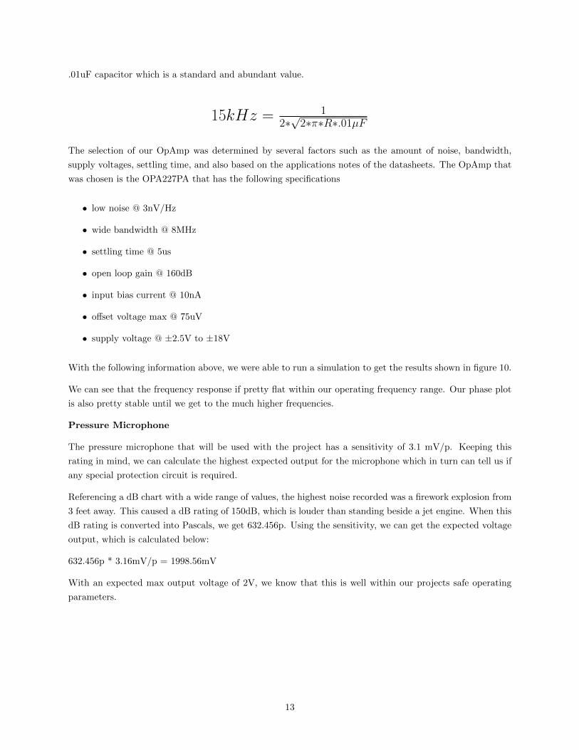
With the following information above, we were able to run a simulation to get the results shown in figure 10.
We can see that the frequency response if pretty flat within our operating frequency range. Our phase plot
is also pretty stable until we get to the much higher frequencies.
Pressure Microphone
The pressure microphone that will be used with the project has a sensitivity of 3.1 mV/p. Keeping this
rating in mind, we can calculate the highest expected output for the microphone which in turn can tell us if
any special protection circuit is required.
Referencing a dB chart with a wide range of values, the highest noise recorded was a firework explosion from
3 feet away. This caused a dB rating of 150dB, which is louder than standing beside a jet engine. When this
dB rating is converted into Pascals, we get 632.456p. Using the sensitivity, we can get the expected voltage
output, which is calculated below:
632.456p * 3.16mV/p = 1998.56mV
With an expected max output voltage of 2V, we know that this is well within our projects safe operating
parameters.
13
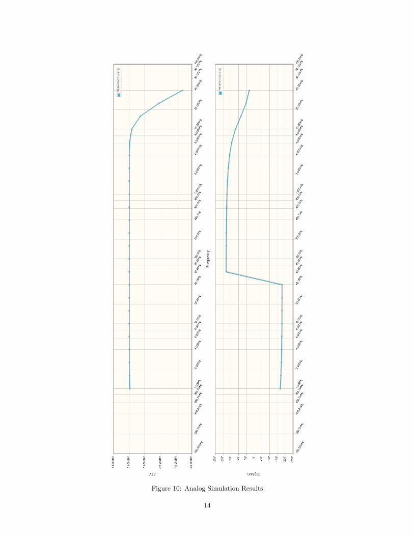
Figure 10: Analog Simulation Results
14
2.2.4 ADC
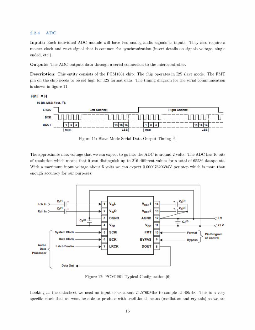
Inputs: Each individual ADC module will have two analog audio signals as inputs. They also require a
master clock and reset signal that is common for synchronization.(insert details on signals voltage, single
ended, etc.)
Outputs: The ADC outputs data through a serial connection to the microcontroller.
Description: This entity consists of the PCM1801 chip. The chip operates in I2S slave mode. The FMT
pin on the chip needs to be set high for I2S format data. The timing diagram for the serial communication
is shown in figure 11.
Figure 11: Slave Mode Serial Data Output Timing [6]
The approximite max voltage that we can expect to go into the ADC is around 2 volts. The ADC has 16 bits
of resolution which means that it can distinguish up to 216 different values for a total of 65536 datapoints.
With a maximum input voltage about 5 volts we can expect 0.00007629394V per step which is more than
enough accuracy for our purposes.
Figure 12: PCM1801 Typical Configuration [6]
Looking at the datasheet we need an input clock about 24.5760Mhz to sample at 48kHz. This is a very
specific clock that we wont be able to produce with traditional means (oscillators and crystals) so we are
15
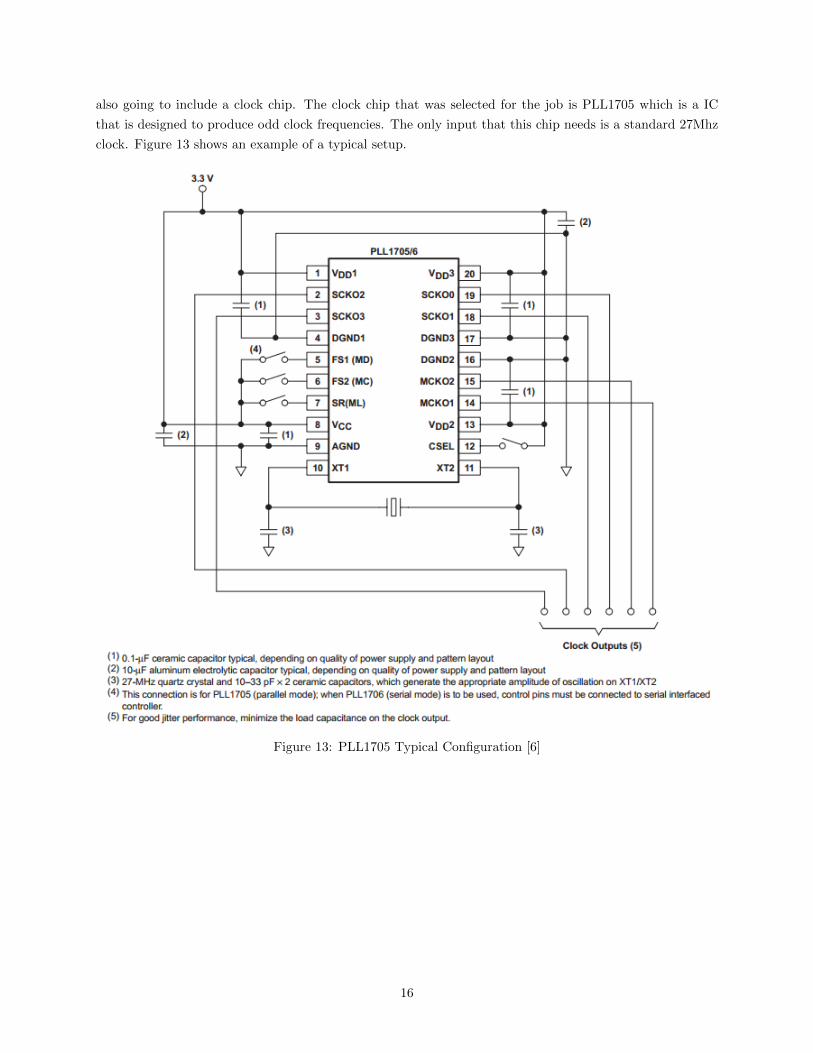
also going to include a clock chip. The clock chip that was selected for the job is PLL1705 which is a IC
that is designed to produce odd clock frequencies. The only input that this chip needs is a standard 27Mhz
clock. Figure 13 shows an example of a typical setup.
Figure 13: PLL1705 Typical Configuration [6]
16
2.2.5 Microcontroller
1. Data Collection
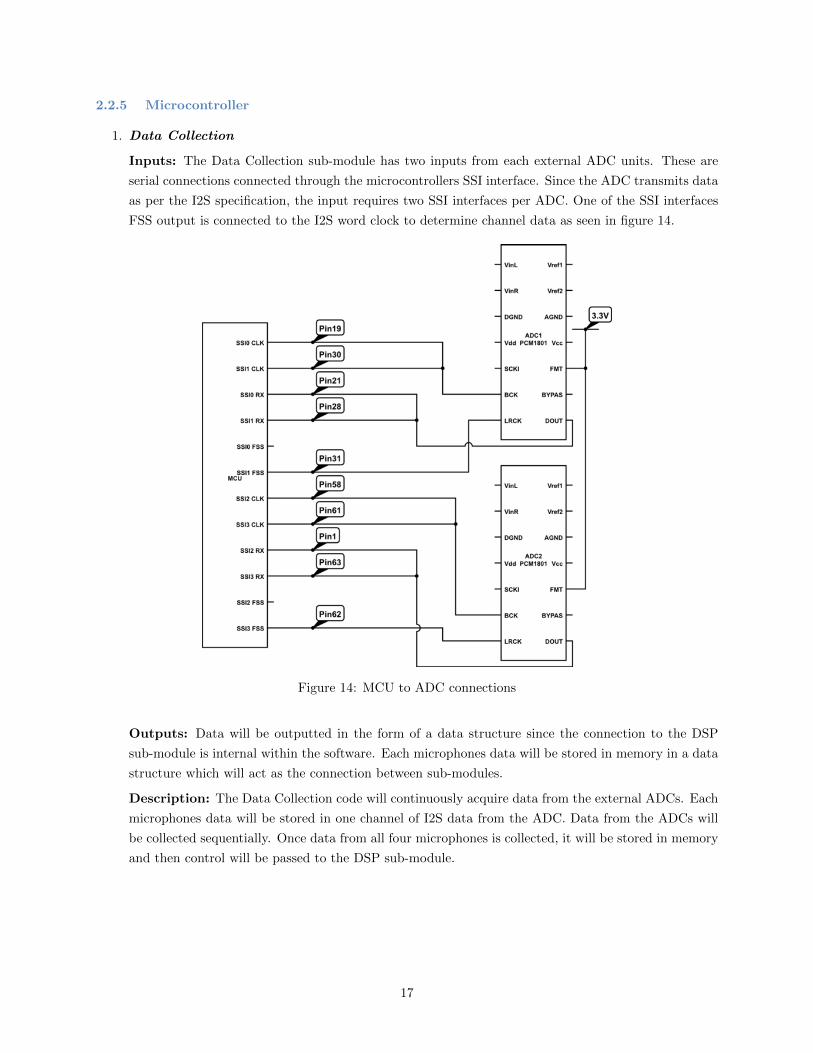
Inputs: The Data Collection sub-module has two inputs from each external ADC units. These are
serial connections connected through the microcontrollers SSI interface. Since the ADC transmits data
as per the I2S specification, the input requires two SSI interfaces per ADC. One of the SSI interfaces
FSS output is connected to the I2S word clock to determine channel data as seen in figure 14.
Figure 14: MCU to ADC connections
Outputs: Data will be outputted in the form of a data structure since the connection to the DSP
sub-module is internal within the software. Each microphones data will be stored in memory in a data
structure which will act as the connection between sub-modules.
Description: The Data Collection code will continuously acquire data from the external ADCs. Each
microphones data will be stored in one channel of I2S data from the ADC. Data from the ADCs will
be collected sequentially. Once data from all four microphones is collected, it will be stored in memory
and then control will be passed to the DSP sub-module.
17
2. Digital Signal Processing
Inputs: Input data comes from the Data Collection sub-module and will be stored in memory where
the DSP sub-module can access it. There will also be input from the user input sub-module in the form
of changes to certain variables in memory that represent the parameters of any DSP functionality.
Outputs: Output data will be stored in memory for the Display Controller sub-module to use. Each
new DSP function implemented by the user will need its own data structure in memory to pass on to
the Display Controller.
Description: When control is passed to the DSP sub-module, the sub-module will extract the data
and process it in each signal processing function set by the user in order. Initially, the DSP sub-
module will only include processing the data via a FFT. After the audio data is processed and saved
in respective data structures in memory, control will be passed to the Display Controller sub-module.
3. User Input
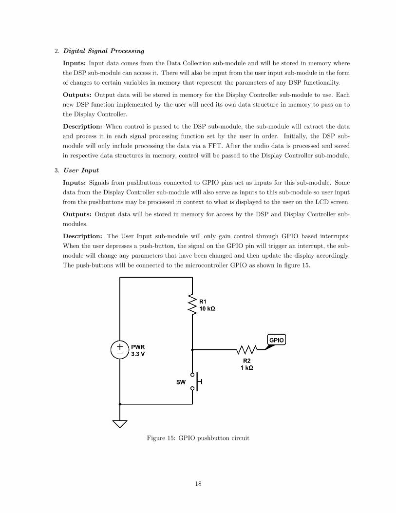
Inputs: Signals from pushbuttons connected to GPIO pins act as inputs for this sub-module. Some
data from the Display Controller sub-module will also serve as inputs to this sub-module so user input
from the pushbuttons may be processed in context to what is displayed to the user on the LCD screen.
Outputs: Output data will be stored in memory for access by the DSP and Display Controller sub-
modules.
Description: The User Input sub-module will only gain control through GPIO based interrupts.
When the user depresses a push-button, the signal on the GPIO pin will trigger an interrupt, the sub-
module will change any parameters that have been changed and then update the display accordingly.
The push-buttons will be connected to the microcontroller GPIO as shown in figure 15.
Figure 15: GPIO pushbutton circuit
18
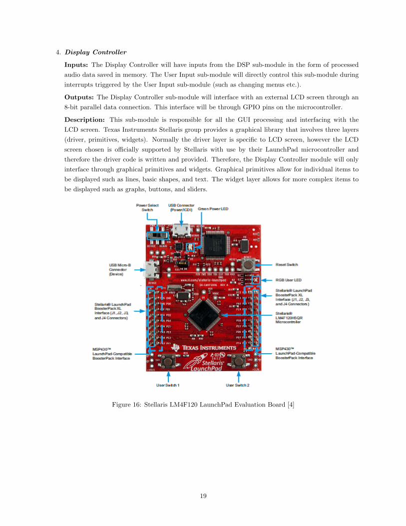
4. Display Controller
Inputs: The Display Controller will have inputs from the DSP sub-module in the form of processed
audio data saved in memory. The User Input sub-module will directly control this sub-module during
interrupts triggered by the User Input sub-module (such as changing menus etc.).
Outputs: The Display Controller sub-module will interface with an external LCD screen through an
8-bit parallel data connection. This interface will be through GPIO pins on the microcontroller.
Description: This sub-module is responsible for all the GUI processing and interfacing with the
LCD screen. Texas Instruments Stellaris group provides a graphical library that involves three layers
(driver, primitives, widgets). Normally the driver layer is specific to LCD screen, however the LCD
screen chosen is officially supported by Stellaris with use by their LaunchPad microcontroller and
therefore the driver code is written and provided. Therefore, the Display Controller module will only
interface through graphical primitives and widgets. Graphical primitives allow for individual items to
be displayed such as lines, basic shapes, and text. The widget layer allows for more complex items to
be displayed such as graphs, buttons, and sliders.
Figure 16: Stellaris LM4F120 LaunchPad Evaluation Board [4]
19
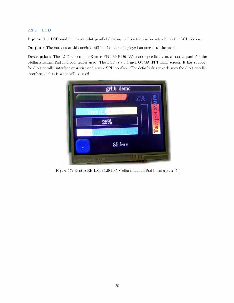
2.2.6 LCD
Inputs: The LCD module has an 8-bit parallel data input from the microcontroller to the LCD screen.
Outputs: The outputs of this module will be the items displayed on screen to the user.
Description: The LCD screen is a Kentec EB-LM4F120-L35 made specifically as a boosterpack for the
Stellaris LaunchPad microcontroller used. The LCD is a 3.5 inch QVGA TFT LCD screen. It has support
for 8-bit parallel interface or 3-wire and 4-wire SPI interface. The default driver code uses the 8-bit parallel
interface so that is what will be used.
Figure 17: Kentec EB-LM4F120-L35 Stellaris LaunchPad boosterpack [5]
20
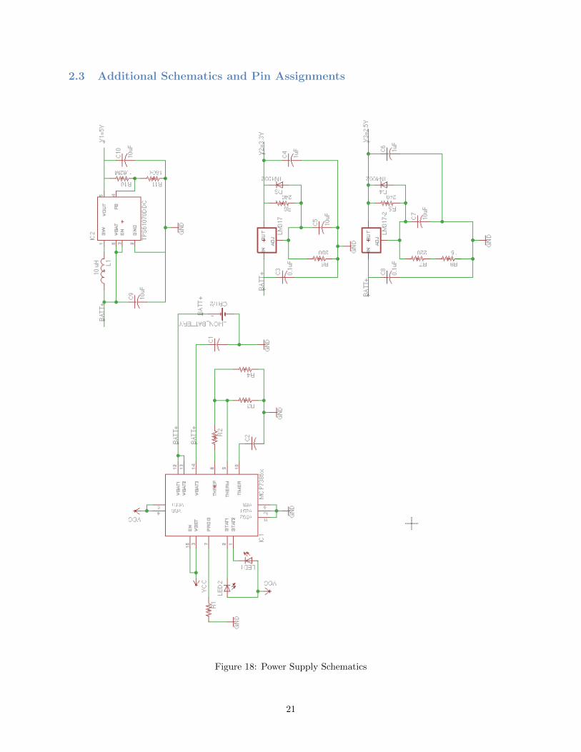
2.3 Additional Schematics and Pin Assignments
Figure 18: Power Supply Schematics
21
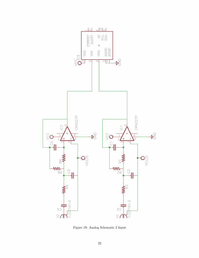
Figure 19: Analog Schematic 2 Input
22
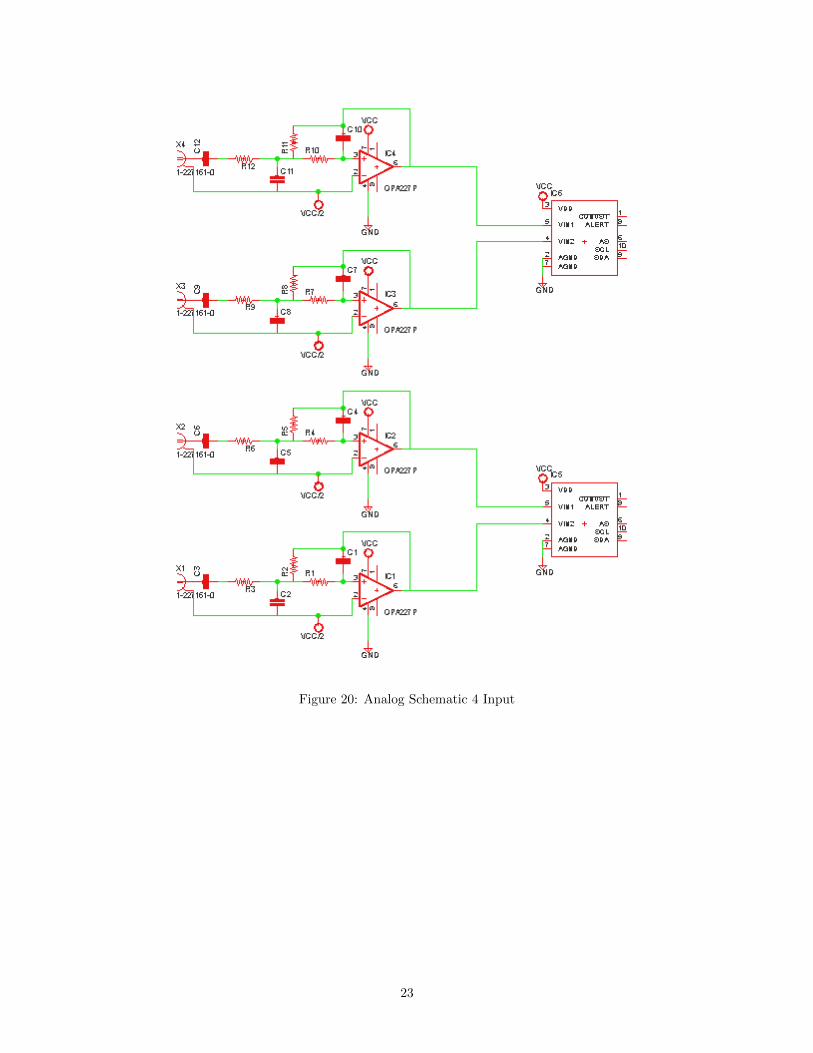
Figure 20: Analog Schematic 4 Input
23
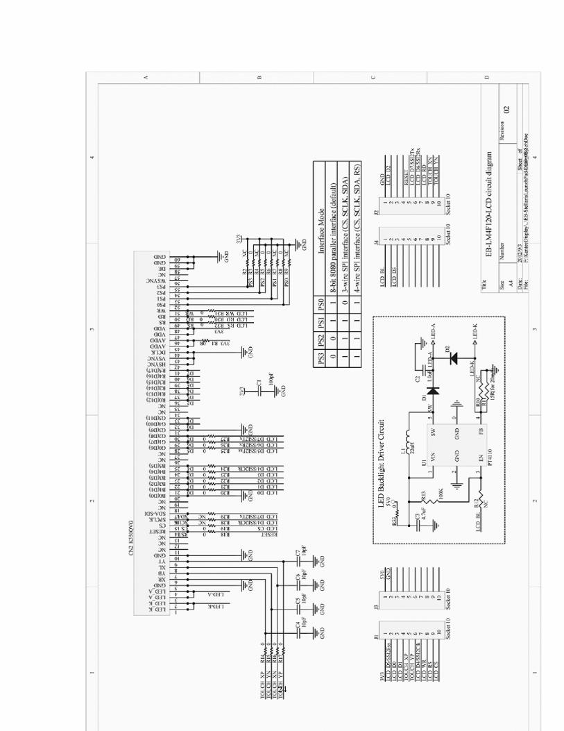
Figure 21: LCD Schematic
24
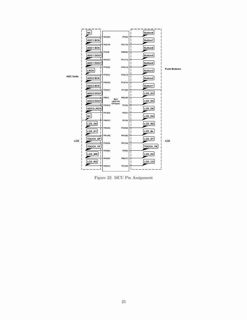
Figure 22: MCU Pin Assignment
25
2.4 Performance Requirements
1. Power
The overall voltage of the power supply ideally should be 2.5, 3.3V, or 5V (but range could be 1V).
The module should be able to provide a stable voltage that the other modules can use. In terms of
efficiency the power supply should have an efficiency rating of over 50.
2. Analog
This module should be able to take input from the microphone and send a usable signal to the MCU.
This should prevent unwanted current/voltages from reaching other modules.
3. ADC
This module needs to successfully digitize the input audio data and send it to the microcontroller
without errors in I2S format.
4. Microcontroller
This module should receive data from the ADCs without error, process the data, and then output it
to the LCD module without error. It also needs to be able to accept user input and act accordingly
depending on what pushbutton is pressed and what is being displayed on the LCD currently.
5. User Interface
There should be ample room for all the buttons to sit on the actual device. The button layout should
be easy to use and prevent multiple buttons from being pressed accidentally.
6. LCD
This module needs to display requested processed audio data correctly and to the users inputted
settings.
26
2.5 Testing Procedures
1. Power
Requirements Summary This should provide enough/stable power and voltages to each of the other
modules that require power.
Verifications Summary Use multimeters to probe the circuit to see if the correct voltage is created
for the different modules. We will also check that voltage/power over time for each module for stability
purposes.
Requirements Verifications
1) Check voltages for 5V, 3.3V, and 2.5V 1) Use a multimeter to check the outputs of the
(Tolerance should be desired voltage ± 0.5V). boost converter (5V) and the two voltage regulators
(3.3V, 2.5V).
2) Supply sufficient voltage each of the modules 2) Use an oscilloscope to see if there is steady
over time. voltage being given to individual module within the
(With a voltage ripple of ± 1.0 V ). voltage ripple.
3) Check individuals modules if 3) Check individual modules
receiving correct voltage. a. Connect all modules to power supply
b. Verify if modules have the correct input voltage
with a multimeter
4) The Charging Circuit 4) Charging Circuit
i. The fully charged battery should be at i. Using a multimeter, check the voltage
maximum 4.2V of battery in initial testing (max 4.2V).
ii. The battery should only at minimum ii. Using a multimeter, check the voltage
3.0V at full discharge. of battery after being connected to various loads
(See Requirement (1)) and must be above 3.0V
iii. With a charge rate of 1000mA, the iii. Connect the battery to the wall outlet and
battery (with rating of 2600mAH) check the amount of time it takes for the battery to
should be fully charged in 2.6 hours be charged to a max 4.2V.
(± 20 min).
27
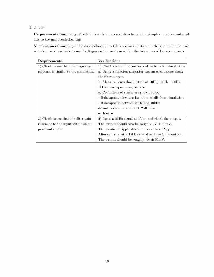
2. Analog
Requirements Summary: Needs to take in the correct data from the microphone probes and send
this to the microcontroller unit.
Verifications Summary: Use an oscilloscope to takes measurements from the audio module. We
will also run stress tests to see if voltages and current are within the tolerances of key components.
Requirements Verifications
1) Check to see that the frequency 1) Check several frequencies and match with simulations
response is similar to the simulation. a. Using a function generator and an oscilloscope check
the filter output.
b. Measurements should start at 20Hz, 100Hz, 500Hz
1kHz then repeat every octave.
c. Conditions of sucess are shown below
- If datapoints deviates less than ±1dB from simulations
- If datapoints between 20Hz and 10kHz
do not deviate more than 0.2 dB from
each other
2) Check to see that the filter gain 2) Input a 5kHz signal at 1Vpp and check the output.
is similar to the input with a small The output should also be roughly 1V ± 50mV.
passband ripple. The passband ripple should be less than .1Vpp
Afterwards input a 15kHz signal and check the output.
The output should be roughly .6v ± 50mV.
28
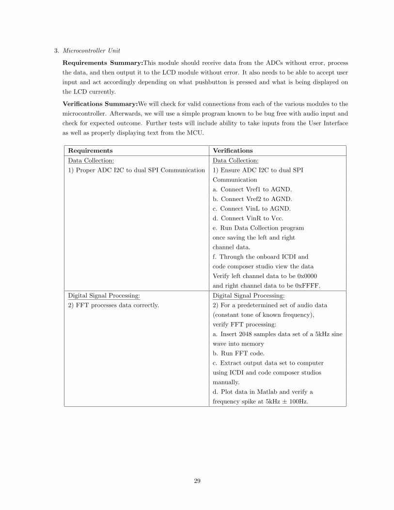
3. Microcontroller Unit
Requirements Summary:This module should receive data from the ADCs without error, process
the data, and then output it to the LCD module without error. It also needs to be able to accept user
input and act accordingly depending on what pushbutton is pressed and what is being displayed on
the LCD currently.
Verifications Summary:We will check for valid connections from each of the various modules to the
microcontroller. Afterwards, we will use a simple program known to be bug free with audio input and
check for expected outcome. Further tests will include ability to take inputs from the User Interface
as well as properly displaying text from the MCU.
Requirements Verifications
Data Collection: Data Collection:
1) Proper ADC I2C to dual SPI Communication 1) Ensure ADC I2C to dual SPI
Communication
a. Connect Vref1 to AGND.
b. Connect Vref2 to AGND.
c. Connect VinL to AGND.
d. Connect VinR to Vcc.
e. Run Data Collection program
once saving the left and right
channel data.
f. Through the onboard ICDI and
code composer studio view the data
Verify left channel data to be 0x0000
and right channel data to be 0xFFFF.
Digital Signal Processing: Digital Signal Processing:
2) FFT processes data correctly. 2) For a predetermined set of audio data
(constant tone of known frequency),
verify FFT processing:
a. Insert 2048 samples data set of a 5kHz sine
wave into memory
b. Run FFT code.
c. Extract output data set to computer
using ICDI and code composer studios
manually.
d. Plot data in Matlab and verify a
frequency spike at 5kHz ± 100Hz.
29
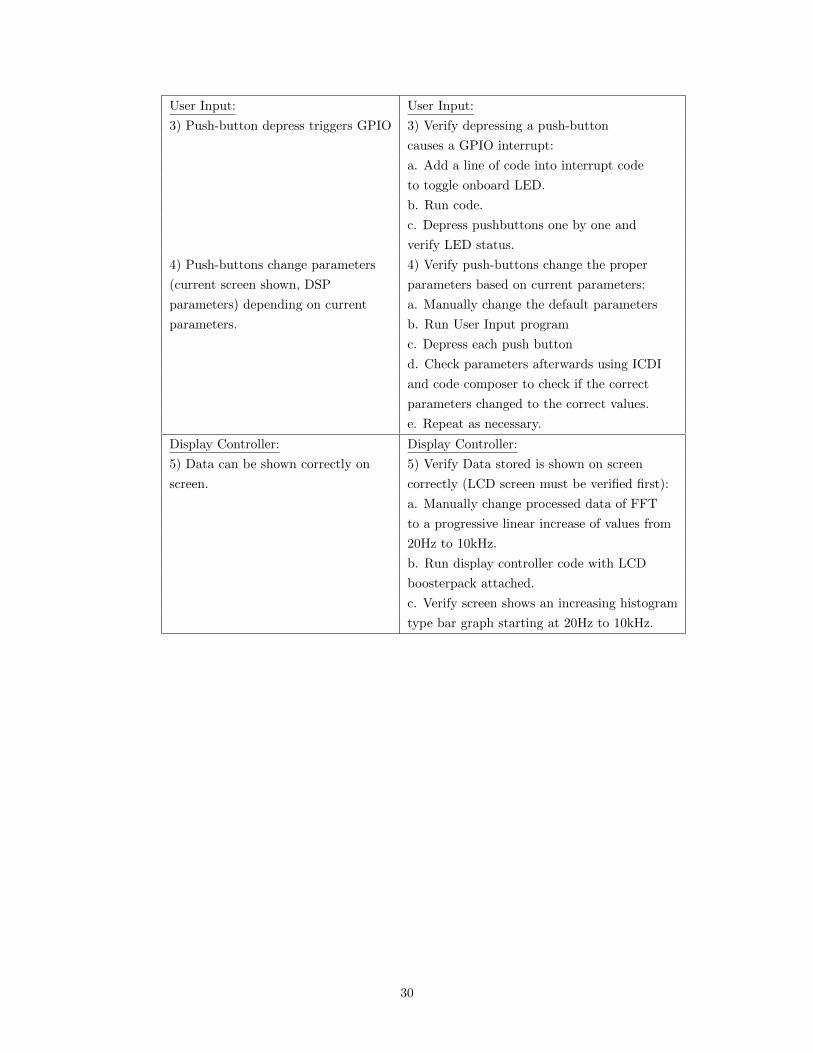
User Input: User Input:
3) Push-button depress triggers GPIO 3) Verify depressing a push-button
causes a GPIO interrupt:
a. Add a line of code into interrupt code
to toggle onboard LED.
b. Run code.
c. Depress pushbuttons one by one and
verify LED status.
4) Push-buttons change parameters 4) Verify push-buttons change the proper
(current screen shown, DSP parameters based on current parameters:
parameters) depending on current a. Manually change the default parameters
parameters. b. Run User Input program
c. Depress each push button
d. Check parameters afterwards using ICDI
and code composer to check if the correct
parameters changed to the correct values.
e. Repeat as necessary.
Display Controller: Display Controller:
5) Data can be shown correctly on 5) Verify Data stored is shown on screen
screen. correctly (LCD screen must be verified first):
a. Manually change processed data of FFT
to a progressive linear increase of values from
20Hz to 10kHz.
b. Run display controller code with LCD
boosterpack attached.
c. Verify screen shows an increasing histogram
type bar graph starting at 20Hz to 10kHz.
30

4. ADC Module
Requirements Summary: This module needs to successfully digitize the input audio data and send
it to the microcontroller without errors in I2S format.
Verifications Summary: Given a certain input to the ADC, we can take the data received by the
microcontroller and check if the data received matches the expected output for the given input.
31
Requirements Verifications
PCM1801: PCM1801:
1) ADC chip is powered correctly with 1) Ensure device is powered and output
appropriate parameters set. parameters are set:
a. Connect multimeter probe GND to ADC
AGND.
b.Attach multimeter positive probe to ADC VCC.
Voltage should be +5V nominal. Voltage should
not be below
4.5V. Voltage should not exceed 5.5V.
c. Connect oscilloscope probe GND to ADC
DGND.
d.Attach multimeter positive probe to ADC VDD.
Voltage should be +5V nominal. Voltage should not be
below 4.5V. Voltage should not exceed 5.5V.
2) ADC output signal is I2S 2) Ensure proper I2S output format:
format a. Connect VREF1 to AGND.
b. Connect VREF2 to AGND.
c. Connect VINL to AGND.
d. Connect VINR to VCC.
e. Connect logic analyzer GND to ADC to
ADC DGND.
f. Connect logic analyzer probe to ADC DOUT.
g. Connect function generator GND to ADC
DGND.
h. Connect function generator output to ADC
BCK.
i. Set function generator to generate a 3MHz
square wave with amplitude of 3.3V.
j. Connect ADC LRCK to ADC DGND. The
logic analyzer should show 16 bits of audio
data representing left channel which should
be 0x0000.
k. Connect ADC LRCK to 3.3V. The logic
analyzer should show 16 bits of audio data
representing right channel which should be
0xFFFF.
5. User Interface
Requirements Summary: Needs to be responsive to depressing of buttons on the device and have
the correct functions.
Verifications Summary: To test this section of the device, we would go through various menus and
32
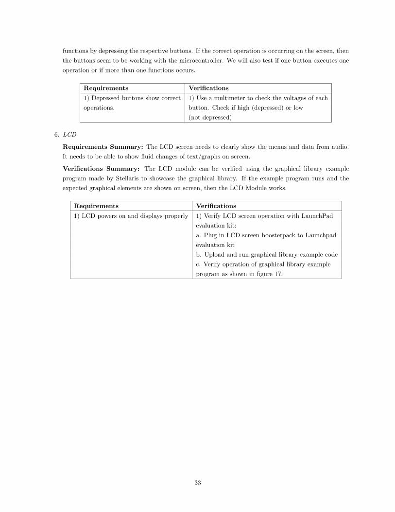
functions by depressing the respective buttons. If the correct operation is occurring on the screen, then
the buttons seem to be working with the microcontroller. We will also test if one button executes one
operation or if more than one functions occurs.
Requirements Verifications
1) Depressed buttons show correct 1) Use a multimeter to check the voltages of each
operations. button. Check if high (depressed) or low
(not depressed)
6. LCD
Requirements Summary: The LCD screen needs to clearly show the menus and data from audio.
It needs to be able to show fluid changes of text/graphs on screen.
Verifications Summary: The LCD module can be verified using the graphical library example
program made by Stellaris to showcase the graphical library. If the example program runs and the
expected graphical elements are shown on screen, then the LCD Module works.
Requirements Verifications
1) LCD powers on and displays properly 1) Verify LCD screen operation with LaunchPad
evaluation kit:
a. Plug in LCD screen boosterpack to Launchpad
evaluation kit
b. Upload and run graphical library example code
c. Verify operation of graphical library example
program as shown in figure 17.
33
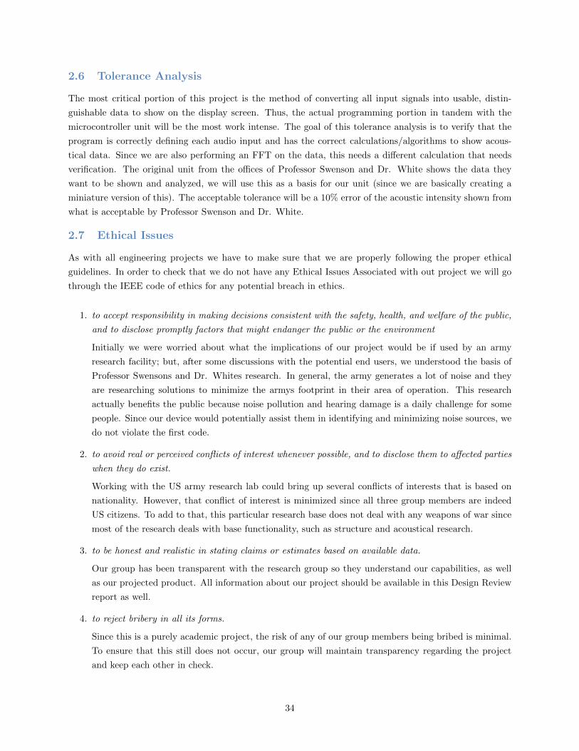
2.6 Tolerance Analysis
The most critical portion of this project is the method of converting all input signals into usable, distin-
guishable data to show on the display screen. Thus, the actual programming portion in tandem with the
microcontroller unit will be the most work intense. The goal of this tolerance analysis is to verify that the
program is correctly defining each audio input and has the correct calculations/algorithms to show acous-
tical data. Since we are also performing an FFT on the data, this needs a different calculation that needs
verification. The original unit from the offices of Professor Swenson and Dr. White shows the data they
want to be shown and analyzed, we will use this as a basis for our unit (since we are basically creating a
miniature version of this). The acceptable tolerance will be a 10% error of the acoustic intensity shown from
what is acceptable by Professor Swenson and Dr. White.
2.7 Ethical Issues
As with all engineering projects we have to make sure that we are properly following the proper ethical
guidelines. In order to check that we do not have any Ethical Issues Associated with out project we will go
through the IEEE code of ethics for any potential breach in ethics.
1. to accept responsibility in making decisions consistent with the safety, health, and welfare of the public,
and to disclose promptly factors that might endanger the public or the environment
Initially we were worried about what the implications of our project would be if used by an army
research facility; but, after some discussions with the potential end users, we understood the basis of
Professor Swensons and Dr. Whites research. In general, the army generates a lot of noise and they
are researching solutions to minimize the armys footprint in their area of operation. This research
actually benefits the public because noise pollution and hearing damage is a daily challenge for some
people. Since our device would potentially assist them in identifying and minimizing noise sources, we
do not violate the first code.
2. to avoid real or perceived conflicts of interest whenever possible, and to disclose them to affected parties
when they do exist.
Working with the US army research lab could bring up several conflicts of interests that is based on
nationality. However, that conflict of interest is minimized since all three group members are indeed
US citizens. To add to that, this particular research base does not deal with any weapons of war since
most of the research deals with base functionality, such as structure and acoustical research.
3. to be honest and realistic in stating claims or estimates based on available data.
Our group has been transparent with the research group so they understand our capabilities, as well
as our projected product. All information about our project should be available in this Design Review
report as well.
4. to reject bribery in all its forms.
Since this is a purely academic project, the risk of any of our group members being bribed is minimal.
To ensure that this still does not occur, our group will maintain transparency regarding the project
and keep each other in check.
34
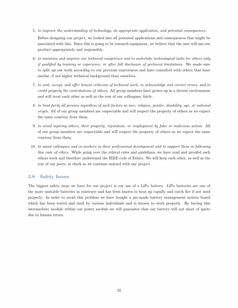
5. to improve the understanding of technology; its appropriate application, and potential consequences.
Before designing our project, we looked into all potential applications and consequences that might be
associated with this. Since this is going to be research equipment, we believe that the user will use our
product appropriately and responsibly.
6. to maintain and improve our technical competence and to undertake technological tasks for others only
if qualified by training or experience, or after full disclosure of pertinent limitations. We made sure
to split up our work according to our previous experiences and have consulted with others that have
similar, if not higher technical background than ourselves.
7. to seek, accept, and offer honest criticism of technical work, to acknowledge and correct errors, and to
credit properly the contributions of others. All group members have grown up in a diverse environment
and will treat each other as well as the rest of our colleagues, fairly.
8. to treat fairly all persons regardless of such factors as race, religion, gender, disability, age, or national
origin. All of our group members are respectable and will respect the property of others as we expect
the same courtesy from them.
9. to avoid injuring others, their property, reputation, or employment by false or malicious action. All
of our group members are respectable and will respect the property of others as we expect the same
courtesy from them.
10. to assist colleagues and co-workers in their professional development and to support them in following
this code of ethics. While going over the ethical rules and guidelines, we have read and proofed each
others work and therefore understand the IEEE code of Ethics. We will keep each other, as well as the
rest of our peers, in check as we continue onward with our project.
2.8 Safety Issues
The biggest safety issue we have for our project is our use of a LiPo battery. LiPo batteries are one of
the more unstable batteries in existence and has been known to heat up rapidly and catch fire if not used
properly. In order to avoid this problem we have bought a pre-made battery management system board
which has been tested and used by various individuals and is known to work properly. By having this
intermediate module within our power module we will guarantee that our battery will not short of ignite
due to human errors.
35
3 Cost and Schedule
3.1 Cost Analysis
Table 2: Labor
Member Hourly rate Total hours Subtotal x 2.5
Kristine Cabrera $35 130 $11375
Kevin Chen $35 130 $11375
Joseph Shim $35 130 $11375
Total $34125
Table 3: Parts
Parts Quantity Cost per Unit Total Order Status
Stellaris LM4F120 1 $12.99 $12.99 Ordered
KS0108 LCD display 2 $35.00 $70.00 Ordered
5V/1A Wall Adapter 1 $5.95 $ 5.95 Ordered
USB/DC LiPo Battery 1 $17.95 $17.95 Ordered
Charger
Polymer Li-Ion Bat 1 $11.95 $11.95 Ordered
2600 mAh
USB 2.0 Cable 1 $0.85 $0.85 Have
Voltage Regulator 2 $1.95 $3.90 ECE Shop
LM317
Synchronous Boost 1 $4.95 $4.95 Ordered
Converter - TPS61070
PCM1801 ADC 3 $6.97 $20.91 Ordered
PLL1705 Clock Chip 2 $4.03 $8.06 Ordered
OPA227PA Op-Amp 5 $0.643 $3.22 Ordered
PCB 2 $0.00 $0.00 Need to Design
LEDs 10 $0.262 $2.62 ECE Store
RCL Components N/A $0.00 $0.00 ECE Service
Shop
LiPo Battery 1 $22.50 $22.50 Ordered
Mic Probe 1 $0.00 $0.00 At CERL
BNC Connectors 3 $5.57 $16.71 ECE Store
Pushbuttons 10 $3.06 $30.60 ECE Service
Shop
Total $232.31
36
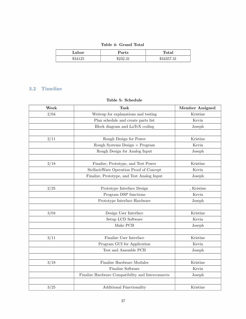
Table 4: Grand Total
Labor Parts Total
$34125 $232.31 $34357.31
3.2 Timeline
Table 5: Schedule
Week Task Member Assigned
2/04 Writeup for explanations and testing Kristine
Plan schedule and create parts list Kevin
Block diagram and LaTeX coding Joseph
2/11 Rough Design for Power Kristine
Rough Systems Design + Program Kevin
Rough Design for Analog Input Joseph
2/18 Finalize, Prototype, and Test Power Kristine
StellarisWare Operation Proof of Concept Kevin
Finalize, Prototype, and Test Analog Input Joseph
2/25 Prototype Interface Design , Kristine
Program DSP functions Kevin
Prototype Interface Hardware Joseph
3/04 Design User Interface Kristine
Setup LCD Software Kevin
Make PCB Joseph
3/11 Finalize User Interface Kristine
Program GUI for Application Kevin
Test and Assemble PCB Joseph
3/18 Finalize Hardware Modules Kristine
Finalize Software Kevin
Finalize Hardware Compatibility and Interconnects Joseph
3/25 Additional Functionality Kristine
37
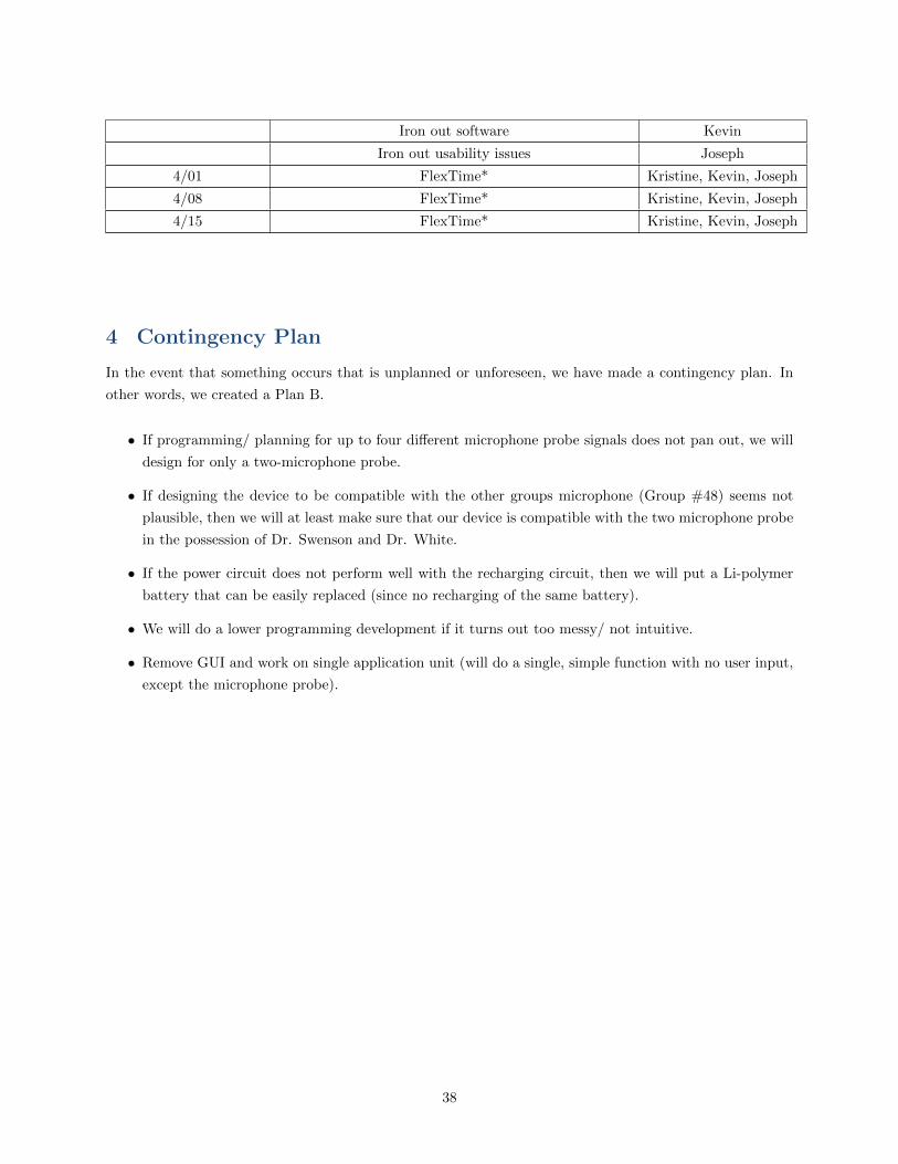
Iron out software Kevin
Iron out usability issues Joseph
4/01 FlexTime* Kristine, Kevin, Joseph
4/08 FlexTime* Kristine, Kevin, Joseph
4/15 FlexTime* Kristine, Kevin, Joseph
4 Contingency Plan
In the event that something occurs that is unplanned or unforeseen, we have made a contingency plan. In
other words, we created a Plan B.
• If programming/ planning for up to four different microphone probe signals does not pan out, we will
design for only a two-microphone probe.
• If designing the device to be compatible with the other groups microphone (Group #48) seems not
plausible, then we will at least make sure that our device is compatible with the two microphone probe
in the possession of Dr. Swenson and Dr. White.
• If the power circuit does not perform well with the recharging circuit, then we will put a Li-polymer
battery that can be easily replaced (since no recharging of the same battery).
• We will do a lower programming development if it turns out too messy/ not intuitive.
• Remove GUI and work on single application unit (will do a single, simple function with no user input,
except the microphone probe).
38
5 References
1. ”LM317.” Texas Instruments. Texas Instruments, n.d. Web. 22 Feb 2013.
http://www.ti.com/lit/ds/symlink/lm317.pdf
2. TPS61070.” Texas Instruments. Texas Instruments, n.d. Web. 23 Feb 2013.
http://www.ti.com/lit/ds/symlink/tps61070.pdf
3. ”USB/DC Lithium Polymer battery charger.” Adafruit. Adafruit. Web. 23 Feb 2013.
https://www.adafruit.com/products/280
4. Stellaris LM4F120 LaunchPad Evaluation Board User Manual, Austin, TX, 2010. [Online].
http://www.ti.com/litv/pdf/spmu289a
5. Stellaris LaunchPad LCD Boosterpack EB-LM4F120-L35 Users Guide, Futian District, Shenzhen,
PRC. [Online].
http://www.kentecdisplay.com/uploads/soft/Products spec/EB-LM4F120-L35 UserGuide 04.pdf
6. Single-Ended Analog-Input 16-Bit Stereo Analog-to-Digital Converter, Dallas, TX, 2007. [Online].
http://www.mouser.com/ds/2/405/sbas131c-114090.pdf
7. Stellaris LM4F120H5QR Microcontroller Data Sheet, Austin, TX, 2013. [Online].
http://www.ti.com/lit/gpn/lm4f120h5qr
8. Stellaris Peripheral Driver Library Users Guide, Austin, TX, 2012. [Online]
http://www.ti.com/general/docs/lit/getliterature.tsp?literatureNumber=spmu019o&fileType=pdf
9. Stellaris Graphics Library Users Guide, Austin, TX, 2012. [Online]
http://www.ti.com/general/docs/lit/getliterature.tsp?literatureNumber=spmu018o&fileType=pdf
10. Dual-SPI Emulating I2S on Stellaris LM4F MCUs, Austin, TX, 2012. [Online]
http://www.ti.com/general/docs/lit/getliterature.tsp?literatureNumber=spma042a&fileType=pdf
39