Embed Size (px)
Citation preview
Acoustooptic techniques for comparing high-speeddigital data
Anastasios P. Goutzoulis and Peter J. Chantry
The possibility of using acoustooptic techniques for recording and comparing high-speed digital data isexplored. Suitable architectures for high-speed acoustooptic (AO) comparators capable of determining theoccurrence, nature, and location of errors are presented. The analysis indicates that the AO Bragg cell must
have a minimum center frequency of twice the data clock frequency and a minimum bandwidth equal to theclock frequency. Initial experimental results verify the analysis and demonstrate the feasibility of theproposed techniques at clock frequencies of at least 330 MHz. Available AO technology should allow the
application of this approach at clock frequencies in excess of 1 GHz.
1. Introduction
Acoustooptic techniques have been successfully ap-plied to various areas of signal processing such as spec-trum analysis1 and ambiguity processing.2 This ispartially due to the inherent properties of optics whichallow for fast parallel 2-D operations. It is also due tothe capability of Bragg cells to operate as high-fre-quency high-capacity (i.e., large time-bandwidthproduct) optically accessed analog shift registers. Assuch, these devices are well suited for applicationswhere one needs to operate over long streams of high-bandwidth data.
One such application involves comparison of long-duration high-bandwidth digital data. This is a rela-tively new area of signal processing and is largely cou-pled with the interest for the testing of high-speedand/or high-density digital integrated circuits (e.g.,GaAs and VHSIC). Part of the testing involves com-parison of the chip output and the expected referenceoutput. The chip output usually involves a number ofoutput channels. The output signal has a digital for-mat and a clock frequency that can reach several hun-dreds of megahertz. The tester of such devices shouldbe capable of providing information about (a) occur-rence of errors, (b) nature of errors (e.g., logic 0 insteadof 1), and (c) location of errors in terms of output stateand channel. It should also be able to perform a fast
The authors are with Westinghouse R&D Center, 1310 BeulahRoad, Pittsburgh, Pennsylvania 15235.
Received 19 August 1985.0003-6935/86/060933-07$02.00/0.© 1986 Optical Society of America.
parallel comparison for a large number of serial inputbits [e.g., several megabytes (MB)] over many parallelchannels (e.g., >32). In many cases, the comparisonneeds to be performed in real time.
The above comparison requirements could be metvia the use of digital technology. Possible problemsassociated with this approach are the need for large-capacity high-speed shift registers and memory, de-gree of achievable parallelism, and particularly therequirement of higher clock frequencies (i.e., >500MHz). Acoustooptic (AO) processors with their in-herently high speed offer an alternative technologicalapproach which we explore in the present paper.
In Sec. II we briefly state the digital data comparisonproblem. Various AO architectures are then de-scribed in Sec. III. Theoretical considerations rele-vant to the processor performance are then detailed inSec. IV. In Sec. V we present some initial experimen-tal data. Section VI is a summary and conclusions.
11. Comparison of High-Speed Digital Data
High-speed digital data are usually provided fromhigh-speed VLSI devices. Currently available typicalVLSI chips can operate at clock frequencies of •100MHz and have 32-64 output channels. Future GaAsVLSI devices are expected to have more than 32 out-put channels and clock frequencies well above 700MHz. In most cases, the data rate is half of the clockfrequency. A logic 1 is represented by a high level heldfor a single clock period with return-to-zero (RZ) oc-curring for the following clock period. Logic 0 is repre-sented by two successive clock periods at the zero orlow level.
The objective of data comparison is to determinewhether for a given input signal (usually called inputvector since it is a set of parallel input bits) the chip
15 March 1986 / Vol. 25, No. 6 / APPLIED OPTICS 933
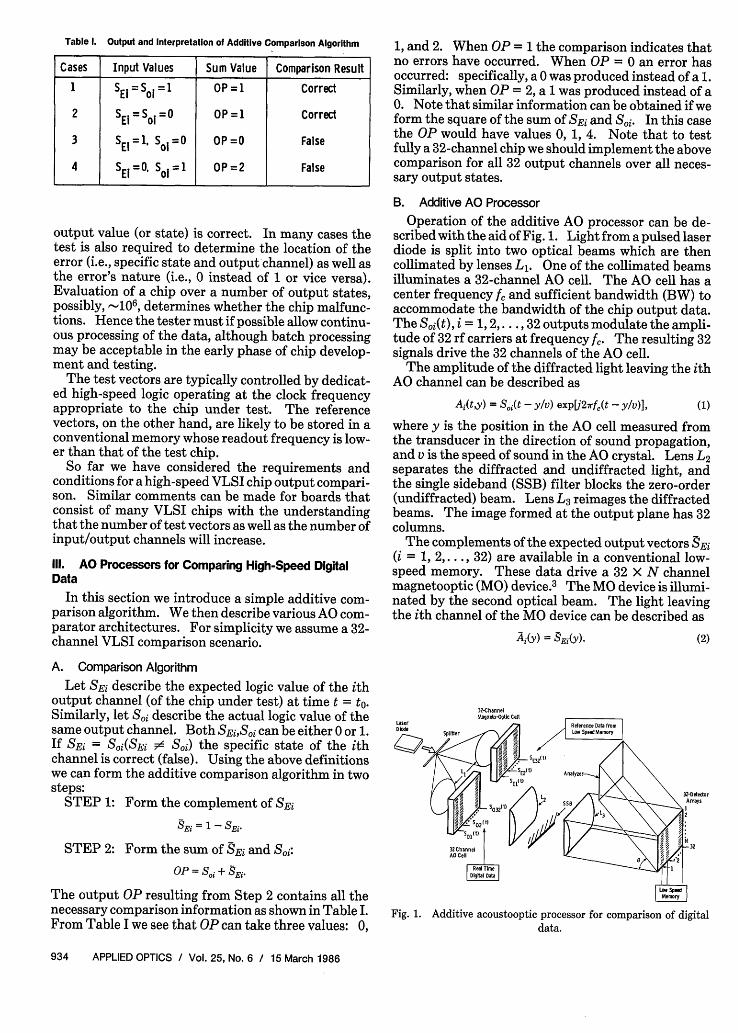
Table I. Output and Interpretation of Additive Comparison Algorithm
Cases Input Values Sum Value Comparison Result
1 SEl =1 = 1 OP=1 Correct
2 SEl = Sol =o 0P=1 Correct
3 SEl = 1 S =O OP =O False
4 SE = S = I OP = 2 False
output value (or state) is correct. In many cases thetest is also required to determine the location of theerror (i.e., specific state and output channel) as well asthe error's nature (i.e., 0 instead of 1 or vice versa).Evaluation of a chip over a number of output states,possibly, -106, determines whether the chip malfunc-tions. Hence the tester must if possible allow continu-ous processing of the data, although batch processingmay be acceptable in the early phase of chip develop-ment and testing.
The test vectors are typically controlled by dedicat-ed high-speed logic operating at the clock frequencyappropriate to the chip under test. The referencevectors, on the other hand, are likely to be stored in aconventional memory whose readout frequency is low-er than that of the test chip.
So far we have considered the requirements andconditions for a high-speed VLSI chip output compari-son. Similar comments can be made for boards thatconsist of many VLSI chips with the understandingthat the number of test vectors as well as the number ofinput/output channels will increase.
Ill. AO Processors for Comparing High-Speed DigitalData
In this section we introduce a simple additive com-parison algorithm. We then describe various AO com-parator architectures. For simplicity we assume a 32-channel VLSI comparison scenario.
A. Comparison Algorithm
Let Ei describe the expected logic value of the ithoutput channel (of the chip under test) at time t = to.Similarly, let Si describe the actual logic value of thesame output channel. Both SEiSi can be either 0 or 1.If SE = Soi(SEi S) the specific state of the ithchannel is correct (false). Using the above definitionswe can form the additive comparison algorithm in twosteps:
STEP 1: Form the complement of Ei
SEi = 1 - SEi-
STEP 2: Form the sum of SEi and Si:
OP = S + SEi-
The output OP resulting from Step 2 contains all thenecessary comparison information as shown in Table I.From Table I we see that OP can take three values: 0,
1, and 2. When OP = 1 the comparison indicates thatno errors have occurred. When OP = 0 an error hasoccurred: specifically, a 0 was produced instead of a 1.Similarly, when OP = 2, a 1 was produced instead of a0. Note that similar information can be obtained if weform the square of the sum of SEi and Si. In this casethe OP would have values 0, 1, 4. Note that to testfully a 32-channel chip we should implement the abovecomparison for all 32 output channels over all neces-sary output states.
B. Additive AO Processor
Operation of the additive AO processor can be de-scribed with the aid of Fig. 1. Light from a pulsed laserdiode is split into two optical beams which are thencollimated by lenses L1. One of the collimated beamsilluminates a 32-channel AO cell. The AO cell has acenter frequency f and sufficient bandwidth (BW) toaccommodate the bandwidth of the chip output data.The S0i(t), i = 1, 2,..., 32 outputs modulate the ampli-tude of 32 rf carriers at frequency f. The resulting 32signals drive the 32 channels of the AO cell.
The amplitude of the diffracted light leaving the ithAO channel can be described as
Ai(t,y) = S(t - y/v) expU27rf,(t -yv)], (1)
where y is the position in the AO cell measured fromthe transducer in the direction of sound propagation,and v is the speed of sound in the AO crystal. Lens L2separates the diffracted and undiffracted light, andthe single sideband (SSB) filter blocks the zero-order(undiffracted) beam. Lens L3 reimages the diffractedbeams. The image formed at the output plane has 32columns.
The complements of the expected output vectors SEi(i = 1, 2,..., 32) are available in a conventional low-speed memory. These data drive a 32 X N channelmagnetooptic (MO) device. 3 The MO device is illumi-nated by the second optical beam. The light leavingthe ith channel of the MO device can be described as
Ai(y) = SEi(y). (2)
32-ChannelMagneo-Opti Cel
tLaserDtodeL-
32-DetorArrays
Fig. 1. Additive acoustooptic processor for comparison of digitaldata.
934 APPLIED OPTICS / Vol. 25, No. 6 / 15 March 1986
This image has also 32 columns. Note that in writingEqs. (1) and (2) we have assumed that the AO cell andMO device have equal efficiencies which we have setarbitrarily to unity.
The AO cell, MO device, and the rest of the opticalsystem are arranged so that the two 32-column outputimage beams have equal intensities and interfere at the32 detector arrays. The arrangement is so that the ithcolumn of the AO cell image coincides with the ithcolumn of the MO device image. This can be achievedif the MO and AO devices' images are of equal dimen-sions. Under these conditions the total intensity dfthe ith column of the output image so formed is
Ii(t,xi,y) = IA(t,y) + Ai(y) exp(j2irrx)j 2
= IS(t - Y/)1 + ISEi(y)l
+ 2S0 i(t - y/v)SEj(y) exp(-j2rrxj), (3)
where xi denotes the location in the x-directionof the center of the ith column. The phase factorexp(-j27rrxi) arises from the angular separation 0 ofthe optical beams, where r = sin 0/A, and X is the laserwavelength. Assuming that the spacing of the 32 AOcell/MO device channels is uniform and such that thearguments rxi of the phase factor form an integer pro-gression, Eq. (3) can be written as
I(t,y) =1S0 (t -ylV)1 2 + SEi(y)l + KS(t-y/v)SEi(y), (4)
where K is a constant whose range needs to be 0 < K <1. Note that in writing Eq. (4) we assumed that thewidth of each image column is small compared to thewavelength of the spatial carrier [third term in Eq. (3)].This can be achieved by using narrow AO cell/MOdevice channels, small tilt, etc. Note that the ideabehind the above requirements is to obtain a construc-tive phase weighting that is the same for each of the 32final image columns. This is not a necessary require-ment, but it does simplify the required postprocessingconsiderably.
As mentioned, the laser diode is operating in apulsed mode. The laser pulse width is TL, and thepulse period is T so that
T 2 NTb = TA, (5)
where Tb is the bit period, TA is the AO cell timeaperture, and N = TA/Tb is the number of bits oroutput states present in each of the 32 columns of theAO cell. Note that N is also the number of expectedoutput vectors present in each of the 32 channels of theMO device. The laser pulse width TL is kept so thatTL < Tb/2, so that while the laser pulse is on there is nosignificant motion of the data present in the AO cell.
Since the data are frozen while the pulse is on, theinformation written on the jth detector pixel of the ithcolumn can be described as
I,(yj) = IS,(yj)l2 + IEi(yj)2 + 2KSj(yj)3Ej(yj)
j Soij + SEij + 2KSogjSEije (6)
where yj, I = 1, 2,. . ., N represents the spatial locationof the jth detector pixel. The above equation can be
further simplified if one drops the squares becauseSoijSEii can take only the values of 0 or 1. In this caseEq. (6) can be written as
Iij = Soij + Eij + 2KSijEij. (7)
Equation (7) contains complete information aboutpossible errors that occurred in the jth state of the ithoutput channel. To see this, consider the case of K =0, when
oij = Sij + SEij (8)
As can be seen from Eq. (8), Iij is exactly the desiredtest output OP described in Step 2. Note that for theextreme case of K = 1 the output has the form
Iij = Soij + SEij + 2 SoijSEij' (9)
which is equivalent to forming the square of the outputOP. Also note that for any other value of K, 0 < K < 1,the three possible values of OP are 0, 1, and 2 + 2K.
In conclusion we see that the optical architecture ofFig. 1 is capable of providing complete comparisonresults for N serial states of the 32 output channels.Note that the system described can also operate in anoncoherent mode. In this mode we may use two laserdiodes, one for the AO cell and one for the MO device.In this case a simple analysis shows that the detectoroutput is given by Eq. (8).
C. AO Processors for Different Comparison Scenarios
As we showed in Sec. III.B, the AO processor of Fig. 1is capable of fully comparing N states of the full 32-channel output per laser shot. This particular archi-tecture employs a 2-D magnetooptic device which hasthe property of being addressable at moderate speedand then holding the information fixed in both timeand space until readdressed. Hence the reference op-tical channel can be operated by a moderate speedconventional memory which contains the expectedoutputs. For this scenario, the data comparison re-quires batch processing.
The comparison speed of the above architecture islimited by the speed of the slowest device. Let usassume that a 32 X 256 parallel addressed 10-MHzclock frequency MO device is available. In this case,we need 25.6 As to load 32 vectors (256 bits deep).Note that the same amount of information can beloaded into the AO cell much faster. For example, for800-MHz clock frequency chip data, the loading timeis 0.64 As. Consider now the readout time of the detec-tor array. Using 4 detector pixels/output bit, we needa total of 1024 pixels. For a 16 readout channel, 16-MHz readout frequency detector array, the readouttime is 8 As. Thus, for this scenario, the comparisonspeed is 25.6 As and is set by the MO device.
Let us now assume that the reference expected out-put vectors are available at the speed with which we areprovided the actual chip data. For this scenario thecomparison speed can be improved by replacing theMO device with a second AO cell. For this system, thecomparison time required is 8 Ms with the limitingfactor being the output detector array. Further im-
15 March 1986 / Vol. 25, No. 6 / APPLIED OPTICS 935
provement in speed requires use of faster detectorarrays.
Note that in another possible scenario, one can elim-inate completely the top part (i.e., MO device arm) ofthe optical system of Fig. 1. In this case the detectoroutputs correspond to an image of the N logic states(present in the AO cell) and take values of 0 or 1. Thusthe optics are used to record (or capture) N states perchannel. The comparison is subsequently done elec-tronically on line at the detector outputs. In this casethe comparison time is 8 Ms. This technique offers themaximum possible comparison speed, while it elimi-nates the need for a high-speed reference source.This, however, is achieved at the expense of consider-able electronic postprocessing.
IV. Component Requirements
As noted in Sec. III.B the digital data under compar-ison must be applied as modulation of a carrier (whosefrequency is equal to the cell's center frequency). Tosatisfy the Nyquist sampling requirements we need atleast 2 carrier cycles/bit, and thus the Bragg cell'scenter frequency needs to be at least twice the clockfrequency. The cell's required BW can be determinedby considering a single 1 bit represented by a singlesquare pulse of duration Tb/2. The Fourier transformof this is a sinc function centered at f = f with a mainlobe width of 4/Tb or twice the clock frequency. Themain lobe contains over 80% for the signal energy while50% of the energy is contained within ft + 1/Tb or over abandwidth of 2/Tb = f/2. The latter is an acceptablefigure since it can be easily satisfied with state-of-the-art Bragg cells.
The Bragg cell's time-bandwidth product (TBW) isdetermined by the number of detector pixels available.For example, if 1024 pixels are available and we allo-cate 4 pixels/tested (or recorded) bit, we need a TBWof 512. This implies that the data are compared at arate of 256 bits/laser shot-AO channel. Note, howev-er, that for high-bandwidth data such rates are notalways achievable because of AO materials limitations.
To consider the laser diode requirements, we need toperform a simple light budget, analysis. For purposesof this analysis, we assume that a single-laser diodeilluminates a single AO channel which is then imagedonto a single K-element detector array. Each pixelhas a width W and height H. With the detector satu-ration exposure being SE (joules/unit area), we findthat the total saturation energy required is
S = SE X K X W X H (joules). (10)
The total laser energy per pulse is
EL = TL X P (joules), (11)
where P is the average laser power while on in watts.Assuming an AO diffraction efficiency of nAO and anoptical system transmission efficiency of no, we findthat the total laser pulse energy reaching the detectoris
ET =ELX nAO X nO. (12)
From Eq. (12) and (10) we calculate the achievablefraction of detector saturation:
SI ET ELX nAO X nO (13)
S SEXKx WXHLet us now consider an example of the above analysis
in conjunction with a specific recording scenario simi-lar to the last case of Sec. III.C. We assume data of500-MHz clock frequency and a 128-bit/shot AO chan-nel recording rate. We will use a Reticon CCPD 128 X4 detector array because of its fast readout (125 kHz).For this array K = 512, W = H = 18 Am, and SE = 1 X10⁻⁶ J/cm 2 , thus S = 1.66 X 10⁻⁹ J. To record thedigital data without significant output smearing weuse a laser pulse of 2 ns. Furthermore, we assume anoptical system with no = 0.5. In this case
ET = 2 X 10⁹ X P X 0.5 X nAO. (14)
The detector array has a dynamic range of -400:1.This is well above the needs of this present application,where we are concerned only with digital information,and the required dynamic range depends on the pre-scribed probability of an error. Assuming a standarddeviation about the 0 level of 1/400 of saturation andthat a probability of -10-12 is prescribed for a 0 beingrecorded as a 1, the threshold separating 0 and 1 signalsmust be set at -8/400 of saturation. If the 1 signallevel is derived from a laser having pulse-to-pulse fluc-tuations of - + 10%, an approximately equal probabili-ty will exist for recording a 1 as a 0 if the mean 1 signallevel is 30/400 of saturation. To achieve this the avail-able diffracted laser energy must be sufficient to make
SI = = 0.075.400
(15)
From Eq. (12), (13), and (14) we can now calculate thepulsed laser power P needed for three different AO celldiffraction efficiencies: P = 1.25 W (nAO = 0.1); P =0.63 W (nAO = 0.2), and P = 0.42 W (nAO = 0.3). Fromthese numbers we can conclude that, for the specificscenario we considered, the laser power requirement iseasily satisfied by readily available laser diodes.
The above analysis has considered a single laserdiode per AO cell channel. To calculate the pulsedlaser power required for an M-channel cell, we have tomultiply the above numbers by 2 X M, where theadditional factor of -2 represents the wasted light dueto the spacing between adjacent AO channels. Forexample, with M = 32 the laser power required is P =80 W (nAO = 0.1), 40.3 W (nAO = 0.2), and 26.9 W (nAO =0.3). These laser powers are considerably higher butcould still be satisfied by existing technology. Howev-er, for the laser to match the speed capabilities of theassumed readout device it needs to operate at 125-kHzprf. For the M-channel case considered here this prfmay not be possible with an existing laser, which thenbecomes the slowest device in the recording scenario.
From the above brief discussion, we can concludethat currently available state-of-the-art technologycan satisfy the component requirements needed forthe comparison or recording of high-speed digital data.For most realistic scenarios, however, one would haveto consider trade-offs of hardware and speed.
936 APPLIED OPTICS / Vol. 25, No. 6 / 15 March 1986
AO SSBCell C S Filter
Laser 'Diode I
50mm
Filter 400 m
Fig. 2. Experimental system.
V. Experimental Results
In the first part of our experimental work we ad-dressed the problem of data acquisition, that is, read-out of the detector array which has been exposed to thedata present in a single-channel Bragg cell. We firstbuilt the top part of the AO processor of Fig. 2.
The available laser diode had a peak power of <5mW and pulse widths varied between 2 and 7 ns. Tocompensate for the lack of peak power it was necessaryto pulse the laser diode many times (laser prf 10MHz) per detector readout. This technique, however,requires that the exact same signal (e.g., a pulse train)be present in the AO cell every time a new laser pulse ison. This was conveniently achieved by using a squarewave pulse train to modulate the AO cell and derivingfrom this a synchronized train of laser trigger pulses ata subharmonic prf. In general, the square waves had aduty cycle of 50%, thereby simulating a string of digitaldata of logic value 1 at an equivalent clock frequencygiven by the reciprocal of the pulse width. We consis-tently use this definition of the equivalent clock fre-quency including those cases where we have operatedat <50% duty cycle.
The detector array was a Reticon RL-1024s arraywith H = 2.5 mm, W = 25 m, and SE = 50 X 10-9J/cm2. The readout clock frequency is 300 kHz, whichcorresponds to a minimum integration time of 3.44 msinvolving 3.4 X 10⁴ laser pulses.
We first used a PbMoG 4 Bragg cell with ft = 312MHz, BW = 150 MHz, and nAO = 0.003. The usableaperture was 2MAs (-8 mm) and a corresponding TBWof -300.
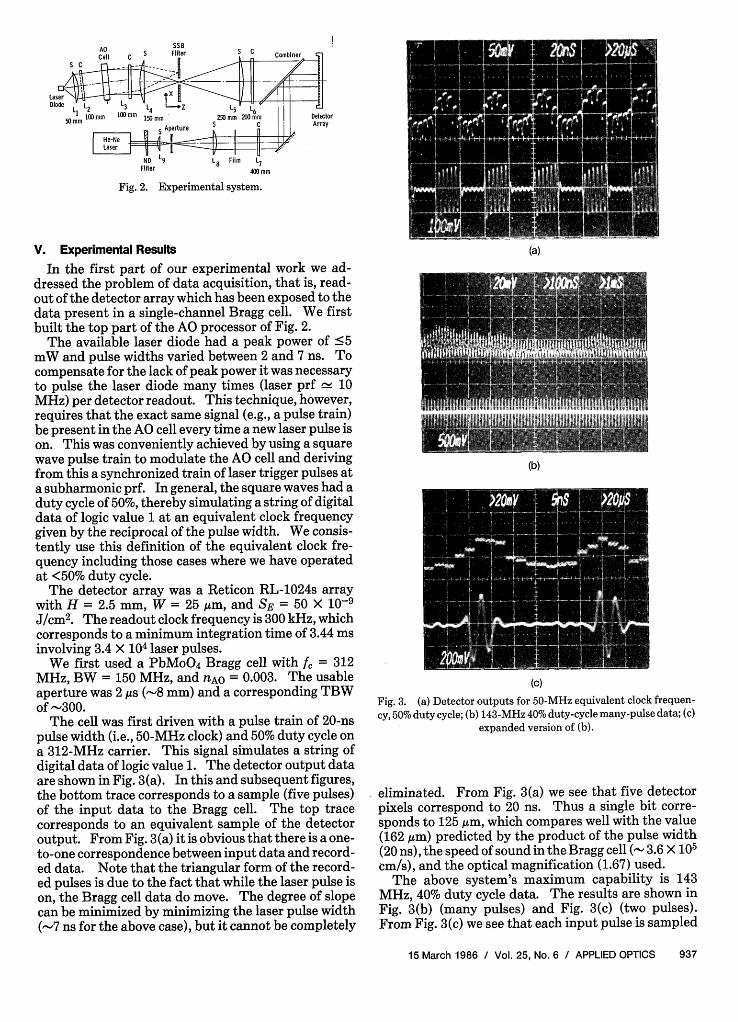
The cell was first driven with a pulse train of 20-nspulse width (i.e., 50-MHz clock) and 50% duty cycle ona 312-MHz carrier. This signal simulates a string ofdigital data of logic value 1. The detector output dataare shown in Fig. 3(a). In this and subsequent figures,the bottom trace corresponds to a sample (five pulses)of the input data to the Bragg cell. The top tracecorresponds to an equivalent sample of the detectoroutput. From Fig.3(a) itis obvious that there is a one-to-one correspondence between input data and record-ed data. Note that the triangular form of the record-ed pulses is due to the fact that while the laser pulse ison, the Bragg cell data do move. The degree of slopecan be minimized by minimizing the laser pulse width(-7 ns for the above case), but it cannot be completely
(a)
(b)
(c)
Fig. 3. (a) Detector outputs for 50-MHz equivalent clock frequen-cy, 50% duty cycle; (b) 143-MHz 40% duty-cycle many-pulse data; (c)
expanded version of (b).
eliminated. From Fig. 3(a) we see that five detectorpixels correspond to 20 ns. Thus a single bit corre-sponds to 125 Mm, which compares well with the value(162 Am) predicted by the product of the pulse width(20 ns), the speed of sound in the Bragg cell (" 3.6 X 105cm/s), and the optical magnification (1.67) used.
The above system's maximum capability is 143MHz, 40% duty cycle data. The results are shown inFig. 3(b) (many pulses) and Fig. 3(c) (two pulses).From Fig. 3(c) we see that each input pulse is sampled
15 March 1986 / Vol. 25, No. 6 / APPLIED OPTICS 937
(a)
,4
(b)
Fig.4. (a) Detector outputs for 210-MHz equivalent clock frequen-cy, 50% duty cycle data; (b) 330-MHz equivalent clock frequency,
35% duty cycle data.
by -2.5 cycles of carrier. For all practical purposesthis was found to be the minimum possible acceptablesampling rate. Note that the envelope seen in Fig.3(b) is due to spatial nonuniformities of the laser beam.Also note that for this experiment lens L4 had a focallength of 80 mm.
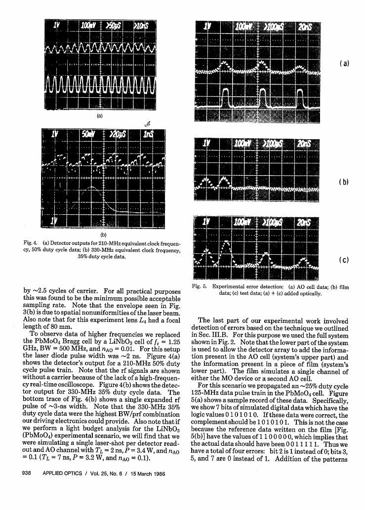
To observe data of higher frequencies we replacedthe PbMoO 4 Bragg cell by a LiNbO 3 cell of f = 1.25QHz, BW = 500 MHz, and nAO = 0.01. For this setupthe laser diode pulse width was -2 ns. Figure 4(a)shows the detector's output for a 210-MHz 50% dutycycle pulse train. Note that the rf signals are shownwithout a carrier because of the lack of a high-frequen-cy real-time oscilloscope. Figure 4(b) shows the detec-tor output for 330-MHz 35% duty cycle data. Thebottom trace of Fig. 4(b) shows a single expanded rfpulse of -3-ns width. Note that the 330-MHz 35%duty cycle data were the highest BW/prf combinationour driving electronics could provide. Also note that ifwe perform a light budget analysis for the LiNbO3(PbMoO4 ) experimental scenario, we will find that wewere simulating a single laser-shot per detector read-out and AO channel with TL = 2 ns, P = 3.4 W, and nAO= 0.1 (TL = 7ns,P= 3.2 W,andnAo = 0.1).
* E i alm l ol (a)
- m~~~omsmn_
Fig. 5. Experimental~ ~ ero deetin (a.A.clldaa;(b.fl
data; c)tes dd y.
The last part of our experimental work involveddetection of errors based on the technique we outlinedin Sec. III.B. For this purpose we used the full systemshown in Fig. 2. Note that the lower part of the systemis used to allow the detector array to add the informa-tion present in the A cell (system's upper part) andthe information present in a piece of film (system'slower part). The film simulates a single channel ofeither the MO device or a second A cell.
For this scenario we propagated an -25% duty cycle125-MHz data pulse train in the PbMoG4 cell. Figure5(a) shows asample record of these data. Specifically,we show 7 bits of simulated digital data which have thelogic values 0 1 0 1 0 1 0. If these data were correct, thecomplement should be 0 10 101. This is not the casebecause the reference data written on the film [Fig.5(b)J have the values of 1 1 00 0 00, which implies thatthe actual data should have been 0 01 1 1 1 1. Thus wehave a total of four errors: bit 2 is 1 instead of 0; bits 3,5, and 7 are 0 instead of 1. Addition of the patterns
938 APPLIED OPTICS / Vol. 25, No. 6 / 15 March 1986
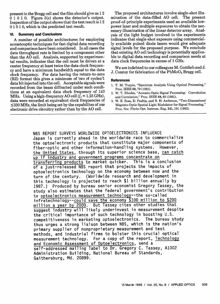
present in the Bragg cell and the film should give us 1 20 1 0 1 0. Figure 5(c) shows the detector's output.Inspection of the output shows that the test result is 1 20 1 0 1 0, which is the predicted test result.
VI. Summary and Conclusions
A number of possible architectures for employingacoustooptic techniques for fast digital data recordingand comparison have been considered. In all cases thedata throughput rate is limited by a component otherthan the AO cell. Analysis, supported by experimen-tal results, indicates that the cell must be driven at acenter frequency at least twice the data clock frequen-cy and have a minimum bandwidth equal to the dataclock frequency. For data having the return-to-zero(RZ) format this gives a minimum of two rf cycles/1data bit injected into the cell. Acceptable signals wererecorded from the beam diffracted under such condi-tions at an equivalent data clock frequency of 143MHz. Usingahigh-frequencyAOcell(ft= 1.25GHz),data were recorded at equivalent clock frequencies of•330 MHz, the limit being set by the capabilites of ourelectronic drive circuitry rather than by the AO cell.
The proposed architectures involve single-shot illu-mination of the data-filled AO cell. The presentproof-of-principle experiments used an available low-power laser and multiple exposures to obtain the nec-essary illumination of the linear detector array. Anal-ysis of the light budget involved in the experimentsindicates that single-shot exposure using commercial-ly available pulsed diode lasers would give adequatesignal levels for the proposed purpose. We concludethat existing AO cell technology is potentially applica-ble to digital data recording and comparison needs atdata clock frequencies in excess of 1 GHz.
We are indebted to our colleagues M. Gottlieb and J.J. Conroy for fabrication of the PbMoO4 Bragg cell.
References1. T. M. Turpin, "Spectrum Analysis Using Optical Processing,"
Proc. IEEE 69, 79 (1981).2. W. T. Rhodes, "Acousto-Optic Signal Processing: Convolution
and Correlation," Proc. IEEE 69, 65 (1981).3. W. E. Ross, D. Psaltis, and R. H. Anderson, "Two-Dimensional
Magneto-Optic Spatial Light Modulator for Signal Processing,"Proc. Soc. Photo-Opt. Instrum. Eng. 341, 191 (1982).
NBS REPORT SURVEYS WORLDWIDE OPTOELECTRONICS INFLUENCE
Japan is currently ahead in the worldwide race to commercialize
the optoelectronic products that constitute major components of
fiber-optic and other information-handling systems. However,
the United States, through its superior science base, can catch
up if industry and government programs concentrate on
transferring products to market quicker. This is a conclusion
of a just-released NBS report that projects the impacts of
optoelectronics technology on the economy between now and the
turn of the century. (Worldwide research and development in
this technology is projected to reach $1 billion annually by
1987.) Produced by bureau senior economist Gregory Tassey, the
study also estimates that the federal government's contribution
to optoelectronics measurement technology--the so-called
infratechnology--could save the economy 100 million to $200
million a year by 2000. But Tassey cites other studies that
suggest industry will likely underinvest in measurement despite
the critical importance of such technology in boosting U.S.
competitiveness in marketing optoelectronics. The bureau study
thus urges a strong liaison between NBS, which is the nation's
primary supplier of nonproprietary measurement and test
methods, and industrial firms to bolster this crucial optical
measurement technology. For a copy of the report, Technology
and Economic Assessment of Optoelectronics, send a
self-addressed mailing label to Dr. Gregory C. Tassey, A1002
Administration Building, National Bureau of Standards,Gaithersburg, Md. 20899.
15 March 1986 / Vol. 25, No. 6 / APPLIED OPTICS 939


![Anisotropy of the acoustooptic figure of merit for LiNbO3 ...Lithium niobate crystals possess low acoustic attenuation in the high acoustic wave frequency range [5,8], which leads](https://img.pdfslide.net/doc/110x75/600d4960a2e91748bc245e5e/anisotropy-of-the-acoustooptic-figure-of-merit-for-linbo3-lithium-niobate-crystals.jpg)