Embed Size (px)
Citation preview

ACT286130V Buck-Boost Charger with Integrated MOSFETs and
OTG
Data Sheet Rev. E, September 2019 | Subject to change without notice 1 of 94 www.qorvo.com
© 2020 Qorvo US, Inc. All rights reserved.
BENEFITS and FEATURES
• Wide VIN Range: 3.9V to 29V (No Dead Zone)
• Supports 2 to 5 Cell Lithium-ion Batteries
• Supports OTG Function (5V ~ 22.5V Input) with
wide range of output voltages
• OTG output supports QC3.0 / USB PD + PPS output
levels and transition times
• Programmable Frequency: 125KHz, 250KHz,
500kHz, and 1MHz
• 2V ~ 5.1V/100mA Programmable Output LDO
• Precision 0.5% Voltage Reference
• +/-4% Output Constant Current Regulation
• < 5 μA Leakage Current from Battery in Shipping
Mode
• Programmable Charge Voltage via I2C
• Programmable Charge Current via Pin and I2C
• Programmable Soft-Start
• Programmable Safety Timer
• Battery Path Impedance Compensation
• JEITA Compliant
• Cycle-by-Cycle Current Limit
• Built in ADC for Temperature, Input and Output Volt-
age and Current monitoring
• Thermal Regulation and Protection
• 25mΩ FET from VIN to SW1
• 25mΩ FET from SW2 to VOUT
• 35mΩ FET from SW1 to PGND
• 35mΩ FET from SW2 to PGND
• Low Output Ripple
• Thermally Enhanced 32-Lead 4mx4mm QFN
APPLICATIONS
• Multi Cell Battery Charger
• Portable Battery-Powered Devices
• Car Charger
• Power Bank
• 24V Industrial Applications
• Automotive Power Systems
• Multiple Power Source Supplies
• DC UPS
• Solar Powered Devices
• Solid-State Lighting
GENERAL DESCRIPTION
The ACT286x is a buck-boost charger with 4 integrated
MOSFETs. It offers a high efficiency, low component
counts, compact solution for 2 to 5 cell battery charging
application. It can operate from an input voltage range
from 3.9 V to 29 V.
The 4 internal low resistance NMOS switches minimize
the size of the application circuit and reduce power
losses to maximize efficiency. Internal high side gate
drivers, which require only the addition of two small
external capacitors, further simplify the design process.
An advanced switch control algorithm allows the buck-
boost converter to maintain output voltage regulation
with input voltages that are above, below or equal to the
output voltage. Transitions between these operating
modes are seamless and free of transients and
subharmonic switching.
The ACT286x has been optimized to reduce input
current in shipping, shutdown, and standby for
applications which are sensitive to quiescent current
draw, such as battery-powered devices.
Both the input side and output side voltages and
currents can be configured by resistors or the I2C serial
interface. The system can be monitored and configured
by I2C as well. The build-in ADC can be read for the
information of input/output voltages and currents, and
the die temperature. With a MCU, it can easy to charge
a multi cell battery pack from a variety of input power
sources.
The IC provides various safety features for system
operation. The thermal regulation reduces output
current when the junction temperature exceeds 120°C
(programmable).
The ACT286x is available in 32-pin, 4x4 mm QFN
package.

Data Sheet Rev. E, September 2019 | Subject to change without notice 2 of 94 www.qorvo.com
© 2020 Qorvo US, Inc. All rights reserved.
ACT2861
30V Buck-Boost Charger with Integrated MOSFETs and OTG
FUNCTIONAL BLOCK DIAGRAM
Q1
Q2 Q3
Q4
VIN VBAT
Gate Driver
LDOVREG
HSB2
A2D_IN
AGND PGND
OLIM
SDA
SCL
EN_CHG
nCHG
SW1 SW2
nIRQ
Control
Current Sense
IORefCC Loop
OSRP
OSRN
IFB
ICOMP
Ref
IinRef
CC Loop
nOTG
SHIPM
ISRP
ISRN
TH
OTP
HSB1
INTBP
ILIM
OCOMP

Data Sheet Rev. E, September 2019 | Subject to change without notice 3 of 94 www.qorvo.com
© 2020 Qorvo US, Inc. All rights reserved.
ACT2861
30V Buck-Boost Charger with Integrated MOSFETs and OTG
ORDERING INFORMATION
PART NUMBER Cell
Count
Termination
Voltage
OTG
Voltage
LDO Fsw JEITA PACKAGE
ACT2861QI201-T 2 8.40V 5.1V 5.0V 500kHz Enabled FCQFN4x4-32
ACT2861QI301-T 3 12.6V 5.1V 5.0V 500kHz Enabled FCQFN4x4-32
ACT2861QI401-T 4 16.8V 5.1V 5.0V 500kHz Enabled FCQFN4x4-32
ACT2861QIxxx-T
CMI Option
Pin Count
Package Code
Product Number
Tape and Reel
Note 1: Standard product options are identified in this table. Contact factory for custom options, minimum order quantity required.
Note 2: All Active-Semi components are RoHS Compliant and with Pb-free plating unless specified differently. The term Pb-free means semiconductor
products that are in compliance with current RoHS (Restriction of Hazardous Substances) standards.
Note 3: Package Code designator “Q” represents QFN
Note 4: Pin Count designator “I” represents 32 pins

Data Sheet Rev. E, September 2019 | Subject to change without notice 4 of 94 www.qorvo.com
© 2020 Qorvo US, Inc. All rights reserved.
ACT2861
30V Buck-Boost Charger with Integrated MOSFETs and OTG
PIN CONFIGURATION
VBATS
ICOMP
PG
ND
ISRP
ISRN
EN_CHG
AG
ND
VR
EG
HSB1
TH
INT
BP
VBAT
HSB2
OSRP
SHIPM
nIRQ
nO
TG
4321 765
11
15
ILIM 12
13
14
A2D
8
OSRN
SC
L
SD
A
nCHG
OLIM
32
31
29
30
28
Exposed
PAD
27
25
26
10
9
35 34 33
VIN
SW
1
SW
2
VIN
SW
2
SW
2
VIN
VB
AT
SW
1
SW
1
PG
ND
24 23 2122 20 19 1718 17
16
Figure 1: Pin Configuration – Top View – QFN4x4-32

Data Sheet Rev. E, September 2019 | Subject to change without notice 5 of 94 www.qorvo.com
© 2020 Qorvo US, Inc. All rights reserved.
ACT2861
30V Buck-Boost Charger with Integrated MOSFETs and OTG
PIN DESCRIPTIONS
PIN NAME DESCRIPTION
1 AGND Analog Ground. Kelvin connect AGND to the PGND plane.
2 TH
Battery temperature sensing input. Connect a negative temperature coefficient thermistor
from TH to AGND. This pin provides a constant current output and the voltage at this pin
is used for temperature calculation. If temperature sensing is not used, leave TH open and
set register bit “DIS_TH” to a 1
3 INTBP Internal Voltage Bypass - Connect a 100nF ceramic capacitor between INTBP and AGND
4 VREG Internal VREG LDO output. The output voltage is programmable from 2V to 5.1V. Connect
a 1.0uF between VREG and AGND. The maximum current capability for this pin is 100mA.
5, 20 PGND Power Ground. Connect to large ground plane on PCB with thermal vias.
6 SDA I2C Data Input and Output. Needs an external pull up resistor.
7 SCL I2C Clock Input. Needs an external pull up resistor.
8 nOTG OTG Enable Input. The OTG mode is active when this pin is pulled low and the EN_OTG bit = 1. In OTG mode, the converter works in reverse operation mode, and power is transferred from battery to VIN.
9 SHIPM Shipping Mode input. Shorting this pin to GND for 32ms enables the IC. If not used, connect SHIPM to AGND.
10 nIRQ Interrupt Open-Drain Output. nIRQ goes low to indicate a fault condition. nIRQ is referenced to AGND.
11 OLIM Output Fast charge current setting pin. Connect a resistor from OLIM to AGND to program the output current in normal charge mode.
12 VBATS VBAT Sense Input – Kelvin connect close the battery to sense the battery voltage.
13 OSRN Output current sense resistor negative input.
14 OSRP Output current sense resistor positive input.
15 HSB2 High Side Bias Boot-strap pin. This provides power to the internal high-side MOSFET gate driver circuitry. Connect a 47nF capacitor from HSB2 to SW2 pin
16, 17 VBAT Charging Power Output pin. Connect this pin to 22uF-100uF ceramic capacitors placed as close to the IC as possible.
18, 19, 33 SW2 Power switching output to external inductor.
21, 22, 34 SW1 Power switching output to external inductor.
23, 24, 35 VIN Input voltage pin. Place a 22uF to 44uF decoupling capacitor between VIN and PGND.
25 HSB1 High Side Bias Boot-strap pin. This provides power to the internal high-side MOSFET gate driver circuitry. Connect a 47nF capacitor from HSB1 to SW1 pin
26 ISRP Input current sense resistor positive input.
27 ISRN Input current sense resistor negative input
28 nCHG Open drain charge status indicator. nCHG = L indicates charging is in progress. nCHG = HIZ indicates charge complete or charger disabled. nCHG = H to L at 1Hz indicates a fault condition.
29 ILIM Input current limit and OTG output current setting pin. Connect a resistor from ILIM to AGND to program the input current when operating in normal mode and to program the output current when operating in OTG Mode.

Data Sheet Rev. E, September 2019 | Subject to change without notice 6 of 94 www.qorvo.com
© 2020 Qorvo US, Inc. All rights reserved.
ACT2861
30V Buck-Boost Charger with Integrated MOSFETs and OTG
30 A2D A2D input pin
31 ICOMP/GPIO OTG mode Error Amplifier Output. This pin is used to compensate the converter when operating in OTG mode.
32 EN_CHG Charge Enable pin. Charging is enabled when EN_CHG is above 0.8V. Connect a resistor divider to EN_CHG to program charging input UVLO.
Exposed Pad
PGND Power Ground. Connect to large ground plane on PCB with thermal vias.

Data Sheet Rev. E, September 2019 | Subject to change without notice 7 of 94 www.qorvo.com
© 2020 Qorvo US, Inc. All rights reserved.
ACT2861
30V Buck-Boost Charger with Integrated MOSFETs and OTG
ABSOLUTE MAXIMUM RATINGS
PARAMETER VALUE UNIT
VIN -0.3 to +31 V
ISRP, ISRN -0.3 to VIN + 0.3 V
VBAT -0.3 to +23 V
OSRP, OSRN -0.3 to VBAT + 0.3 V
VBATS -0.3 to OSRN + 0.3 V
SW1 -0.3 to VIN + 0.3 V
SW2 -0.3 to VBAT + 0.3 V
HSB1 VSW1 - 0.3 to VSW1 + 5.5 V
HSB2 VSW2 - 0.3 to VSW2 + 5.5 V
SCL, SDA, VREG, nCHG, EN_CHG, nOTG, TH, nIRQ, ICOMP, ILIM, OLIM,
SHIPM, A2D
-0.3 to +6 V
AGND to PGND -0.3 to +0.3 V
Junction to Ambient Thermal Resistance (θJA) 35 °C/W
Operating Junction Temperature (TJ) -40 to 150 °C
Operating Ambient Temperature Range (TA) -40 to 85 °C
Store Temperature -55 to 150 °C
Lead Temperature (Soldering, 10 sec) 300 °C
Note1: Measured on Active-Semi Evaluation Kit
Note2: Do not exceed these limits to prevent damage to the IC. Exposure to absolute maximum rating conditions for long periods may affect IC
reliability.

Data Sheet Rev. E, September 2019 | Subject to change without notice 8 of 94 www.qorvo.com
© 2020 Qorvo US, Inc. All rights reserved.
ACT2861
30V Buck-Boost Charger with Integrated MOSFETs and OTG
SYSTEM CHARACTERISTICS
(VIN = 12V, VBAT = 7.6V, TA = 25°C, unless otherwise specified)
PARAMETER SYMBOL CONDITIONS MIN TYP MAX UNIT
Input Voltage
Input voltage Range VIN 4 29 V
Input Over Voltage Protection VIN_OVP
Rising
Measured at VIN Pin
29 30 31 V
Input Over Voltage Hysteresis 2 V
Input Over Voltage Response
Time TVIN_OVP VIN step from 20V to 31V 250 ns
VIN UVLO Threshold VIN_UVLO VIN Rising
Measured at VIN Pin 3.725 3.9 4.075 V
VIN UVLO Hysteresis VIN_UVLO_HYST VIN Falling
Measured at VIN Pin 200 mV
EN_CHG INPUT Threshold VEN_IN EN_CHG Rising 0.7 0.8 0.9 V
EN_CHG INPUT Hysteresis VEN_IN_HYST EN_CHG Falling 160 mV
CURRENT REGULATION - VIN INPUT AND CURRENT REGULATION IN CHARGE MODE
Input Voltage Regulation
Accuracy
VINLIM_REG_ACC
Measured from VIN Pin to AGND Pin
Relative to the factory default Register
Setting
-2 VINLIM +2 %
Input Current Regulation Range IINLIM_RANGE With IIN_LIM=100% register setting 0.5 5 A
Input Current Regulation
Accuracy
IIN_ILIM IIN_LIM = 0.5A to 1A
Rsense = 0.01Ohms -20 IIN_ILIM +20 %
IIN_ILIM IIN_LIM = 1A to 2A
Rsense = 0.01Ohms -15 IIN_ILIM +15 %
IIN_ILIM IIN_LIM > 2A
Rsense = 0.01Ohms -10 IIN_ILIM +10 %
VIN INPUT QUIESCENT CURRENTS
Input Supply Current HIZ
IIN_HIZ1 VIN=12V, VBAT=8.4V, EN Low,
converter off, I2C on, VREG is OFF 35 µA
IIN_HIZ2 VIN=12V, VBAT=8.4V, EN Low,
converter off, I2C on, VREG is ON 50 µA
IIN_HIZ3
VIN=12V, VBAT=8.4V, EN Low,
converter off, I2C on, VREG is on, A2D
Enabled, Fault Monitor Enabled, TH
Enabled
1000 µA
Input Supply Current at No Load IIN_NOLOAD
VIN=5V, Charger Mode, converter
switching, I2C on, VREG on, no load,
500kHz
1 mA
VBAT INPUT QUIESCENT CURRENTS
Battery Current Ship Mode IBAT_SHIP VBAT = 8.4V, no VIN, Shipping mode,
Converter off, I2C off, VREG off, SHIPM 1 2.5 µA
Data Sheet Rev. E, September 2019 | Subject to change without notice 9 of 94 www.qorvo.com
© 2020 Qorvo US, Inc. All rights reserved.
ACT2861
30V Buck-Boost Charger with Integrated MOSFETs and OTG
Pin Enabled
Battery Current in HIZ
IBAT_HIZ1
VBAT=8.4V, VIN < VBAT, Converter
off, I2C on, VREG off 20 µA
IBAT_HIZ2
VBAT=8.4V, VIN < VBAT, Converter
off, I2C on, VREG on 35 µA
IBAT_HIZ3
VBAT=8.4V, VIN < VBAT, Converter
off, I2C on, VREG on, A2D Enabled,
Fault Monitor Enabled, TH Enabled
1100 µA
Battery Current OTG IBAT_OTG VBAT=8.4V, VOTG_OUT=5V 1 mA
INTERNAL MOSFETS
VIN to SW1 FET Resistance RDSONQ1 TJ = 25C 25 mΩ
SW1 to PGND FET Resistance RDSONQ2 TJ = 25C 35 mΩ
SW2 to PGND FET Resistance RDSONQ3 TJ = 25C 35 mΩ
VBAT to SW2 FET Resistance RDSONQ4 TJ = 25C 25 mΩ
Cycle By Cycle Current Limit IFET_ILIM
FET_ILIM=0
Q1, Q2, Q3, or Q4 in any mode 6.5 8.5 10.5 A
FET_ILIM=1
Q1, Q2, Q3, or Q4 in any mode 7.75 10 12.25 A

Data Sheet Rev. E, September 2019 | Subject to change without notice 10 of 94 www.qorvo.com
© 2020 Qorvo US, Inc. All rights reserved.
ACT2861
30V Buck-Boost Charger with Integrated MOSFETs and OTG
BATTERY CHARGER
(VIN = 12V, VBAT = 7.6V, TA = 25°C, unless otherwise specified)
PARAMETER SYMBOL CONDITIONS MIN TYP MAX UNIT
Battery Regulation Voltage
Accuracy VBAT_REG_ACC
VBAT = VBAT Register Setting
Measured at VBATS Pin -0.5 0.5 %
Fast Charge Current Range IFCHG_REG_RANGE With ICHG=100% register setting 0.5 5 A
Fast Charge Current Regulation
Accuracy
(10mΩ current sensing resistor)
IFCHG_REG_ACC
VBAT= VBAT_LOW, ICHG=2A -5 +5 %
VBAT= VBAT_LOW, ICHG=1A -10 +10 %
VBAT= VBAT_LOW ICHG=500mA -20 +20 %
Pre-charge Current Regulation
Accuracy
(10mΩ current sensing resistor)
IPRECHG_ACC
VBAT= VBAT_LOW, ICHG=250mA -30 +30 %
VBAT= VBAT_LOW, ICHG=125mA -40 +40 %
Termination Voltage Accuracy
(default factory setting)
VTERM_ACC
VBATSHORT<VBAT<VBAT_LOW
ITERM = 250mA -30 +30 %
Battery Short Charge Current
(default factory setting for ISHRT
and VBATSHORT)
ISHRT
VBATSHORT<VBAT<VBAT_LOW
ISHRT=200mA 120 200 280 mA
VBAT < VBATSHORT -100mV
VBAT > 3V
ISHRT=400mA
300 400 400 mA
Minimum Battery Voltage for
Active I2C VBAT_UVLOZ
VBAT rising
Measured at VBATS Pin 3.75 3.9 4.15 V
Battery LOW Threshold VBAT_LOW
Pre-Charge to Fast Charge with VBAT
Rising
Relative to the factory default
VBAT_LOW Register Setting
Measured at VBATS Pin
-3.3 VBAT_LOW + 3.3 %
Battery LOW Hysteresis VBAT_LOW_HYST
Fast Charge to Pre-Charge with VBAT
Falling
Relative to the factory default
VBAT_LOW Register Setting
Referenced to actual VBAT_LOW
measurement
Measured at VBATS Pin
3.3 6 8.6 %
Battery Short Voltage VBATSHORT
BAT Short Charge level to Pre-
Charge level with VBAT rising
Relative to the factory default
VBATSHORT Register Setting
Measured at VBATS Pin
–2.5 VBATSHORT + 2.5 %
Battery Short Voltage Hystere-
sis VBATSHORT_HYST
BAT Pre-Charge to Short Charge
level with VBAT Falling
Relative to the actual VBATSHORT
measurement
Measured at VBATS Pin
4 5 6 %
Battery Good Voltage
VBATGOOD
VBAT Rising
-3%
VBAT_GOOD
+3%
%
Data Sheet Rev. E, September 2019 | Subject to change without notice 11 of 94 www.qorvo.com
© 2020 Qorvo US, Inc. All rights reserved.
ACT2861
30V Buck-Boost Charger with Integrated MOSFETs and OTG
Relative to the factory default
VBATGOOD Register Setting
Measured at VBATS Pin
Battery Good Voltage Hystere-
sis VBATGOOD_HYST
VBAT falling
Relative to the actual VBATGOOD
measurement
Measured at VBATS Pin
3 4 5 %
Battery SHORT to Precharge
and Pre-Charge to Short De-
glitch Time
tVBATSHORT Battery voltage rising and falling at
VBATSHORT threshold 16 ms
Battery Pre-Charge to Fast
Charge and Fast Charge to Pre-
Charge deglitch time
tVBAT_LOW Battery voltage rising and falling at
VBAT_LOW threshold 16 ms
Battery Charge Termination
Current detection delay tVBATTERM
Termination current below and
above ITERM threshold 750 ms
Battery Good Detection deglitch
Time tVBATGOOD
Battery voltage rising and falling at
VBATGOOD threshold 16 ms
Battery Path Compensation
RBAT_COMP
ICHG = 1A
At default programmed setting for
RVBAT_PATH_COMP
-20 RVBAT_PATH_
COMP +20 %
ICHG = 2A
At default programmed setting for
RVBAT_PATH_COMP
-15 RVBAT_PATH_
COMP +15 %
ICHG = 3A
At default programmed setting for
RVBAT_PATH_COMP
-10 RVBAT_PATH_
COMP +10 %
Battery Path Compensation
Voltage Clamp VBAT_COMP_CLAMP
Enable
Measured at VBATS Pin -20
VBAT_COMP_
CLAMP +20 mV
Dead Battery Voltage VDBATTERY Measured at VBATS Pin 2.8 3 3.2 V
Dead Battery Hysteresis VDBATTERY_HYST Measured at VBATS Pin 100 mV
Dead Battery Current IDBATTERY Charge Current from VBAT pin 5 10 20 mA
BATTERY OVER-VOLTAGE PROTECTION
Battery over-voltage threshold VBATOVP
VBAT rising, as percentage of
VBAT_REG
Measured at VBATS Pin
102 104 106 %
Battery over-voltage hysteresis VBATOVP_HYST
VBAT falling, as percentage of
VBAT_REG
Measured at VBATS Pin
2 %
Battery over-voltage deglitch
time to disable charge tBATOVP
VBAT_OV_DEGLITCH_EN Register
=0 5 us
VBAT_OV_DEGLITCH_EN Register
=1 40 msec
PWM OPERATION

Data Sheet Rev. E, September 2019 | Subject to change without notice 12 of 94 www.qorvo.com
© 2020 Qorvo US, Inc. All rights reserved.
ACT2861
30V Buck-Boost Charger with Integrated MOSFETs and OTG
Programmable Frequency
Range FSW 125 1000 kHz
Operation Frequency Accuracy FSW -10 +10 %
Maximum PWM Duty Cycle DMAX 97 %
LDO
(VIN = 12V, VBAT = 7.6V, TA = 25°C, unless otherwise specified)
PARAMETER SYMBOL CONDITIONS MIN TYP MAX UNIT
Normal Mode
VREG Regulation Voltage VREG 2 5.1 V
VREG Regulation Accuracy VREGACC At Default Factory Setting -2 2 %
VREG Dropout VREGDROPOUT IOUT = 100mA 300 mV
VREG UVLO Threshold VREGUVLO VREG Falling 84 88 93 %
VREG UVLO Hysteresis VREGUVLO_HYST 2 %
VREG Current Limit VREGILIM VVIN = 12V, VREG = 5V 100 175 250 mA
VREG Current Limit Deglitch VREGILIM_DG In current limit 50 us
VREG Current Limit Off Time VREGILIM_OFF After Deglitch Time 100 ms
VREG Soft Start VREGSS 250 us

Data Sheet Rev. E, September 2019 | Subject to change without notice 13 of 94 www.qorvo.com
© 2020 Qorvo US, Inc. All rights reserved.
ACT2861
30V Buck-Boost Charger with Integrated MOSFETs and OTG
OTG
(VIN = 12V, VBAT = 7.6V, TA = 25°C, unless otherwise specified)
PARAMETER SYMBOL CONDITIONS MIN TYP MAX UNIT
OTG Output Voltage VOTG_REG_ACC
Internal Feedback Mode VOTG_I2C Register = 0
Relative to the factory default setting.
OTG output in PWM Mode.
Measured at VIN Pin
-1 1 %
OTG Reference Voltage VOTG_REF_ACC External Feedback
VOTG_I2C Register = 1 1.99 2 2.01 V
OTG Battery Cut Off Voltage VOTG_BAT_CUTOFF
VBAT Rising
Relative to the factory default
VOTG_VBAT_CUTOFF Register setting
Measured at VBATS Pin
-3.0 VOTG_VBA
T_CUTOFF 3.0 %
OTG Battery Cut Off Voltage
Hysteresis
VOTG_BAT_CUTOFF
_HSYT
VBAT Falling
Relative to the actual VOTG_VBAT_CUTOFF
voltage
Measured at VBATS Pin
3 4 5 %
OTG Battery OV Threshold VOTG_BAT_OV VBAT Rising
Measured at VBATS Pin 22.75 23.5 24.25 V
OTG Battery OV Hysteresis VOTG_BAT_OV_HYS
T
VBAT Falling
Measured at VBATS Pin 300 mV
OTG Output Current Range IOTG_RANGE With ICHG = 100% register setting 0.5 5 A
OTG Mode Output Constant
Current (measured at ISRN and
ISRP pins using 10mΩ current
sensing resistor)
IOTG_OCP
IOTG_OCP = 0.5A to 1A -20 IOTG +20 %
IOTG_OCP = 1A to 2A -15 IOTG +15 %
IOTG_OCP > 2A -10 IOTG +10 %
OTG Mode Output Constant
Current Undervoltage Protection
Threshold
VOTG_UVP
VOTG Falling
Enters Hiccup Mode
Measured at VIN pin
2.62 2.72 2.82 V
OTG Mode Output Constant
Current Undervoltage Protection
Deglitch Time
tOTG_UVP VOTG Falling 7 us
OTG Hiccup Mode Off-Time tOTC_HICCUP Off-time after VOTG falls below
VOTG_UVP 3 secs
OTG Overvoltage Threshold VOTG_OVP_INT
Reference to OTG_VOUT Register
Setting
Measured at VIN Pin
105 108 111 %
OTG Overvoltage Threshold
Hysteresis VOTG_OVP_HYS Falling Threshold 2 %
OTG Soft Start Time tOTG_SS
Relative to the factory default
OTG_SS Register Setting.
From 0 to 100%
-30 OTG_SS
Setting 30 %
OTG Pulldown Current Source IOTG_PD VOTG Output > 2.0V 30 65 120 mA
OTG Off-Delay Timer tOTG_OFF_DLY OFF DLY is enabled -10
OTG_O
FF_DLY
Setting
+10 %

Data Sheet Rev. E, September 2019 | Subject to change without notice 14 of 94 www.qorvo.com
© 2020 Qorvo US, Inc. All rights reserved.
ACT2861
30V Buck-Boost Charger with Integrated MOSFETs and OTG
OTG Off-Delay Current IOTG_OFF_LOAD
OTG in Buck Mode Only and OTG
Output less than 6V
VBAT > VOTG + 0.5V
3 4 6 mA
OTG Cord Compensation
Accuracy VOTG_CC
OTG Cord Compensation Enabled
OTG_CORD_COMP:
00: Disabled
01: 100mV
10: 200mV
11: 300mV
Measured at VIN Pin
-15
OTG_C
ORD_C
OMP
Setting
+15 %
OTG Output Slew Accuracy tOTG_SLEW
OTG Output Slew Setting
OTG_OUTPUT_SLEW
00: 1.0V/ms
01: 0.5V/ms
10: 0.3V/ms
11: 0.1V/ms
Internal Feedback Only
VOTG_I2C Register = 0
-20
OTG_O
UTPUT
_SLEW
Setting
+20 %
OTG Battery ILIM IOTG_BAT
IOTG_BAT = 0.5A to 1A -20 IOTG_BAT +20 %
IOTG_BAT = 1A to 2A -15 IOTG_BAT +15 %
IOTG_BAT > 2A -10 IOTG_BAT +10 %
THERMAL PROTECTION
(VIN = 12V, VBAT = 7.6V, TA = 25°C, unless otherwise specified.)
PARAMETER SYMBOL CONDITIONS MIN TYP MAX UNIT
Thermal Regulation and Shutdown
Charger Mode Junction Tempera-
ture Regulation Accuracy TREG
00: Disabled
01: 80 °C
10: 100 °C
11: 120 °C
-20 TREG +20 °C
Thermal Shutdown Rising Temper-
ature TSHUT Temperature Increasing 160 °C
Thermal Shutdown Hysteresis TSHUT_HYS 30 °C
Thermal Shutdown Deglitch Enter or Exit Thermal Shutdown 32 us
NTC Thermistor Input
NTC TH Current Source ITH When TH Pin Enabled 64.8 67.5 70.2 uA
NTC TH Current Source Leakage ITH_DISABLE When TH Pin Disable 1 uA
NTC TH -10°C Voltage VTH-10C 2.770 2.870 2.970 V
NTC TH 0°C Voltage VTH0C 1.780 1.840 1.900 V
NTC TH 10°C Voltage VTH10C 1.165 1.21 1.255 V
NTC TH 45°C Voltage VTH45C 0.317 0.332 0.347 V
NTC TH 55°C Voltage VTH55C 0.223 0.238 0.253 V

Data Sheet Rev. E, September 2019 | Subject to change without notice 15 of 94 www.qorvo.com
© 2020 Qorvo US, Inc. All rights reserved.
ACT2861
30V Buck-Boost Charger with Integrated MOSFETs and OTG
NTC TH 60°C Voltage VTH60C 0.188 0.203 0.218 V
NTC TH 65°C Voltage VTH65C 0.160 0.175 0.190 V
Deglitch time for each range
transition 16 ms
TH Detect Battery or Very Cold
Temp Threshold VTH_NO_BAT When TH Pin Enabled
INTBP
-150 mV
TH Detect Battery or Very Cold
Temp Threshold Hysteresis VTH_NO_BAT_HYST When TH Pin Enabled 50 mV
ADC CONVERTER
(VIN = 12V, VBAT = 7.6V, TA = 25°C, unless otherwise specified.)
PARAMETER SYMBOL CONDITIONS MIN TYP MAX UNIT
Total Error A2DERROR 12 Bit Range 0.5 LSB
Conversion Time A2DtCONV All 6 Channels 100 ms
Conversion Time A2DtCONV 1 Channel 15 ms
Input Capacitance A2DCIN 5 pF
A2D Full Scale Input EXT_IN A2DFS 2.5 V
A2D Full Scale VIN A2DVIN Measurement input at VIN pin 0 32.5 V
A2D Full Scale VBAT A2DVBAT Measurement input at VBATS Pin 1.5 25 V
A2D Full Scale OLIM, ILIM A2DOLIM, A2DILIM 2.5 V
A2D Full Scale TH A2DTH Battery NTC Voltage 3.5 V

Data Sheet Rev. E, September 2019 | Subject to change without notice 16 of 94 www.qorvo.com
© 2020 Qorvo US, Inc. All rights reserved.
ACT2861
30V Buck-Boost Charger with Integrated MOSFETs and OTG
SHIP MODE
(VIN = 12V, VBAT = 7.6V, TA = 25°C, unless otherwise specified.)
PARAMETER SYMBOL CONDITIONS MIN TYP MAX UNIT
SHIPM Deglitch Time Exit tSHIPM_EXIT
Ship Mode Enabled
From SHIPM pin or VIN threshold
12 32 60 ms
SHIPM Pullup Resistor Exit RSHIPM_PU Ship Mode Enabled 1 1.35 2 MΩ
SHIPM Pullup Voltage Exit VSHIPM_PU Ship Mode Enabled 3 V
SHIPM Input low threshold Exit VSHIPM_L Ship Mode Enabled 1.5 V
SHIPM Input Hysteresis Exit VSHIPM_HYST Ship Mode Enabled 100 mV
SHIPM VIN Threshold Exit VSHIP_VIN Ship Mode Enabled 3.9 V
SHIPM Pull Down Resistor RSHIPM_PD Ship Mode Disabled 0.7 1 1.3 MΩ
SHIPM Enter Voltage to Re-enter
Ship Mode VSHIP_ENTER
Voltage on SHIPM Pin
Ship Mode Disabled
4.5 V
SHIPM Deglitch Time to Re-enter
Ship Mode tSHIPM_ENTER
Ship Mode Disabled 20 32 45 ms
SHIPM Delay entering Ship Mode
using I2C Register Bit
tSHIPM_ENTER_I2
C
Ship Mode Disabled 0.8 1 1.2 s
LOGIC PIN CHARACTERISTICS – NOTG, NCHG, NIRQ, GPIO
(VIN = 12V, VBAT = 7.6V, TA = 25°C, unless otherwise specified.)
PARAMETER SYMBOL CONDITIONS MIN TYP MAX UNIT
nOTG, GPIO Input low threshold VILO 0.4 V
nOTG, GPIO Input high threshold VIHI 1.25 V
nCHG, nIRQ , GPIO Output Low
Voltage
VOL Sink Current = 5 mA 0.4 V
nCHG, nIRQ, GPIO High Level
Leakage Current IOH Output = 5V 1 uA

Data Sheet Rev. E, September 2019 | Subject to change without notice 17 of 94 www.qorvo.com
© 2020 Qorvo US, Inc. All rights reserved.
ACT2861
30V Buck-Boost Charger with Integrated MOSFETs and OTG
I2C INTERFACE ELECTRICAL CHARACTERISTICS
(VIN = 12V, VBAT = 7.6V, TA = 25°C, unless otherwise specified.)
PARAMETER SYMBOL CONDITIONS MIN TYP MAX UNIT
SCL, SDA Input Low VILO VIO = 1.8V 0.4 V
SCL, SDA Input High VIHI VIO = 1.8V 1.25 V
SDA Leakage Current IOH SDA = 5V 1 µA
SDA Output Low VOL IOL = 5mA 0.4 V
SCL Clock Frequency fSCL 0 1000 kHz
SCL Low Period tSCL_LOW 0.5 us
SCL High Period tSCL_HI 0.26 us
SDA Data Setup Time tSU 50 ns
SDA Data Hold Time tHD 0 ns
Start Setup Time tST 260 ns
Stop Setup Time tSP 260 ns
Capacitance on SCL or SDA PIN CIN 10 pF
Noise suppression on SCL and SDA
tDEGLITCH 50 ns
I2C Timeout Function tout Total time required for I2C communication to cause I2C state machine to reset 100 ms
Note1: Comply with I2C timings for 1MHz operation - “Fast Mode Plus”.
Note2: No internal timeout for I2C operations, however, I2C communication state machine will be reset when entering UV/POR State.
Note3: This is an I2C system specification only. Rise and fall time of SCL & SDA not controlled by the IC.
Note4: IC Address is factory configurable to 7’h24, 7’h66.
Figure 2: I2C Data Transfer
SDA
SCL
tST tSUtHD tSP
tSCL
Start condition
Stop condition

Data Sheet Rev. E, September 2019 | Subject to change without notice 18 of 94 www.qorvo.com
© 2020 Qorvo US, Inc. All rights reserved.
ACT2861
30V Buck-Boost Charger with Integrated MOSFETs and OTG
FUNCTIONAL DESCRIPTION
General
ACT2861 is a buck-boost charger with integrated
MOSFETs. It provides a high efficiency, low external
component count, minimal size solution for 2 to 5 cell
battery charging applications. Its wide input operating
range of 4V to 29V allows charging from many input
sources.
The ACT2861 also operates in OTG (On-The-Go) mode
where it operates in reverse operation by converting the
battery voltage to a regulated output voltage on the VIN
pin. It autonomously switches between buck, buck-
boost, and boost modes depending on the input and
output voltages. It is optimized for minimum quiescent
current in shipping, shutdown, and standby modes. This
makes it ideal for battery powered applications. SHIP
mode reduces the total quiescent current to 1uA. It au-
tomatically resumes normal operation when the SHIPM
pin is pulled low or power is applied to VIN.
The ACT2861 can be operated in both stand-alone and
host-controlled applications. External resistors set the
fast charge current, input current limit, and OTG current
limit. Using host controlled I2C operation, the user has
full control over voltage, current, and fault settings. The
IC can be configured to charge any battery chemistry.
I2C operation gives the host full control of operating pa-
rameters as well as full knowledge of the operating pa-
rameters and fault conditions. A built in ADC provides
input voltage, output voltage, input current, output cur-
rent, and die temperature. The ADC also has one gen-
eral purpose input to measure an external analog signal.
The ACT2861 is highly flexible and contains many I2C
configurable functions. The IC’s default functionality is
defined by its default CMI (Code Matrix Index), but
much of this functionality can be changed via I2C. I2C
functionality includes OV and UV fault thresholds,
switching frequencies, current limits, precharge and fast
charge current settings, charging termination voltage,
JEITA settings, and more. The CMI Options section
shows the default settings for each available CMI option.
Contact [email protected] for additional infor-
mation about other configurations.
I2C Serial Interface
To ensure compatibility with a wide range of systems,
the ACT2861 uses standard I2C commands. It supports
clock speeds up to 1MHz. The ACT2861 always oper-
ates as a slave device, and can be factory configured to
one of two 7-bit slave addresses. The 7-bit slave ad-
dress is followed by an eighth bit, which indicates
whether the transaction is a read-operation or a write-
operation. Refer to each specific CMI for the IC’s slave
address
Table 1: ACT2861 I2C Addresses
7-Bit Slave Address 8-Bit Write
Address
8-Bit Read
Address
0x24h 010 0100b 0x48h 0x49h
0x66h 110 0110b 0xCCh 0xCDh
The I2C packet processing state machine has a 100ms
timeout function for each I2C command. If there is
greater than 100ms between a start bit and a stop bit,
the ACT2861 resets the I2C packet processing and sets
the I2C_FAULT bit in register 0x06h. Any time the I2C
state machine receives a start bit command, it immedi-
ately resets the packet processing, even if it is in the
middle of a valid packet. The I2C functionality is opera-
tional in all states except RESET.
I2C commands are communicated using the SCL and
SDA pins. SCL is the I2C serial clock input. SDA is the
data input and output. SDA is open drain and must have
a pull-up resistor. Signals on these pins must meet tim-
ing requirements in the Electrical Characteristics. For
more information regarding the I2C 2-wire serial inter-
face, refer to the NXP website: http://www.nxp.com.
I2C Registers
The ACT2861 has an array of internal registers that
contain the IC’s basic instructions for setting up the IC
configuration, output voltages, switching frequency,
fault thresholds, fault masks, etc. These registers give
the IC its operating flexibility. The two types of registers
are described below.
Basic Volatile – These are R/W (Read and Write) and
RO (Read only). After the IC is powered, the user can
modify the R/W register values to change IC functional-
ity. Changes in functionality include things like masking
certain faults. The RO registers communicate IC status
such as fault conditions. Any changes to these registers
are lost when power is recycled. The default values are
fixed and cannot be changed by the factory or the end
user.
Basic Non-Volatile – These are R/W and RO. After the
IC is powered, the user can modify the R/W register val-
ues to change IC functionality. Changes in functionality
include things like output voltage settings, startup delay
time, and current limit thresholds. Any changes to these
registers are lost when power is recycled. The default
values can be modified at the factory to optimize IC
functionality for specific applications. Please consult
[email protected] for custom options and mini-
mum order quantities.

Data Sheet Rev. E, September 2019 | Subject to change without notice 19 of 94 www.qorvo.com
© 2020 Qorvo US, Inc. All rights reserved.
ACT2861
30V Buck-Boost Charger with Integrated MOSFETs and OTG
When modifying only certain bits within a register, take
care to not inadvertently change other bits. Inadvert-
ently changing register contents can lead to unexpected
IC behavior.
STATE MACHINE
ACT2861 contains an internal state machine with four
internal states: SHIP MODE, HIZ, OTG MODE, and
CHARGE MODE.
SHIP MODE State
SHIP MODE is the IC’s lowest power state. The
ACT2861 always starts up in SHIP MODE. This mode
is designed to reduce battery current during shipping. In
this state, the IC is completely disabled except for the
SHIPM pin and the input voltage detection circuitry. This
results in 1uA of quiescent current from the battery. The
IC can enter SHIP MODE via I2C, the SHIPM pin, or af-
ter a full power down of both input and battery voltage.
See the SHIP MODE section for more details.
HIZ State
HIZ mode is a low power state with the switching con-
verter disabled. In this mode, I2C is active and the IC
configuration can be changed. The IC enters HIZ from
SHIP MODE and then either stays in HIZ or transitions
to OTG MODE or CHARGE MODE depending on the
external voltages, the EN_CHG pin, and the nOTG pin
settings. Note that the HIZ Register overrides the
EN_CHG and nOTG pin settings and holds the IC in HIZ
mode. See the HIZ section for more details.
CHARGE MODE
In CHARGE MODE, the ACT2861 transfers power from
VIN to VBAT to charge the battery. The IC follows the
Charge State Machine. While in CHARGE MODE, the
nOTG pin is ignored until charge mode is disabled. See
the CHARGE MODE section for more details.
OTG MODE
In OTG MODE, the ACT2861 transfers power from VBAT to VIN to provide a regulated supply from the
battery. The IC enters this mode with the nOTG Pin or
the OTG_EN_OVERRIDE register. Once in OTG Mode,
the IC follows the OTG State Machine. While in OTG
MODE, the EN_CHG input is ignored. See the OTG
MODE section for more details.
CHARGE STATE MACHINE
When the ACT2861 is in CHARGE MODE, it follows a
dedicated charging state machine that autonomously
handles complete battery charge control. This state ma-
chine is pre-configured for Li-Ion batteries. The
ACT2861 can be configured to charge any battery to-
pology using I2C.
Reset State (RESET)
All charging starts in the RESET State. In this state, all
charging is completely disabled. The IC waits until the
VIN voltage is within specification and then starts the
Startup Delay timer. This timer is controlled by I2C bits
VIN_STRT_DLY[1:0] in register 0x0Dh.
During this state the nCHG pin is pulled low to indicate
charging is in progress.
The Low Battery Safety timer and the Fast Charge
Safety Timer are both held in reset in this state.
Dead Battery Condition State (SCOND_DB)
This charging state protects against dead batteries or
battery packs where the internal battery FET has
opened. The ACT2861 always enters this state after a
valid input voltage is applied and the Startup Delay timer
is expired. If the total battery voltage is less than 3V, the
IC stays in this state and sources 10mA to the battery.
In many cases, the internal battery FET is opened and
the 10mA source current will reset the battery FET. The
IC exits this state when the battery voltage increases
above 3V for > 256us. The Low Battery Safety Timer
runs in this mode.
During this state the nCHG pin is pulled low to indicate
charging is in progress.
Battery Short Condition State (SCOND)
This state also protects against dead batteries. It pro-
vides a reduced charge current to protect over-dis-
charged batteries. The default charging current is
100 mA, but this can be modified via I2C bits
VBAT_SHORT_CURRENT in register 0 x 0 Bh.
During normal charging, the charger enters SCOND
when the battery voltage is greater than 3V for 16ms.

Data Sheet Rev. E, September 2019 | Subject to change without notice 20 of 94 www.qorvo.com
© 2020 Qorvo US, Inc. All rights reserved.
ACT2861
30V Buck-Boost Charger with Integrated MOSFETs and OTG
Figure 3: Operating Modes State Machine
The system continuously monitors the battery voltage
and if the battery voltage is greater than the
VBATSHORT voltage threshold for 16ms, the charger
exits the SCOND state and moves to the Precondition
state. The battery short detection voltage,
VBAT_SHORT, is adjustable by I2C bits VBAT_SHORT
in register 0x0Bh. Note: If the battery voltage is above
the VBATSHORT voltage when entering this state, the
charger still charges at the ISHRT current for 16ms be-
fore moving to the Precondition state.
During this state, the Low Battery Safety Timer is run-
ning to detect fault conditions or bad battery. See the
Charge Safety Timers section for further details. The
Low Battery Safety Timer is a cumulative timer for the
SCOND, and PCOND states and is fixed at 2 hours.
A Safety Timer timeout or Battery OV during this state
causes the charger to move to the Fault State, which
disables charging. An input voltage OV or UV condition
also moves the state machine into the Fault state. Fi-
nally, a fault on the VREG LDO, which is not masked
with the DIS_CHG_VREG_FLT register also moves the
state machine into the Fault state.
During this state, the VIN voltage and VIN Current reg-
ulation loops are active to ensure the input supply power
ratings are not exceeded. Additionally, the thermal reg-
ulation loop is active to keep the ACT2861 junction tem-
perature at or below the desired maximum junction tem-
perature. See the appropriate sections for more details.
During this state the nCHG pin is pulled low to indicate
charging is in progress.
Battery Short Condition Temp Suspend
(SCSUSPEND)
This state prevents charging when the battery tempera-
ture measured by the TH pin exceeds the JEITA or Bat-
tery Temp registers settings for Hot or Cold. All switch-
ing stops and charging is suspended. The state ma-
chine only enters SCSUSPEND from the SCOND state.
The charger transitions back to the SCOND state and
resumes charging when the temperature returns to al-
lowable levels. The system can force the IC out of the
SCSUSPEND state by disabling the TH input via I2C.
In this state, the Low Battery Safety Timer is suspended,
but held at its current value, in SCSUSPEND state. The
timer resumes counting when charging resumes.
During this state the nCHG output pin blinks at 1 HZ to
indicate a fault condition.
Battery Precondition Condition State (PCOND)
The PCOND state preconditions the battery with a low
charge current to avoid damage to fully discharged bat-
teries. In this state the charger charges the battery at

Data Sheet Rev. E, September 2019 | Subject to change without notice 21 of 94 www.qorvo.com
© 2020 Qorvo US, Inc. All rights reserved.
ACT2861
30V Buck-Boost Charger with Integrated MOSFETs and OTG
the IPRECHG level. The default precharge current is 10%
of the fast charge current which is set by the OLIM re-
sistor. It is adjustable between 5% and 20% of the fast
charge current using the I2C bits IPRECHG[3:0] in reg-
ister 0x19h.
During normal charging, the charger enters PCOND
when the battery voltage is greater than VBATSHORT
for 16ms.
The system continuously monitors the battery voltage
and if the battery voltage is greater than the
VBAT_LOW voltage threshold for 16ms, the charger ex-
its the PCOND state and moves to the Fast Charge
state. Note: If the battery voltage is above the
VBAT_LOW voltage when entering this state, the
charger still charges at the IPRECHG current for 16ms
before moving to the Fast Charge state.
During this state, the Low Battery Safety Timer is run-
ning to detect a fault conditions or bad battery. See the
Fast Charge Safety Timers section for further details.
The Low Battery Safety Timer is a cumulative timer for
the SCOND and PCOND states and is fixed at 2 hours.
A Low Battery Safety Timer timeout or Battery OV fault
during this state causes the charger to move to the Fault
State, and disable charging. An input voltage UV or OV
condition also moves the state machine into the Fault
state. Finally, a fault on the VREG LDO, which is not
masked with the DIS_CHG_VREG_FLT register moves
the state machine into the Fault state.
During this state, the VIN voltage and VIN Current reg-
ulation loops are active to ensure the input supply power
ratings are not exceeded. Additionally, the thermal reg-
ulation loop is active to keep the ACT2861 junction tem-
perature at or below the desired maximum junction tem-
perature. See the appropriate sections for more details.
During this state the nCHG pin is pulled low to indicate
charging is in progress.
Battery Precondition BAT Temp Suspend
(PCSUSPEND)
This state prevents charging when the battery tempera-
ture measured by the TH pin exceeds the JEITA or Bat-
tery Temp registers settings for Hot or Cold. The state
machine only enters PCSUSPEND from the PCOND
state. The charger transitions back to the PCOND state
and resumes charging when the temperature returns to
allowable levels. The system can force the IC out of the
PCSUSPEND state by disabling the TH input via I2C.
In this state, the Low Battery Safety Timer is suspended,
but held at its current value. The timer resumes counting
when charging resumes.
During this state the nCHG output pin blinks at 1HZ to
indicate a fault condition.
Battery Fast Charge State (FASTCHG)
The Fast Charge state is the state where charger pro-
vides full charging current to the battery. The ACT2861
voltage and temperature protections ensure that the
battery only enters the Fast Charge state when the con-
ditions are safe for fast charging.
During normal charging, the charger enters FASTCHG
when the battery voltage is greater than VBAT_LOW for
16ms.
If the charge current drops below ITERM for 750ms, the
charger assumes the battery is charged and the state
machines moves to either Charge Termination state or
the Charge Full State.
In the FASTCHG state, the charger regulates the con-
stant charging current, ICHG, until the battery voltage
reaches the VBAT_REG voltage. Then it regulates the
battery voltage to a constant voltage. If in voltage regu-
lation mode and current is pulled from the battery caus-
ing its voltage to drop below VBAT_REG, the charger
seamlessly switches back into constant current mode.
When the battery voltage reaches the VBAT_REG volt-
age, the current slowly decays as the battery “tops off”.
When the current drops to the termination current,
ITERM, the battery is fully charged.
The VBAT_REG battery voltage can be adjusted using
the I2C bits VTERM[10:0] bits in registers 0x11h and
0x12h.
The ICHG current can be controlled with the external
resistor on the OLIM pin and by the I2C bits IFCHG[6:0]
in register 0x18h. The I2C current adjustable is pro-
grammed as a percentage of the full current level set by
the OLIM resistor.
The termination current can be adjusted using the I2C
bits ITERM[3:0] in register 0x19h.
In this state, the Low Battery Safety Timer is turned off
and reset. The Fast Charge Safety Timer starts running
at the nominal rate to detect faults with battery charging.
This timer can be adjusted between 30 minutes and 16
hours, using the I2C bits FC_SAFETY_TIMER in regis-
ter 0x1Bh. If a battery temperature fault condition is de-
tected, the charger moves to the FAULT state. See the
Charge Safety Timers section for further details.
A Fast Charge Safety Timer timeout or Battery OV fault
during this state causes the charger to move to the Fault
State, and disable charging. An input voltage UV or OV
condition also moves the state machine into the Fault
state. Finally, a fault on the VREG LDO, which is not

Data Sheet Rev. E, September 2019 | Subject to change without notice 22 of 94 www.qorvo.com
© 2020 Qorvo US, Inc. All rights reserved.
ACT2861
30V Buck-Boost Charger with Integrated MOSFETs and OTG
masked with the DIS_CHG_VREG_FLT register moves
the state machine into the Fault state.
If the battery voltage drops below the VBAT_LOW volt-
age for 16ms, the charger goes back into the Battery
Precondition state.
During this state, the VIN voltage and VIN Current reg-
ulation loops are active to ensure the input supply power
ratings are not exceeded. Additionally, the thermal reg-
ulation loop is active to keep the ACT2861 junction tem-
perature at or below the desired maximum junction tem-
perature. See the appropriate sections for more details.
During this state the nCHG pin is pulled low to indicate
charging is in progress.
Fast Charge Temp Suspend (FCSUSPEND)
This state prevents charging when the battery tempera-
ture measured by the TH pin exceeds the JEITA or Bat-
tery Temp registers settings for Hot or Cold. The state
machine only enters FCSUSPEND from the FASTCHG
state. The charger transitions back to the FASTCHG
state and resumes charging when the temperature re-
turns to allowable levels. The system can force the IC
out of the FCSUSPEND state by disabling the TH input
via I2C.
In this state, the Fast Charge Safety Timer is suspended,
but held at its current value. The timer resumes counting
when charging resumes.
During this state the nCHG output blinks at 1HZ to indi-
cate a fault condition.
Charge Full State (CHGFULL)
The Charge Full state functionality is the same as the
FASTCHG state. The charger can stay in the CHGFULL
state indefinitely. It keeps a fully charged battery regu-
lated to the VBAT_REG voltage. If something pulls cur-
rent from the battery, the charger supplies current to
maintain the battery voltage at VBAT_REG. The maxi-
mum charge current is still limited by the external OLIM
resistor and the IFCHG[6:0] register.
During normal charging, the charger enters CHGFULL
state from the FASTCHG state when the charging cur-
rent drops below ITERM for greater than 750ms AND
the I2C bit EN_TERM = 0.
If the charge current exceeds the ITERM current for
16ms, or if the battery voltage drops below
VBAT_GOOD for 16ms, the IC exits the Charge Full
state and moves back to the FASTCHG state.
A Battery Temp or Battery OV fault during this state
causes the charger to move to the Fault state and disa-
ble charging. An input UV or OV condition also moves
the state machine into the Fault state. Finally, a fault on
the VREG LDO, which is not masked with the
DIS_CHG_VREG_FLT register moves the state ma-
chine into the Fault state.
In this state, the Fast Charge Safety Timer and the Low
Battery Safety Timer are reset and held at 0.
During this state the nCHG pin is HIZ to indicate the
charging has completed and the Fast Charge Safety
Timer is reset and held at 0.
Charge Full Suspend (CFSUSPEND)
This state prevents charging when the battery tempera-
ture measured by the TH pin exceeds the JEITA or Bat-
tery Temp registers settings for Hot or Cold. The state
machine only enters CFSUSPEND from the CHGFULL
state. The charger transitions back to the CHGFULL
state and resumes charging when the temperature re-
turns to allowable levels. The system can force the IC
out of the CFSUSPEND state by disabling the TH input
via I2C.
In this state, the Fast Charge Safety Timer is still held
at 0.
During this state the nCHG output blinks at 1HZ to indi-
cate a fault condition.
Battery Termination State (CHGTERM)
In this state, the charger is disabled and does not supply
any current to the battery. It monitors the battery voltage
to check for the condition when the battery voltage
drops to VTERM-VRECHARGE. The VRECHARGE
voltage is typically 100mV or 150mV per cell. Once the
battery voltage drops below the threshold, the IC enters
the Fast Charge state and recharges the battery.
During normal charging, the charger enters this state
when the charging current drops below ITERM for
greater than 750ms AND the I2C bit EN_TERM = 1.
In this state, the Fast Charge Safety Timer and the Low
Battery Safety Timer are reset and held at 0.

Data Sheet Rev. E, September 2019 | Subject to change without notice 23 of 94 www.qorvo.com
© 2020 Qorvo US, Inc. All rights reserved.
ACT2861
30V Buck-Boost Charger with Integrated MOSFETs and OTG
Figure 4: Charger State Machine
A Battery Temp or Battery OV fault during this state
causes the charger to move to the Fault state and disa-
ble charging. An input UV or OV condition also moves
the state machine into the Fault state. Finally, a fault on
the VREG LDO, which is not masked with the
DIS_CHG_VREG_FLT register moves the state ma-
chine into the Fault state.
The nCHG pin is HIZ to indicate the charging has com-
pleted and the Fast Charge Safety Timer is reset and
held at 0.

Data Sheet Rev. E, September 2019 | Subject to change without notice 24 of 94 www.qorvo.com
© 2020 Qorvo US, Inc. All rights reserved.
ACT2861
30V Buck-Boost Charger with Integrated MOSFETs and OTG
Charge Termination Suspend (CTSUSPEND)
This state prevents charging when the battery tempera-
ture measured by the TH pin exceeds the JEITA or Bat-
tery Temp registers settings for Hot or Cold. The state
machine only enters CTSUSPEND from the CHGTERM
state. The charger transitions back to the CHGTERM
state and resumes charging when the temperature re-
turns to allowable levels. The system can force the IC
out of the CTSUSPEND state by disabling the TH input
via I2C.
In this state, the Fast Charge Safety Timer is still held
at 0.
During this state the nCHG output blinks at 1HZ to indi-
cate a fault condition.
Fault Mode (FAULT)
This state protects the battery against all system level
faults by disabling the charger and preventing any addi-
tional current to go to the battery.
The charger enters the FAULT state if any of the follow-
ing occurs:
1. Fast Charge Safety Timer Timeout – If the timer
exceeds the setting in the FC_SAFETY_TIMER[4:0]
register 0x1Bh, then the charger enters the FAULT state.
It stays in the FAULT state until this timer is reset with
the I2C bit DIS_SAFETY_TIMER in register 0x1Bh. Any
condition that clears the Fast Charge Safety timer
makes the charger exit the FAULT state and returns the
charger to the RESET state to start charging again. The
Fast Charge Safety timer can be reset by setting the I2C
bit DIS_SAFETY_TIMER = 1. The charger also exits the
FAULT state if the IC is enters HIZ or SHIPMODE. Re-
fer to the Operating Modes State Machine Diagram for
more details.
2. Low Battery Safety Timer Timeout – If the timer ex-
ceeds 120 minutes for the states when VBAT is less
than VBAT LOW, then the charger enters the FAULT
state. It stays in the FAULT state until this timer is reset
with the I2C bit DIS_SAFETY_TIMER in register 0x1Bh.
Any condition that clears the Low Battery Safety Timer
makes the charger exit the FAULT state and returns the
charger to the RESET state to start charging again. The
Low Battery Safety Timer can be reset by setting the I2C
bit DIS_SAFETY_TIMER = 1. The charger also exits the
FAULT state if the IC is enters HIZ or SHIPMODE. Re-
fer to the Operating Modes State Machine Diagram for
more details.
3. VBAT OV Fault – This fault can be latching or non-
latching depending on the I2C bit DIS_VBAT_OVP
in register 0x01h setting. If DIS_VBAT_OVP=0, then
a battery overvoltage fault is latching. This requires the
IC to exit the Charge state to exit the charger FAULT
state. Exit the Charge state with the EN_CHG pin or any
other method shown in the Operating Modes State Ma-
chine Diagram
If DIS_VBAT_OVP=1, then a battery overvoltage fault
is not latching. The charger exits the FAULT state and
returns to the RESET state when the overvoltage
fault clears.
A 40msec deglitch timer is available to prevent false OV
fault detection due to noise or short battery voltage tran-
sients The I2C bit VBAT_OV_DEGLITCH_EN in register
0x0Bh sets the deglitch time. Setting this bit = 1 gives a
40ms deglitch time. Setting it = 0 gives a 5us deglitch
time.
4. VIN OV or VIN UV Fault – If the VIN voltage exceeds
the UVLO or OVLO thresholds, the charger stops charg-
ing and enters the FAULT state. Once the input voltage
returns to an acceptable level, the IC returns to the RE-
SET state to restart the charging process.
5. VREG LDO Fault – If the VREG LDO is not within
regulation or in an overcurrent condition, the charger
enters the FAULT state. Once the fault condition has
been removed from the LDO, the charger returns to the
RESET state to restart the charging process. This fault
can be ignored, if I2C bit DIS_CHG_VREG_FLT in reg-
ister 0x0Dh = 1. If this bit = 1, the charger does NOT go
to the FAULT state with a VREG LDO fault.
6. Die Thermal Shutdown (TSD) – If the die tempera-
ture exceeds TSHUT (160°C) the charger moves into
the FAULT state until it cools down by the thermal hys-
teresis, TSHUT_HYST (30°C). This fault cannot be
cleared or masked. The IC must cool down before exit-
ing the FAULT state. Once the IC cools down, it auto-
matically clears this fault, exits the FAULT state, and re-
turns to the RESET state to resume charging.
7. Watchdog Fault – If the watchdog timer is enabled
and the timer ties out, the Watchdog fault holds the
charger in the FAULT state until the watchdog timer is
reset or cleared. It can be reset by writing a 1 to the I2C
bit WATCHDOG_RESET or by disabling the Watchdog
timer with I2C bit WATCHDOG[1:0]=00.
8. FET_OC – If any of the FET currents reach the over-
current limit threshold for 16 cycles in a row, the IC en-
ters FET_OC fault. The fault latches and the IC must
EXIT the Charge state to clear the latch. Exit the Charge
state with the EN_CHG pin or any other method shown
in the Operating Modes State Machine Diagram
When the IC is in the FAULT state, the switching
charger is disabled and the charge current to the battery
is 0A.

Data Sheet Rev. E, September 2019 | Subject to change without notice 25 of 94 www.qorvo.com
© 2020 Qorvo US, Inc. All rights reserved.
ACT2861
30V Buck-Boost Charger with Integrated MOSFETs and OTG
When in the FAULT state, the nCHG pin blinks at a 1HZ
rate to indicate a fault condition.
OTG STATE MACHINE
The ACT2861 has a dedicated OTG state machine.
This state machine handles the startup, normal opera-
tion and fault conditions in OTG mode.
OTG Reset State (OTG_RST)
The OTG state machine always starts from the
OTG_RST state. All OTG operation starts from this
state. In this state, the switcher is disabled and the state
machine is waiting for all the required conditions to
move to the OTG_SS state.
After all the following fault conditions are cleared, the IC
starts the OTG Enable Delay Timer. This timer is con-
trolled by I2C bit OTG_EN_DLY[1:0] in register 0x0Fh.
Once the timer has expired, the state machine moves
to the OTG_SS state.
OTG Reset Faults:
OTG_VBAT_CUTOFF voltage: This fault is active
when the battery voltage is lower than the programmed
OTG battery cutoff voltage. The cutoff voltage is set by
I2C bit OTG_VBAT_CUTOFF in register 0x0Fh. This
fault self-clears when VBAT is higher than the OTG bat-
tery cutoff voltage.
VREG LDO OK – This fault is set when an LDO fault is
detected. This includes the 100msec timeout period.
This fault automatically clears when the VREG LDO has
exited the faulted condition. Note: This fault can be
masked to allow the state machine to exit OTG_RST
while there is a fault on the VREG LDO by using the I2C
bit DIS_OTG_VREG_FLT in register 0x10 Bit 1.
OTG HOT or OTG COLD: This fault is active if the bat-
tery temperature as detected on the TH pin is above or
below the programmed temperature thresholds. This
fault self-clears when the battery temperature goes
back into the allowable range.
Watchdog Timer Fault: This fault is active if the watch-
dog timer is enabled and the timer times out. This fault
clears when the watchdog timer is reset or cleared. It
can be reset by writing a 1 into the I2C bit WATCH-
DOG_RESET in register 0x00h. It can be cleared by
disabling the watchdog timer by setting I2C bits
WATCHDOG[1:0] = 0x00h.
During this state, the Fast Charge Safety and Low Bat-
tery Safety Timer timers are suspended and held at their
current value.
FET Overcurrent Fault: This fault is set if a switching
FET exceeds the cycle-by-cycle current limit for 8 (or 16)
consecutive cycles. The FET_OC fault is latched. To
clear this latch, the IC must exit the OTG mode and en-
ter HIZ mode. This is typically accomplished by toggling
the nOTG pin or setting the HIZ register to 1.
VBAT Overvoltage: This fault is set if VBAT exceeds
the VOTG_BAT_OV voltage. The OV fault self-clears when
VBAT drops below VOTG_BAT_OV and the IC exits the
OTG_RST state.
Die Thermal Shutdown (TSD): This fault is active
when die temperature exceeds the TSHUT (160°C) tem-
perature. This fault self-clears when the die temperature
cools down by the temperature hysteresis, TSHUT_HYST
(30°C). This fault cannot be cleared or masked. The IC
must cool down before exiting the OST_RST state.
OTG Softstart State (OTG_SS)
In this state, the IC enables the converter and softstarts
the OTG output voltage.
The state machine enters OTG_SS from the OTG_RST
state when all faults are cleared. The state machine
transitions to the OTG_REG state after the OTG output
is softstarted an in regulation.
The softstart time is controllable by the I2C bit OTG_SS
in register 0x0Eh. If a fault occurs during the softstart,
the state machine jumps back to the OTG_RST state
and disables the converter. Once the soft start is done,
the IC jumps to the OTG_REG state.
OTG Regulation State (OTG_REG)
The normal regulation occurs in the OTG_REG state.
If a major fault occurs during operation the IC will jump

Data Sheet Rev. E, September 2019 | Subject to change without notice 26 of 94 www.qorvo.com
© 2020 Qorvo US, Inc. All rights reserved.
ACT2861
30V Buck-Boost Charger with Integrated MOSFETs and OTG
Figure 5: OTG State Machine Diagram
back to the reset state and disable the converter. Dur-
ing this state, the converter can be disabled with a light
load condition. Additionally, if the output drops below
VOTG_UVP (3.0V), the IC will go into a hiccup mode to pro-
tect the output in a shorted condition.
OTG Light Load Disable State (OTG_LL_DIS)
In the state, the converter is disabled to minimize load
on the battery. It prevents the converter from switching
with no load.
The state machine enters OTG_LL_DIS when it senses
a light load for longer than the light load time out time.
This time is set by I2C bit OTG_OFF_DLY[1:0] in regis-
ter 0x0Eh. Note that the converter only enters
OTG_LL_DIS when operating in buck mode. It does not
enter OTG_LL_DIS when in boost or buck-boost mode.
The state machine can only exit OTG_LL_DIS when the
IC exits the OTG Mode by the nOTG pin or HIZ register.
OTG Hiccup / Vout Fault State (OTG_HICCUP)
This state is a fault state that minimizes overall IC power
dissipation in extreme output overload conditions.
The state machine enters this state when the OTG out-
put cannot support the load. When the OTG output
reaches the maximum programmed output current, it
clamps the current and the voltage starts to drop. If the
load increases, the output voltage drops even further. If
it drops below VOTG_UVP (3.0V), the converter is disabled
for 3s. After 3s, it automatically moves to OTG_RST and
restarts. If there is a fault on the output, this cycle con-
tinues until the fault is removed.

Data Sheet Rev. E, September 2019 | Subject to change without notice 27 of 94 www.qorvo.com
© 2020 Qorvo US, Inc. All rights reserved.
ACT2861
30V Buck-Boost Charger with Integrated MOSFETs and OTG
PIN FUNCTIONS
VIN
VIN is the ACT2861 input power pin when in CHARGE
mode. It is also the input voltage sense input. VIN is the
ACT2861 output power pin when in OTG mode. The
OTG output voltage is regulated at the VIN pin. Connect
input bypass capacitors directly between VIN and
PGND.
ISRP
ISRP is the positive sense pin for input current sensing
when the ACT2861 is in Charge mode. It is the negative
sense pin for output current sensing when the IC in in
OTG mode. ISRP requires an input RC filter. Refer to
the Setting Charge Current section for more details.
ISRP must be Kelvin connected to the input current
sense resistor. Connect the input current sense resistor
between ISRP and ISRN.
ISRN
ISRN is the negative sense pin for input current sensing
when the ACT2861 is in Charge mode. It is the positive
sense pin for output current sensing when the IC in in
OTG mode. ISRN requires an input RC filter. Refer to
the Setting Charge Current section for more details.
ISRN must be Kelvin connected to the input current
sense resistor. Connect the input current sense resistor
between ISRP and ISRN.
SW1, SW2
SW1 and SW2 are the switch nodes for the internal
buck-boost converter. SW1 switches between VIN and
PGND when the IC operates in buck and buck-boost
modes. SW2 switches between VBAT and PGND when
the IC operates in buck-boost and boost modes. Con-
nect the inductor between the SW1 and SW2 pins.
HSB1, HSB2
HSB1 and HSB2 provide power to the internal high-side
MOSFET gate driver circuitry. Connect a 47nF capaci-
tor from HSB1 to SW1. Connect a 47nF capacitor from
HSB2 to SW2.
VBAT
VBAT is the battery charger output power pin when in
CHARGE mode. Is the input power pin in OTG mode
Connect input bypass capacitors directly between
VBAT and PGND.
VBATS
VBATS is the battery voltage sense pin. The battery
voltage is regulated at the VBATS pin. Kelvin connect
input VBATS as close to the battery input terminals as
possible.
OSRP
OSRP is the positive sense pin for battery charge cur-
rent sensing when the ACT2861 is in Charge mode. It
is the negative sense pin for the input battery current
sensing when the IC in in OTG mode. OSRP requires
an input RC filter. Refer to the Setting Charge Current
section for more details. OSRP must be Kelvin con-
nected to the battery charge current sense resistor.
Connect the battery charge current sense resistor be-
tween OSRP and OSRN.
OSRN
OSRN is the negative sense pin for battery charge cur-
rent sensing when the ACT2861 is in Charge mode. It
is the positive sense pin for input battery current sensing
when the IC in in OTG mode. OSRN requires an input
RC filter. Refer to the Setting Charge Current section
for more details. OSRN must be Kelvin connected to the
battery charge current sense resistor. Connect the bat-
tery charge current sense resistor between OSRP and
OSRN.
ILIM
ILIM sets the maximum input current in CHARGE mode.
It sets the maximum output current in OTG mode. Con-
nect a resistor between ILIM and AGND to set the cur-
rent limits. The ILIM current limit can be scaled using
I2C. In some operating conditions, ILIM requires addi-
tional RC compensation. Refer to the Charging – Max-
imum Current Input section for more details.
OLIM
OLIM sets the maximum battery charge current in
CHARGE mode. It sets the maximum battery input cur-
rent in OTG mode. Connect a resistor between OLIM
and AGND to set the current limits. The OLIM current
limit can be scaled using I2C. In some operating condi-
tions, OLIM requires additional RC compensation. Re-
fer to the Setting Charge Current section for more de-
tails.
INTBP
INTBP is the internal bias voltage output pin. INTBP is
supplied by an internal linear regulator. Do not power
external circuity from the INTBP pin. Connect a 100nF
ceramic capacitor between INTBP and AGND.
VREG
VREG is the internal LDO output pin. The internal LDO
is programmable between 2V and 5.1V. Its maximum
output current capability 100mA. Connect a 1uF ce-
ramic capacitor between VREG and AGND

Data Sheet Rev. E, September 2019 | Subject to change without notice 28 of 94 www.qorvo.com
© 2020 Qorvo US, Inc. All rights reserved.
ACT2861
30V Buck-Boost Charger with Integrated MOSFETs and OTG
TH
TH is the battery temperature sense input. Connect a
negative temperature coefficient thermistor from TH to
AGND. This pin provides a constant current output and
the voltage at this pin is used to calculate the battery
temperature. If temperature sensing is not used, leave
TH open and set register bit “DIS_TH” to a1
nOTG
nOTG is the active low OTG enable input. Pulling nOTG
low enables OTG mode when I2C bit EN_OTG is set.
The nOTG polarity is configurable via NVM to make it
active low or active high. Active low is the default. nOTG
is 5V compliant.
EN_CHG
EN_CHG is the active high charge enable input. Pulling
EN_CHG high enables the charger. EN_CHG is 5V
compliant.
nCHG
nCHG is an open drain charge status pin. It indicates
the charger status. It goes low to indicate that charging
is in progress. It goes HIZ to indicate charging is com-
plete or disabled. When fault condition occurs, nCHG
blinks at 1HZ. See Charge Status Pin (nCHG) section
for list of faults and further description.
ICOMP/GPIO
ICOMP/GPIO is a dual function pin. It is the OTG mode
compensation pin. Connect the compensation compo-
nents between ICOMP/GPIO and AGND. If OTG mode
is not used, this pin can be programmed to be a GPIO
via I2C.
A2D
This is the A2D input. Connect this pin directly to the
voltage to be measured. Note that the ADC full scale
input voltage is 2.5V.
nIRQ
ACT2861 has an interrupt pin to inform the host of any
fault conditions. In general, any IC function with a status
bit asserts nIRQ pin low if the status changes. The sta-
tus changes can be masked by setting their correspond-
ing register bits. If nIRQ is asserted low, the fault must
be read before the IC deasserts nIRQ. If the fault re-
mains after reading the status bits, nIRQ remains as-
serted. Refer to the nIRQ Interrupt Pin (nIRQ) section
for more details.
nIRQ is an open-drain output and should be pulled up
to an appropriate supply voltage with a 10kΩ or greater
pull-up resistor. nIRQ is 5V compliant
SHIPM
SHIPM is the SHIP mode pin. If the IC is in SHIP mode,
pulling it low for 32ms moves the state machine to the
HIZ state which enables IC to startup into either
CHARGE mode or OTG mode. If not used, connect
SHIPM to AGND.
SCL, SDA
SCL and SDA are the I2C clock and data pins to the IC
They have standard I2C functionality. They are open-
drain outputs and each require a pull-up resistor. The
pull-up resistor is typically tied to the system’s uP IO
pins. The pullup voltage can range from 1.8V to 5.0V.
SCL and SDA are open drain and are 5V compliant.
PGND
The PGND pin is the buck-boost converters’ power
ground. The internal FETs connect directly to the PGND
pins. The power supply input and output capacitors
must connect to the PGND pins.
AGND
The AGND pin is the IC’s analog ground pin. It is a “quiet”
ground pin that is separate and isolated from the high
power, high current carrying PGND ground plane. Con-
nect the non-power components to AGND. AGND must
be Kelvin connected to the PGND pin in a single loca-
tion.
Exposed PAD
The Exposed pad is connected directly to the PGND
pins and must be soldered to the top side ground plane.
Place thermal vias under the Exposed PAD to improve
the IC’s thermal performance.

Data Sheet Rev. E, September 2019 | Subject to change without notice 29 of 94 www.qorvo.com
© 2020 Qorvo US, Inc. All rights reserved.
ACT2861
30V Buck-Boost Charger with Integrated MOSFETs and OTG
BUCK-BOOST OPERATION
The ACT2861 is a monolithic buck-boost charger with
On-The-Go (OTG). As a result, it can operate in both
charge mode and OTG mode. In charge mode, the IC
converts power from VIN to VBAT to charge a 2S to 5S
battery. In OTG mode, it converts power from the bat-
tery to VIN to provide a regulated output voltage. Four
internal, low resistance, NMOS switches minimize the
application circuit size and reduce power losses to max-
imize efficiency. Internal high side gate drivers, which
require only two small external capacitors, further sim-
plify the design process. An advanced switch control al-
gorithm allows the buck-boost converter to maintain
charge or OTG output voltage regulation with input volt-
ages that are above, equal to, or below the regulated
output voltage. The ACT2861 automatically transitions
between these three operating modes, depending on
the input to output voltage ratios.
Power Stage
Figure 6 shows the 4-switch, buck-boost power stage.
The converter operates with current mode control. The
internal control algorithm reconfigures the IC between a
buck, a boost, and a buck-boost topology as needed.
This reduces power dissipation and maximizes effi-
ciency because only two FETs switch when in it oper-
ates in buck or boost mode. Table 2 shows the switch
configuration in each topology. Note that this table is
valid for Charge mode. In OTG mode, power flows in
the opposite direction, so the switching modes are re-
versed. The voltage transition between buck to buck-
boost and from buck-boost to boost modes is set by I2C
bits XOVER_ADJ_BUCK and XOVER_ADJ_BOOST.
With a fixed input voltage and an increasing battery volt-
age, the IC switches from buck mode to buck-boost
mode when VIN – VBAT < XOVER_AJD_BUCK, which
is typically 1V. It switches from buck-boost to boost
mode when VBAT – VIN > XOVER_ADJ_BOOST,
which is typically 2V. These values are set at the factory
to optimize efficiency and performance for each CMI.
The power stage is bi-directional and provides power in
both directions. When charging, power flows from VIN
to VBAT. In OTG mode, power flows from VBAT to VIN.
Q1-Q4 are all internal, N-ch MOSFETs to minimize size
and maximize efficiency.
VIN
Q1
Q2 Q3
Q4
VBAT
L
SW1 SW2
Figure 6: 4-Switch Buck-Boost Power Stage
Table 2: Buck-Boost Switch Configuration
CHARGE MODE
BUCK BUCK-
BOOST
BOOST
Q1 SWITCHING SWITCHING ON
Q2 SWITCHING SWITCHING OFF
Q3 OFF SWITCHING SWITCHING
Q4 ON SWITCHING SWITCHING
Figure 7 shows the power stage operating modes. A
typical example of how the converter switches between
modes can be explained with an example using a 15V
input source to charge a 4S Li-Ion battery. When fully
discharged, the battery voltage is 12V. With VIN=15V
and VBAT=12V, the control loop operates in Buck mode
at point A. As the battery charges, the operating mode
maintains buck mode until it crosses the threshold be-
tween buck mode and buck-boost mode. When the bat-
teries are charged at 15V, the control loop operates at
point B in Buck-Boost mode. The 4S battery reaches
charge termination voltage at 17.4V. In this case, the
control loop operates at point C, which is still Buck-
Boost mode. If the input voltage dropped from 15V to
12V, the control loop will move to point D and operate
in Boost mode.

Data Sheet Rev. E, September 2019 | Subject to change without notice 30 of 94 www.qorvo.com
© 2020 Qorvo US, Inc. All rights reserved.
ACT2861
30V Buck-Boost Charger with Integrated MOSFETs and OTG
30V
20V
10V
10V 20V
VBAT
VIN
Buck Mode
Boost Mode
A B C
D
Figure 7: ACT2861 Operating Modes
PFM/PWM Operation
At light loads, the ACT2861 operates in the PFM (pulse
skipping) mode to reduce switching losses in Charge
mode and OTG mode. PFM mode can be disabled by
the I2C bit OTG_DIS_PFM/CHG_DIS_PFM in register
0x10h. Setting this bit to 0 enables PFM mode. Setting
this bit to 1 forces PWM mode. This bit controls both
Charge mode and OTG mode.
Out-of-Audio Mode
When the IC operates in PFM mode, it reduces the
switching frequency. At very light loads, the IC can
switch in the audio range. The ACT2861 features an
Out-of-Audio mode that prevents switching below
31.25kHz. Set the I2C bit AudioFreqLimit = 1 to enable
this feature.
GENERAL DESCRIPTION
Startup
When power is first applied, the ACT2861 always starts
up in SHIP mode. If only a battery is present, the IC re-
mains in SHIP mode until the SHIPM pin is pulled to
ground. The IC then enters HIZ mode where its internal
LDO, VREG, is enabled. In HIZ mode, the IC can com-
municate via I2C.
If power is applied to VIN, the ACT2861 powers up into
SHIP mode and then transitions to HIZ mode when the
voltage goes above 3.9V. At this time, the internal POK,
power ok, signal is released and all registers are reset
to their default values.
Depending on the EN_CHG and nOTG inputs, the IC
then either stays in HIZ mode or moves to the OTG or
CHARGE modes.
VREG LDO
The ACT2861 contains a 100mA internal linear regula-
tor that can be used to power other circuity in the system.
VREG is enabled when the IC enters HIZ mode and the
following two conditions are valid:
VIN is above UVLO (3.9V) or VBAT is above VBATU-
VLO (3.9V)
I2C bit VREG_DIS in register 0x01h = 0. This register bit
can be programmed Hi or Low from the factory to match
system level requirements.
The VREG output voltage is programmable between
2.0V and 5.1V in 100mV steps via I2C bits VREG[4:0] in
register 0x11h.
VVREG = 2.0V + 0.1V * VREG[4:0].
Where VREG[4:0] is the decimal equivalent of the value
in this register. For example, if VREG[4:0] = 01101b (13
decimal), the output voltage = 2.0V + 0.1V * 13 = 3.3V.
The VREG input can come from either the VIN pin or
the VBAT pin. The ACT2861 contains a Smart Diode
Selector input that minimizes power dissipation by se-
lecting the lower of these two input sources. When the
IC operates in OTG Mode or Charger Mode, the IC pow-
ers VREG from the lower of the VIN or VBAT pins. How-
ever, if the lower voltage pin cannot provide the head-
room needed to regulate VREG, it selects the higher
voltage pin. When the converter is in HIZ mode, VREG
is powered from VIN when possible. If VIN is not present
or is not high enough to support the programmed output
voltage, VREG is powered from VBAT.
The Smart Diode Selector can be overridden and man-
ual control can be selected using the I2C bits
VREG_OVERRIDE and VREG_SELECT in register
0x0Bh. When VREG_OVERRIDE = 0, the Smart Diode
Selector is active. When VREG_OVERRIDE = 1, the

Data Sheet Rev. E, September 2019 | Subject to change without notice 31 of 94 www.qorvo.com
© 2020 Qorvo US, Inc. All rights reserved.
ACT2861
30V Buck-Boost Charger with Integrated MOSFETs and OTG
VREG input is determined by VREG_SELECT. When
VREG_SELECT = 0, the input is VIN. When VREG_SE-
LECT = 1, the input is VBAT.
If VREG LDO is overloaded or not within spec, the buck-
boost converter shuts down, and I2C fault bit
VREG_OC_UVLO in register 0x05h is set to 1.
Additionally, if VREG is held in current limit for more
than 90us, it shuts down for 100ms to prevent damage.
It tries to restart after 100ms. It continues this cycle until
the current limit condition is removed. VREG also con-
tains UVLO detection, which is set to 88% of the pro-
grammed output voltage.
If the VREG output is in current limit for 90usec, or the
VREG voltage is below the UVLO threshold while the IC
is in Charge mode, the charger state machine moves to
the FAULT state and stops charging. If in OTG mode,
the OTG state machine moves to the OTG_RST state.
In both cases, the buck-boost converter stops switching.
VREG can be programmed to ignore an overvoltage or
undervoltage fault with I2C bits DIS_CHG_VREG_FLT
in register 0x0Dh and DIS_OTG_VREG_FLT in register
0x10h. If these bits are set to 1, Charge or OTG mode
continue to operate through the fault condition.
VREG requires a high quality, low-ESR, ceramic output
capacitor. A 1uF is typically suitable, but this value can
be increased without limit. The output capacitor should
be a X5R, X7R, or similar dielectric. The effective output
capacitance must be greater than 0.7uF to ensure LDO
stability.
VREG contains a fixed 250us soft-start to reduce inrush
current.
Interrupt Output Pin (nIRQ)
The nIRQ output pin can be used to signal a fault or
other system effects. The conditions below can assert
the nIRQ pin. All fault conditions can be individually
masked using the I2C nIRQ Control Registers 0x1Eh,
0x1Fh, and 0x20h. To clear the interrupt and de-assert
the nIRQ pin, write a 1 into I2C bit nIRQ_CLEAR in reg-
ister 0x05h. nIRQ_CLEAR is a self-clearing register bit.
nIRQ_CLEAR always returns a 0 when read, even after
it is set to 1.
General nIRQ Fault Conditions
1. Watchdog Expired - If the watchdog timer ex-
pires at any time, it asserts nIRQ. This is a level
sensitive function. The watchdog timer must be
reset or disabled and a 1 must be written into
nIRQ_CLEAR to de-asserted nIRQ.
2. VREG LDO Overcurrent or Under-voltage
Lockout - Any time the VREG LDO is in over-
current or under-voltage lockout, nIRQ is as-
serted. This is a level sensitive function. VREG
must be in regulation AND a 1 must be written
into nIRQ_CLEAR to deassert nIRQ. If the
VREG LDO is in the 100ms shutdown wait pe-
riod, it will not clear the nIRQ output. This fault
is detected in HIZ mode, Charge Mode, and
OTG Mode.
3. Battery voltage is lower than VBAT_GOOD – Any
time the VBAT pin voltage falls below the
VBAT_GOOD threshold, nIRQ is asserted. This is
an edge triggered function after a 16ms deglitch.
Write 1 to into nIRQ_CLEAR to deassert nIRQ.
VBAT_GOOD is not checked in HIZ mode, so nIRQ
is not triggered in HIZ mode. If VBAT is lower
than VBAT_GOOD in HIZ mode, nIRQ is not trig-
gered, but it is immediately triggered when the
IC moves into the Charge or OTG modes.
4. Over Temperature Shut Down - Any time the
die temperature exceeds the TSHUT (160°C)
threshold, nIRQ is asserted. This is a level sen-
sitive function. The die temperature must be be-
low the TSHUT_HYST AND a 1 must be written into
nIRQ_CLEAR to deassert nIRQ. Die TSD is
active in all modes.
5. FET Overcurrent Fault – If the IC is disabled
from switching because of a FET overcurrent
fault, nIRQ is asserted. This is a level sensitive
function. This fault is latched, so the latch must
cleared by manually going into HIZ Mode AND
a 1 must be written into nIRQ_CLEAR to deas-
sert nIRQ. This fault can only be triggered in
CHG or OTG mode.
6. ADC Data Ready – If the ADC is enabled, and
a conversion is completed, nIRQ is asserted.
This is an edge triggered event. A 1 must be
written into nIRQ_CLEAR to deassert nIRQ.
This is active in all modes when the ADC is en-
abled.
7. HIZ Enter – The ACT2861 asserts nIRQ when
it enters HIZ mode. This is an edge triggered
event. 1 must be written into nIRQ_CLEAR to
deassert nIRQ. The IC asserts nIRQ when en-
tering HIZ mode to signal a fault or other condi-
tion that might have caused the IC to jump out
of charge mode or OTG mode un-expectantly.
8. I2C Fault – If an I2C command takes more than
100ms between the start bit and the stop bit,
nIRQ is asserted. This is an edge triggered
event. The I2C state machine clears out any
partial data, resets, and waits for another start
bit for another I2C command. The state ma-
chine clears and restarts the 100ms timer when
it receives the next start bit.

Data Sheet Rev. E, September 2019 | Subject to change without notice 32 of 94 www.qorvo.com
© 2020 Qorvo US, Inc. All rights reserved.
ACT2861
30V Buck-Boost Charger with Integrated MOSFETs and OTG
9. Input VIN OV (30V) – If VIN is above VIN_OVP
(30V), nIRQ is asserted. This is a level triggered
event. This fault is detected in HIZ mode,
Charge Mode, and OTG Mode.
10. VBAT Above VOTG_VBAT_OV (23.5V) - If VBAT is
above VOTG_VBAT_OV (23.5V), nIRQ is asserted.
This is a level triggered event. 1 must be written
into nIRQ_CLEAR to deassert nIRQ. This fault
is detected in HIZ mode, Charge Mode, and
OTG Mode.
Charge Mode nIRQ Conditions
1. Input Undervoltage - Any time VIN is below
VIN_UVLO (3.9V) threshold, nIRQ is asserted.
This is a level triggered event. VIN must be in
the valid range and high AND 1 must be written
into nIRQ_CLEAR to deassert nIRQ.
2. Fast Charge Safety Timer Expired – If the
Low Battery Safety Timer expires or the Fast
Charge Safety Timer expires during charge
mode, nIRQ is asserted. This is level triggered
event. The safety timers must be cleared AND
1 must be written into nIRQ_CLEAR to deassert
nIRQ. The fault timers can be cleared via I2C or
by exiting and re-entering Charge mode.
3. Charge Completed – When the IC’s Charge
state machine moves from the FASTCHG state
to the CHGFULL or CHGTERM states, nIRQ is
asserted. This is an edge triggered event. 1
must be written into nIRQ_CLEAR to deassert
nIRQ. Note that the state machine can stay in
the CHGFULL or CHGTERM states without re-
asserting nIRQ.
4. Battery Overvoltage - If the VBAT pin voltage
exceeds the VBAT Overvoltage threshold VBA-
TOVP during Charge mode, nIRQ is asserted.
This is a level triggered function. The battery
voltage must be below VBAT OVP AND a 1
must be written into nIRQ_CLEAR to deassert
nIRQ.
5. Battery Temp Suspend – If the battery tem-
perature measured by the TH pin exceeds the
JEITA or Battery Temp registers settings for
Hot or Cold and causes the Charging state ma-
chine to move to a suspend mode, nIRQ is as-
serted. This is an edge triggered event. A 1
must be written into nIRQ_CLEAR to deassert
nIRQ.
OTG Mode nIRQ Conditions
1. OTG Mode Battery Cutoff – If the VBAT pin
voltage is below the VOTG_VBAT_CUTOFF threshold,
nIRQ is asserted. This is a level triggered event.
VBAT must be in the valid range AND 1 must
be written into nIRQ_CLEAR to deassert nIRQ.
2. OTG Light Load Disable State - Any time the
IC enters the OTG_LL_DIS state, nIRQ is as-
serted. This is an edge triggered event. A 1
must be written into nIRQ_CLEAR to deassert
nIRQ. The IC does not need to exit the
OTG_LL_DIS state to de-assert nIRQ.
3. OTG Hiccup Mode / Vout Fault State - Any
time the IC enters the OTG_HICCUP state,
nIRQ is asserted. This is an edge triggered
event. A 1 must be written into nIRQ_CLEAR to
deassert nIRQ.
4. Battery Temperature – If the battery tempera-
ture measured by the TH pin exceeds the
JEITA or Battery Temp registers settings for
Hot or Cold and causes the OTG state machine
to move to the OTG_RST state, nIRQ is as-
serted. This is an edge triggered event. A 1
must be written into nIRQ_CLEAR to deassert
nIRQ.
Die Thermal Regulation
The ACT286x monitors the internal junction tempera-
ture, TJ, to avoid overheating When TJ exceeds the
maximum thermal regulation limit set by I2C bits TREG
[1:0], the IC reduces the output current to lower the die
temperature. This function works in both Charge mode
and OTG mode. In Charge mode, the IC reduces the
charging current. This has no effect other than to
lengthen the charging time. In OTG mode, it reduces the
output current limit value. If the load current is not re-
duced, the OTG output voltage will drop and generate
an OTG undervoltage fault. The maximum operating
junction temperature is programmable to 80ºC, 100ºC,
or 120ºC to allow the user to optimize their system ther-
mal performance. This function can be disabled by set-
ting TREG[1:0] = 00.
When Thermal Regulation is active in Charge mode, the
Low Battery Safety and Fast Charge Safety
Timers both run at ½ speed to increase the overall
safety timeout window.
SHIP MODE
The ACT2861 contain a SHIP MODE feature that re-
duces battery current consumption to 1uA. This is espe-
cially useful when a battery powered application is
shipped to the store and sits on the shelf for long peri-
ods of time. In SHIP MODE the IC turns off all functions
except the SHIPM pin and the VIN voltage detection cir-
cuitry. The IC state machine always starts in SHIP
MODE state. There are two ways to exit SHIP MODE.

Data Sheet Rev. E, September 2019 | Subject to change without notice 33 of 94 www.qorvo.com
© 2020 Qorvo US, Inc. All rights reserved.
ACT2861
30V Buck-Boost Charger with Integrated MOSFETs and OTG
Apply a valid input voltage to the VIN pin for more than
32ms.
Pull the SHIPM pin to ground for greater than 32ms.
IC always transitions to the HIZ MODE before moving
to the CHARGE or OTG modes.
After the IC has exited SHIP MODE, there are three
ways it can be put back into SHIP MODE.
1. The IC automatically enters Ship mode when
the VIN and VBAT voltages drop below 1V.
2. Write a 1 into I2C bit SHIPM_ENTER in register
0x00h. After the write command is complete,
the IC stays enabled for 1s to allow the system
to properly power down. After 1s, the IC enters
SHIP MODE and the SHIPM_ENTER bit is re-
set to 0. During the 1s timer count down, the
SHIPM_ENTER bit stays high. Writing a 0 into
SHIPM_ENTER before the 1s timer expires re-
sets the timer and cancels the command.
3. Pull the SHIPM pin above 4.5V for 32ms. This
function is immediately edge triggered after
32ms, and there no 1s delay.
While in SHIP MODE, the SHIPM pin is pulled up to ap-
proximately 3V with a 1MΩ pullup resistor. Once IC has
exited SHIP MODE, the SHIPM pin is pulled to GND
with a 1Meg resistor to reduce quiescent current.
If SHIP MODE is not required, connect the SHIPM pin
to GND. With this configuration, when power is applied
to VIN or VBAT, the IC powers up into SHIP MODE for
32ms and then moves into HIZ mode. Note that the
SHIPM pin has a 1.5V logic threshold (1.5V) so it can
be diode OR’ed with a diode to external circuitry like a
Push Button or digital output from an external GPIO.
HIZ Mode
The ACT2861 HIZ mode is a low power state where the
buck-boost converter is disabled. The LDO can be ena-
bled or disabled by I2C bit VREG_EN in register 0x01h.
The IC always starts up in SHIP MODE and then tran-
sitions to HIZ mode before going to either OTG or
Charge mode. If OTG or Charge modes are not enabled,
the IC stays in HIZ state indefinitely. Refer to the Charg-
ing and OTG sections for the details to transition from
HIZ mode to those modes.
To enter HIZ mode from SHIP mode, pull VIN pin high
or pull the SHIPM pin low for > 32ms. The IC enters HIZ
mode from OTG or Charge modes when OTG or charg-
ing are disabled or if a 1 is written into I2C bit HIZ in
register 0x00h.
Thermal Shutdown
The ACT2861 has thermal shutdown protection that dis-
ables the buck-boost converter when IC junction tem-
perature exceeds TSHUT (160°C). The fault register TSD
is set to 1 and latched when a TSD fault is detected. In
Charge Mode and OTG Mode, the converter restarts
automatically after the junction temperature falls below
TSHUT - TSHUT_HYST, or approximately 160°C - 30°C =
130°C. After the system restarts, the TSD bit is latched
until it is read by I2C.
FET Over Current Protection
The ACT286x closely monitors the HSFETs and
LSFETs currents for safe operation. If any FET exceeds
the maximum cycle-by-cycle current limit threshold set
by I2C bit FET_ILIMIT in register 0x01h, the FET is im-
mediately turned off for that switching cycle. Two
thresholds of 8.5A and 10A are available. If a FET de-
tects the current limit for eight continuous cycles, the
buck-boost converter is latched off. This protection is
valid in both Charger Mode and OTG Mode.
After FET Overcurrent protection is triggered, there are
two ways to clear the fault to let the converter resume
normal operation. First is to set I2C bit
DIS_OCP_SHUTDOWN = 1 in register 0x01h. It can
also be cleared by putting the IC into HIZ mode. In OTG
mode, toggle the nOTG pin to put the IC into HIZ mode
and then restart OTG mode. In Charge mode, toggle the
EN_CHG pin.
Overcurrent protection can be disabled by setting the
I2C bit DIS_OCP_SHUTDOWN = 1.
Watchdog Timer
The ACT2861 contains a watchdog timer to detect sys-
tem level communication failures. The watchdog timer
requires the host to periodically write a 1 into I2C bit
WATCHDOG_RESET in register 0x00h. If the host
latches up or is unable to perform the write command
before the watchdog timer times out, the IC enters
FAULT mode and disables the switching converter. The
timer resets after each write to WATCHDOG_RESET.
WATCHDOG_RESET is an auto-clearing register. It au-
tomatically resets back to 0 after it is set to 1.
The timeout value is controlled by I2C bit WATCH-
DOG[1:0] in register 0x01h. It can be set between 80s
and 320s. If the IC is used in stand-alone operation, the
watchdog timer can be disabled by setting WATCH-
DOG[1:0] = 00.
WATCHDOG is always disabled in HIZ Mode and can-
not be enabled in HIZ. In addition, the timer is reset to 0
when entering HIZ mode and automatically starts count-
ing when exiting HIZ mode into OTG or Charge Mode.

Data Sheet Rev. E, September 2019 | Subject to change without notice 34 of 94 www.qorvo.com
© 2020 Qorvo US, Inc. All rights reserved.
ACT2861
30V Buck-Boost Charger with Integrated MOSFETs and OTG
Battery Charge Management
The ACT2861 charges 2 ~ 5 cell Li-Ion battery with up
to 5A charge current for high capacity batteries. The de-
fault charging profile is configured for Li-Ion batteries,
but the ACT2861 I2C configurability allows the IC to
charge any battery chemistry.
Autonomous (stand-alone) Charging Cycle
With battery charging enabled at POR, the ACT2861
autonomously charges a 2 ~ 5 cell Li-Ion battery. The
IC automatically detects the battery’s state of charge
and starts charging in the proper charge state. It com-
pletes full or partial charging cycles without host inter-
vention. Note that when performing stand-alone charg-
ing, the IC’s default CMI must match the battery require-
ments. This includes the number of cells being charged,
their termination voltage, fastcharge current, precharge
current, and shorted battery current. The CMI Options
section shows the default settings for each available
CMI option. Contact [email protected] for addi-
tional information about other configurations. Note that
the WATCHDOG bits must be set to 00 to disable the
watchdog timer in stand-alone charging mode.
Charger Enable / Disable
The ACT2861 can only enter Charge mode from HIZ
mode. Note that if the IC is commanded to enter both
OTG mode and Charge mode at the same time, OTG
mode takes precedence. When in HIZ mode, the
charger can be enabled with the EN_CHG pin or by I2C.
To enable the charger with the EN_CHG pin, pull the
pin above 0.8V. To disable the charger, pull it below
0.8V. EN_CHG connects to a comparator with a 0.8V
threshold. The EN_CHG pin is 5V compliant, so it can
be pulled up to 5V even when power is not applied to
the IC. Connect a resistor divider to EN_CHG to set up
a UVLO threshold to start charging. This is useful when
the system should not start charging until the input volt-
age goes above a specific value.
The charger can also be enabled with the I2C bit OVER-
RIDE_EN_CHG bit in register 0x00h. Setting this bit = 1
overrides the EN_CHG pin and forces the IC into
Charge mode. When this bit = 0, the EN_CHG pin is
used to enter Charge mode. Figure 8 shows both the
hardware and I2C conditions required to enter Charge
mode.
Note that in all cases, the I2C bit HIZ in register 0x00h
must be = 0 to enter Charge mode. When the HIZ bit =
1, the IC is forced into HIZ mode and both OTG mode
and Charge mode are disabled.
HIZ Bit = 0
EN_CHG pin = 1
OVERRIDE_EN_CHG bit = 1
nOTG pin = 1
OTG_EN_OVERRIDE bit = 0
HIZ to
Charge
Mode
Figure 8: Conditions to Enter Charge Mode from HIZ
Mode
After the IC is in Charge mode, the conditions to exit
charge mode change. While in Charge mode, the nOTG
pin and I2C bits cannot be used to exit Charge mode.
When the charger is disabled, the IC state machine
must go to HIZ mode or to SHIP mode. To disable the
charger and go to HIZ mode, pull the EN_CHG pin low
and set bit OVERRIDE_EN_CHG = 0. Setting bit HIZ =
1 overrides all other settings and disables the charger
and puts the IC into HIZ mode. The IC must go to HIZ
mode before going to OTG mode. The charger can also
be disabled by putting the IC into SHIP mode.
HIZ Bit = 1
EN_CHG pin = 0
OVERRIDE_EN_CHG bit = 0
Charge
to HIZ
Mode
Figure 9: Conditions to Enter HIZ Mode from Charge
Mode

Data Sheet Rev. E, September 2019 | Subject to change without notice 35 of 94 www.qorvo.com
© 2020 Qorvo US, Inc. All rights reserved.
ACT2861
30V Buck-Boost Charger with Integrated MOSFETs and OTG
Battery Charging Profile
The IC follows the standard Li-Ion battery charge profile
with four charging phases: dead battery, precondition-
ing, constant current, and constant voltage. The battery
charge current is a function the battery voltage and the
IC’s hardware and register settings. Table 3 shows
these settings.
Table 3: Charging Current Setting
VBAT Charging
Current Current set by
< VBATDEAD IDBATTERY Fixed at 10mA
VBATDEAD ~
VBATSHORT ISHORT
I2C Configurable: 1%, 2%,
4%, 8% of IOLIM current
VBATSHORT ~
VBAT_LOW IPRECHG
I2C Configurable: 5% to
20% of IOLIM current
> VBAT_LOW ICHG I2C and Hardware
Configurable
> VTERM 0A None
Voltage
VBATLOW
Battery Voltage
Charge Current
Trickle
Charge
Pre-
ChargeFast Charge and Voltage Regulation
IPRECHARGE
ITERM ISHRT
Dead
Battery
VDBATTERY
VTERM
IDBATTERY
IFASTCHARGE
Regulate VTERM after
charge complete
Current
Figure 10: Battery Charging Profile
Setting Charge Current
The battery charging current, ICHG, is set by a combina-
tion of a current sense resistor, an OLIM resistor, and a
scaling factor defined by I2C bits IFCHG[6:0] in register
0x18h. The maximum allowable charge current is 5A.
Figure 11 shows the hardware circuitry that sets IOLIM.
IOLIM is the maximum charge current set by hardware.
The actual battery charge current, ICHG, can be scaled
from 1% to 100% of IOLIM in 1% steps. The following
equation defines the final charge current.
I = I ∗ IFCHG[6: 0] Where IOLIM is the hardware programmed charging cur-
rent and IFCHG[6:0] is the scaling factor. IFCHG[6:0] is
the decimal equivalent value in this register. For exam-
ple, if IOLIM, is programmed to 4A and IFCHG[6:0] =
1001011b (75% decimal), the final charge current = 4A
* 0.75 = 3A.
Note that IFCHG[6:0] is a 7 bit register and can be pro-
grammed between 0x00h and 0x7Fh (0% and 127%). If
a value of 0x00h is written to the register, the register
retains 0x00h, but the IC sets the charge current to 1%.
If a value above 0x64h (100%) is written to the register,
the IC retains the written value, but sets the charge cur-
rent to 100%.
To Battery
RCS_OUT
ROLIM
ROSRN
ROSRP
COSR
OSRN
OSRP
VBAT
OLIM
RCS_COMP
CCS_COMP
Figure 11: Charge Current Circuitry
The current sense resistor and OLIM resistor set the
IOLIM current.
= 1000
∗ _"#
Where ROLIM is the resistor from the OLIM pin to AGND
in ohms and RCS_OUT is the current sense resistor value
in ohms. The term 1000V^2/A is a constant with the
units volts^2/Ampere.
The current sense resistor, RCS_OUT, value should be
chosen to give a maximum current sense voltage be-
tween 20mV and 50mV. 50mV is the absolute maximum
allowable voltage. Using lower voltages reduces the re-
sistor’s power dissipation, but decreases accuracy. At
lower charging currents, additional RC compensation
must be placed in parallel with ROLIM. Table 4 gives rec-
ommended resistor values for different values of IOLIM
current. Contact [email protected] for compensa-
tion information if other configurations are required.

Data Sheet Rev. E, September 2019 | Subject to change without notice 36 of 94 www.qorvo.com
© 2020 Qorvo US, Inc. All rights reserved.
ACT2861
30V Buck-Boost Charger with Integrated MOSFETs and OTG
Table 4: Charge Current Component Selection
Switching Frequency = 125kHz
IOLIM
(A)
RCS
(mΩ)
ROLIM
(kΩ)
RCS_COMP
(kΩ)
CCS_COMP
(nF)
5 10 20 NA NA
4 10 25 NA NA
3 10 33 10 330
2 10 50 10 330
1.5 20 33 10 330
1 20 50 10 330
Switching Frequency = 250kHz, 500kHz, 1MHz
IOLIM
(A)
RCS
(mΩ)
ROLIM
(kΩ)
RCS_COMP
(kΩ)
CCS_COMP
(nF)
5 10 20 NA NA
4 10 25 NA NA
3 10 33 NA NA
2 10 50 15 56
1.5 20 33 10 100
1 20 50 10 100
To eliminate noise in the current measurement circuit,
the current sense voltage must be filtered. The recom-
mended values are ROSRP = ROSRN = 30.1ohm and COSR
= 100nF. These values can be scaled up or down, but
ROSRP must be between 20ohm and 50ohm, and the re-
sulting filter cutoff frequency must be between 20kHz
and 30kHz.
The actual charge current can be measured with the
OLIM pin. The OLIM voltage is directly proportional to
the charging current. The following equation calculates
the charging current.
$% =
2
Where IOLIM is the hardware programmed 100% charg-
ing current in amps and VOLIM is the voltage measured
at the OLIM pin.
Note that the output current in charge mode becomes
the input current in OTG mode.
Charging – Dead Battery, Short Circuit, and
Precharge Currents
The charger operates at reduced currents when the battery voltage is low. This protects the battery chemistry and prepares it for fast charging. When in the SCOND_DB mode, the charger supplies a fixed 10mA of charge current.
When in the SCOND mode, the charger supplies the “short battery” current, ISHRT. ISHRT is a fixed percentage of ICHG which is set by the I2C bits
VBAT_SHORT_CURRENT in register 0x0Bh.
When in the PCOND mode (precharge), the charger
supplies the “precharge” current, IPRECHG. IPRECHG is a
fixed percentage of ICHG which is set by the I2C bits
IPRECHG in register 0x19h. IPRECHG can set the pre-
charge current from 5% to 20% of the ICHG.
Charging - Maximum Input Current Limit
In Charge mode, the IC features an input current limit
circuit to meet maximum input current limitations for
USB sources and to avoid over loading weak input volt-
age sources. Figure 12 shows that the input current lim-
iting circuitry is identical to the charge current setting
circuitry. When the input current reaches current limit,
the ACT2861 control circuitry starts regulating the max-
imum input current. When in charge mode, this effec-
tively lowers the charge current to maintain the maxi-
mum programmed input current. The maximum allowa-
ble input current is 5A. The actual input current limit,
IIN_LIM can be scaled from 1% to 100% of IILIM in 1% steps.
The following equation defines the final input current
limit.
'_ = ∗ ()*[6: 0] Where IILIM is the hardware programmed current limit
and INLIM[6:0] is the scaling factor. INLIM[6:0] is the
decimal equivalent value in this register. For example, if
IILIM, is programmed to 5A and INLIM[6:0] = 0111100b
(60% decimal), the final charge current = 5A * 0.60 = 3A.
Note that INLIM[6:0] is a 7 bit register and can be pro-
grammed between 0x00h and 0x7Fh (0% and 127%). If
a value of 0x00h is written to the register, the register
retains 0x00h, but the IC sets the input current to 1%. If
a value above 0x64h (100%) is written to the register,
the IC retains the written value, but sets the input cur-
rent to 100%.
Input current limit can be set by the ILIM pin and
IINLIM[6:0] registers.
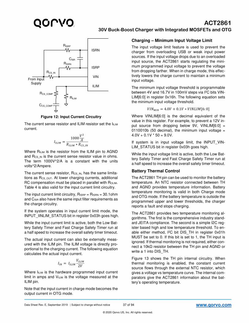
Data Sheet Rev. E, September 2019 | Subject to change without notice 37 of 94 www.qorvo.com
© 2020 Qorvo US, Inc. All rights reserved.
ACT2861
30V Buck-Boost Charger with Integrated MOSFETs and OTG
From Input Supply
RCS_IN
RILIM
RISRP
RISRN
CISR
ISRN
ISRP
VIN
ILIM
RCS_COMP
CCS_COMP
Figure 12: Input Current Circuitry
The current sense resistor and ILIM resistor set the IILIM
current.
= 1000
∗ _'
Where RILIM is the resistor from the ILIM pin to AGND
and RCS_IN is the current sense resistor value in ohms.
The term 1000V^2/A is a constant with the units
volts^2/Ampere.
The current sense resistor, RCS_IN, has the same limita-
tions as RCS_OUT. At lower charging currents, additional
RC compensation must be placed in parallel with ROLIM.
Table 4 is also valid for the input current limit circuitry.
The input current limit circuitry, RISRP = RISRN = 30.1ohm
and CISR also have the same input filter requirements as
the charge circuitry.
If the system operates in input current limit mode, the
INPUT_IINLIM_STATUS bit in register 0x03h goes high.
While the input current limit is active, both the Low Bat-
tery Safety Timer and Fast Charge Safety Timer run at
a half speed to increase the overall safety timer timeout.
The actual input current can also be externally meas-
ured with the ILIM pin. The ILIM voltage is directly pro-
portional to the charging current. The following equation
calculates the actual input current.
' =
2
Where IILIM is the hardware programmed input current
limit in amps and VILIM is the voltage measured at the
ILIM pin.
Note that the input current in charge mode becomes the
output current in OTG mode.
Charging – Minimum Input Voltage Limit
The input voltage limit feature is used to prevent the
charger from overloading USB or weak input power
sources. If the input voltage drops due to an overloaded
input source, the ACT2861 starts regulating the mini-
mum programmed input voltage to prevent the voltage
from dropping farther. When in charge mode, this effec-
tively lowers the charge current to maintain a minimum
input voltage.
The minimum input voltage threshold is programmable
between 4V and 16.7V in 100mV steps via I2C bits VIN-
LIM[6:0] in register 0x16h. The following equation sets
the minimum input voltage threshold.
(' = 4.0 + 0.1 ∗ ()*[6: 0] Where VINLIM[6:0] is the decimal equivalent of the
value in this register. For example, to prevent a 12V in-
put source from dropping below 9V, VINLIM[6:0] =
0110010b (50 decimal), the minimum input voltage =
4.0V + 0.1V * 50 = 9.0V.
If system is in input voltage limit, the INPUT_VIN-
LIM_STATUS bit in register 0x03h goes high.
While the input voltage limit is active, both the Low Bat-
tery Safety Timer and Fast Charge Safety Timer run at
a half speed to increase the overall safety timer timeout.
Battery Thermal Control
The ACT2861 TH pin can be used to monitor the battery
temperature. An NTC resistor connected between TH
and AGND provides temperature information. Battery
temperature monitoring is valid in both Charge mode
and OTG mode. If the battery temperature is outside the
programmed upper and lower thresholds, the charger
reports a fault and stops charging.
The ACT2861 provides two temperature monitoring al-
gorithms. The first is the comprehensive industry stand-
ard JEITA compliance. The second is a simple I2C reg-
ister based high and low temperature threshold. To en-
able either method, I2C bit DIS_TH in register 0x01h
MUST be set to 0. If this bit is set to 1, the TH input is
ignored. If thermal monitoring is not required, either con-
nect a 10kΩ resistor between the TH pin and AGND or
write a 1 into DIS_TH.
Figure 13 shows the TH pin internal circuitry. When
thermal monitoring is enabled, the constant current
source flows through the external NTC resistor, which
gives a voltage vs temperature curve. The internal com-
parators give the ACT2861 information about the bat-
tery’s operating temperature.
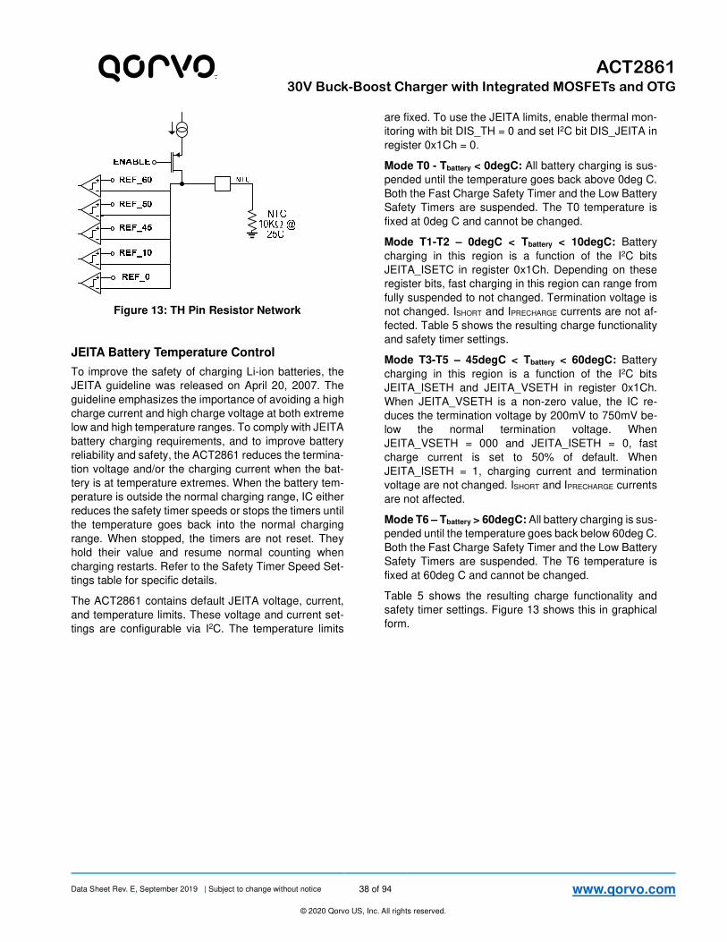
Data Sheet Rev. E, September 2019 | Subject to change without notice 38 of 94 www.qorvo.com
© 2020 Qorvo US, Inc. All rights reserved.
ACT2861
30V Buck-Boost Charger with Integrated MOSFETs and OTG
Figure 13: TH Pin Resistor Network
JEITA Battery Temperature Control
To improve the safety of charging Li-ion batteries, the
JEITA guideline was released on April 20, 2007. The
guideline emphasizes the importance of avoiding a high
charge current and high charge voltage at both extreme
low and high temperature ranges. To comply with JEITA
battery charging requirements, and to improve battery
reliability and safety, the ACT2861 reduces the termina-
tion voltage and/or the charging current when the bat-
tery is at temperature extremes. When the battery tem-
perature is outside the normal charging range, IC either
reduces the safety timer speeds or stops the timers until
the temperature goes back into the normal charging
range. When stopped, the timers are not reset. They
hold their value and resume normal counting when
charging restarts. Refer to the Safety Timer Speed Set-
tings table for specific details.
The ACT2861 contains default JEITA voltage, current,
and temperature limits. These voltage and current set-
tings are configurable via I2C. The temperature limits
are fixed. To use the JEITA limits, enable thermal mon-
itoring with bit DIS_TH = 0 and set I2C bit DIS_JEITA in
register 0x1Ch = 0.
Mode T0 - Tbattery < 0degC: All battery charging is sus-
pended until the temperature goes back above 0deg C.
Both the Fast Charge Safety Timer and the Low Battery
Safety Timers are suspended. The T0 temperature is
fixed at 0deg C and cannot be changed.
Mode T1-T2 – 0degC < Tbattery < 10degC: Battery
charging in this region is a function of the I2C bits
JEITA_ISETC in register 0x1Ch. Depending on these
register bits, fast charging in this region can range from
fully suspended to not changed. Termination voltage is
not changed. ISHORT and IPRECHARGE currents are not af-
fected. Table 5 shows the resulting charge functionality
and safety timer settings.
Mode T3-T5 – 45degC < Tbattery < 60degC: Battery
charging in this region is a function of the I2C bits
JEITA_ISETH and JEITA_VSETH in register 0x1Ch.
When JEITA_VSETH is a non-zero value, the IC re-
duces the termination voltage by 200mV to 750mV be-
low the normal termination voltage. When
JEITA_VSETH = 000 and JEITA_ISETH = 0, fast
charge current is set to 50% of default. When
JEITA_ISETH = 1, charging current and termination
voltage are not changed. ISHORT and IPRECHARGE currents
are not affected.
Mode T6 – Tbattery > 60degC: All battery charging is sus-
pended until the temperature goes back below 60deg C.
Both the Fast Charge Safety Timer and the Low Battery
Safety Timers are suspended. The T6 temperature is
fixed at 60deg C and cannot be changed.
Table 5 shows the resulting charge functionality and
safety timer settings. Figure 13 shows this in graphical
form.

Data Sheet Rev. E, September 2019 | Subject to change without notice 39 of 94 www.qorvo.com
© 2020 Qorvo US, Inc. All rights reserved.
ACT2861
30V Buck-Boost Charger with Integrated MOSFETs and OTG
Table 5: JEITA Mode Charging Safety Timer Configuration
Mode Temp JEITA_ISETC
[1:0] JEITA_ISETH JEITA_VSETH
Fast Charge
Current
Fast Charge
Safety Timer
PreCharge /
Short Current
Low
Battery
Safety
Timer
T0 <0C XX X XXX Suspended Stopped Suspended Stopped
T1 to T2
0C to
10C
00 X XXX Suspended Stopped Suspended Stopped
01 X XXX 25% of ICHG ½ Speed ISHRT / IPRECHG Full Speed
10 X XXX 50% of ICHG ½ Speed ISHRT / IPRECHG Full Speed
11 X XXX 100% of ICHG Full Speed ISHRT / IPRECHG Full Speed
T3 to T5 45C to
60C
XX X NOT 000 Reduced Voltage ½ Speed ISHRT / IPRECHG Full Speed
XX 1 000 Normal Full Speed ISHRT / IPRECHG Full Speed
XX 0 000 50% of ICHG ½ Speed ISHRT / IPRECHG Full Speed
T6 > 60C XX X XXX Suspended Stopped Suspend Stopped
Figure 13: JEITA Charging Profile
Non-JEITA Battery Temperature Control
The ACT2861 also includes non-JEITA battery temper-
ature control. Enable this mode by setting I2C bit
DIS_JEITA in register 0x1Ch = 1. In this mode, the IC
compares the battery voltage as measured on the TH
pin to two internal I2C registers: OTG_HOT[1:0] and
OTG_COLD, both in register 0x1D. If the temperature is
higher than OTG_HOT[1:0], all charging is suspended
and the safety timers are stopped. If the temperature is
lower than OTG_COLD, all charging is suspended and
the safety timers are stopped.
OTG_HOT[1:0] selects 55degC, 60degC, or 65degC.
Set this register = 11 to disable shutdown at hot temper-
atures. The OTG_COLD register selects between
0degC and -10degC. It is not possible to automatically
disable charging at low temperatures. However, a host
processor can read the battery temperature via the ADC
converter and manually disable charging.
Battery Path Impedance Compensation
The ACT2861 includes a Battery Path Impedance Com-
pensation feature that speeds the charging cycle. This
feature compensates for system level voltage drops due
to PCB, connector, wiring resistances, and battery pack
current sense resistances.
These voltage drops effectively reduce the voltage at
the battery. This results in the charger reaching the con-
stant voltage portion of the charge cycle too soon. Stay-
ing in constant current mode longer reduces the charg-
ing time.
The ACT286x allows the user to compensate for the
system level resistances by increasing the voltage reg-
ulation set point according to a formula that is propor-
tional to charging current and system resistance. This
feature is implemented with two I2C registers:
BAT_COMP_VCLAMP[2:0] and
BAT_PATH_COMP[2:0] in register 0x0Ch. The
BAT_COMP_VCLAMP[2:0] register sets the maximum
increase in charging voltage. This can be programmed
between 0mV and 420mV. The BAT_PATH_COMP[2:0]
register sets the system resistance between 0mΩ and
140mΩ.
For safe operation, if one register is set to a non-zero
value, the other register should also bet set to a non-
zero value. The maximum battery termination voltage is
set by the lower of the following two equations.
./#_#01 = 2#01_ + $% ∗ ./#_3/#$_3
./#_#01 = 2#01_ + ./#_3_2/3
Where VBAT_TERM is the new, compensated termination
voltage in volts, VVTERM_I2C is the I2C battery termination
voltage programmed in registers 0x12h and 0x11h, ICHG
is the actual charging current. RBAT_PATH_COMP is the pro-
grammed system impedance in ohms, and
VBAT_COMP_VCLAMP is the maximum allowable increase in
battery termination voltage.

Data Sheet Rev. E, September 2019 | Subject to change without notice 40 of 94 www.qorvo.com
© 2020 Qorvo US, Inc. All rights reserved.
ACT2861
30V Buck-Boost Charger with Integrated MOSFETs and OTG
Battery Full / Charging Termination
The ACT286x terminates a charge cycle when the bat-
tery reaches the termination voltage and the charge cur-
rent drops below the termination current. If the Input cur-
rent limit, Input Voltage limit, or Thermal Regulation loop
is active, the charger will not enter the Charge Full or
Charge Termination states.
Once the termination current and other requirements
are met, the charger transitions from the fast charge
state (FASTCHG) into either the charge full state
(CHGFULL) or charge termination state (CHGTERM).
When EN_TERM=0, the charger enters the CHGFULL
state. The Charge Full state functionality is the same as
the FASTCHG state. The charger can stay in the
CHGFULL state indefinitely. It keeps a fully charged
battery regulated to the VBAT_REG voltage. If some-
thing pulls current from the battery, the charger supplies
current to maintain the battery voltage at VBAT_REG.
The maximum charge current is still limited by the ex-
ternal OLIM resistor and the IFCHG[6:0] register.
When EN_TERM=1, the charger enters the CHGTERM
state. In this state, the charger is disabled and does not
supply any current to the battery. It monitors the battery
voltage to check for the condition when the battery volt-
age drops below VTERM-VRECHARGE. The
VRECHARGE voltage is typically 100mV or 150mV per
cell. Once the battery voltage drops below the threshold,
the IC enters the Fast Charge state and recharges the
battery.
See the state machine for more details charging and
charge termination.
Charging Safety Timers
The ACT2861 provides two internal charging safety tim-
ers: Low Battery Safety Timer and Fast Charge Safety
Timer
When the Battery Voltage is below VBAT_LOW and in the
charger is in the SCOND or PCOND states, a fixed 120
minute Low Battery Safety Timer is implemented. Dur-
ing this time, the Fast Charge Safety Timer is held in
reset and not active. If the Low Battery Safety timer
times out, the IC goes to the Charging Fault state until
it is reset – See below on how to clear the Low Battery
Safety Timer.
The Low Battery Safety Timer stops if the battery tem-
perature causes the converter to stop switching and en-
ter the SCSUSPEND or PCSUSPEND states. The Low
Battery Safety Timer runs at ½ speed if the Input Volt-
age, Input Current, or Die Temperature regulations
loops become active. This increases the overall time of
120 minute timer.
When the Battery Voltage is above VBAT_LOW the Fast
Charge Safety Timer is enabled and the Low Battery
Safety timer is held in reset. The Fast Charge Safety
Timer is controlled with the I2C bits
FC_SAFETY_TIMER[4:0] in register 0x1Bh. It is config-
urable between 30 minutes and 16 hours. If the Fast
Charge safety timer expires, the IC goes into the Charg-
ing Fault state and charging is disabled until the Fast
Charge Safety Timer is reset.
Both the Low Battery Safety and Fast Charge Safety
Timers can be fully disabled and reset via the I2C bit
DIS_SAFETY_TIMER in register 0x1Bh or manually
suspended using the I2C bit SUS-
PEND_SAFETY_TIMER in register 0x1Bh.
Both safety timers are automatically stopped any time
the charging is enabled but charging has suspended.
This occurs when the battery temperature exceeds the
allowable temperature limits.
Both safety timers also run at ½ speed when VIN Input
Regulation, IIN Current Regulation, or Die Thermal
Regulation are active to increase the overall safety timer
windows.
Additionally, the Fast Charge Safety Timer runs at ½
speed in some JEITA charging modes. See the JEITA
Battery Temperature Control paragraph for more details.
Both safety timers are reset when any of the following
occur:
1. Charging State Machine enters RESET state
2. DIS_SAFETY_TIMER register is set High
3. Charging has completed. This includes enter-
ing either the CHGFULL or CHG TERM states.
4. IC exits the Charge Mode via the EN_CHG pin,
OVERRIDE_EN_CHG, HIZ Registers, etc.
Data Sheet Rev. E, September 2019 | Subject to change without notice 41 of 94 www.qorvo.com
© 2020 Qorvo US, Inc. All rights reserved.
ACT2861
30V Buck-Boost Charger with Integrated MOSFETs and OTG
Table 6: Fast Charge Safety Timer Response
Condition Charge Response Fast Charge Safety Timer Speed
Normal Fast Charge NONE Full Speed
VIN Input Regulation Reduced Charge Current ½ Speed
IIN Input Current Regulation Reduced Charge Current ½ Speed
Thermal Die Regulation Reduced Charge Current ½ Speed
Battery Temp Exceed Limits Suspend Charge Suspend
Battery Temp Hot or Cold Reduced Charge Current or
VTERM
½ Speed
Table 7: Low Battery Safety Timer Response
Condition Charge Response Low Battery Safety Timer Speed
Normal SCOND or PCOND Charge NONE Full Speed
VIN Input Regulation Reduced Charge Current ½ Speed
IIN Input Current Regulation Reduced Charge Current ½ Speed
Thermal Die Regulation Reduced Charge Current ½ Speed
Battery Temp Exceeds JEITA T0 or T6 Limits Suspend Charge Suspend
Battery Temp Exceeds JEITA T1-T2 or T3-T5 Limits NONE Full Speed
Safety Timer Configuration Change
When the safety timer value needs to be changed, it is
recommended that the timer is first disabled. Then
change the FC_SAFETY_TIMER[4:0] register. Disable
the safety timer by writing a 1 into I2C bit
DIS_SAFETY_TIMER in register 0x1Bh. This proce-
dure ensures the safety timer properly restarts after new
value is configured.
Charger – Input Capacitor Selection
Note that the Charger CIN capacitors are also the OTG
output capacitors. They are connected to VIN. The input
capacitance should be a combination of ceramic and
bulk capacitance.
If the design only uses Charge mode and does not use
OTG mode, 22uF to 47uF capacitors are typically ac-
ceptable, but the final value is application dependent.
Choose the input capacitor value to keep the input volt-
age ripple less than ~50mV. The input capacitance can
be increased without limit.
C_4 = I$% ∗5678
59: ∗;<=567859: >
?@A∗BCDEEFG
Where CCHG_IN is the charging input capacitance (OTG
output capacitance) in uF, ICHG is the charging current in
Amperes, VBAT is the battery voltage in volts, VIN is the
input voltage in volts, FSW is the switching frequency in
Hz, and Vripple is the maximum input voltage ripple in
volts.
An additional 100uF bulk electrolytic capacitor is recom-
mended.
If the design uses OTG Mode, refer to the OTG Output
Capacitor Selection. The OTG Mode capacitor require-
ments take precedence over Charging input capaci-
tance.
Be sure to consider the input capacitor’s DC bias effects.
A capacitor’s actual capacitance is strongly affected by
its DC bias characteristics. The input capacitor is typi-
cally an X5R, X7R, or similar dielectric. Use of Y5U, Z5U,
or similar dielectrics is not recommended.
Input capacitor placement is critical for proper operation.
The input ceramic capacitor must be placed as close to
the IC as possible. The traces from VIN to the capacitor
and from the capacitor to PGND should as short and
wide as possible. Refer to the Layout Guidelines selec-
tion and to the EVK layout for details.

Data Sheet Rev. E, September 2019 | Subject to change without notice 42 of 94 www.qorvo.com
© 2020 Qorvo US, Inc. All rights reserved.
ACT2861
30V Buck-Boost Charger with Integrated MOSFETs and OTG
The bulk capacitor should be placed on the left side of
the current sense resistor.
Charger – Output Capacitor Selection
Note that the Charger COUT capacitor is also the OTG
input capacitor. It is connected directly to VBAT pin. The
capacitor should be dedicated high quality, low-ESR,
ceramic capacitor that is optimally placed to minimize
the power routing. 22uF to 47uF capacitors are typically
acceptable, but the final value is application dependent.
Choose the output capacitor value to keep the charger
output voltage ripple less than ~50-100mV. The output
capacitor can be increased without limit.
C_HI = I ∗5678
59: ∗;<=5JKL59: >
?@A∗BCDEEFG
Where CCHG_OUT is the charging output capacitance in
uF, ICHG is the charging current in Amperes, VBAT is the
battery voltage in volts, VIN is the input voltage in volts,
FSW is the switching frequency in Hz, and Vripple is the
maximum output voltage ripple in volts.
The ceramic capacitor PCB placement is critical. Refer
to the Layout Guidelines selection and to the EVK layout
for details.
Be sure to consider the input capacitor’s DC bias effects.
A capacitor’s actual capacitance is strongly affected by
its DC bias characteristics. The output capacitor is typi-
cally an X5R, X7R, or similar dielectric. Use of Y5U, Z5U,
or similar dielectrics is not recommended. Output ca-
pacitor placement is critical for proper operation. The
output capacitor must be placed as close to the IC as
possible. The traces from VBAT to the capacitor and
from the capacitor to PGND should as short and wide
as possible.
The bulk capacitor should be placed on the right side of
the current sense resistor.
OTG MODE
The ACT2861 supports on-the-go, OTG, mode buck-
boost converter operation. In this mode, the IC delivers
power from the battery to power other portable devices.
OTG Enable / Disable
The ACT2861 can only enter OTG mode from HIZ mode.
Note that if the IC is commanded to enter both OTG
mode and Charge mode at the same time, OTG mode
takes precedence. When in HIZ mode, OTG mode can
be enabled by the nOTG pin or I2C. In either case, the
I2C bit EN_OTG in register 0x0Eh must be = 1 to enable
OTG mode. Then pull the nOTG pin low to enter OTG
mode.
OTG Mode can also be enabled with the I2C bits
OTG_EN and OTG_EN_OVERRIDE in register 0x0Eh.
Setting OTG_EN = 1 enables OTG mode. Then set
OTG_EN_OVERRIDE = 1 to enter OTG mode. Note
that the OTG_EN_OVERRIDE bit overrides the nOTG
pin. Figure 14 shows both the hardware and I2C condi-
tions required to enter OTG mode.
Note that in all cases, the I2C bit HIZ in register 0x00h
must be = 0 to enter OTG mode. When HIZ = 1, the IC
is forced into HIZ mode and both OTG mode and
Charge mode are disabled.
HIZ bit = 0
OTG_EN bit = 1
nOTG pin = 0
OTG_EN_OVERRIDE bit = 1
HIZ to
OTG
Mode
Figure 14: Conditions to Enter OTG Mode from HIZ
Mode
After the IC is in OTG mode, the conditions to exit OTG
mode change. When OTG mode is disabled, the IC
state machine must go to HIZ mode or to SHIP mode.
There are several ways to disable OTG mode and go to
HIZ mode.
1. Set the I2C HIZ bit = 1
2. Set the I2C OTG_EN bit = 0
3. Pull the nOTG pin high and set the I2C
OTG_EN_OVERRIDE bit = 0.
4. The IC also exits OTG mode if there is an OTG
overvoltage condition for longer than 100ms.
OTG mode can also be disabled by putting the IC into
SHIP mode.
HIZ bit = 1
OTG_EN bit = 0
nOTG pin = 1
OTG_EN_OVERRIDE bit = 0
OTG to
HIZ
Mode
OTG_VOUT_OV bit = 1
100ms deglitch
Figure 15: Conditions to Enter HIZ Mode from OTG Mode
OTG Output Voltage Setting
The OTG output voltage is programmable between
2.96V and 23.42V in 20mV steps via by I2C bits
OTG_VOUT[9:0] in registers 0x13h and 0x14h.
#% = 2.96 + 20N ∗ OPQ_ORP[9: 0]

Data Sheet Rev. E, September 2019 | Subject to change without notice 43 of 94 www.qorvo.com
© 2020 Qorvo US, Inc. All rights reserved.
ACT2861
30V Buck-Boost Charger with Integrated MOSFETs and OTG
Where VOTG_VOUT[9:0] is the decimal equivalent of
the value in this register. For example, if
OTG_VOUT[9:0] = 0111000100b (452 decimal), the
output voltage = 2.96V + 0.02V * 452 = 12.00V.
When changing from one OTG output voltage to an-
other, the slew rate is programmable between 1V/ms
and 0.1V/ms by I2C bits OTG_OUTPUT_SLEW[1:0] in
register 0x10h. This allows the output to conform to
QC2.0/QC3.0/USB PD functions for higher output volt-
ages.
The battery voltage must always stay above the mini-
mum allowable battery voltage set by I2C bits
VBAT_LOW[6:0] in register 0x1Ah and
OTG_VBAT_CUTOFF[2:0] in register 0x0Fh. The ac-
tual voltage is the VBAT_LOW voltage minus the
OTG_VBAT_CUTOFF voltage. If the battery voltage
drops below this value, the IC turns off the OTG output
and goes to the OTG_RST state.
OTG Active Discharge
When changing the OTG output voltage to a higher level,
the switcher ramps the output voltage by the pro-
grammed slew rate. When the output voltage is pro-
grammed from a higher to a lower voltage, the voltage
drops at a rate determined by the output capacitance
and the load current. To minimize the fall time in no-load
conditions, the ACT2861 can provide a 70mA sink when
the output is transitioning to a lower output voltage. En-
able this feature by writing 1 into I2C bit OTG_PULL-
DOWN_RAMP. The 70mA load turns on until the output
voltage goes into regulation.
OTG Enable Delay
Once the OTG has the valid conditions for startup, the
OTG Enable Delay timer is enabled. The timer options
allow a 0ms to 1s delay. The OTG startup delay is con-
trolled by the I2C bits OTG_EN_DLY[1:0]
OTG Mode Soft Start
After the OTG Enable Delay has completed, the IC
starts the output using a soft start function programma-
ble by the I2C bits OTG_SS in register 0x0Eh. The
softstart time is independent of the output voltage set-
ting.
OTG Mode Constant Output Current
Regulation
After OTG mode soft start has completed, the IC moni-
tors the current on VIN input side sense resistor (ISRP
and ISRN) to provide constant current protection and
regulation in OTG mode. When the OTG output current
exceeds programmed value set by the ILIM pin and the
OTG_CC register, the switching converter changes to
output constant current mode and regulates a fixed out-
put current. In this case, the output voltage may drop if
the load resistance continues to decrease.
The maximum OTG output current is set by the same
resistor as the charger input current, Rcs_IN. Rcs_IN must
be set for the larger of the charge current or OTG cur-
rent. The maximum allowable OTG output current is 5A.
The actual output current limit, IOTG_OUT_LIM can be
scaled between 1% to 100% of IILIM in 1% steps. The
following equation defines the final OTG output current
limit.
#%_"#_ = ∗ OPQ_SS[6: 0] Where IILIM is the hardware programmed current limit
(see the Charging – Maximum Input Current section
for details) and OTG_CC[6:0] is the scaling factor.
OTG_CC[6:0] is the decimal equivalent value in this
register. For example, if IILIM, is programmed to 5A and
OTG_CC[6:0] = 0111100b (60% decimal), the final
charge current = 5A * 0.60 = 3A.
Note that OTG_CC[6:0] is a 7 bit register and can be
programmed between 0x00h and 0x7Fh (0% and
127%). If a value of 0x00h is written to the register, the
register retains 0x00h, but the IC sets the OTG scaling
factor to 1%. If a value above 0x64h (100%) is written
to the register, the IC retains the value, but sets the scal-
ing factor to 100%
The OTG regulation mode can be monitored in real time
by I2C bit OTG_Output_CC in register 0x20h. When this
bit = 0, the IC is regulating in output constant voltage
mode. When this bit = 1, the IC is regulating in constant
current mode. If the output drops below 3V, the IC as-
sumes an output fault has occurred and disables the
output for 3s. This is the OTG_HICCUP state. After 3s,
the state machine goes to OTG_RST and restarts. If a
short or high current fault is present after the restart, the
IC cycles back to OTG_HICCUP and OTG_RST. This
cycle continues indefinitely until OTG is disabled or the
fault is removed.
OTG Mode Constant Input Current Regulation
At all times during OTG mode, the IC monitors the cur-
rent on VBAT output side sense resistor (OSRP and
OSRN) to provide battery current protection.
The maximum OTG input current is set by the same re-
sistor as the charger output current, RCS_OUT. Unlike the
RCS_IN resistor, RCS_OUT does not have to be set to the
larger of the charge current or OTG input current. The
maximum allowable OTG input current is 5A. The max-
imum OTG input current limit, IOTG_IN_LIM, is a scaled ver-
sion of the programmed charge current, ICHG. IOTG_IN_LIM
is scaled to 150% or 200% of ICHG. This allows a larger
battery discharge current than charge current. The I2C

Data Sheet Rev. E, September 2019 | Subject to change without notice 44 of 94 www.qorvo.com
© 2020 Qorvo US, Inc. All rights reserved.
ACT2861
30V Buck-Boost Charger with Integrated MOSFETs and OTG
bits OTG_BAT_ILIM[1:0] in register 0x10h scale the
current. See the Setting Charge Current section for
details on programming ICHG.
Table 8: OTG I2C Input Current Limit Setting
OTG_BAT_ILIM[1:0]
Register Setting
OTG Input Current
00 OTG Disabled
01 150% of ICHG
10 200% of ICHG
11 300% of ICHG
When the OTG output current exceeds the maximum
programmed value, the switching converter changes to
input constant current mode and regulates a fixed input
current. The OTG regulation mode can be monitored in
real time by I2C bit OTG_BATTERY_CC in register
0x20h. When this bit = 0, the IC is not in OTG constant
current mode. When this bit = 1, the IC is regulating in
input constant current mode. If the output drops below
3V, the IC assumes an output fault has occurred and
disables the output for 3s. It follows the same flow as an
output current fault.
OTG Mode VIN Over-Voltage Protection
When in OTG mode, the IC provides power out of the
IC’s input. An input voltage should not be applied during
OTG Mode. To detect a possible plug in of a higher sup-
ply on VIN during OTG mode, the IC detects an over-
voltage condition on VIN (OTG output) and immediately
stops switching. The OTG overvoltage threshold is fixed
at 108% of the programmed OTG voltage. If the OV
condition lasts for more than 100ms, the IC exits OTG
Mode and enters HIZ Mode.
OTG – Cord Compensation
ACT286x provides cord compensation at the OTG out-
put. This feature compensates for system level voltage
drops due to PCB, connector, and wiring resistances.
These resistances reduce the output voltage at the load.
The ACT286x features Cord Compensation which al-
lows the user to compensate for these system level re-
sistances by increasing the OTG voltage regulation set
point proportional to the OTG output current. The output
voltage increases linearly with increasing load current.
The I2C OTG_CORD_COMP[1:0] bits in register 0x0F
set the Cord Comp value.
The Cord Compensation value is normalized to RCS_IN =
10mΩ and a 2.4A OTG load current. It scales linearly
with changes in current sense resistance or load current.
Note that the RCS_IN resistor is both the charging input
current limit resistor and the OTG output current limit
resistor.
TUV_TWX = #%_1Y_3 ∗ ZL[.\/ ∗ 1]^__`
a.a<Ω
Where VOTG_CORD_COMP is the I2C Cord Compensation
value of 100mV, 200mV, or 300mV per Table 9, IOTG is
the actual OTG output current in Amperes, and RCS_IN is
the current sense value in Ohms.
Table 9: OTG Cord Comp Setting
OTG_CORD_COMP[1:0]
Setting
Cord Comp
Value
Equivalent
System
Resistance
00 0 (Disabled) 0mΩ
01 100mV 41.7mΩ
10 200mV 83.3mΩ
11 300mV 125.0mΩ
Light Load Disable
The ACT2861 includes a Light Load Disable function in
OTG mode. This function disables OTG mode and puts
the IC into HIZ mode when the load drops very low. This
condition typically happens when the ACT2861 OTG
output is charging a portable device. When the portable
device is fully charged, the output current drops to 0A.
Light Load Disable minimizes battery current consump-
tion and extends battery life when the OTG output is not
needed.
Light Load Disable is available when the IC is operating
in OTG mode, the switcher is operating in buck mode,
VBAT is higher than VIN by a minimum of 0.5V, and the
OTG Output Voltage is less than 6V. Enable Light Load
Disable by setting I2C bit OTG_OFF_LOAD_EN in reg-
ister 0x0Eh = 1. Setting this bit = 0 disables the feature.
The minimum current is set to 5mA typical. The current
must be low for longer than the time set in I2C bit
OTG_OFF_DLY[1:0]. This time can programmed to 10s,
20s, or 30s.
Once the OTG state machine has detected a light load
condition, it enters the OTG_LL_DIS state. The IC must
exit OTG mode and re-enter OTG mode to restart the
converter. This is typically accomplished by toggling the
nOTG pin, but can also be accomplished via I2C.
OTG – Output Voltage DVS
The ACT2861 is ideally suited for many industry stand-
ard charging protocols such as USB PD3.0, QC2.0,

Data Sheet Rev. E, September 2019 | Subject to change without notice 45 of 94 www.qorvo.com
© 2020 Qorvo US, Inc. All rights reserved.
ACT2861
30V Buck-Boost Charger with Integrated MOSFETs and OTG
QC3.0, etc. This includes USB PD3.0 + PPD. To
achieve this compatibility, the output voltage can be dy-
namically changed in OTG mode. VOUT in OTG mode
can be dynamically changed by writing to the
OTG_VOUT[10:0] register, if internal feedback is used
and OTG_VOUT_I2C is set to 0. The OTG_OUT-
PUT_SLEW[1:0] register is used to control the slew rate
between settings when the OTG_VOUT[10:0] is
changed. When the voltage is increased, the internal
ramp and regulator can compensate and increase the
voltage. However, when the voltage is decreased, and
there is no external load on the output, the output volt-
age may not decrease fast enough to the meet the re-
quirements. To speed up the transition time from higher
to lower output voltages, set OTG_PULL-
DOWN_RAMP=1. This turns on an internal 70mA load
when the output voltage is stepped to a lower voltage
using the OTG_VOUT[10:0] register. The 70mA load
turns off when the voltage goes into regulation.
The ACT2861 also has a pulldown current that goes
active during any output overvoltage condition.
Enable this feature by setting the I2C bit OTG_PULL-
DOWN_OV = 1.
OTG Mode – State Machine Status
The I2C bits OTG_STATUS[2:0] in register 0x20h pro-
vide the user with real time status of the OTG state ma-
chine. These bits are always 000 when the IC is not in
OTG mode.
Table 10: OTG Cord Comp Setting
OTG_STATUS[2:0] State Machine State
000 OTG_RST
001 OTG_SS
010 OTG_REG
011 OTG_HICCUP
100 OTG_LL_DIS
101-111 Not Valid
OTG – Battery Temperature Protection
The ACT2861 provides battery temperature in OTG
mode. If the battery temperature goes outside the pro-
grammed range, the IC goes to the OTG_RST state. It
stays there until the temperature returns inside the pro-
grammed range or battery temperature monitoring is
disabled. Note that the OTG thermal limits use the same
registers as the non-JEITA charging registers.
Enable OTG battery temperature monitoring by setting
I2C bit DIS_TH = 0. When this feature is enabled, the IC
compares the battery voltage as measured on the TH
pin to two internal I2C registers: OTG_HOT[1:0] and
OTG_COLD, both in register 0x1Dh.
OTG - Frequency
The ACT2861 OTG switching frequency is the same as
the charging switching frequency. The ACT2861 can
operate at 125kHz, 250kHz, 500kHz, or 1MHz. The
switching frequency is set by the factory and is not user
programmable. The default frequency is 500kHz to give
the best tradeoff between size and efficiency, but can
be programmed to the other options with a custom CMI.
Note that the external component value requirements
change with different switching frequencies. Contact
[email protected] for additional information about
other configurations.
OTG – Input Capacitor Selection
Note that the OTG CIN capacitor is also the charging
output capacitor. It is connected directly to VBAT pin.
The capacitor should be dedicated high quality, low-
ESR, ceramic capacitor that is optimally placed to mini-
mize the power routing. 22uF to 47uF capacitors are
typically acceptable, but the final value is application de-
pendent. Choose the input capacitor value to keep the
OTG input voltage ripple less than ~50mV. The COTG in-
put capacitor can be increased without limit.
CI_4 = II ∗5c8d
59: ∗;<=5c8d59: >
?@A∗BCDEEFG Equation 6
Where COTG_IN is the OTG input capacitance (Charging
output capacitance) in uF, IOTG is the OTG output cur-
rent in Amperes, VOTG is the OTG output voltage in volts,
VIN is the OTG input voltage in volts, FSW is the switching
frequency in Hz, and Vripple is the maximum allowable
OTG input voltage ripple in volts.
If the OTG input source is a battery, no additional ca-
pacitance is needed. If the OTG input source is a power
supply rail, adding an additional 100 uF bulk electrolytic
capacitor is recommended.
The ceramic capacitor PCB placement is critical. Refer
to the Layout Guidelines selection and to the EVK layout
for details.
Be sure to consider the input capacitor’s DC bias effects.
A capacitor’s actual capacitance is strongly affected by
its DC bias characteristics. The input capacitor is typi-
cally an X5R, X7R, or similar dielectric. Use of Y5U, Z5U,

Data Sheet Rev. E, September 2019 | Subject to change without notice 46 of 94 www.qorvo.com
© 2020 Qorvo US, Inc. All rights reserved.
ACT2861
30V Buck-Boost Charger with Integrated MOSFETs and OTG
or similar dielectrics is not recommended. Input capaci-
tor placement is critical for proper operation. The input
capacitor must be placed as close to the IC as possible.
The traces from VBAT to the capacitor and from the ca-
pacitor to PGND should as short and wide as possible.
OTG – Output Capacitor Selection
Note that the OTG COUT capacitors are also the charg-
ing input capacitors. They are connected to VIN. The
output capacitance must be a combination of ceramic
and bulk capacitance.
Table 11 gives the required capacitor values for stability.
Note that the table has two output capacitor options:
Standard Capacitance and Minimum Capacitance.
The Standard Capacitance design requires more over-
all capacitance, but places no restriction on the bulk
capacitor ESR. The Minimum Capacitance design re-
sults in an overall smaller design, but places restrictions
on the ESR. The capacitor values can be increased
without limit.
Note that the Ceramic and Bulk capacitor values are
recommended “Capacitor Values”. When choosing the
ceramic capacitors, use X5R or X7R dielectrics and be
sure to consider the capacitor’s tolerance and DC bias
effects. Use of Y5U, Z5U, or similar dielectrics is not
recommended. The 22uF capacitor must have at least
9uF of effective capacitance for stability. The 47uF ca-
pacitor must have 19uF of capacitance. The bulk capac-
itors do not have DC bias effects.
Output ceramic capacitor placement is critical for proper
operation. The output capacitor must be placed as close
to the IC as possible. The traces from VIN to the capac-
itor and from the capacitor to PGND should as short and
wide as possible. The bulk capacitor should be placed
to the left of the current sense resistor. Refer to the Lay-
out Guidelines selection and to the EVK layout for
additional details.
OTG - Inductor Selection
The buck-boost regulator utilizes current-mode control
and a proprietary compensation scheme to simultane-
ously compensate the buck, buck-boost, and boost
modes of operation. The ACT2861 compensation re-
quires a fixed inductor value that is matched to the
switching frequency. Table 9 gives the required inductor
value. Choose an inductor with a low DC-resistance,
and avoid inductor saturation by choosing inductors with
DC ratings that exceed the maximum output current by
at least 30%. The inductor value must be within +30%
to -30% across all operating conditions.
OTG - Compensation
The ACT2861 operates in three switching modes: buck,
buck-boost, and boost mode depending on the input
and output voltage ratios. The IC contains a proprietary
compensation scheme to simultaneously compensate
all three switching modes. The compensation values
are directly tied to the switching frequency and required
inductor value. Table 9 provides the required compen-
sation values. Figure 16 shows the OTG compensation
components.
Table 11: OTG Inductor and Compensation
Standard Capacitance Design Minimum Capacitance Design
Switching
Frequency
Inductor
Min / Typ / Max
(uH)
CICOMP1
(nF)
CICOMP2
(nF)
RICOMP
(kΩ)
Ceramic
Capacitor
(uF)
Bulk
Capacitor
(uF)
Bulk
Capacitor
ESR
(mΩ)
Ceramic
Capacitor
(uF)
Bulk
Capacitor
(uF)
Bulk
Capacitor
ESR
(mΩ)
125Khz 29 / 42 / 55 82 8.2 20.0 47 1000 N/A 22 470 30 - 100
250Khz 15 / 22 / 29 39 3.9 20.0 47 470 N/A 22 220 50 - 200
500KHz 7 / 10 / 13 22 2.2 20.0 47 220 N/A 22 100 50 - 200
1MHZ 4 / 5.6 / 7.28 10 1.0 20.0 47 100 N/A 22 100 50 - 200

Data Sheet Rev. E, September 2019 | Subject to change without notice 47 of 94 www.qorvo.com
© 2020 Qorvo US, Inc. All rights reserved.
ACT2861
30V Buck-Boost Charger with Integrated MOSFETs and OTG
ICOMP
RICOMP1
CICOMP1
CICOMP2
Figure 16: OTG Compensation
CHARGE STATUS OUTPUT PIN (NCHG)
The ACT2861 indicates the Charging and OTG states
on the open drain nCHG pin. The nCHG pin typically
drives an LED, but can also be monitored by a micro-
processor GPIO. In Charge mode, the nCHG pin func-
tion is enabled by setting I2C bit DIS_nCHG_CHG in
register 0x00h = 0. Disable the function by setting it to
1. In OTG mode, the nCHG function is enabled by set-
ting the I2C bit EN_OTG_nCHG in register 0x0Fh = 1.
Disable the function by setting it to 0.
Tables 12 and 13 show the nCHG state in different
Charge and OTG operating conditions.
Table 12: nCHG Pin State in Charge Mode
Charging State nCHG Output Pin
Charging in progress LOW
Charging complete HIZ
Charge suspend or Fault Blinking at 1Hz
Table 13: nCHG Pin State in OTG Mode
OTG State nCHG Output Pin
OTG Enabled and Output Valid LOW
OTG Disabled HIZ
OTG Enabled In Fault, Hiccup, or
Light Load states HIZ
ADC Monitoring
General Description
The ACT2861 contains a built-in analog to digital con-
verter, ADC, which can be used to monitor seven sys-
tem level parameters. These include input voltage, out-
put voltage, input current, output current, TH pin, die
temperature, and the external ADC input pin. It uses a
single 12 bit delta-sigma ADC that uses an analog input
multiplexer to select one of seven channels for the A/D
conversion. The resulting digital results are stored in
seven digital registers. A seven to one multiplexer con-
nects one of the ADC output registers to the user ac-
cessible register map.
ADC Configuration
The ACT2861 ADC is configured through the I2C inter-
face. It is enabled and disabled by the I2C bit EN_ADC
in register 0x09h. The ADC has two conversion modes,
manual single-shot conversion and automatic polling
conversion.
Single-Shot Conversion
Configure the IC for single-shot conversion mode by
setting the following I2C bits in register 0x09h
ADC_ONE_SHOT = 1.
ADC_CH_SCAN = 0
DIS_ADCBUF = 0
In single shot mode, the user defines the input channel
to be converted and then manually initiates the ADC
conversion. I2C bits ADC_CH_CONV [2:0] in register
0x0Ah select the input channel to be converted.
ADC_CH_READ [2:0] selects the ADC channel to be
read. These should be set to the same channel. The
user initiates an ADC read by writing a 1 into EN_ADC
in register 0x09h. When ADC conversion is complete,
the ADC_DATA_READY bit in register 0x0Ah is set to
1, nIRQ is asserted low, and EN_ADC bit automatically
changes back to 0. The uP can then read the status bits
to find that the ADC conversion is complete. The ADC
data are stored in ADC_OUT [13:6] in register 0x07h
and ADC_OUT[5:2] in register 0x08h. nIRQ stays as-
serted low and the ADC_READY_BIT stays equal to 1
until the ADC data is read. Reading the ADC data auto-
matically deasserts nIRQ. To initiate another ADC con-
version for the same channel, set EN_ADC=1. To initi-
ate an ADC conversion for another channel, change
ADC_CH_CONV and ADC_CH_READ to the appropri-
ate channel and then set EN_ADC=1.
7 to 1MUX ADC
CH0
CH1
CH6
CH2
12 Bit Result
Clock
SEL[2:0]
Figure 17: ADC Block Diagram

Data Sheet Rev. E, September 2019 | Subject to change without notice 48 of 94 www.qorvo.com
© 2020 Qorvo US, Inc. All rights reserved.
ACT2861
30V Buck-Boost Charger with Integrated MOSFETs and OTG
Automatic Polling Conversion
Configure the IC for automatic polling conversion mode
by setting the following I2C bits in register 0x09h
ADC_ONE_SHOT = 0
ADC_CH_SCAN = 1
DIS_ADCBUF = 0
Start the automatic polling by changing EN_ADC to 1.
When in automatic polling mode, the ADC continuously
changes the MUX inputs to read all input channels. The
ADC continually overwrites the data in the output regis-
ter. After all channels have been converted, the
ADC_DATA_READY bit is set to 1. Note that nIRQ is
not asserted low in Automatic Polling mode. Ensure that
ADC data is valid and ready by reading the
ADC_DATA_READY before reading ADC data. After
the ADC_DATA_READY bit is set to 1, the user defines
the channel to be read with the ADC_CH_READ [2:0]
bits in register 0x0Ah. Change ADC_CH_READ to read
additional channels.
Table 14 shows the equations to convert the ADC data
into the actual measured values. Note that the table re-
fers to the voltages and currents with respect to Charge
mode.
Note that the klim term in the Output Current measure-
ment depends on IC’s operating mode and the
OTG_BAT_ILIM register setting (I2C register 0x10h).
Table 15 shows how to determine the correct klim value.
Table 14: ADC Channels
Channel Channel Description ADC_CH_CONV[2:0] ADC_CH_READ[2:0] Value
CH0 Input Current (IIN) 000 000 IIN = 0.7633*(ADC_OUT[13:2]-2048)
/RCS_IN/RlLIM
CH1 Input Voltage (VIN) 001 001 VIN = 0.02035*(ADC_OUT[13:2]-2048)
CH2 Output Voltage (VBAT) 010 010 VBAT = 0.01527*(ADC_OUT[13:2]-2048)
CH3 Output Current (IBAT) 011 011 IBAT = klim*0.7633*( ADC_OUT[13:2]-
2048)/RCS_OUT/ROLIM
CH4 TH 100 100 VTH = 0.003053*( ADC_OUT[13:2]-2048)
CH5 Die Temperature 101 101 TJ = 0.2707* ADC_OUT[13:2] - 809.49
CH6 ADC Input 110 110 VADC = 0.01527*(ADC_OUT[13:2]-2048)

Data Sheet Rev. E, September 2019 | Subject to change without notice 49 of 94 www.qorvo.com
© 2020 Qorvo US, Inc. All rights reserved.
ACT2861
30V Buck-Boost Charger with Integrated MOSFETs and OTG
Table 15: klim Values
IC Operating
Mode
OTG_BAT_ILIM
(register 0x10h) klim
Charge n/a 1
OTG
00 disabled
01 1.5
10 2.0
11 1.5
Below are two example ADC reads.
1. Charge mode. Battery voltage = 7.4V
Read CH2 to measure the battery voltage. This reading
results in the ADC_OUT[13:2] bits = 0x9E9h, which
converts to 2537 decimal.
./# = 0.01527 ∗ g2537 − 2048k = 7.04
2. OTG mode. OTG input current (from the battery) =
2.0A. Assume RCS_OUT = 0.01ohm and ROLIM =
33.1kohm. Also assume the OTG_BAT_ILIM register =
10
Read CH3 to measure the battery current. This reading
results in the ADC_OUT[13:2] = 0x9A4h, which con-
verts to 2468 decimal.
./# = lmnN ∗ 0.7633 ∗ g2468 − 2048k0.01 ∗ 33100 = 1.937

Data Sheet Rev. E, September 2019 | Subject to change without notice 50 of 94 www.qorvo.com
© 2020 Qorvo US, Inc. All rights reserved.
ACT2861
30V Buck-Boost Charger with Integrated MOSFETs and OTG
PC board layout guidance
Proper parts placement and PCB layout are critical to
the operation of switching power supplies. Follow the
following layout guidelines when designing the
ACT2861 PCB. Refer to the Active-Semi ACT2861
Evaluation Kit for layout guidance.
1. Place the ceramic input and output capacitors
as close as possible to the IC. Connect the in-
put capacitors directly between VIN and PGND
pins on the top layer. Connect the output capac-
itors directly between VBAT and PGND pins on
the top layer. Use 1206 sized capacitors to al-
low for proper switch pin routing. Note that the
input and output capacitor placement is critical.
Active-Semi strongly recommends following the
EVK input capacitor and output capacitor place-
ment and routing. The bulk input and output ca-
pacitor placement is not as critical. Bulk capac-
itors should be placed on the opposite side of
the sense resistors from the ceramic capacitors.
2. Minimize the switch node trace lengths be-
tween the SW1 and SW2 pins and the inductor.
Optimal switch node routing is to run the traces
between the input and output capacitors’ pads.
Using 1206 or larger sized capacitors is recom-
mended. Avoid routing sensitive analog signals
near these high frequency, high dV/dt traces.
Active-Semi strongly recommends following the
EVK inductor placement and PCB routing.
3. The VBATS pin should be Kelvin connected to
the battery. Keep this trace away from the SW1
and SW2 traces to prevent noise injection. The
IC regulates the battery voltage to this Kelvin
connection.
4. The PGND and AGND ground pins must be
electrically connected together. The AGND
ground plane should be isolated from the rest
of the PCB power ground. These two ground
pins should be connected together right at the
IC.
5. Connect the exposed pad directly to the top
layer PGND pins and ground plane. Connect
the top layer ground plane to both internal
ground planes and the PCB backside ground
plane with thermal vias. Provide ground plane
routing on multiple layers to allow the IC’s heat
to flow into the PCB and then spread radially
from the IC. Avoid cutting the ground planes or
adding vias that restrict the radial flow of heat.
6. Make Kelvin connections to the ILIM and OLIM
current sense resistors. Route the current
sense signals close to each other and keep
them away from noisy switching signals.
7. The current sense filter capacitors and induc-
tors should be placed directly by their respec-
tive ISRP, ISRN, OSRP, and OSRN pins.
8. Remember that all open drain outputs need
pull-up resistors.
9. The following components should be con-
nected to the AGND plane.
ILIM resistor
OLIM resistor
COMP resistor and capacitors
VREG bypass capacitor
INTBP bypass capacitor
10. The ACT2861 footprint must connect the VIN
pins 23, 24, and 35 on the top layer. It must con-
nect the SW1 pins 21, 22, and 34 on the top
layer. It must connect the SW2 pins 18, 19, and
33 on the top layer.
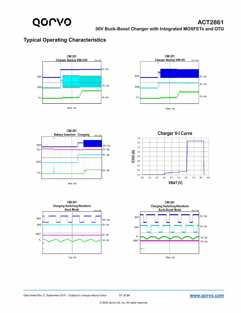
Data Sheet Rev. E, September 2019 | Subject to change without notice 51 of 94 www.qorvo.com
© 2020 Qorvo US, Inc. All rights reserved.
ACT2861
30V Buck-Boost Charger with Integrated MOSFETs and OTG
Typical Operating Characteristics

Data Sheet Rev. E, September 2019 | Subject to change without notice 52 of 94 www.qorvo.com
© 2020 Qorvo US, Inc. All rights reserved.
ACT2861
30V Buck-Boost Charger with Integrated MOSFETs and OTG

Data Sheet Rev. E, September 2019 | Subject to change without notice 53 of 94 www.qorvo.com
© 2020 Qorvo US, Inc. All rights reserved.
ACT2861
30V Buck-Boost Charger with Integrated MOSFETs and OTG

Data Sheet Rev. E, September 2019 | Subject to change without notice 54 of 94 www.qorvo.com
© 2020 Qorvo US, Inc. All rights reserved.
ACT2861
30V Buck-Boost Charger with Integrated MOSFETs and OTG

Data Sheet Rev. E, September 2019 | Subject to change without notice 55 of 94 www.qorvo.com
© 2020 Qorvo US, Inc. All rights reserved.
ACT2861
30V Buck-Boost Charger with Integrated MOSFETs and OTG

Data Sheet Rev. E, September 2019 | Subject to change without notice 56 of 94 www.qorvo.com
© 2020 Qorvo US, Inc. All rights reserved.
ACT2861
30V Buck-Boost Charger with Integrated MOSFETs and OTG

Data Sheet Rev. E, September 2019 | Subject to change without notice 57 of 94 www.qorvo.com
© 2020 Qorvo US, Inc. All rights reserved.
ACT2861
30V Buck-Boost Charger with Integrated MOSFETs and OTG
CMI OPTIONS
This section provides the basic default configuration settings for each available ACT2861 CMI option.
CMI 201: ACT2861QI201
CMI 201 is optimized for 2 cell Li-Ion battery applications and the default settings are appropriate for most typical appli-
cations. It operates with a switching frequency of 500kHz to provide an optimal tradeoff between overall size and effi-
ciency. Table 13 shows the default register settings.
Table 13: CMI 201 Default Register Settings
Function ACT2861QI201 Default
Register Settings Register
Battery & Charging
Battery Termination Voltage 8.4V VTERM
Battery Pre-Charge Voltage 6V VBAT_LOW
Battery Short Voltage 5V VBAT_SHORT
Battery Good Indicator Voltage (delta above Battery Pre-Charge Voltage)
0.6V VBATGOOD
Battery Recharge Voltage (delta below VTERM) 400mV VRECHARGE
Fast Charge Current Scaling Factor (relative to IOLIM) 50% IFCHG
Battery Short Current Scaling Factor (relative to IOLIM) 4% VBAT_SHORT_CURRENT
Battery Pre-Charge Current Scaling Factor (relative to IOLIM) 5% IPRECHG
Battery Termination Current Scaling Factor (relative to IOLIM) 5% ITERM
Battery Termination Enabled EN_TERM
Battery Charge Path Impedance Compensation Disabled BAT_PATH_COMP
Battery Path Impedance Compensation Voltage Clamp Disabled BAT_PATH_COMP_VCLAMP
Charging Input Current Limit Scaling Factor (relative to IILIM) 67% IINLIM
TH Pin Enabled DIS_TH
Non-JEITA Max Battery Temp 60 deg C OTG_HOT
Non-JEITA Min Battery Temp 0 deg C OTG_COLD
Minimum Input Voltage Limit (Start to reduce charger current)
4.5V VINLIM
Start Delay (charging) 220ms VIN_STRT_DLY
Battery OVP Latch off Disabled DIS_VBAT_OVP
Battery OV Deglitch Time 40ms VBAT_OV_DEGLITCH_EN
Safety Timer 16 Hr FC_SAFETY_TIMER
nCHG Pin Functionality in Charge Mode Enabled nOTG_PIN_POLARITY
JEITA
JEITA Support Enabled DIS_JEITA
JEITA Warm (45°C-60°C) Termination Voltage Reduction (below VTERM)
400mV JEITA_VSETH
JEITA Warm (45°C-60°C) Charge Current 50% JEITA_ISETH
JEITA Cold (0°C-10°C) Charge Current 50% JEITA_ISETC
OTG
OTG Operation Enabled OTG_EN

Data Sheet Rev. E, September 2019 | Subject to change without notice 58 of 94 www.qorvo.com
© 2020 Qorvo US, Inc. All rights reserved.
ACT2861
30V Buck-Boost Charger with Integrated MOSFETs and OTG
OTG Output Voltage 5.1V OTGVOUT_I2C
OTG Output Constant Current Limit Scaling Factor (relative to IILIM)
100% OTG_CC
OTG Mode Battery Discharge Current Limit Scaling Factor (relative to ICHG)
200% OTG_BAT_ILIM
OTG Softstart Time 5ms OTG_SS
Switching Frequency 500kHz FREQ_SEL
OTG nOTG Pin Polarity Active Low nOTG_PIN_POLARITY
nCHG Pin Functionality in OTG Mode Enabled EN_OTG_NCHG
OTG Start up Delay 1000ms OTG_EN_DLY
OTG Cord Compensation Disabled OTG_CORD_COMP
OTG Battery Cut Off Voltage During Discharge (Delta below VBAT_LOW)
0.4V OTG_VBAT_CUTOFF
OTG Output Slew Rate 0.5V/ms OTG_OUTPUT_SLEW
PFM Mode in Charge and OTG modes Enabled OTG_DIS_PFM
OTG Light Load Turn Off Enabled OTG_OFF_LOAD_EN
OTG Light Load Turn Off Delay 30s OTG_OFF_DLY
OCP Shutdown (8 FET OC cycles) Enabled DIS_OCP_SHUTDOWN
FET cycle by cycle current limit 10A FET_ILIMIT & ILIM_LOW
Input OV restart time 40ms VIN_OV_RESTART_DELAY
ADC
ADC Enabled Disabled EN_ADC
VREG LDO
VREG Enabled Enabled VREG_EN
VREG Output Voltage 5V VREG
VREG Input Control Auto VREG_OVERRIDE
VREG Input Voltage VIN VREG_SELECT
Miscellaneous
Watchdog Timer Disabled WATCHDOG
Die Regulation Temperature 120 deg C TREG
7-bit I2C Slave Address 0x24h I2CADD
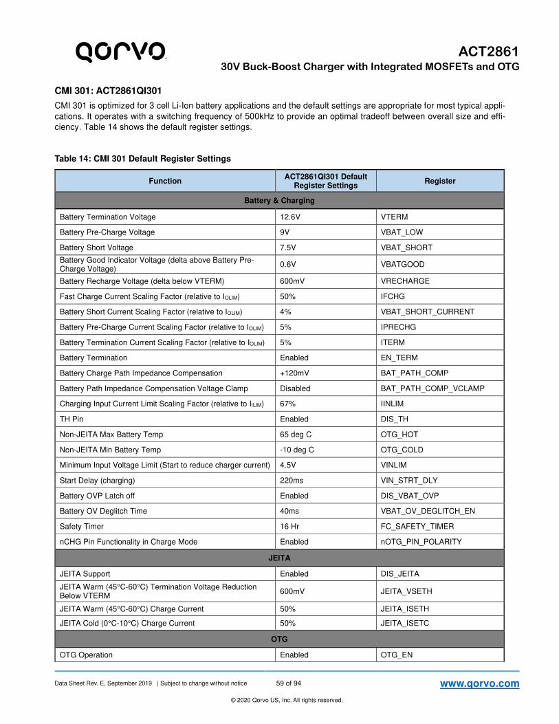
Data Sheet Rev. E, September 2019 | Subject to change without notice 59 of 94 www.qorvo.com
© 2020 Qorvo US, Inc. All rights reserved.
ACT2861
30V Buck-Boost Charger with Integrated MOSFETs and OTG
CMI 301: ACT2861QI301
CMI 301 is optimized for 3 cell Li-Ion battery applications and the default settings are appropriate for most typical appli-
cations. It operates with a switching frequency of 500kHz to provide an optimal tradeoff between overall size and effi-
ciency. Table 14 shows the default register settings.
Table 14: CMI 301 Default Register Settings
Function ACT2861QI301 Default
Register Settings Register
Battery & Charging
Battery Termination Voltage 12.6V VTERM
Battery Pre-Charge Voltage 9V VBAT_LOW
Battery Short Voltage 7.5V VBAT_SHORT
Battery Good Indicator Voltage (delta above Battery Pre-Charge Voltage)
0.6V VBATGOOD
Battery Recharge Voltage (delta below VTERM) 600mV VRECHARGE
Fast Charge Current Scaling Factor (relative to IOLIM) 50% IFCHG
Battery Short Current Scaling Factor (relative to IOLIM) 4% VBAT_SHORT_CURRENT
Battery Pre-Charge Current Scaling Factor (relative to IOLIM) 5% IPRECHG
Battery Termination Current Scaling Factor (relative to IOLIM) 5% ITERM
Battery Termination Enabled EN_TERM
Battery Charge Path Impedance Compensation +120mV BAT_PATH_COMP
Battery Path Impedance Compensation Voltage Clamp Disabled BAT_PATH_COMP_VCLAMP
Charging Input Current Limit Scaling Factor (relative to IILIM) 67% IINLIM
TH Pin Enabled DIS_TH
Non-JEITA Max Battery Temp 65 deg C OTG_HOT
Non-JEITA Min Battery Temp -10 deg C OTG_COLD
Minimum Input Voltage Limit (Start to reduce charger current) 4.5V VINLIM
Start Delay (charging) 220ms VIN_STRT_DLY
Battery OVP Latch off Enabled DIS_VBAT_OVP
Battery OV Deglitch Time 40ms VBAT_OV_DEGLITCH_EN
Safety Timer 16 Hr FC_SAFETY_TIMER
nCHG Pin Functionality in Charge Mode Enabled nOTG_PIN_POLARITY
JEITA
JEITA Support Enabled DIS_JEITA
JEITA Warm (45°C-60°C) Termination Voltage Reduction Below VTERM
600mV JEITA_VSETH
JEITA Warm (45°C-60°C) Charge Current 50% JEITA_ISETH
JEITA Cold (0°C-10°C) Charge Current 50% JEITA_ISETC
OTG
OTG Operation Enabled OTG_EN
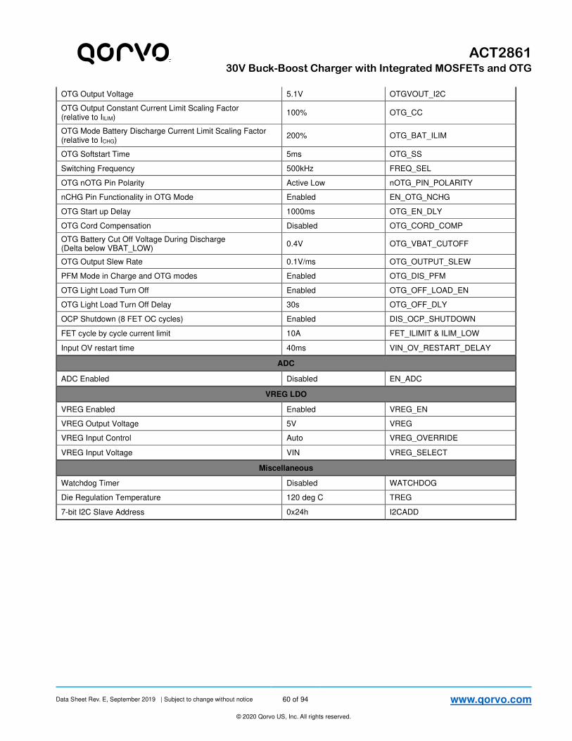
Data Sheet Rev. E, September 2019 | Subject to change without notice 60 of 94 www.qorvo.com
© 2020 Qorvo US, Inc. All rights reserved.
ACT2861
30V Buck-Boost Charger with Integrated MOSFETs and OTG
OTG Output Voltage 5.1V OTGVOUT_I2C
OTG Output Constant Current Limit Scaling Factor (relative to IILIM)
100% OTG_CC
OTG Mode Battery Discharge Current Limit Scaling Factor (relative to ICHG)
200% OTG_BAT_ILIM
OTG Softstart Time 5ms OTG_SS
Switching Frequency 500kHz FREQ_SEL
OTG nOTG Pin Polarity Active Low nOTG_PIN_POLARITY
nCHG Pin Functionality in OTG Mode Enabled EN_OTG_NCHG
OTG Start up Delay 1000ms OTG_EN_DLY
OTG Cord Compensation Disabled OTG_CORD_COMP
OTG Battery Cut Off Voltage During Discharge (Delta below VBAT_LOW)
0.4V OTG_VBAT_CUTOFF
OTG Output Slew Rate 0.1V/ms OTG_OUTPUT_SLEW
PFM Mode in Charge and OTG modes Enabled OTG_DIS_PFM
OTG Light Load Turn Off Enabled OTG_OFF_LOAD_EN
OTG Light Load Turn Off Delay 30s OTG_OFF_DLY
OCP Shutdown (8 FET OC cycles) Enabled DIS_OCP_SHUTDOWN
FET cycle by cycle current limit 10A FET_ILIMIT & ILIM_LOW
Input OV restart time 40ms VIN_OV_RESTART_DELAY
ADC
ADC Enabled Disabled EN_ADC
VREG LDO
VREG Enabled Enabled VREG_EN
VREG Output Voltage 5V VREG
VREG Input Control Auto VREG_OVERRIDE
VREG Input Voltage VIN VREG_SELECT
Miscellaneous
Watchdog Timer Disabled WATCHDOG
Die Regulation Temperature 120 deg C TREG
7-bit I2C Slave Address 0x24h I2CADD

Data Sheet Rev. E, September 2019 | Subject to change without notice 61 of 94 www.qorvo.com
© 2020 Qorvo US, Inc. All rights reserved.
ACT2861
30V Buck-Boost Charger with Integrated MOSFETs and OTG
CMI 401: ACT2861QI401
CMI 401 is optimized for 4 cell Li-Ion battery applications and the default settings are appropriate for most typical appli-
cations. It operates with a switching frequency of 500kHz to provide an optimal tradeoff between overall size and effi-
ciency. Table 15 shows the default register settings.
Table 15: CMI 401 Default Register Settings
Function ACT2861QI401 Default
Register Settings Register
Battery & Charging
Battery Termination Voltage 16.8V VTERM
Battery Pre-Charge Voltage 12V VBAT_LOW
Battery Short Voltage 10V VBAT_SHORT
Battery Good Indicator Voltage (delta above Battery Pre-Charge Voltage)
0.8V VBATGOOD
Battery Recharge Voltage (delta below VTERM) 800mV VRECHARGE
Fast Charge Current Scaling Factor (relative to IOLIM) 50% IFCHG
Battery Short Current Scaling Factor (relative to IOLIM) 4% VBAT_SHORT_CURRENT
Battery Pre-Charge Current Scaling Factor (relative to IOLIM) 5% IPRECHG
Battery Termination Current Scaling Factor (relative to IOLIM) 5% ITERM
Battery Termination Enabled EN_TERM
Battery Charge Path Impedance Compensation +120mV BAT_PATH_COMP
Battery Path Impedance Compensation Voltage Clamp Disabled BAT_PATH_COMP_VCLAMP
Charging Input Current Limit Scaling Factor (relative to IILIM) 67% IINLIM
TH Pin Enabled DIS_TH
Non-JEITA Max Battery Temp 65 deg C OTG_HOT
Non-JEITA Min Battery Temp -10 deg C OTG_COLD
Minimum Input Voltage Limit (Start to reduce charger current) 4.5V VINLIM
Start Delay (charging) 220ms VIN_STRT_DLY
Battery OVP Latch off Enabled DIS_VBAT_OVP
Battery OV Deglitch Time 40ms VBAT_OV_DEGLITCH_EN
Safety Timer 16 Hr FC_SAFETY_TIMER
nCHG Pin Functionality in Charge Mode Enabled nOTG_PIN_POLARITY
JEITA
JEITA Support Enabled DIS_JEITA
JEITA Warm (45°C-60°C) Termination Voltage Reduction Below VTERM
600mV JEITA_VSETH
JEITA Warm (45°C-60°C) Charge Current 50% JEITA_ISETH
JEITA Cold (0°C-10°C) Charge Current 50% JEITA_ISETC
OTG
OTG Operation Enabled OTG_EN
OTG Output Voltage 5.1V OTGVOUT_I2C

Data Sheet Rev. E, September 2019 | Subject to change without notice 62 of 94 www.qorvo.com
© 2020 Qorvo US, Inc. All rights reserved.
ACT2861
30V Buck-Boost Charger with Integrated MOSFETs and OTG
OTG Output Constant Current Limit Scaling Factor (relative to IILIM)
100% OTG_CC
OTG Mode Battery Discharge Current Limit Scaling Factor (relative to ICHG)
200% OTG_BAT_ILIM
OTG Softstart Time 5ms OTG_SS
Switching Frequency 500kHz FREQ_SEL
OTG nOTG Pin Polarity Active Low nOTG_PIN_POLARITY
nCHG Pin Functionality in OTG Mode Enabled EN_OTG_NCHG
OTG Start up Delay 1000ms OTG_EN_DLY
OTG Cord Compensation Disabled OTG_CORD_COMP
OTG Battery Cut Off Voltage During Discharge (Delta below VBAT_LOW)
0.4V OTG_VBAT_CUTOFF
OTG Output Slew Rate 0.1V/ms OTG_OUTPUT_SLEW
PFM Mode in Charge and OTG modes Enabled OTG_DIS_PFM
OTG Light Load Turn Off Enabled OTG_OFF_LOAD_EN
OTG Light Load Turn Off Delay 30s OTG_OFF_DLY
OCP Shutdown (8 FET OC cycles) Enabled DIS_OCP_SHUTDOWN
FET cycle by cycle current limit 10A FET_ILIMIT & ILIM_LOW
Input OV restart time 40ms VIN_OV_RESTART_DELAY
ADC
ADC Enabled Disabled EN_ADC
VREG LDO
VREG Enabled Enabled VREG_EN
VREG Output Voltage 5V VREG
VREG Input Control Auto VREG_OVERRIDE
VREG Input Voltage VIN VREG_SELECT
Miscellaneous
Watchdog Timer Disabled WATCHDOG
Die Regulation Temperature 120 deg C TREG
7-bit I2C Slave Address 0x24h I2CADD

Data Sheet Rev. E, September 2019 | Subject to change without notice 63 of 94 www.qorvo.com
© 2020 Qorvo US, Inc. All rights reserved.
ACT2861
30V Buck-Boost Charger with Integrated MOSFETs and OTG
I2C REGISTERS
The register map section provides a basic understanding of the ACT2861 registers. Note that the default values refer-
ence the CMI 201 settings.
Register Register Name Type R/W Description Default
0x00 Master Control 1 VM R/W
Configure various device options
0x00h
0x01 Master Control 2 NVM R/W 0x34h
0x02 General Status VM R Device status 0x00h
0x03 Charger Status VM R Charger status 0x00h
0x04 Temperature Status VM R Charger temperature status 0x00h
0x05 Fault 1 VM R Device Faults
0x00h
0x06 Fault 2 VM R 0x00h
0x07 ADC Output 1 VM R
ADC Output
0x00h
0x08 ADC Output 2 VM R 0x00h
0x09 ADC Configuration 1 VM R/W
ADC configuration bits
0x00h
0x0A ADC Configuration 2 VM R/W 0x00h
0x0B Charge Control VBAT
Short NVM R/W Configure various charger options 0x98h
0x0C Charge Control 2 NVM R/W Configure various charger options 0x40h
0x0D Charge Control 3 NVM R/W Configure various charger options 0x49h
0x0E OTG Mode Control 1 NVM R/W Configure OTG mode options 0xADh
0x0F OTG Mode Control 2 NVM R/W Configure OTG mode options 0x43h
0x10 OTG Control 3 NVM R/W Configure Converter options 0x78h
0x11 Battery Regulation
Voltage 1 NVM R/W
11-bit, 5V ~ 22.5V, LSB = 10mV, Default = 4.2V
0xF1h
0x12 Battery Regulation
Voltage 2 NVM R/W 0x54h
0x13 OTG Output Voltage 1 NVM R/W 10-bit, 3.0 ~ 23.42V, LSB = 20mV, Default = 5.1V
0xA0h
0x14 OTG Output Voltage 2 NVM R/W 0xD6h
0x15 Input Current Limit NVM R/W 7-bit, 0 ~ 100%, LSB = 1%, Default = 100% 0x43h
0x16 Input Voltage Limit NVM R/W 8-bit, 4 ~ 16.7V, LSB = 100mV, default = 4.4V 0x05h

Data Sheet Rev. E, September 2019 | Subject to change without notice 64 of 94 www.qorvo.com
© 2020 Qorvo US, Inc. All rights reserved.
ACT2861
30V Buck-Boost Charger with Integrated MOSFETs and OTG
0x17 OTG Output Current
Limit NVM R/W 7-bit, 0 ~ 100%, LSB = 1%, Default = 100% 0x64h
0x18 Fast Charge Current NVM R/W 7-bit, 0 ~ 100%, LSB = 1%, Default = 100% 0x32h
0x19 Pre-Charge &
Termination Current NVM R/W 4-bit, 0 ~ 20%, LSB = 1%, Default = 10% 0x00h
0x1A Battery Low Voltage NVM R/W 8-bit, 2.5 ~ 15.2V, LSB = 100mV, default = 3V 0x0Ah
0x1B Safety Timer NVM R/W 5-bit, 0.5 ~ 16V, LSB = 0.5Hr, default = 10Hr 0x1Fh
0x1C JEITA NVM R/W JEITA Charge Voltage/Current Setting 0x1Ah
0x1D Temperature Setting NVM R/W High/Low Temperature Thresholds 0x8Bh
0x1E IRQ Control 1 VM R/W
IRQ Mask Control
0x00h
0x1F IRQ Control 2 VM R/W 0x00h
0x20 OTG Status VM R OTG Status 0x00h

Data Sheet Rev. E, September 2019 | Subject to change without notice 65 of 94 www.qorvo.com
© 2020 Qorvo US, Inc. All rights reserved.
ACT2861
30V Buck-Boost Charger with Integrated MOSFETs and OTG
REG 0x00: Main Control 1 (R/W) (VM)
Bit Name
Defa
ult
Va
lue
Description Comment
7 HIZ 0 0: Not in HIZ mode
1: In HIZ mode
Bit to control if IC is in HIZ mode.
If set to 1, EN_CHG will NOT enable switching for
charger or and nOTG pin will not enable OTG mode. In
addition, the OVERRIDE_EN_CHG or the
OVERRIDE_nOTG Registers will not enable the
converter.
6 OVERRIDE_EN_CHG 0
0: No Effect
1: Override EN_CHG
Input
0: No effect
1: This will override the EN_CHG pin and allow the
charging to start, even if the EN pin is low. With this set
HI, enable pin will have no effect on charging. HIZ will
still need to be set to 0 to allow Charging.
5 SHIPM_ENTER 0
0: No Change
1: Device enters ship
mode
Write to 1 clears register after 1 sec
0: Normal Mode
1: Disables everything and device enters Ship Mode
after a 1 second delay. During the 1 second countdown
this bit will stay high. If user wants to cancel the enter
ship mode during the 1 sec delay, write this back to 0,
and ship mode will not be entered.
Warning: Entering ship mode disables everything and
must be re-enabled with SHIPM pin or VIN supply.
4 GPIO_OUT 0 0: Output in HIZ
1: Output pulled low
GPIO output register
Only available in ACT2862 (No OTG Mode)
3 DIS_nCHG_CHG 0 0: Enable
1: Disable
If set to 1, nCHG Charge pin is always HIZ in Charger
mode.
2 WATCHDOG_RESET
0
0: Normal
1: Reset
I2C Watchdog Timer Reset
This must be written to 1 before Watchdog timer expires,
if Watchdog timer is enabled. This is auto clearing when
writing to a 1.
1 Audio Frequency Limit 0 0: No limit
1: Minimum 31.25kHz
0: No limit of switching frequency
1: Set minimum switching frequency to 31.25kHz to
avoid audio noise
For both OTG and Charge mode.
0 REGISTER_RESET 0 1: Reset Registers to
Default
Register is self-clearing. Write to 1 resets registers and
set reset register back to 0.

Data Sheet Rev. E, September 2019 | Subject to change without notice 66 of 94 www.qorvo.com
© 2020 Qorvo US, Inc. All rights reserved.
ACT2861
30V Buck-Boost Charger with Integrated MOSFETs and OTG
REG 0x01: Main Control 2 (R/W) (NVM)
Bit Name
De
fau
lt V
alu
e
Description Comment
7 DIS_TH 0 0: Enable
1: Disable
Set 1 to disable TH output and the JEITA Control. During
this mode, charger and OTG mode will always operate at
full current and voltage settings.
Note: This must be set to 1 to achieve the lowest possible
input current.
6 DIS_OCP_SHUTDO
WN 0
0: Enable
1: Disable
If set to 0, the device will be disabled if FET cycle by cycle
current limit is detected for 8 (or 16) continuous cycles. For
both Charge and OTG modes. Uses the FET_LIMIT
register setting for the FET current limit.
5 DIS_VBAT_OVP 1 0: Enable
1: Disable
When set to 1, a BAT_OVP fault does not latch off the
charger in a fault mode. Charger will restart automatically
when the OVP condition is removed.
4 FET_ILIMIT 1 0: 8.5A
1: 10A
This is the cycle by cycle current limit setting for ALL FETS
in any operating mode:
3 VIN_OV_RESTART_
DELAY 0
0: 40ms
1: 100usec
Delay time to restart in charger mode after Input OV fault
has been removed
2 VREG_EN 1 0: Turn OFF VREG
1: Turn ON VREG
Control VREG on/off
Default is on.
1 WATCHDOG[1] 0 00: Disable timer
01: 80s
10: 160s
11: 320s
I2C Watchdog Timer Setting
Watchdog timer is always disabled and reset to 0 in HIZ
Mode.
When Disabled, Watchdog timer is also reset to 0. 0 WATCHDOG[0] 0

Data Sheet Rev. E, September 2019 | Subject to change without notice 67 of 94 www.qorvo.com
© 2020 Qorvo US, Inc. All rights reserved.
ACT2861
30V Buck-Boost Charger with Integrated MOSFETs and OTG
REG 0x02: General Status (Read Only) (VM)
Bit Name
De
fau
lt V
alu
e
Description Comment
7 nVBAT_GOOD 0
0: Battery voltage is good
1: Battery voltage is lower
than VBAT_GOOD
Set bit when battery voltage is lower than VBAT_GOOD
threshold in Charge Mode or OTG Mode
This is not checked in HIZ Mode, so will be set to 0 in HIZ
Mode.
This read only register has a 16msec deglitch for rising
and falling edge.
6 nIRQ_PIN_Status 0
0: Our device output drive
HIZ
1: Our device output
asserted Low
Device status of IRQ output
Not actual status of the IRQ pin – Open drain output so
other devices could be driving the pin low in a wired OR
configuration
5 nOTG_PIN_STATUS 0 0: nOTG Pin Low
1: nOTG Pin High
Real time status of the nOTG input pin
4 INPUT_UVLO_CHG 0 0: Input above UVLO
1: Input below UVLO
Charge Mode Only
Real time status – For latched fault, see the Fault
Registers
3 INPUT_OV_CHG 0 0: Input below OV
1: Input above OV
Charge Mode Only
Real time status – For latched fault, see the Fault
Registers
2 GPIO_IN 0 0: GPIO Input Low
1: GPIO Input HI
Real Time status of GPIO Pin.
Only available in ACT2862, otherwise this register is
always low
1 OPERATION_MODE[1] 0 00: HIZ Mode
01: Charger Mode
10: OTG Mode
11: not valid
Current state machine status for overall system
0 OPERATION_MODE[0] 0

Data Sheet Rev. E, September 2019 | Subject to change without notice 68 of 94 www.qorvo.com
© 2020 Qorvo US, Inc. All rights reserved.
ACT2861
30V Buck-Boost Charger with Integrated MOSFETs and OTG
REG 0x03: Charger Status (Read only) (VM)
Bit Name
De
fau
lt V
alu
e
Description Comment
7 EN_CHG_PIN_STAT
US 0
0: EN < 0.8V
1: EN > 0.8V
Real time status of the EN_CHG Input PIN
Threshold shown does not include hystersis
6 THERMAL_ACTIVE 0
0: Not in thermal regulation
1: Thermal regulation
Active
Thermal Regulation Active in Charge AND OTG Mode
5 INPUT_IINLIM_STAT
US 0
0: Not in IINLIM
1: In IINLIM
Charger Mode Only
4 INPUT_VINLIM_STAT
US 0
0: Not in VINLIM
1: In VINLIM
Charger Mode Only
3 CHG_STATUS[3] 0 0000: RESET
0001: SCOND or SCOND_DB
0010: SCSUSPEND
0011: PCOND
0100: PCSUSPEND
0101: FASTCHG
0110: FCSUSPEND
0111: CHGFULL
1000: CFSUSPEND
1001: CHGTERM
1010: CTSUSPEND
1011: FAULT
State machine for charger status
See Section 1.2.2. for further information
Notes:
When not in Charge State, status is always RESET (0000)
Check Register 0x06 Bit 0 to determine if Battery is below Dead Battery level.
1100 – 1111: Not Valid
2 CHG_STATUS[2] 0
1 CHG_STATUS[1] 0
0 CHG_STATUS[0] 0

Data Sheet Rev. E, September 2019 | Subject to change without notice 69 of 94 www.qorvo.com
© 2020 Qorvo US, Inc. All rights reserved.
ACT2861
30V Buck-Boost Charger with Integrated MOSFETs and OTG
REG 0x04: Temperature Status (Read Only) (VM)
Bit Name
De
fau
lt V
alu
e
Description Comment
7 POK_VOUT 0 0: Output below 90%
1: Output above 92%
Indicator for Power OK in OTG or CHG mode. Uses
OTG_VOUT setting and measures VIN Pin during OTG.
Uses VTERM setting and VBATS Pin during Charge
Mode.
6 TH_BAT_DETECT 0 0: No Battery detected
1: Battery detected
Uses the voltage on TH pin. Can be used to detect
battery or battery at very cold temperature. If DIS_TH=1,
then register is always 0 – No battery detected.
5 OTG_COLD_DIS /
CHRG DIS_JEITA=1 0
OTG Mode OR (Charge
Mode AND DIS_JEITA=1)
0: OK
1: Below 0°C / -10°C input
If this bit is 1, then OTG or Charger mode is disabled
caused by Battery Below 0C or -10C depending on
OTG_COLD Register
4 OTG_HOT_DIS /
CHRG DIS_JEITA=1 0
OTG Mode OR ( Charge
Mode AND
DIS_JEITA=1 )
0: OK
1: Above 55°C / 60°C /
65°C Threshold
If this bit is 1, then OTG or Charger mode is disabled
caused by Battery Above 55C/60C/65C depending on
OTG_HOT[1:0] Register
3 CHRG_COLD 0
0: Normal Charge Mode
OR DIS_JEITA=1
1: Charging has stopped
with DIS_JEITA=0
In charge mode, if DIS_JEITA=0, then this bit goes high
when the battery temperature is less than 0°C and the
device is always disabled.
2 CHRG_COOL 0
0: Normal Charge Mode
OR DIS_JEITA=1
1: Reduced current or
charge suspended
In charge mode, if DIS_JEITA=0, then this bit goes high
when battery temperature is between 10°C and 0°C. In
this mode, the device may be disabled, or reduced
current.
This is controlled by Register 0x1C Bit [1:0].
1 CHRG_WARM 0
0: Normal Charge Mode
OR DIS_JEITA=1
1: Reduced charge
voltage and/or current
In charge mode, if DIS_JEITA=0, then this bit goes high
when battery temperature is between 45°C and 60°C. In
this mode, the device may be have reduced current or
reduced VTERM. This is controlled by Register 0x1C Bit
[5:2].
0 CHRG_HOT 0
0: Normal Charge Mode
OR DIS_JEITA=1
1: Charging has stopped
In charge mode, if DIS_JEITA=0, then this bit goes high
when the battery temperature is greater than 60°C and
the device is always disabled.

Data Sheet Rev. E, September 2019 | Subject to change without notice 70 of 94 www.qorvo.com
© 2020 Qorvo US, Inc. All rights reserved.
ACT2861
30V Buck-Boost Charger with Integrated MOSFETs and OTG
REG 0x05: Faults 1 (Read only) (VM)
Bit Name
De
fau
lt V
alu
e
Description Comment
7 nIRQ_Clear 0 0: Normal Status
1: Clear IRQ output
Write this bit to 1 to clear the IRQ output. The bit will self-
clear to a 0 once the write occurs. If a fault still occurs, then
nIRQ pin may stay asserted low.
Register 0x02 Bit 6 provides a real time status of the nIRQ
output.
6 CHG_TIMER_EXPIR
ED 0
0: No Fault
1: Timer Expired
The VBAT LOW or Fast Charge Safety timer has expired –
Charge Only Mode.
Read to clear this latching fault bit.
Note: Reading this bit will not reset the fault timers. If the
fault timers are high, this bit will get set again immediately
after the read.
See the Safety Timer section on how to reset the Safety
Timers.
5 CHG_VBAT_OV 0 0: No Fault
1: VBAT OV
VBAT Overvoltage protection Charge Mode.
Read to clear this latching fault bit.
4 VREG_OC_UVLO 0 0: No Fault
1: VREG OC or UVLO
VREG_LDO Overcurrent or UVLO Charge Mode or OTG
Mode.
Read to clear this latching fault bit.
The fault mask bits DIS_CHG_VREG_FLT and
DIS_OTG_VREG_FLT registers do not affect this fault bit. It
will always get indicated here to notify the user.
Note: There is a 100msec restart delay for OC faults on the
VREG LDO, so the delay must expire before this bit can be
reset with a read to clear.
3 TSD 0 0: No Fault
1: Over Temperature
Die Thermal Shutdown in Charge mode or OTG Mode.
This bit is latching. Read this bit to clear the value back to 0.
This bit is not cleared if the fault is still present.
2 FET_OC 0 0: No Fault
1: Input OC
FET Overcurrent Shutdown in Charge mode or OTG Mode.
This bit is latching. Read this bit to clear the value back to 0.
This bit is not cleared if the fault is still present
1 CHG_MODE_INPUT
_OV 0
0: No Fault
1: Input Over Voltage
VIN OV in Charge Mode
Read to Clear latching Bit.
In Charge Mode, the OV fault time will be set by the delay
time in the VIN_OV_RESTART_DELAY Register. This 40ms
or 100usec delay must expire before a read to clear will
reset this register bit.
0 CHG_MODE_INPUT
_UV 0
0: No Fault
1: Charge VIN Under
Voltage
VIN UV in Charge Mode
Read to Clear latching Bit.

Data Sheet Rev. E, September 2019 | Subject to change without notice 71 of 94 www.qorvo.com
© 2020 Qorvo US, Inc. All rights reserved.
ACT2861
30V Buck-Boost Charger with Integrated MOSFETs and OTG
REG 0x06: Faults 2 (Read only) (VM)
Bit Name
Defa
ult
Va
lue
Description Comment
7 WATCHDOG_FA
ULT 0
0: No Fault
1: Watchdog Fault
Watchdog Timeout Fault
This bit is latching. If Watchdog is enabled and watchdog
timer times out, then this bit is set high.
This bit is not cleared when read. The watchdog timer is
cleared with a watchdog read or by disabling the watchdog
timer.
6 OTG_VOUT_FAU
LT 0
0: No Fault
1: OTG VOUT Fault
OTG Hiccup Mode Fault
This bit is latching. Read this bit to clear the value back to 0. If the VOUT enters hiccup state because current exceeds the Constant Current Mode, then this bit gets set.
This register will always be set during hiccup mode when
VOUT is off during the 3sec restart time and converter is in
the HICCUP state. After it exits this state, a read clears
this bit.
5 OTG_VBAT_CUT
OFF_FLT 0
0: No Fault
1: OTG VBAT CUTOFF Fault
OTG VBAT Cutoff Fault
This bit is latching. If VBAT falls below the VOTG_VBAT_CUTOFF
Voltage specified in the OTG_VBAT_CUTOFF Register
(Reg 0x0F, Bits 7:5), this bit is set to 1.
When the battery voltage is above the
OTG_VBAT_CUTOFF voltage, a read will clear this fault bit.
4 OTG_VOUT_OV 0
0: No Fault
1: VOUT OV Fault
OTG Vout Overvoltage Fault
Read to Clear latching bit
This bit will be set any time the Vout exceeds the OV
threshold for external or internal feedback. The VOUT
must be below the OV voltage and then a read will clear
this fault bit.
3 OTG_LIGHT_LO
AD 0
0: No Fault
1: OTG Off
Output Light Load State Latch
This bit is latching. This bit is set when the converter has
been disabled because of light load condition on output
and it entered the LL_DIS state. After the IC exits the
LL_DIS state, a read clears this bit.
2 OTG_VBAT_OV 0 0: No Fault
1: OTG VBAT OV
OTG VBAT Overvoltage fault
This bit is latching. This bit is set any time VBAT exceeds
the OV threshold in OTG mode. VBAT must be below the
OV voltage and then a read clears this bit.
1 I2C_FAULT 0 0: No Fault
1: I2C Fault
If set to 1, I2C command did not finish correctly or errors
on I2C data
0 DEADBATTERY 0 0: Battery above 3V
1: Battery below 3V
If charging and battery is below 3V, this bit gets set to 1.
This is a real-time indicator.

Data Sheet Rev. E, September 2019 | Subject to change without notice 72 of 94 www.qorvo.com
© 2020 Qorvo US, Inc. All rights reserved.
ACT2861
30V Buck-Boost Charger with Integrated MOSFETs and OTG
REG 0x07: ADC Output 1 (Read only) (VM)
Bit Name
De
fau
lt V
alu
e
Description Comment
7 ADC_OUT[13] 0
Selected data output from ADC_READ Register
ADC output
Upper 8 Bits of ADC output.
6 ADC_OUT[12] 0
5 ADC_OUT[11] 0
4 ADC_OUT[10] 0
3 ADC_OUT[9] 0
2 ADC_OUT[8] 0
1 ADC_OUT[7] 0
0 ADC_OUT[6] 0
REG 0x08: ADC Output 2 (Read only) (VM)
Bit Name
Defa
ult
Valu
e
Description Comment
7 RFU 0 Reserved for future use. Do not change this register value.
6 RFU 0
5 ADC_OUT[5] 0
Selected data output from ADC_READ Register
Lower 6 LSB Bits of ADC Output 4 ADC_OUT[4] 0
3 ADC_OUT[3] 0
2 ADC_OUT[2] 0
1 ADC_OUT[1] 0
0 ADC_OUT[0] 0

Data Sheet Rev. E, September 2019 | Subject to change without notice 73 of 94 www.qorvo.com
© 2020 Qorvo US, Inc. All rights reserved.
ACT2861
30V Buck-Boost Charger with Integrated MOSFETs and OTG
REG 0x09: ADC Configuration 1 (R/W) (VM)
Bit Name
De
fau
lt V
alu
e
Description Comment
7 EN_ADC 0 0: ADC disabled
1: ADC enabled
6 ADC_ONE_SHOT 0
0: ADC continually
converts data when
EN_ADC=1
1: ADC performs a one-
time conversion when
EN_ADC=1
[ADC ONE SHOT][ADC_ CH_SCAN] = XX operation is
described as below.
00 = Scan channel specified by ADC CHANNEL
CONVERSION [2:0] register bits repeatedly in a loop.
01 = Scan and convert channels 0 – 7 repeatedly in a loop.
10 = Convert channel specified by ADC CHANNEL
CONVERSION [2:0] once (one shot)
11 = Scan and convert channels 0 – 7 once and stop – one
loop 5 ADC_CH_SCAN 0
0: Scan single channel
specified by
ADC_CH_CONV
1: Scan all channels
4 DIS_ADC_BUFFER 0
0: ADC Buffer is
enabled
1: ADC Buffer is
disabled
This should always be set to 0.
3 ADC_SWAP 0
0: ADC Buffer is normal
inputs
1: ADC Buffer swaps
inputs
If very accurate measurements are required, the ADC input
pair can be swapped to negate input offset errors in the
Buffer AMP. This requires one read with ADC_SWAP=0
and one read with ADC_SWAP=1, then average the results.
2 HW_DIE_REV[2] 0
HW Die Revision
For use by Active Semi
1 HW_DIE_REV[1] 0
0 HW_DIE_REV[0] 0

Data Sheet Rev. E, September 2019 | Subject to change without notice 74 of 94 www.qorvo.com
© 2020 Qorvo US, Inc. All rights reserved.
ACT2861
30V Buck-Boost Charger with Integrated MOSFETs and OTG
REG 0x0A: ADC Configuration 2 (R/W) (VM)
Bit Name
De
fau
lt V
alu
e
Description Comment
7 ADC_DATA_READY 0 0: Data not ready
1: Data is ready
Read Only - Conversion occurred and data is ready to
read
6 RFU 0 Reserved for future use. Do not change this register
value.
5 ADC_CH_I2C_READ[2] 0 000 = ILIM Pin
001 = VIN
010 = VBAT
011 = OLIM
100 = TH
101 = Die temperature
110 = External Input
111 = AGND
This controls the current A2D register to output on the I2C
register. The A2D can provide an I2C read on a different
register while processing / converting another channel. 4 ADC_CH_I2C_READ[1] 0
3 ADC_CH_I2C_READ[0] 0
2 ADC_CH_CONV [2] 0 000 = ILIM Pin
001 = VIN
010 = VBAT
011 = OLIM
100 = TH
101 = Die temperature
110 = External Input
111 = AGND
This controls the current A2D conversion processing
channel. The A2D can provide an I2C read on a different
register while processing /converting another channel. 1 ADC_CH_CONV [1] 0
0 ADC_CH_CONV [0] 0

Data Sheet Rev. E, September 2019 | Subject to change without notice 75 of 94 www.qorvo.com
© 2020 Qorvo US, Inc. All rights reserved.
ACT2861
30V Buck-Boost Charger with Integrated MOSFETs and OTG
REG 0x0B: Charger Control 1 (R/W) (NVM)
Bit Name
De
fau
lt V
alu
e
Description Comment
7 VBAT_OV_DEGLITCH_EN 1
0: No Deglitch on OV
Fault
1: Deglitch of 40msec
In charge mode, deglitch for VBAT_OV to stop
charging and enter Fault Mode.
6 VBAT_SHORT[2] 0 000: 4V ( 2X2V )
001: 5V ( 2X2.5V )
010: 6V ( 3X2V)
011: 7.5V ( 3X2.5V)
100: 8V ( 4X2V )
101: 10V ( 4X2.5V )
110: 10V ( 5X2V )
111: 12.5V ( 5X2.5V)
Battery Short voltage threshold
Cross over from ISHRT to
IPRECHRG Current
5 VBAT_SHORT[1] 0
4 VBAT_SHORT[0] 1
3 VBAT_SHORT_CURRENT[1] 1 00: 1%
01: 2%
10: 4%
11: 8%
Battery charge current when VBAT less than VBAT
Short Voltage 2 VBAT_SHORT_CURRENT[0] 0
1 VREG_OVERRIDE 0 0: Automatic Control
1: Manual Control
0: The IC automatically selects the correct VREG input supply
1: Forces the IC to use the VREG input supply
defined by the VREG_SELECT register.
0 VREG_SELECT 0 0: VIN Supply
1: VBAT Supply
Defines the VREG input power source.

Data Sheet Rev. E, September 2019 | Subject to change without notice 76 of 94 www.qorvo.com
© 2020 Qorvo US, Inc. All rights reserved.
ACT2861
30V Buck-Boost Charger with Integrated MOSFETs and OTG
REG 0x0C: Charger Control 2 (R/W) (NVM)
Bit Name
De
fau
lt V
alu
e
Description Comment
7 ILIM_LOW 0 0: 8.5A or 10A 1: 5.7A
Lower ILIM setting for lower power applications. If set to 0, then uses FET_ILimit (Register 0x01 Bit 4) setting. If set to 1, then FET_ILimit should be set to 1 for 5.7A setting.
6 EN_TERM 1
0 Converter
continues to
operate:
1: Converter is
disabled when
termination is
reached
The bit determines what to do when charge current
drops below ITERM:
0: Converter stays on and continues to regulate
VBAT output to VTERM Voltage
5 BAT_PATH_COMP_VCLAMP[2] 0 000: Disable
001: VBAT + 60mV
010: VBAT + 120mV
011: VBAT + 180mV
100: VBAT + 240mV
101: VBAT + 300mV
110: VBAT + 360mV
111: VBAT + 420mV
Battery path impedance compensation voltage
clamp:
4 BAT_PATH_COMP_VCLAMP[1] 0
3 BAT_PATH_COMP_VCLAMP[0] 0
2 BAT_PATH_COMP [2] 0 000: Disable
001: 20mΩ
010: 40mΩ
011: 60mΩ
100: 80mΩ
101: 100mΩ
110: 120mΩ
111: 140mΩ
Battery Charging path impedance compensation
1 BAT_PATH_COMP[1] 0
0 BAT_PATH_COMP[0] 0

Data Sheet Rev. E, September 2019 | Subject to change without notice 77 of 94 www.qorvo.com
© 2020 Qorvo US, Inc. All rights reserved.
ACT2861
30V Buck-Boost Charger with Integrated MOSFETs and OTG
REG 0x0D: Charger Control 3 (R/W) (NVM)
Bit Name
De
fau
lt V
alu
e
Description Comment
7 VRECHARGE[2] 0
000: 200mV
001: 300mV
010: 400mV
011: 450mV
100: 500mV
101: 600mV
110: 750mV
111: 800mV
A battery voltage below VTERM restarts charging
when in the CHG Termination State.
Allows for 2-5 Cell with 100mV or 150mV setting or
200mV up to 4 cells.
6 VRECHARGE[1] 1
5 VRECHARGE[0] 0
4 VIN_STRT_DLY[1] 0 00: No delay
01: 220ms
10: 500ms
11: 1.3s
Delay time to start the charger when after the
charger is enabled
3 VIN_STRT_DLY[0] 1
2 DIS_CHG_VREG_FLT 0 0: Enable
1: Disable
If set to 0, an overcurrent or UVLO fault on the
VREG will stop charging mode (goes to FAULT
Mode). If set to 1, charging mode will continue with
fault on VREG.
1 VBATGOOD[1] 0 00: VBAT_LOW + 0.4V
01: VBAT_LOW + 0.6V
10: VBAT_LOW + 0.8V
11: VBAT_LOW + 1.0V
Battery good threshold reference to VBAT_LOW
Register setting for Charge Mode
0 VBATGOOD[0] 1
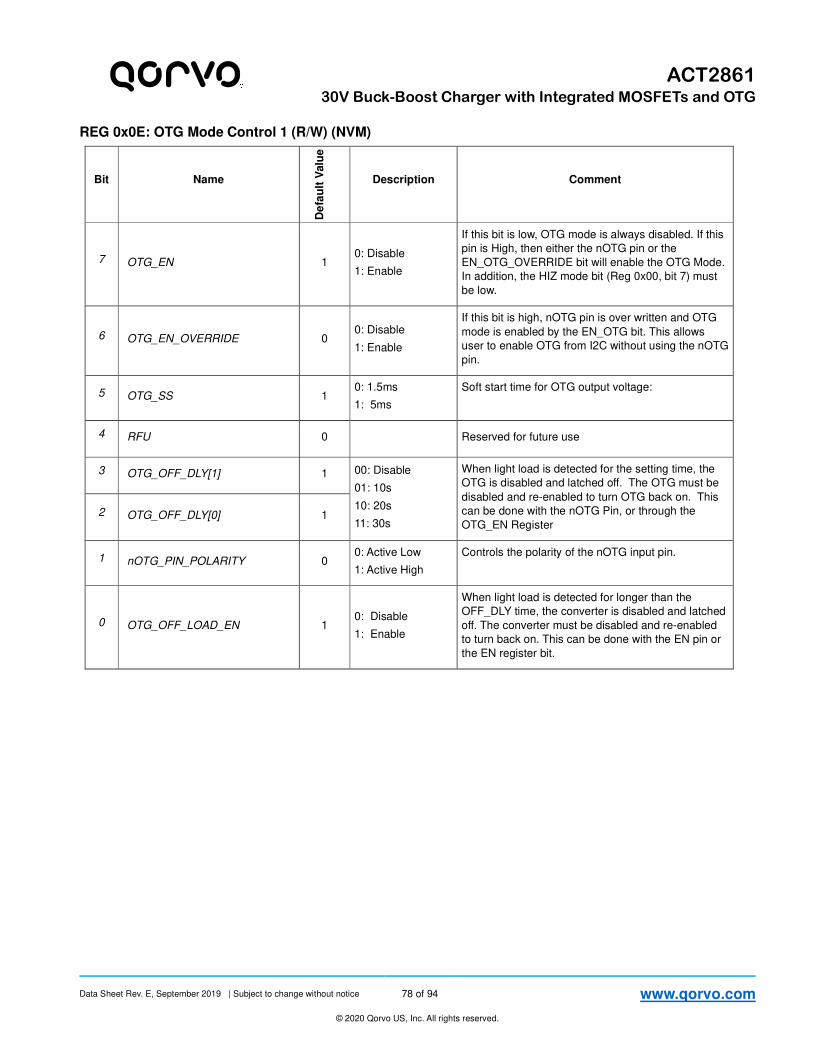
Data Sheet Rev. E, September 2019 | Subject to change without notice 78 of 94 www.qorvo.com
© 2020 Qorvo US, Inc. All rights reserved.
ACT2861
30V Buck-Boost Charger with Integrated MOSFETs and OTG
REG 0x0E: OTG Mode Control 1 (R/W) (NVM)
Bit Name
De
fau
lt V
alu
e
Description Comment
7 OTG_EN 1 0: Disable
1: Enable
If this bit is low, OTG mode is always disabled. If this
pin is High, then either the nOTG pin or the
EN_OTG_OVERRIDE bit will enable the OTG Mode.
In addition, the HIZ mode bit (Reg 0x00, bit 7) must
be low.
6 OTG_EN_OVERRIDE 0 0: Disable
1: Enable
If this bit is high, nOTG pin is over written and OTG
mode is enabled by the EN_OTG bit. This allows
user to enable OTG from I2C without using the nOTG
pin.
5 OTG_SS 1 0: 1.5ms
1: 5ms
Soft start time for OTG output voltage:
4 RFU 0 Reserved for future use
3 OTG_OFF_DLY[1] 1 00: Disable
01: 10s
10: 20s
11: 30s
When light load is detected for the setting time, the
OTG is disabled and latched off. The OTG must be
disabled and re-enabled to turn OTG back on. This
can be done with the nOTG Pin, or through the
OTG_EN Register 2 OTG_OFF_DLY[0] 1
1 nOTG_PIN_POLARITY 0 0: Active Low
1: Active High
Controls the polarity of the nOTG input pin.
0 OTG_OFF_LOAD_EN 1 0: Disable
1: Enable
When light load is detected for longer than the
OFF_DLY time, the converter is disabled and latched
off. The converter must be disabled and re-enabled
to turn back on. This can be done with the EN pin or
the EN register bit.

Data Sheet Rev. E, September 2019 | Subject to change without notice 79 of 94 www.qorvo.com
© 2020 Qorvo US, Inc. All rights reserved.
ACT2861
30V Buck-Boost Charger with Integrated MOSFETs and OTG
REG 0x0F: OTG Mode Control 2 (R/W) (NVM)
Bit Name
De
fau
lt V
alu
e
Description Comment
7 OTG_VBAT_CUTOFF[2] 0 000: VBAT_LOW
001: VBAT_LOW -0.2V
010: VBAT_LOW -0.4V
011: VBAT_LOW -0.6V
100: VBAT_LOW -0.8V
101: VBAT_LOW -1.0V
110: VBAT_LOW -1.2V
111: VBAT_LOW -1.4V
Battery Cut Off threshold for OTG mode to operate.
Referenced from VBAT_LOW level.
6 OTG_VBAT_CUTOFF[1] 1
5 OTG_VBAT_CUTOFF[0] 0
4 EN_OTG_nCHG 0 0: Disable
1: Enable
If EN_OTG_nCHG bit is 1, the IC pulls the nCHG pin
low in OTG mode to indicate the converter is running
in OTG.
If OTG is disabled for any reason, such as VIN Fault
or VBAT Cuttoff level, etc, nCHG goes high.
If set to 0, nCHG is always HIZ in OTG Mode.
3 OTG_CORD_COMP[1] 0 00: Disable
01: 100mV
10: 200mV
11: 300mV
OTG Cord Compensation at 2.4A Load with 10mΩ
resistor 2 OTG_CORD_COMP[0] 0
1 OTG_EN_DLY[1] 1 00: 0ms
01: 200ms
10: 500ms
11: 1s
The delay before enabling the OTG output from the
nOTG pin or OTG register bit.
0 OTG_EN_DLY[0] 1

Data Sheet Rev. E, September 2019 | Subject to change without notice 80 of 94 www.qorvo.com
© 2020 Qorvo US, Inc. All rights reserved.
ACT2861
30V Buck-Boost Charger with Integrated MOSFETs and OTG
REG 0x10: OTG Mode Control 3 (R/W) (NVM)
Bit Name
De
fau
lt V
alu
e
Description Comment
7 OTG_OUTPUT_SLEW[1] 0 00: 1V/ms
01: 0.5V/ms
10: 0.33V/ms
11: 0.1V/ms
If OTG Mode is set to internal Feedback and output
voltage is changed using the OTG_VOUT register for
QC2.0/3.0 or USB PD voltage ramp, this register
controls the rate at which the output voltage changes. 6 OTG_OUTPUT_SLEW[0] 1
5 OTG_PULLDOWN_RAMP 1 0: Disable
1: Enable
If OTG_PULLDOWN_RAMP is set to 1 and OTG_I2C
is set to 0 for internal Feedback, an internal current
source pulls down on the OTG output during a ramp
down of the output voltage. This allows the OTG
output to meet the QC 2.0/3.0 and USB PD ramp
timing requirements.
4 OTG_PULLDOWN_OV 1 0: Disable
1: Enable
If OTG_PULLDOWN_OV is set to 1, the pulldown
current source pulls down on the OTG output during
any OV condition on the output.
3 OTG_BAT_ILIM[1] 1 00: Disable
01: 150% of
IFCHG
10: 200% of
IFCHG
11: 150% of
IFCHG
The OTG input current limit scaling factor relative to
the hardware programmed OLIM current setting.
2 OTG_BAT_ILIM[0] 0
1 DIS_OTG_VREG_FLT 0 0: Enable
1: Disable
If set to 0, an Overcurrent or UVLO fault on the VREG
will stop OTG mode. If set to 1, OTG mode will
continue with fault on VREG.
0 OTG_DIS_PFM 0 0: Enable
1: Disable
Disable PFM mode in OTG or Charge mode to set a
fixed switching frequency.

Data Sheet Rev. E, September 2019 | Subject to change without notice 81 of 94 www.qorvo.com
© 2020 Qorvo US, Inc. All rights reserved.
ACT2861
30V Buck-Boost Charger with Integrated MOSFETs and OTG
REG 0x11: Battery Regulation Voltage 1 (R/W) (NVM)
Bit Name
De
fau
lt V
alu
e
Description Comment
7 VREG[4] 1 1600mV VREG LDO Output Voltage
Offset: 2V
Range: 2V (00000) - 5.1V (11111)
6 VREG[3] 1 800mV
5 VREG[2] 1 400mV
4 VREG[1] 1 200mV
3 VREG[0] 0 100mV
2 VTERM[10] 0 10240 mV Charge Voltage:
See Register 0x11 for details 1 VTERM[9] 0 5120 mV
0 VTERM[8] 1 2560 mV
REG 0x12: Battery Regulation Voltage 2 (R/W) (NVM)
Bit
Name
Defa
ult
Valu
e
Description Comment
7 VTERM[7] 0 1280 mV Charge Voltage
Offset: 5V
Range: 5V to 22.5V
5V: 000_0000_0000
22.5V: 110_1101_0110
Voltage over 22.5V will be set at 22.5V
Range: (110_1101_0111 to (111_1111_1111) = 22.5V
6 VTERM[6] 1 640 mV
5 VTERM[5] 0 320 mV
4 VTERM4] 1 160 mV
3 VTERM[3] 0 80 mV
2 VTERM[2] 1 40 mV
1 VTERM[1] 0 20 mV
0 VTERM[0] 0 10 mV

Data Sheet Rev. E, September 2019 | Subject to change without notice 82 of 94 www.qorvo.com
© 2020 Qorvo US, Inc. All rights reserved.
ACT2861
30V Buck-Boost Charger with Integrated MOSFETs and OTG
REG 0x13: OTG Output Voltage 1 (R/W) (NVM)
Bit Name
De
fau
lt V
alu
e
Description Comment
7 RFU 1
Reserved for future use. Do not change this register
value.
6 RFU 0
5 RFU 1
4 RFU 0
3 OTGVOUT_I2C 0
0: I2C Register
1: External
Resister Divider
using IFB
When set to 0, the OTG output voltage is controlled by
the OTG_VOUT registers.
When set to 1, the output voltage is controlled by an
external resistor divider connected to the IFB pin.
2 OTG_VOUT[9] 0 10240 mV Internal divider network
Offset: 2.96V
Range: 2.96V (000_0000_0000) to 23.42V
(111_1111_1111)
1 OTG_VOUT[8] 0 5120 mV
0 OTG_VOUT[7] 0 2560 mV

Data Sheet Rev. E, September 2019 | Subject to change without notice 83 of 94 www.qorvo.com
© 2020 Qorvo US, Inc. All rights reserved.
ACT2861
30V Buck-Boost Charger with Integrated MOSFETs and OTG
REG 0x14: OTG Output Voltage 2 (R/W) (NVM)
Bit Name
De
fau
lt V
alu
e
Description Comment
7 OTG_VOUT[6] 1 1280 mV Internal divider network
Offset: 2.96V
Range: 2.96V (000_0000_0000) to 23.42V
(111_1111_1111)
6 OTG_VOUT[5] 1 640 mV
5 OTG_VOUT[4] 0 320 mV
4 OTG_VOUT[3] 1 160 mV
3 OTG_VOUT[2] 0 80 mV
2 OTG_VOUT[1] 1 40 mV
1 OTG_VOUT[0] 1 20 mV
0 NA 0 No Function
REG 0x15: Input Current Limit (R/W) (NVM)
Bit Name
De
fau
lt V
alu
e
Description Comment
7 DIS_IIN_Limit 0 0: Enable
1: Disable
Disable input current limit
6 IINLIM[6] 1 64% The input current limit scaling factor relative to the
hardware programmed ILIM current setting.
Range: 1% (000_0001) to 100% (110_0100)
Setting 110_0100 to 111_1111 = 100%
Setting 000_0000 to 000_0001 = 1%
5 IINLIM[5] 0 32%
4 IINLIM[4] 0 16%
3 IINLIM[3] 0 8%
2 IINLIM[2] 0 4%
1 IINLIM[1] 1 2%
0 IINLIM[0] 1 1%

Data Sheet Rev. E, September 2019 | Subject to change without notice 84 of 94 www.qorvo.com
© 2020 Qorvo US, Inc. All rights reserved.
ACT2861
30V Buck-Boost Charger with Integrated MOSFETs and OTG
REG 0x16: Input Voltage Limit (R/W) (NVM)
Bit Name
De
fau
lt V
alu
e
Description Comment
7 DIS_VIN_Limit 0 0: Enable
1: Disable
Disable input voltage limit
6 VINLIM[6] 0 6400 mV Input voltage limit threshold.
Charge current will be reduced to regulate input
voltage at setpoint when in Charge Mode.
Offset: 4.0V
Range: 4.0V (000_0000) to 16.7V (111_1111)
5 VINLIM[5] 0 3200 mV
4 VINLIM[4] 0 1600 mV
3 VINLIM[3] 0 800 mV
2 VINLIM[2] 1 400 mV
1 VINLIM[1] 0 200 mV
0 VINLIM[0] 1 100 mV
REG 0x17: OTG Mode Output Current Limit (R/W) (NVM)
Bit Name
Defa
ult
Valu
e
Description Comment
7 OTG_DIS_CC 0 0: Enable
1: Disable
Set 1 to disable the output constant current limit
function in OTG Mode
6 OTG_CC[6] 1 64% The OTG output current limit scaling factor relative to
the hardware programmed ILIM current setting.
(VIN side measured at ISRN and ISRP)
Range: 1% (000_0001) to 100% (110_0100)
Setting 110_0100 to 111_1111 = 100%
Setting 000_0000 to 000_0001 = 1%
5 OTG_CC[5] 1 32%
4 OTG_CC[4] 0 16%
3 OTG_CC[3] 0 8%
2 OTG_CC[2] 1 4%
1 OTG_CC[1] 0 2%
0 OTG_CC[0] 0 1%

Data Sheet Rev. E, September 2019 | Subject to change without notice 85 of 94 www.qorvo.com
© 2020 Qorvo US, Inc. All rights reserved.
ACT2861
30V Buck-Boost Charger with Integrated MOSFETs and OTG
REG 0x18: Fast Charge Current (R/W) (NVM)
Bit Name
De
fau
lt V
alu
e
Description Comment
7 RFU 0 Reserved for future use
6 IFCHG[6] 0 64% The fast charge current scaling factor relative to the
hardware programmed IOLIM current setting.
Range: 1% (000_0001) to 100% (110_0100)
Setting 110_0100 to 111_1111 = 100%
Setting 000_0000 to 000_0001 = 1%
5 IFCHG[5] 1 32%
4 IFCHG[4] 1 16%
3 IFCHG[3] 0 8%
2 IFCHG[2] 0 4%
1 IFCHG[1] 1 2%
0 IFCHG[0] 0 1%
REG 0x19: Pre-Charge & Termination Current (R/W) (NVM)
Bit Name
De
fau
lt V
alu
e
Description Comment
7 IPRECHG[3] 0 8% The pre-charge current scaling factor relative to the
hardware programmed IOLIM current setting.
Range: 5% (0000) ~ 20% (1111)
Default: 10% (0101)
Offset: 5%
6 IPRECHG[2] 0 4%
5 IPRECHG[1] 0 2%
4 IPRECHG[0] 0 1%
3 ITERM[3] 0 8% The termination current scaling factor relative to the
hardware programmed IOLIM current setting.
Range: 5% (0000) ~ 20% (1111)
Default: 10% (0101)
Offset: 5%
2 ITERM[2] 0 4%
1 ITERM[1] 0 2%
0 ITERM[0] 0 1%

Data Sheet Rev. E, September 2019 | Subject to change without notice 86 of 94 www.qorvo.com
© 2020 Qorvo US, Inc. All rights reserved.
ACT2861
30V Buck-Boost Charger with Integrated MOSFETs and OTG
REG 0x1A: Battery Low Voltage (R/W) (NVM)
Bit Name
De
fau
lt V
alu
e
Description Comment
7 RFU 0 Reserved for future use. Do not change this register
value.
6 VBAT_LOW[6] 0 6400 mV Battery low voltage setting where pre-charge
transitions to fast charge when charging.
Offset: 5V
Range: 5V (0000000) ~ 15.2V (1111111)
5 VBAT_LOW[5] 0 3200 mV
4 VBAT_LOW[4] 0 1600 mV
3 VBAT_LOW[3] 1 800 mV
2 VBAT_LOW[2] 0 400 mV
1 VBAT_LOW[1] 1 200 mV
0 VBAT_LOW[0] 0 100 mV

Data Sheet Rev. E, September 2019 | Subject to change without notice 87 of 94 www.qorvo.com
© 2020 Qorvo US, Inc. All rights reserved.
ACT2861
30V Buck-Boost Charger with Integrated MOSFETs and OTG
REG 0x1B: Safety Timer (R/W) (NVM)
Bit Name
De
fau
lt V
alu
e
Description Comment
7 RFU 0 Reserved for future use. Do not change this register value.
6 DIS_SAFETY_TIMER 0 0: Enable
1: Disable
Disables both the Fast Charge and VBAT Low safety timers.
This also resets both safety timers. When this bit is set to 1, the
timers are held in reset (at 0). When this bit is written back to 0,
the timers start counting.
5 SUSPEND_SAFETY_TIMER 0 0: Counting
1: Suspend
If this is set to 1, both the Fast Charge and VBAT Low Safety
Timers stop counting and retain their current timer value. When
this bit is written back to 0, the counter resumes counting from
where it was suspended. If the counter is disabled during a
suspend condition using the DIS_SAFETY_TIMER bit, the
counter is reset to 0, even if suspended. It is then held at 0
until SUSPEND_SAFETY_TIMER is set to 0.
DIS_SAFTETY_TIMER reset has priority over
SUSPEND_SAFETY_TIMER.
4 FC_SAFETY_TIMER[4] 1 8 hours Timer setting for the Fast Charge State only. When this timer
expires, Fast charging stops and sets the Timer Expired bit.
Range: 0.5 (00000) ~ 16 hours (11111)
Default: 10 hours (10011)
Offset: 0.5 hour
3 FC_SAFETY_TIMER[3] 1 4 hours
2 FC_SAFETY_TIMER[2] 1 2 hours
1 FC_SAFETY_TIMER[1] 1 1 hours
0 FC_SAFETY_TIMER[0] 1 30 mins
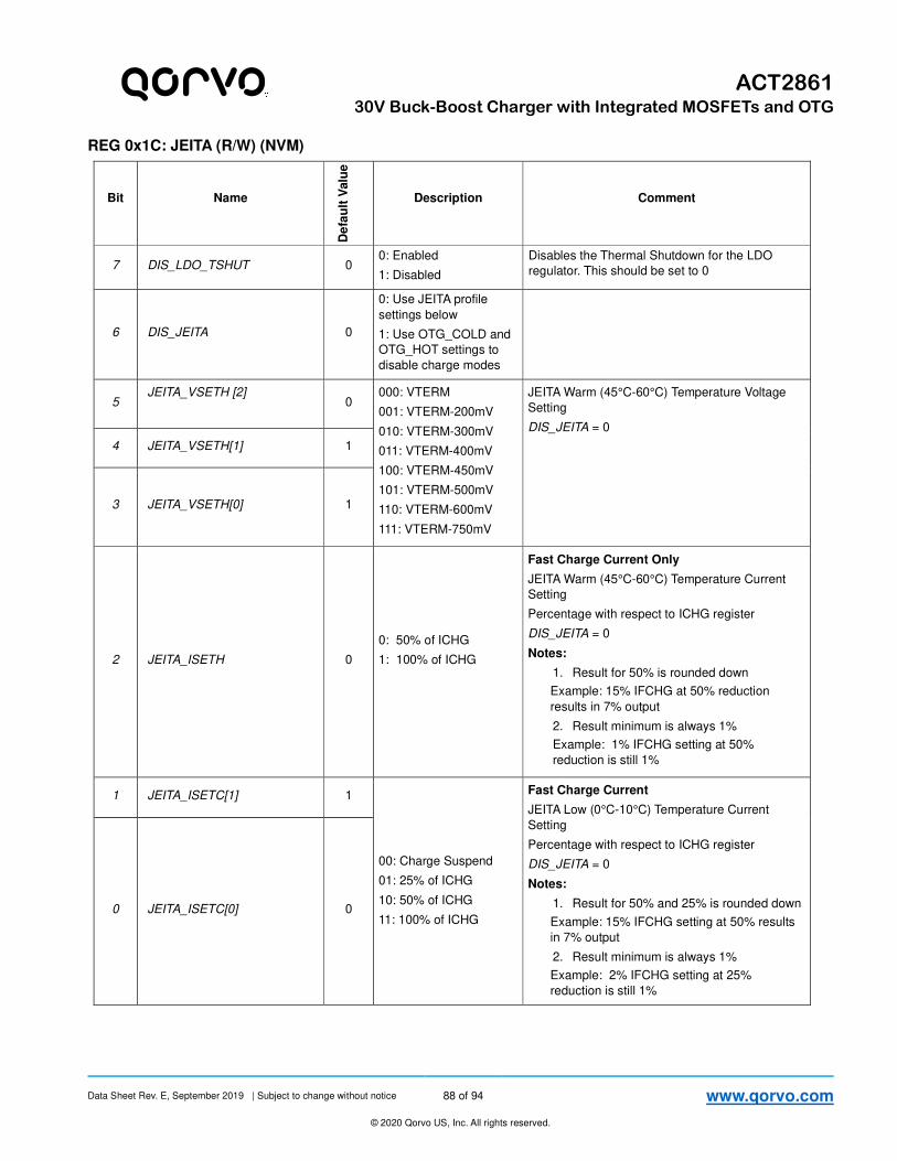
Data Sheet Rev. E, September 2019 | Subject to change without notice 88 of 94 www.qorvo.com
© 2020 Qorvo US, Inc. All rights reserved.
ACT2861
30V Buck-Boost Charger with Integrated MOSFETs and OTG
REG 0x1C: JEITA (R/W) (NVM)
Bit Name
De
fau
lt V
alu
e
Description Comment
7 DIS_LDO_TSHUT 0 0: Enabled
1: Disabled
Disables the Thermal Shutdown for the LDO
regulator. This should be set to 0
6 DIS_JEITA 0
0: Use JEITA profile
settings below
1: Use OTG_COLD and
OTG_HOT settings to
disable charge modes
5 JEITA_VSETH [2]
0
000: VTERM
001: VTERM-200mV
010: VTERM-300mV
011: VTERM-400mV
100: VTERM-450mV
101: VTERM-500mV
110: VTERM-600mV
111: VTERM-750mV
JEITA Warm (45°C-60°C) Temperature Voltage
Setting
DIS_JEITA = 0
4 JEITA_VSETH[1] 1
3 JEITA_VSETH[0] 1
2 JEITA_ISETH 0
0: 50% of ICHG
1: 100% of ICHG
Fast Charge Current Only
JEITA Warm (45°C-60°C) Temperature Current
Setting
Percentage with respect to ICHG register
DIS_JEITA = 0
Notes:
1. Result for 50% is rounded down
Example: 15% IFCHG at 50% reduction
results in 7% output
2. Result minimum is always 1%
Example: 1% IFCHG setting at 50%
reduction is still 1%
1 JEITA_ISETC[1] 1
00: Charge Suspend
01: 25% of ICHG
10: 50% of ICHG
11: 100% of ICHG
Fast Charge Current
JEITA Low (0°C-10°C) Temperature Current
Setting
Percentage with respect to ICHG register
DIS_JEITA = 0
Notes:
1. Result for 50% and 25% is rounded down
Example: 15% IFCHG setting at 50% results
in 7% output
2. Result minimum is always 1%
Example: 2% IFCHG setting at 25%
reduction is still 1%
0 JEITA_ISETC[0] 0

Data Sheet Rev. E, September 2019 | Subject to change without notice 89 of 94 www.qorvo.com
© 2020 Qorvo US, Inc. All rights reserved.
ACT2861
30V Buck-Boost Charger with Integrated MOSFETs and OTG
REG 0x1D: Temperature Setting (R/W) (NVM)
Bit Name
De
fau
lt V
alu
e
Description Comment
7 FREQ_SEL[1] 1
Frequency Selection
Settings for SMPS
00: 125kHz
01: 250kHz
10: 500kHz
11: 1MHz
Operation Frequency Settings
Note: These can NOT be changed “on the fly”
and each setting requires a different inductor
value and capacitors and compensation
components.
CARE SHOULD BE TAKEN WHEN WRITING
TO THIS REGISTER TO AVOID CHANGING
THE FREQUENCY WHILE OPERATING
6 FREQ_SEL[0] 0
5 DIS_SHIP_RENTER 0
0: Enable re-enter ship
mode
1: Disable ship mode re-
enter
If set to 0, writing to SHIPM_ENTER (Reg 0x00h
Bit 5) allows the IC to re-enter ship mode. If set to
1, the IC ignores the SHIPM_ENTER command.
4 OTG_HOT[1] 0 00: VTH55C at 55°C
01: VTH60C at 60°C
10: VTH65C at 65°C
11: Disable shutdown
OTG mode or Disable JEITA Mode Hot
Temperature Monitor TH / NTC Thresholds
3 OTG_HOT[0] 1
2 OTG_COLD 0 0: VTH0C at 0°C
1: VTH-10C at -10°C
OTG mode or Disable JEITA Mode Cold
Temperature Monitor TH / NTC Thresholds
1 TREG[1] 1 00: Disable
01: 80°C
10: 100°C
11: 120°C
Die temperature regulation threshold
0 TREG[0] 1

Data Sheet Rev. E, September 2019 | Subject to change without notice 90 of 94 www.qorvo.com
© 2020 Qorvo US, Inc. All rights reserved.
ACT2861
30V Buck-Boost Charger with Integrated MOSFETs and OTG
REG 0x1E: IRQ Control 1 R/W (VM)
Bit Name
De
fau
lt V
alu
e
Description Comment
7 nIRQ_CHGDONE 0 0: Either CHG Done state
triggers nIRQ pin
1: Masks nIRQ
If set to 0, any time the device enters the
CHGTERM or CHGFULL state, it activates the
nIRQ Pin
Setting to 1, masks CHG done states to nIRQ
6 nIRQ_VBAT_GOOD 0 0: VBAT_GOOD falling
edge triggers nIRQ
1: Masks nIRQ
If set to 0, VBAT_GOOD falling below threshold
actives the nIRQ Pin
Setting to 1, masks VBAT_GOOD to nIRQ
5 nIRQ_CHG_OVUV 0 0: Charge Mode OVUV
nIRQ
1: Masks nIRQ
If set to 0, a Overvoltage or Undervoltage on VIN
during charge mode activates the nIRQ Pin
Setting to 1, masks the Overvoltage or
Undervoltage to nIRQ
4 nIRQ_OTG_VBAT 0
0: OTG Mode VBAT
Cutoff or Over Votlage on
nIRQ
1: Masks nIRQ
If set to 0, a VBAT below VBAT Cuttoff or VBAT
Overvoltage during OTG mode activates the
nIRQ Pin
Setting to 1, masks the fault to nIRQ
3 nIRQ_SafetyTimer 0 0: Charge Mode safety
timer expired on nIRQ
1: Masks nIRQ
If set to 0, a VBAT Low safety timer expired or a
Fast Charge safety timer expired during charge
mode activates the nIRQ Pin
Setting to 1, masks the fault to nIRQ
2 nIRQ_CHG_VBAT_OV 0 0: Charge Mode VBAT
Overvoltage on nIRQ
1: Masks nIRQ
If set to 0, a VBAT Overvoltage during charge
mode activates the nIRQ Pin
Setting to 1, masks the fault to nIRQ
1 nIRQ_VREG_FLT 0
0: VREG LDO
Overcurrent or
Undervoltage indicated on
nIRQ
1: Masks nIRQ
If set to 0, a VREG LDO Overcurrent or
Undervoltage activates the nIRQ pin
Setting to 1, masks the fault to nIRQ
0 nIRQ_TSD 0
0: Device Thermal
Shutdown indicated on
nIRQ
1: Masks nIRQ
If set to 0, a device Thermal Shutdown activates
the nIRQ pin
Setting to 1, masks the fault to nIRQ

Data Sheet Rev. E, September 2019 | Subject to change without notice 91 of 94 www.qorvo.com
© 2020 Qorvo US, Inc. All rights reserved.
ACT2861
30V Buck-Boost Charger with Integrated MOSFETs and OTG
REG 0x1F: IRQ Control 2 R/W (VM)
Bit Name
De
fau
lt V
alu
e
Description Comment
7 nIRQ_FET_OC 0 0: FET Overcurrent
triggers nIRQ pin
1: Masks nIRQ
If set to 0, a FET Overcurrent condition activates
the nIRQ pin
Setting to 1, masks CHG done states to nIRQ
6 nIRQ_Watchdog 0 0: Watchdog timer
expired triggers nIRQ
1: Masks nIRQ
If set to 0, a watchdog timeout activates the
nIRQ pin
Setting to 1, masks the fault nIRQ
5 nIRQ_OTG_HICCUP 0 0: OTG Mode enter
Hiccup state nIRQ
1: Masks nIRQ
If set to 0, OTG Mode entering Hiccup state
activates the nIRQ pin
Setting to 1, masks hiccup mode to nIRQ
4 nIRQ_OTG_LL 0 0: OTG Mode enter Light
Load state on nIRQ
1: Masks nIRQ
If set to 0, OTG Mode entering Light Load
Disable state activates the nIRQ pin
Setting to 1, masks light load disable state to
nIRQ
3 nIRQ_A2D_DATA 0 0: A2D Data Ready
1: Masks A2D Data
Ready nIRQ
If set to 0, a rising edge on A2D Data Ready
activates the nIRQ pin
Setting to 1, masks the A2D Data Ready to nIRQ
2 nIRQ_HIZ 0 0: Enter HIZ Mode
1: Masks Enter HIZ Mode
nIRQ
If set to 0, a rising edge when entering HIZ State
activates the nIRQ pin
Setting to 1, masks the HIZ Enter to nIRQ
1 nIRQ_CHG_SUSPEND 0
0: Enter charge suspend
mode
1: Masks Enter charge
suspend mode nIRQ
If set to 0, a rising edge when entering a
suspend state in charge mode activates the
nIRQ pin
Setting to 1, masks the charge suspend enter to
nIRQ
0 nIRQ_OTG_BATTEMP 0 0: OTG BAT Temp Fault
1: Masks OTG BAT Temp
Fault nIRQ
If set to 0, a rising edge caused by Battery Temp
HOT or COLD in OTG Mode activates the nIRQ
pin
Setting to 1, masks the nIRQ

Data Sheet Rev. E, September 2019 | Subject to change without notice 92 of 94 www.qorvo.com
© 2020 Qorvo US, Inc. All rights reserved.
ACT2861
30V Buck-Boost Charger with Integrated MOSFETs and OTG
REG 0x20: IRQ / OTG Status (R/W) (VM)
Bit Name
De
fau
lt V
alu
e
Description Comment
7 nIRQ_I2C_ERROR 0
0: I2C Fault
1: Masks I2C Fault
nIRQ
If set to 0, a fault on the I2C command / I2C bus
activates the nIRQ Pin
Setting to 1, masks the nIRQ
6 OTG_BATTERY_CC 0
0: OTG Input from
battery no in current
limit
1: OTG input from
battery is regulating in
Constant Current Mode
OTG Mode Only
Real Time status
This is the current measured on the VBAT side using
OSRP and OSRN during OTG Mode controlled by
the OTG_BAT_ILIM Register
5 OTG_OUTPUT_CC 0
0: OTG Output
regulating using voltage
loop
1: OTG output is
regulating in Constant
Current Mode
OTG Mode Only
Real Time status
This is the current measured on the VIN side using
ISRP and ISRN during OTG Mode controlled by the
OTG_CC Register
4 VBAT_CUTOFF_OTG 0
0: VBAT above
VBAT_CUTOFF_OTG
1: VBAT below
VBAT_CUTOFF_OTG
OTG Mode only
Real time status – For latched fault, see the Fault
Registers
3 VBAT_OV_OTG 0 0: VBAT below OV
1: VBAT above OV
OTG Mode only
Real time status – For latched fault, see the Fault
Registers
2 OTG_STATUS[2] 0
000: OTG_RST
001: OTG_SS
010: OTG_REG
011: OTG_HICCUP
100: OTG_LL_DIS
State machine for OTG status
Note: When not in OTG State, status is always
RESET (000)
101 – 111: Not Valid
1 OTG_STATUS[1] 0
0 OTG_STATUS[0] 0

Data Sheet Rev. E, September 2019 | Subject to change without notice 93 of 94 www.qorvo.com
© 2020 Qorvo US, Inc. All rights reserved.
ACT2861
30V Buck-Boost Charger with Integrated MOSFETs and OTG
PACKAGE OUTLINE AND DIMENSIONS QFN4X4-32
Top View
Side View
All dimensions are in millimeters
Dimensioning and tolerancing per JEDED MO-232
See Active Semi Application note AN-104, QFN PCB Layout Guidelines for more information on generating the
ACT2861 land pattern.

Data Sheet Rev. E, September 2019 | Subject to change without notice 94 of 94 www.qorvo.com
© 2020 Qorvo US, Inc. All rights reserved.
ACT2861
30V Buck-Boost Charger with Integrated MOSFETs and OTG
Contact Information
For the latest specifications, additional product information, worldwide sales and distribution locations:
Web: www.qorvo.com Tel: 1-844-890-8163
Email: [email protected]
For technical questions and application information:
Email: [email protected]
Important Notice
The information contained herein is believed to be reliable; however, Qorvo makes no warranties regarding the information contained
herein and assumes no responsibility or liability whatsoever for the use of the information contained herein. All information contained
herein is subject to change without notice. Customers should obtain and verify the latest relevant information before placing orders
for Qorvo products. The information contained herein or any use of such information does not grant, explicitly or implicitly, to any
party any patent rights, licenses, or any other intellectual property rights, whether with regard to such information itself or anything
described by such information. THIS INFORMATION DOES NOT CONSTITUTE A WARRANTY WITH RESPECT TO THE
PRODUCTS DESCRIBED HEREIN, AND QORVO HEREBY DISCLAIMS ANY AND ALL WARRANTIES WITH RESPECT TO
SUCH PRODUCTS WHETHER EXPRESS OR IMPLIED BY LAW, COURSE OF DEALING, COURSE OF PERFORMANCE,
USAGE OF TRADE OR OTHERWISE, INCLUDING THE IMPLIED WARRANTIES OF MERCHANTABILITY AND FITNESS FOR A
PARTICULAR PURPOSE.
Without limiting the generality of the foregoing, Qorvo products are not warranted or authorized for use as critical components in
medical, life-saving, or life-sustaining applications, or other applications where a failure would reasonably be expected to cause
severe personal injury or death.
Copyright 2019 © Qorvo, Inc. | Qorvo® and Active-Semi® are trademarks of Qorvo, Inc.