Embed Size (px)
Citation preview
ACT510x23V Buck-Boost Converter with Integrated MOSFETs
Data Sheet Rev. E, November 2019 | Subject to change without notice 1 of 59 www.qorvo.com
© 2020 Qorvo US, Inc. All rights reserved.
BENEFITS and FEATURES
• Buck-Boost Converter with 4 Integrated Switches
• Wide VIN Range: 3.9V to 23V (No Dead Zone)
• Wide VOUT Range: 3.0V to 23V
• Supports QC3.0 / USB PD + PPS output levels and
transition times
• Programmable Frequency: 125KHz, 250KHz,
500kHz, and 1MHz
• 2V ~ 5.1V/100mA Programmable Output LDO
• Precision 0.5% Voltage Reference
• +/-4% Output Constant Current Regulation
• Programmable Output Voltage and Currents via
both IC pins and I2C
• Programmable Soft-Start
• Programmable Safety Timer
• Cycle-by-Cycle Current Limit
• Built in ADC for Temperature, Input and Output Volt-
age and Current monitoring
• Thermal Regulation and Protection
• 25mΩ FET from VIN to SW1
• 25mΩ FET from SW2 to VOUT
• 35mΩ FET from SW1 to PGND
• 35mΩ FET from SW2 to PGND
• Thermally Enhanced 32-Lead 4mx4mm QFN
APPLICATIONS
• Car Charger
• Power Bank
• 24V Industrial Applications
• Automotive Power Systems
• Multiple Power Source Supplies
• DC UPS
• Solar Powered Devices
• Solid-State Lighting
GENERAL DESCRIPTION
The ACT510x is a buck-boost converter with 4 inte-
grated MOSFETs. It offers a high efficiency, low com-
ponent count, compact solution for a wide input voltage:
3.9V to 23V
The 4 internal low resistance NMOS switches minimize
the size of the application circuit and reduce power
losses to maximize efficiency. Internal high side gate
drivers, which require only the addition of two small ex-
ternal capacitors, further simplify the design process. An
advanced switch control algorithm allows the buck-
boost converter to maintain output voltage regulation
with input voltages that are above, below or equal to the
output voltage. Transitions between these operating
modes are seamless and free of transients and subhar-
monic switching.
The ACT510x has been optimized to reduce input cur-
rent in shipping, shutdown, and standby for applications
which are sensitive to quiescent current draw, such as
battery-powered devices.
The ACT510x output voltage can be set between 3V ~
23V which can be configured by either I2C (ACT5101)
or an external resistor divider (ACT5102). The output
constant current limit and cord compensation makes it
flexible for any kinds of protocols such as USB PD, QC
3.0/4.0 etc. The system can be monitored and config-
ured by I2C as well. The build-in ADC can be read for
the information of input/output voltages and currents,
and the die temperature.
ACT510x integrates a 100mA LDO with OCP/UVLO
protection to provide power for the MCU and other pe-
ripheral components inside the system.
The ACT510x operation frequency can be configured
from 125 kHz to 1MHz, making the system design flex-
ible for components size and efficiency optimization.
The ACT510x has been optimized to reduce input cur-
rent for applications which are sensitive to quiescent
current draw, such as battery-powered devices.
The AC510x is available in 32-pin, 4 x 4 mm FCOL QFN
package.
Data Sheet Rev. E, November 2019 | Subject to change without notice 2 of 59 www.qorvo.com
© 2020 Qorvo US, Inc. All rights reserved.
ACT510x
23V Buck-Boost Converter with Integrated MOSFETs
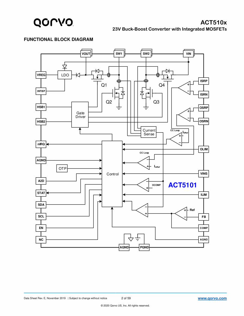
FUNCTIONAL BLOCK DIAGRAM
Q1
Q2 Q3
Q4
VINVOUT VOUTVIN
Gate Driver
LDOVREG
HSB2
A2D
AGND PGND
OLIM
SDA
SCL
AGND
STAT
SW1SW1 SW2SW2
nIRQ
Control
Current Sense
IORefCC Loop
ISRP
ISRN
FB
COMP
Ref
IinRef
CC Loop
EN
AGND
OSRP
OSRN
NC
OTP
HSB1
ACT5101
INTBP
ILIM
OCOMP
VINS
Data Sheet Rev. E, November 2019 | Subject to change without notice 3 of 59 www.qorvo.com
© 2020 Qorvo US, Inc. All rights reserved.
ACT510x
23V Buck-Boost Converter with Integrated MOSFETs
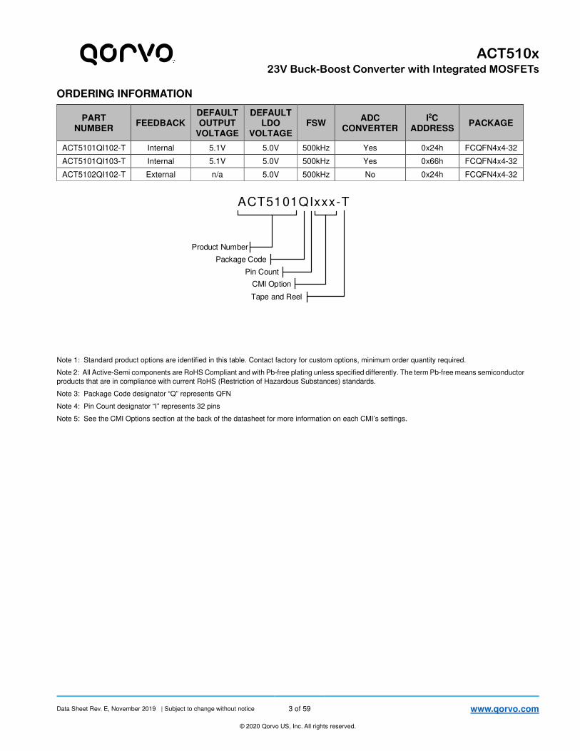
ORDERING INFORMATION
PART NUMBER
FEEDBACK DEFAULT OUTPUT
VOLTAGE
DEFAULT LDO
VOLTAGE FSW
ADC CONVERTER
I2C ADDRESS
PACKAGE
ACT5101QI102-T Internal 5.1V 5.0V 500kHz Yes 0x24h FCQFN4x4-32
ACT5101QI103-T Internal 5.1V 5.0V 500kHz Yes 0x66h FCQFN4x4-32
ACT5102QI102-T External n/a 5.0V 500kHz No 0x24h FCQFN4x4-32
ACT5101QIxxx-T
CMI Option
Pin Count
Package Code
Product Number
Tape and Reel
Note 1: Standard product options are identified in this table. Contact factory for custom options, minimum order quantity required.
Note 2: All Active-Semi components are RoHS Compliant and with Pb-free plating unless specified differently. The term Pb-free means semiconductor
products that are in compliance with current RoHS (Restriction of Hazardous Substances) standards.
Note 3: Package Code designator “Q” represents QFN
Note 4: Pin Count designator “I” represents 32 pins
Note 5: See the CMI Options section at the back of the datasheet for more information on each CMI’s settings.
Data Sheet Rev. E, November 2019 | Subject to change without notice 4 of 59 www.qorvo.com
© 2020 Qorvo US, Inc. All rights reserved.
ACT510x
23V Buck-Boost Converter with Integrated MOSFETs
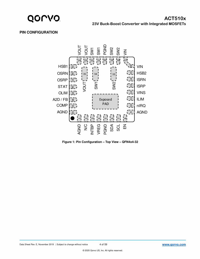
PIN CONFIGURATION
VINS
COMPP
GN
D
OSRN
OSRP
AGND
AG
ND
VR
EG
HSB1
N/C
INTB
P
VIN
HSB2
ISRN
AGND
nIRQ
EN
4321 765
11
15
OLIM 12
13
14
A2D / FB
8
ISRP
SC
L
SD
A
STAT
ILIM
32
31
29
30
28
Exposed
PAD
27
25
26
10
9
35 34 33
VO
UT
SW
1
SW
2
VO
UT
SW
2
SW
2
VO
UT
VIN
SW
1
SW
1
PG
ND
24 23 2122 20 19 1718 17
16
Figure 1: Pin Configuration – Top View – QFN4x4-32
Data Sheet Rev. E, November 2019 | Subject to change without notice 5 of 59 www.qorvo.com
© 2020 Qorvo US, Inc. All rights reserved.
ACT510x
23V Buck-Boost Converter with Integrated MOSFETs
PIN DESCRIPTIONS
PIN NAME DESCRIPTION
1, 9, 32 AGND Analog Ground. Kelvin connect AGND to the PGND plane.
2 NC No Connect. Connect this pin to AGND.
3 INTBP Internal Voltage Bypass - Connect a 100nF ceramic capacitor between INTBP and AGND
4 VREG Internal VREG LDO output. The output voltage is programmable from 2V to 5.1V. Connect a 1.0uF between VREG and AGND. The maximum current capability for this pin is 100mA.
5, 20 PGND Power Ground. Connect to large ground plane on PCB with thermal vias.
6 SDA I2C Data Input and Output. Needs an external pull up resistor.
7 SCL I2C Clock Input. Needs an external pull up resistor.
8 EN Enable Input. The converter is enabled when EN is pulled high and disabled when EN is pulled low.
10 nIRQ Interrupt Open-Drain Output. nIRQ goes low to indicate a fault condition. nIRQ is referenced to AGND.
11 ILIM Input current limit setting pin. Connect a resistor from ILIM to AGND to program the maximum input current.
12 VINS Input Voltage Sense Input – Kelvin connect to the input voltage input capacitors.
13 ISRP Input current sense resistor positive input.
14 ISRN Input current sense resistor negative input.
15 HSB2 High Side Bias Boot-strap pin. This provides power to the internal high-side MOSFET gate driver circuitry. Connect a 47nF capacitor from HSB2 to SW2 pin
16, 17 VIN Power Input pins. Connect these pins to 22uF-100uF ceramic capacitors placed as close to the IC as possible.
18, 19 SW2 Power switching output to external inductor.
21, 22 SW1 Power switching output to external inductor.
23, 24 VOUT Output voltage pins. Place 22uF to 44uF decoupling capacitors between VOUT and PGND.
25 HSB1 High Side Bias Boot-strap pin. This provides power to the internal high-side MOSFET gate driver circuitry. Connect a 47nF capacitor from HSB1 to SW1 pin
26 OSRN Output current sense resistor negative input
27 OSRP Output current sense resistor positive input.
28 STAT Open drain status output to indicate various IC operating conditions. A LOW indicates the converter is enabled and has a valid output. A HIZ indicates the converter is disabled for any reason
29 OLIM Output constant current limit setting pin. Connect a resistor from OLIM to AGND to program the output current.
30 (ACT5101)
A2D A2D input pin
30 (ACT5102)
FB Output voltage feedback pin.
31 COMP Error Amplifier Output. This pin is used to compensate the converter.
Exposed Pad
PGND Power Ground. Connect to large ground plane on PCB with thermal vias.
Data Sheet Rev. E, November 2019 | Subject to change without notice 6 of 59 www.qorvo.com
© 2020 Qorvo US, Inc. All rights reserved.
ACT510x
23V Buck-Boost Converter with Integrated MOSFETs
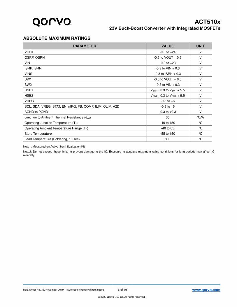
ABSOLUTE MAXIMUM RATINGS
PARAMETER VALUE UNIT
VOUT -0.3 to +24 V
OSRP, OSRN -0.3 to VOUT + 0.3 V
VIN -0.3 to +23 V
ISRP, ISRN -0.3 to VIN + 0.3 V
VINS -0.3 to ISRN + 0.3 V
SW1 -0.3 to VOUT + 0.3 V
SW2 -0.3 to VIN + 0.3 V
HSB1 VSW1 - 0.3 to VSW1 + 5.5 V
HSB2 VSW2 - 0.3 to VSW2 + 5.5 V
VREG -0.3 to +6 V
SCL, SDA, VREG, STAT, EN, nIRQ, FB, COMP, ILIM, OLIM, A2D -0.3 to +6 V
AGND to PGND -0.3 to +0.3 V
Junction to Ambient Thermal Resistance (θJA) 35 °C/W
Operating Junction Temperature (TJ) -40 to 150 °C
Operating Ambient Temperature Range (TA) -40 to 85 °C
Store Temperature -55 to 150 °C
Lead Temperature (Soldering, 10 sec) 300 °C
Note1: Measured on Active-Semi Evaluation Kit
Note2: Do not exceed these limits to prevent damage to the IC. Exposure to absolute maximum rating conditions for long periods may affect IC
reliability.
Data Sheet Rev. E, November 2019 | Subject to change without notice 7 of 59 www.qorvo.com
© 2020 Qorvo US, Inc. All rights reserved.
ACT510x
23V Buck-Boost Converter with Integrated MOSFETs
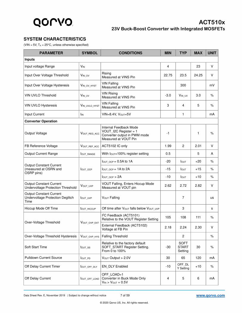
SYSTEM CHARACTERISTICS (VIN = 5V, TA = 25°C, unless otherwise specified)
PARAMETER SYMBOL CONDITIONS MIN TYP MAX UNIT
Inputs
Input voltage Range VIN 4 23 V
Input Over Voltage Threshold VIN_OV Rising Measured at VINS Pin
22.75 23.5 24.25 V
Input Over Voltage Hysteresis VIN_OV_HYST VIN Falling Measured at VINS Pin
300 mV
VIN UVLO Threshold VIN_UV VIN Rising Measured at VINS Pin
-3.0 VIN_UV 3.0 %
VIN UVLO Hysteresis VIN_UVLO_HYST VIN Falling Measured at VINS Pin
3 4 5 %
Input Current IIN VIN=8.4V, VOUT=5V 1 mA
Converter Operation
Output Voltage VOUT_REG_ACC
Internal Feedback Mode VOUT_I2C Register = 1 Converter output in PWM mode Measured at VOUT Pin
-1 1 %
FB Reference Voltage VOUT_REF_ACC ACT5102 IC only 1.99 2 2.01 V
Output Current Range IOUT_RANGE With IOUT=100% register setting 0.5 5 A
Output Constant Current (measured at OSRN and OSRP pins)
IOUT_OCP
IOUT_OCP = 0.5A to 1A -20 IOUT +20 %
IOUT_OCP = 1A to 2A -15 IOUT +15 %
IOUT_OCP > 2A -10 IOUT +10 %
Output Constant Current Undervoltage Protection Threshold
VOUT_UVP VOUT Falling, Enters Hiccup Mode Measured at VOUT pin
2.62 2.72 2.82 V
Output Constant Current Undervoltage Protection Deglitch Time
tOUT_UVP VOUT Falling 7 us
Hiccup Mode Off Time tOUT_HICCUP Off time after VOUT falls below VOUT_UVP 3 s
Over-Voltage Threshold VOUT_OVP_EXT
I2C Feedback (ACT5101) Relative to the VOUT Register Setting
105 108 111 %
External Feedback (ACT5102) Voltage at FB Pin
2.18 2.24 2.30 V
Over-Voltage Threshold Hysteresis VOUT_OVP_HYS Falling Threshold 2 %
Soft Start Time tOUT_SS Relative to the factory default SOFT_START Register Setting. From 0 to 100%
-30 SOFT
START Setting
30 %
Pulldown Current Source IOUT_PD VOUT Output > 2.0V 30 65 120 mA
Off Delay Current Timer tOUT_OFF_DLY EN_DLY Enabled -10 OFF_DL
Y Setting +10 %
Off Delay Current IOUT_OFF_LOAD OFF_LOAD=1 Converter in Buck Mode Only VIN > VOUT + 0.5V
4 5 6 mA
Data Sheet Rev. E, November 2019 | Subject to change without notice 8 of 59 www.qorvo.com
© 2020 Qorvo US, Inc. All rights reserved.
ACT510x
23V Buck-Boost Converter with Integrated MOSFETs
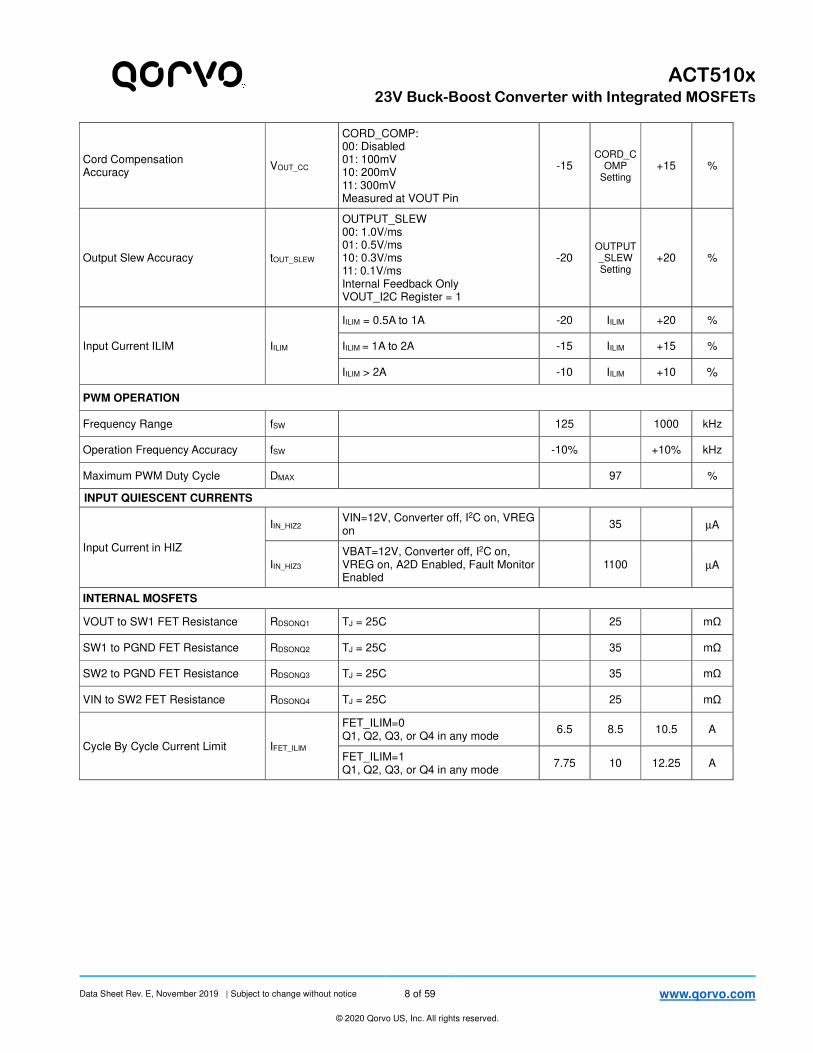
Cord Compensation Accuracy
VOUT_CC
CORD_COMP: 00: Disabled 01: 100mV 10: 200mV 11: 300mV Measured at VOUT Pin
-15 CORD_C
OMP Setting
+15 %
Output Slew Accuracy tOUT_SLEW
OUTPUT_SLEW 00: 1.0V/ms 01: 0.5V/ms 10: 0.3V/ms 11: 0.1V/ms Internal Feedback Only VOUT_I2C Register = 1
-20 OUTPUT_SLEW Setting
+20 %
Input Current ILIM IILIM
IILIM = 0.5A to 1A -20 IILIM +20 %
IILIM = 1A to 2A -15 IILIM +15 %
IILIM > 2A -10 IILIM +10 %
PWM OPERATION
Frequency Range fSW 125 1000 kHz
Operation Frequency Accuracy fSW -10% +10% kHz
Maximum PWM Duty Cycle DMAX 97 %
INPUT QUIESCENT CURRENTS
Input Current in HIZ
IIN_HIZ2 VIN=12V, Converter off, I2C on, VREG on
35 µA
IIN_HIZ3 VBAT=12V, Converter off, I2C on, VREG on, A2D Enabled, Fault Monitor Enabled
1100 µA
INTERNAL MOSFETS
VOUT to SW1 FET Resistance RDSONQ1 TJ = 25C 25 mΩ
SW1 to PGND FET Resistance RDSONQ2 TJ = 25C 35 mΩ
SW2 to PGND FET Resistance RDSONQ3 TJ = 25C 35 mΩ
VIN to SW2 FET Resistance RDSONQ4 TJ = 25C 25 mΩ
Cycle By Cycle Current Limit IFET_ILIM
FET_ILIM=0 Q1, Q2, Q3, or Q4 in any mode
6.5 8.5 10.5 A
FET_ILIM=1 Q1, Q2, Q3, or Q4 in any mode
7.75 10 12.25 A
Data Sheet Rev. E, November 2019 | Subject to change without notice 9 of 59 www.qorvo.com
© 2020 Qorvo US, Inc. All rights reserved.
ACT510x
23V Buck-Boost Converter with Integrated MOSFETs
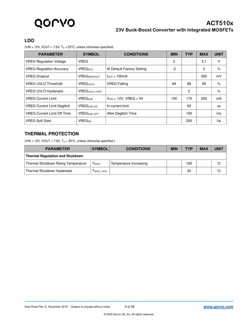
LDO
(VIN = 12V, VOUT = 7.6V, TA = 25°C, unless otherwise specified)
PARAMETER SYMBOL CONDITIONS MIN TYP MAX UNIT
VREG Regulation Voltage VREG 2 5.1 V
VREG Regulation Accuracy VREGACC At Default Factory Setting -2 2 %
VREG Dropout VREGDROPOUT IOUT = 100mA 300 mV
VREG UVLO Threshold VREGUVLO VREG Falling 84 88 93 %
VREG UVLO Hysteresis VREGUVLO_HYST 2 %
VREG Current Limit VREGILIM VVIN = 12V, VREG = 5V 100 175 250 mA
VREG Current Limit Deglitch VREGILIM_DG In current limit 50 us
VREG Current Limit Off Time VREGILIM_OFF After Deglitch Time 100 ms
VREG Soft Start VREGSS 250 Us
THERMAL PROTECTION
(VIN = 12V, VOUT = 7.6V, TA = 25°C, unless otherwise specified.)
PARAMETER SYMBOL CONDITIONS MIN TYP MAX UNIT
Thermal Regulation and Shutdown
Thermal Shutdown Rising Temperature TSHUT Temperature Increasing 160 °C
Thermal Shutdown Hysteresis TSHUT_HYS 30 °C
Data Sheet Rev. E, November 2019 | Subject to change without notice 10 of 59 www.qorvo.com
© 2020 Qorvo US, Inc. All rights reserved.
ACT510x
23V Buck-Boost Converter with Integrated MOSFETs
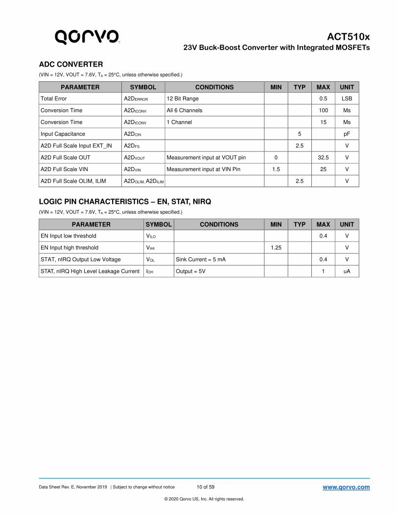
ADC CONVERTER
(VIN = 12V, VOUT = 7.6V, TA = 25°C, unless otherwise specified.)
PARAMETER SYMBOL CONDITIONS MIN TYP MAX UNIT
Total Error A2DERROR 12 Bit Range 0.5 LSB
Conversion Time A2DtCONV All 6 Channels 100 Ms
Conversion Time A2DtCONV 1 Channel 15 Ms
Input Capacitance A2DCIN 5 pF
A2D Full Scale Input EXT_IN A2DFS 2.5 V
A2D Full Scale OUT A2DVOUT Measurement input at VOUT pin 0 32.5 V
A2D Full Scale VIN A2DVIN Measurement input at VIN Pin 1.5 25 V
A2D Full Scale OLIM, ILIM A2DOLIM, A2DILIM 2.5 V
LOGIC PIN CHARACTERISTICS – EN, STAT, NIRQ
(VIN = 12V, VOUT = 7.6V, TA = 25°C, unless otherwise specified.)
PARAMETER SYMBOL CONDITIONS MIN TYP MAX UNIT
EN Input low threshold VILO 0.4 V
EN Input high threshold VIHI 1.25 V
STAT, nIRQ Output Low Voltage VOL Sink Current = 5 mA 0.4 V
STAT, nIRQ High Level Leakage Current IOH Output = 5V 1 uA
Data Sheet Rev. E, November 2019 | Subject to change without notice 11 of 59 www.qorvo.com
© 2020 Qorvo US, Inc. All rights reserved.
ACT510x
23V Buck-Boost Converter with Integrated MOSFETs
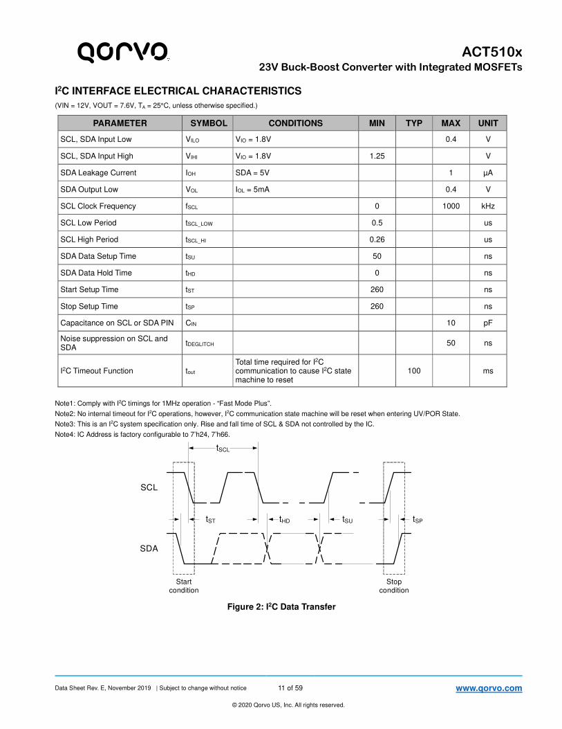
I2C INTERFACE ELECTRICAL CHARACTERISTICS
(VIN = 12V, VOUT = 7.6V, TA = 25°C, unless otherwise specified.)
PARAMETER SYMBOL CONDITIONS MIN TYP MAX UNIT
SCL, SDA Input Low VILO VIO = 1.8V 0.4 V
SCL, SDA Input High VIHI VIO = 1.8V 1.25 V
SDA Leakage Current IOH SDA = 5V 1 µA
SDA Output Low VOL IOL = 5mA 0.4 V
SCL Clock Frequency fSCL 0 1000 kHz
SCL Low Period tSCL_LOW 0.5 us
SCL High Period tSCL_HI 0.26 us
SDA Data Setup Time tSU 50 ns
SDA Data Hold Time tHD 0 ns
Start Setup Time tST 260 ns
Stop Setup Time tSP 260 ns
Capacitance on SCL or SDA PIN CIN 10 pF
Noise suppression on SCL and SDA
tDEGLITCH 50 ns
I2C Timeout Function tout Total time required for I2C communication to cause I2C state machine to reset
100 ms
Note1: Comply with I2C timings for 1MHz operation - “Fast Mode Plus”.
Note2: No internal timeout for I2C operations, however, I2C communication state machine will be reset when entering UV/POR State.
Note3: This is an I2C system specification only. Rise and fall time of SCL & SDA not controlled by the IC.
Note4: IC Address is factory configurable to 7’h24, 7’h66.
Figure 2: I2C Data Transfer
SDA
SCL
tST tSUtHD tSP
tSCL
Start condition
Stop condition
Data Sheet Rev. E, November 2019 | Subject to change without notice 12 of 59 www.qorvo.com
© 2020 Qorvo US, Inc. All rights reserved.
ACT510x
23V Buck-Boost Converter with Integrated MOSFETs
FUNCTIONAL DESCRIPTION
General
ACT510x is a buck-boost converter with integrated
MOSFETs. It provides a high efficiency, low external
component count, minimal size buck-boost power
solution. Its wide input operating range of 3.9V to 23V
allows operation from many input sources. The
ACT5101 output voltage is set by internal registers. It
has a built in A/D converter. The ACT5102 output
voltage is set by an external resistor divider and does
not have an A/D converter.
The ACT510x autonomously switches between buck,
buck-boost, and boost modes depending on the input
and output voltages. It is optimized for minimum
quiescent current in shutdown and standby modes. This
makes it ideal for battery powered applications.
The ACT510x can be operated in both stand-alone and
host-controlled applications. External resistors set the
input and output current limit. Using host controlled I2C
operation, the user has full control over voltage, current,
and fault settings.
I2C operation gives the host full control of operating
parameters as well as full knowledge of the operating
parameters and fault conditions. A built in ADC provides
input voltage, output voltage, input current, output
current, and die temperature. The ADC also has one
general purpose input to measure an external analog
signal.
The ACT510x is highly flexible and contains many I2C
configurable functions. The IC’s default functionality is
defined by its default CMI (Code Matrix Index), but
much of this functionality can be changed via I2C. I2C
functionality includes OV and UV fault thresholds,
switching frequencies, current limits, output voltage,
slew rates, softstart time, and more. The CMI Options
section shows the default settings for each available
CMI option. Contact [email protected] for
additional information about other configurations.
I2C Serial Interface
To ensure compatibility with a wide range of systems,
the ACT510x uses standard I2C commands. It supports
clock speeds up to 1MHz. The ACT510x always
operates as a slave device, and can be factory
configured to one of two 7-bit slave addresses. The
7-bit slave address is followed by an eighth bit, which
indicates whether the transaction is a read-operation or
a write-operation. Refer to each specific CMI for the IC’s
slave address
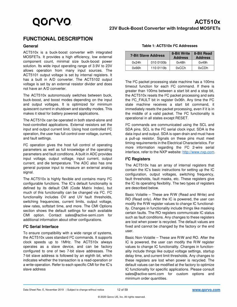
Table 1: ACT510x I2C Addresses
7-Bit Slave Address 8-Bit Write Address
8-Bit Read Address
0x24h 010 0100b 0x48h 0x49h
0x66h 110 0110b 0xCCh 0xCDh
The I2C packet processing state machine has a 100ms
timeout function for each I2C command. If there is
greater than 100ms between a start bit and a stop bit,
the ACT510x resets the I2C packet processing and sets
the I2C_FAULT bit in register 0x06h. Any time the I2C
state machine receives a start bit command, it
immediately resets the packet processing, even if it is in
the middle of a valid packet. The I2C functionality is
operational in all states except RESET.
I2C commands are communicated using the SCL and
SDA pins. SCL is the I2C serial clock input. SDA is the
data input and output. SDA is open drain and must have
a pull-up resistor. Signals on these pins must meet
timing requirements in the Electrical Characteristics. For
more information regarding the I2C 2-wire serial
interface, refer to the NXP website: http://www.nxp.com.
I2C Registers
The ACT510x has an array of internal registers that
contain the IC’s basic instructions for setting up the IC
configuration, output voltages, switching frequency,
fault thresholds, fault masks, etc. These registers give
the IC its operating flexibility. The two types of registers
are described below.
Basic Volatile – These are R/W (Read and Write) and
RO (Read only). After the IC is powered, the user can
modify the R/W register values to change IC functional-
ity. Changes in functionality include things like masking
certain faults. The RO registers communicate IC status
such as fault conditions. Any changes to these registers
are lost when power is recycled. The default values are
fixed and cannot be changed by the factory or the end
user.
Basic Non-Volatile – These are R/W and RO. After the
IC is powered, the user can modify the R/W register
values to change IC functionality. Changes in function-
ality include things like output voltage settings, startup
delay time, and current limit thresholds. Any changes to
these registers are lost when power is recycled. The
default values can be modified at the factory to optimize
IC functionality for specific applications. Please consult
[email protected] for custom options and
minimum order quantities.
Data Sheet Rev. E, November 2019 | Subject to change without notice 13 of 59 www.qorvo.com
© 2020 Qorvo US, Inc. All rights reserved.
ACT510x
23V Buck-Boost Converter with Integrated MOSFETs
When modifying only certain bits within a register, take
care to not inadvertently change other bits. Inadvert-
ently changing register contents can lead to unexpected
IC behavior.
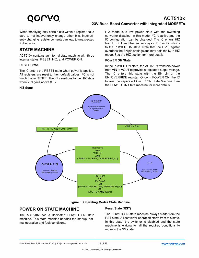
STATE MACHINE
ACT510x contains an internal state machine with three
internal states: RESET, HIZ, and POWER ON.
RESET State
The IC enters the RESET state when power is applied.
All registers are reset to their default values. I2C is not
functional in RESET. The IC transitions to the HIZ state
when VIN goes above 3.9V
HIZ State
HIZ mode is a low power state with the switching
converter disabled. In this mode, I2C is active and the
IC configuration can be changed. The IC enters HIZ
from RESET and then either stays in HIZ or transitions
to the POWER ON state. Note that the HIZ Register
overrides the EN pin settings and may hold the IC in HIZ
mode. See the HIZ section for more details.
POWER ON State
In the POWER ON state, the ACT510x transfers power
from VIN to VOUT to provide a regulated output voltage.
The IC enters this state with the EN pin or the
EN_OVERRIDE register. Once in POWER ON, the IC
follows the separate POWER ON State Machine. See
the POWER ON State machine for more details.
Figure 3: Operating Modes State Machine
POWER ON STATE MACHINE
The ACT510x has a dedicated POWER ON state
machine. This state machine handles the startup, nor-
mal operation and fault conditions.
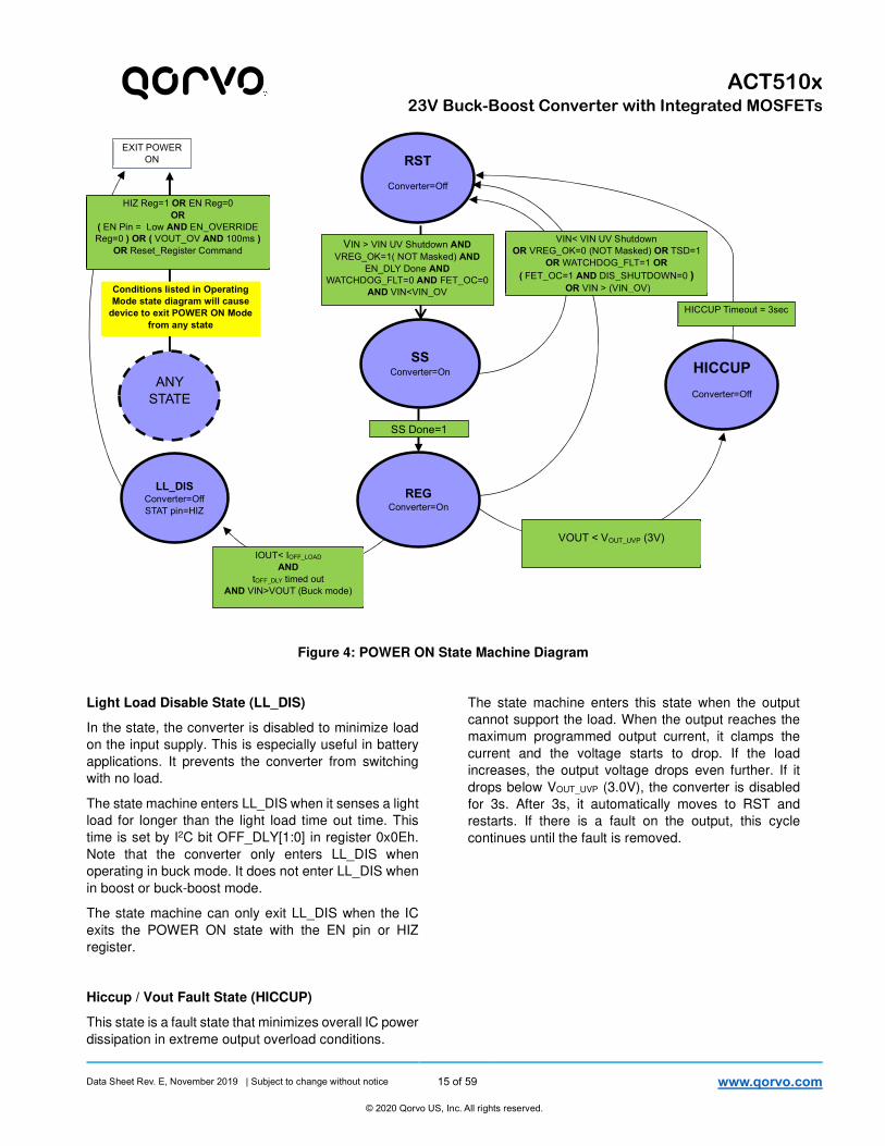
Reset State (RST)
The POWER ON state machine always starts from the
RST state. All converter operation starts from this state.
In this state, the switcher is disabled and the state
machine is waiting for all the required conditions to
move to the SS state.
HIZ
Converter=DISABLED
VREG=VREG_DIS REG
POWER ON
Converter=ENABLED
VREG=VREG_DIS REG
RESET
Input Power applied and
all registers reset to
defaults
HIZ Reg=0
AND
EN Reg=1
AND
( EN Pin = HI OR EN_OVERRIDE Reg=1 )
HIZ Reg=1
OR
EN Reg=0
OR
(EN Pin = LOW AND EN_OVERRIDE Reg=0)
OR
(VOUT_OV AND 100ms)
(VIN Pin <1V AND VOUT Pin<1V) VIN Pin > 3.9V
Data Sheet Rev. E, November 2019 | Subject to change without notice 14 of 59 www.qorvo.com
© 2020 Qorvo US, Inc. All rights reserved.
ACT510x
23V Buck-Boost Converter with Integrated MOSFETs
After all the following fault conditions are cleared, the IC
starts the Enable Delay Timer. This timer is controlled
by I2C bit EN_DLY[1:0] in register 0x0Fh. Once the timer
has expired, the state machine moves to the SS state.
Reset Faults:
VIN UV Shutdown voltage: This fault is active when
the input voltage is lower than the programmed VIN UV
Shutdown voltage. This shutdown voltage is set by two
I2C registers: VIN_UV in register 0x0Fh and
VIN_UV_OFFSET in register 0x1Ah. The actual
shutdown voltage is equal to the programmed
VIN_UV_OFFSET voltage minus the programmed
VIN_UV voltage. This fault self-clears when VIN is
higher than the UV Shutdown voltage.
VREG LDO OK – This fault is set when an LDO fault is
detected. This includes the 100msec timeout period.
This fault automatically clears when the VREG LDO has
exited the faulted condition. Note: This fault can be
masked to allow the state machine to exit RST while
there is a fault on the VREG LDO by using the I2C bit
DIS_VREG_FLT in register 0x10 Bit 1.
Watchdog Timer Fault: This fault is active if the watch-
dog timer is enabled and the timer times out. This fault
clears when the watchdog timer is reset or cleared. It
can be reset by writing a 1 into the I2C bit WATCH-
DOG_RESET in register 0x00h. It can be cleared by
disabling the watchdog timer by setting I2C bits
WATCHDOG[1:0] = 0x00h.
FET Overcurrent Fault: This fault is set if a switching
FET exceeds the cycle-by-cycle current limit for 8 (or 16)
consecutive cycles. The FET_OC fault is latched. To
clear this latch, the IC must exit the POWER ON state
and enter HIZ mode. This is typically accomplished by
toggling the EN pin or setting the HIZ register to 1.
VIN Overvoltage: This fault is set if VIN exceeds the
VVIN_OV voltage, 23.5V. The OV fault self-clears when
VIN drops below VVIN_OV and the IC exits the RST state.
Die Thermal Shutdown (TSD): This fault is active
when die temperature exceeds the TSHUT (160°C)
temperature. This fault self-clears when the die
temperature cools down by the temperature hysteresis,
TSHUT_HYST (30°C). This fault cannot be cleared or
masked. The IC must cool down before exiting the RST
state.
Softstart State (SS)
In this state, the IC enables the converter and softstarts
the output voltage.
The state machine enters the SS state from the RST
state when all faults are cleared. The state machine
transitions to the REG state after the output is
softstarted an in regulation.
The softstart time is controllable by the I2C bit SS in reg-
ister 0x0Eh. If a fault occurs during the softstart, the
state machine jumps back to the RST state and disables
the converter. Once the soft start is done, the IC jumps
to the REG state.
Regulation State (REG)
The normal regulation occurs in the REG state. If a
major fault occurs during operation the IC will jump back
to the reset state and disable the converter. During this
state, the converter can be disabled with a light load
condition. Additionally, if the output drops below
VOUT_UVP (3.0V), the IC will go into a hiccup mode to
protect the output in a shorted condition.
Data Sheet Rev. E, November 2019 | Subject to change without notice 15 of 59 www.qorvo.com
© 2020 Qorvo US, Inc. All rights reserved.
ACT510x
23V Buck-Boost Converter with Integrated MOSFETs
Figure 4: POWER ON State Machine Diagram
Light Load Disable State (LL_DIS)
In the state, the converter is disabled to minimize load
on the input supply. This is especially useful in battery
applications. It prevents the converter from switching
with no load.
The state machine enters LL_DIS when it senses a light
load for longer than the light load time out time. This
time is set by I2C bit OFF_DLY[1:0] in register 0x0Eh.
Note that the converter only enters LL_DIS when
operating in buck mode. It does not enter LL_DIS when
in boost or buck-boost mode.
The state machine can only exit LL_DIS when the IC
exits the POWER ON state with the EN pin or HIZ
register.
Hiccup / Vout Fault State (HICCUP)
This state is a fault state that minimizes overall IC power
dissipation in extreme output overload conditions.
The state machine enters this state when the output
cannot support the load. When the output reaches the
maximum programmed output current, it clamps the
current and the voltage starts to drop. If the load
increases, the output voltage drops even further. If it
drops below VOUT_UVP (3.0V), the converter is disabled
for 3s. After 3s, it automatically moves to RST and
restarts. If there is a fault on the output, this cycle
continues until the fault is removed.
SS Converter=On
IOUT< IOFF_LOAD
AND
tOFF_DLY timed out
AND VIN>VOUT (Buck mode)
RST
Converter=Off
HICCUP Timeout = 3sec
ANY
STATE
EXIT POWER
ON
Conditions listed in Operating
Mode state diagram will cause
device to exit POWER ON Mode
from any state
HICCUP
Converter=Off
VIN > VIN UV Shutdown AND
VREG_OK=1( NOT Masked) AND
EN_DLY Done AND
WATCHDOG_FLT=0 AND FET_OC=0
AND VIN<VIN_OV
REG Converter=On
VIN< VIN UV Shutdown
OR VREG_OK=0 (NOT Masked) OR TSD=1
OR WATCHDOG_FLT=1 OR
( FET_OC=1 AND DIS_SHUTDOWN=0 ) OR VIN > (VIN_OV)
VOUT < VOUT_UVP (3V)
LL_DIS Converter=Off
STAT pin=HIZ
SS Done=1
HIZ Reg=1 OR EN Reg=0
OR
( EN Pin = Low AND EN_OVERRIDE
Reg=0 ) OR ( VOUT_OV AND 100ms )
OR Reset_Register Command
Data Sheet Rev. E, November 2019 | Subject to change without notice 16 of 59 www.qorvo.com
© 2020 Qorvo US, Inc. All rights reserved.
ACT510x
23V Buck-Boost Converter with Integrated MOSFETs
PIN FUNCTIONS
VIN
VIN is the ACT510x input power pin. Input voltage
sensing is measured at the VIN pin. Connect input
bypass capacitors directly between VIN and PGND.
ISRP
ISRP is the positive sense pin for input current sensing.
ISRP requires an input RC filter. Refer to the Input
Current Regulation section for more details. ISRP
must be Kelvin connected to the input current sense
resistor. Connect the input current sense resistor
between ISRP and ISRN.
ISRN
ISRN is the negative sense pin for input current sensing.
ISRN requires an input RC filter. Refer to the Input
Current Regulation section for more details. ISRN
must be Kelvin connected to the input current sense
resistor. Connect the input current sense resistor
between ISRP and ISRN.
SW1, SW2
SW1 and SW2 are the switch nodes for the internal
buck-boost converter. SW1 switches between VOUT
and PGND when the IC operates in buck-boost and
boost modes. SW2 switches between VIN and PGND
when the IC operates in buck and buck-boost modes.
Connect the inductor between the SW1 and SW2 pins.
HSB1, HSB2
HSB1 and HSB2 provide power to the internal high-side
MOSFET gate driver circuitry. Connect a 47nF
capacitor from HSB1 to SW1. Connect a 47nF capacitor
from HSB2 to SW2.
VOUT
VOUT is the ACT510x output power pin. Connect output
bypass capacitors directly between VOUT and PGND.
VINS
VINS is the input voltage sense pin. Kelvin connect
input VINS to the input bypass capacitors.
OSRP
OSRP is the positive sense pin for the output current.
OSRP requires an input RC filter. Refer to the Setting
Maximum Output Current section for more details.
OSRP must be Kelvin connected to the output current
sense resistor. Connect the output current sense
resistor between OSRP and OSRN.
OSRN
OSRN is the negative sense pin for the output current.
OSRN requires an input RC filter. Refer to the Setting
Maximum Output Current section for more details.
OSRN must be Kelvin connected to the output current
sense resistor. Connect the output current sense
resistor between OSRP and OSRN.
ILIM
ILIM sets the maximum input current. Connect a resistor
between ILIM and AGND to set the current limits. The
ILIM current limit can be scaled using I2C. In some
operating conditions, ILIM requires additional RC
compensation. Refer to the Input Current Regulation
section for more details.
OLIM
OLIM sets the maximum output current. Connect a
resistor between OLIM and AGND to set the output
current limit. The OLIM current limit can be scaled using
I2C. In some operating conditions, OLIM requires
additional RC compensation. Refer to the Setting
Maximum Output Current section for more details.
INTBP
INTBP is the internal bias voltage output pin. INTBP is
supplied by an internal linear regulator. Do not power
external circuity from the INTBP pin. Connect a 100nF
ceramic capacitor between INTBP and AGND.
VREG
VREG is the internal LDO output pin. The internal LDO
is programmable between 2V and 5.1V. Its maximum
output current capability 100mA. Connect a 1uF
ceramic capacitor between VREG and AGND
EN
EN is the active high enable input. Pulling EN high
enables the converter. The EN polarity is configurable
via NVM to make it active low or active high. Active high
is the default. EN is 5V compliant.
STAT
STAT is an open drain status pin. It indicates the state
of the converter. It goes low to indicate the converter is
enabled and has a valid output voltage. It goes HIZ to
indicate the converter is disabled or that the converter
is enabled but in a fault condition.
Data Sheet Rev. E, November 2019 | Subject to change without notice 17 of 59 www.qorvo.com
© 2020 Qorvo US, Inc. All rights reserved.
ACT510x
23V Buck-Boost Converter with Integrated MOSFETs
Table 2: STAT Pin State
State STAT Output Pin
Output Enabled and Output Valid LOW
Output Disabled HIZ
Output Enabled In Fault, Hiccup, or Light Load states
HIZ
COMP
COMP is the converter compensation pin. Connect the
compensation components between COMP and AGND.
See the Compensation section for details.
A2D/FB
This is a dual function pin. It is an A2D input for the
ACT510x. Connect this pin directly to the voltage to be
measured. Note that the ADC full scale input voltage is
2.5V. It is the output voltage feedback pin for the
ACT5102.
nIRQ
ACT510x has an interrupt pin to inform the host of any
fault conditions. In general, any IC function with a status
bit asserts nIRQ pin low if the status changes. The
status changes can be masked by setting their
corresponding register bits. If nIRQ is asserted low, the
fault must be read before the IC deasserts nIRQ. If the
fault remains after reading the status bits, nIRQ remains
asserted. Refer to the nIRQ Interrupt Pin (nIRQ)
section for more details.
nIRQ is an open-drain output and should be pulled up
to an appropriate supply voltage with a 10kΩ or greater
pull-up resistor. nIRQ is 5V compliant
SCL, SDA
SCL and SDA are the I2C clock and data pins to the IC
They have standard I2C functionality. They are open-
drain outputs and each require a pull-up resistor. The
pull-up resistor is typically tied to the system’s uP IO
pins. The pullup voltage can range from 1.8V to 5.0V.
SCL and SDA are open drain and are 5V compliant.
NC
This pin is not used and should be connected directly to
AGND
PGND
The PGND pin is the buck-boost converters’ power
ground. The internal FETs connect directly to the PGND
pins. The power supply input and output capacitors
must connect to the PGND pins.
AGND
The AGND pin is the IC’s analog ground pin. It is a “quiet”
ground pin that is separate and isolated from the high
power, high current carrying PGND ground plane.
Connect the non-power components to AGND. AGND
must be Kelvin connected to the PGND pin in a single
location.
Exposed PAD
The Exposed pad is connected directly to the PGND
pins and must be soldered to the top side ground plane.
Place thermal vias under the Exposed PAD to improve
the IC’s thermal performance.
Data Sheet Rev. E, November 2019 | Subject to change without notice 18 of 59 www.qorvo.com
© 2020 Qorvo US, Inc. All rights reserved.
ACT510x
23V Buck-Boost Converter with Integrated MOSFETs
BUCK-BOOST OPERATION
The ACT510x is a monolithic buck-boost converter.
Four internal, low resistance, NMOS switches minimize
the application circuit size and reduce power losses to
maximize efficiency. Internal high side gate drivers,
which require only two small external capacitors, further
simplify the design process. An advanced switch control
algorithm allows the buck-boost converter to maintain
constant output voltage regulation with input voltages
that are above, equal to, or below the regulated output
voltage. The ACT510x automatically transitions
between these three operating modes, depending on
the input to output voltage ratios.
Power Stage
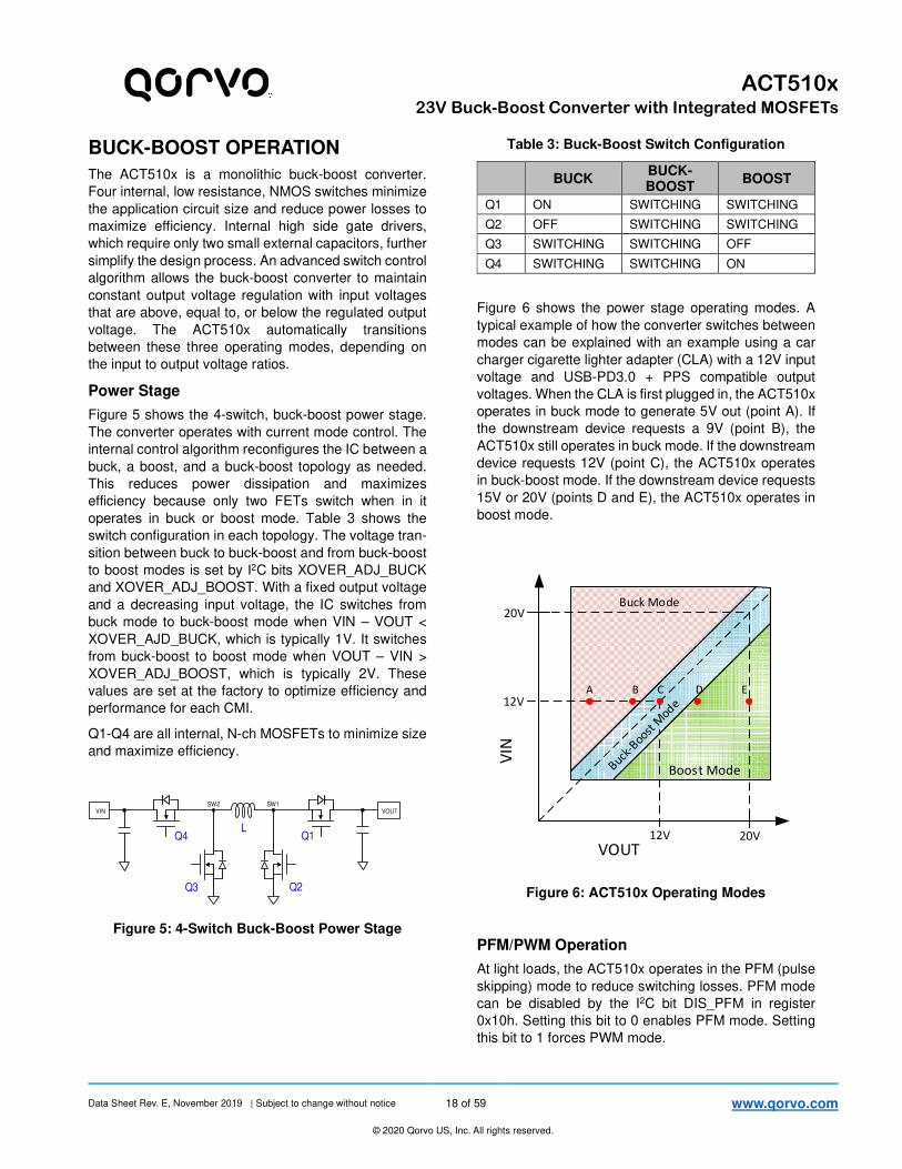
Figure 5 shows the 4-switch, buck-boost power stage.
The converter operates with current mode control. The
internal control algorithm reconfigures the IC between a
buck, a boost, and a buck-boost topology as needed.
This reduces power dissipation and maximizes
efficiency because only two FETs switch when in it
operates in buck or boost mode. Table 3 shows the
switch configuration in each topology. The voltage tran-
sition between buck to buck-boost and from buck-boost
to boost modes is set by I2C bits XOVER_ADJ_BUCK
and XOVER_ADJ_BOOST. With a fixed output voltage
and a decreasing input voltage, the IC switches from
buck mode to buck-boost mode when VIN – VOUT <
XOVER_AJD_BUCK, which is typically 1V. It switches
from buck-boost to boost mode when VOUT – VIN >
XOVER_ADJ_BOOST, which is typically 2V. These
values are set at the factory to optimize efficiency and
performance for each CMI.
Q1-Q4 are all internal, N-ch MOSFETs to minimize size
and maximize efficiency.
VIN
Q4
Q3 Q2
Q1
VOUT
L
SW2 SW1
Figure 5: 4-Switch Buck-Boost Power Stage
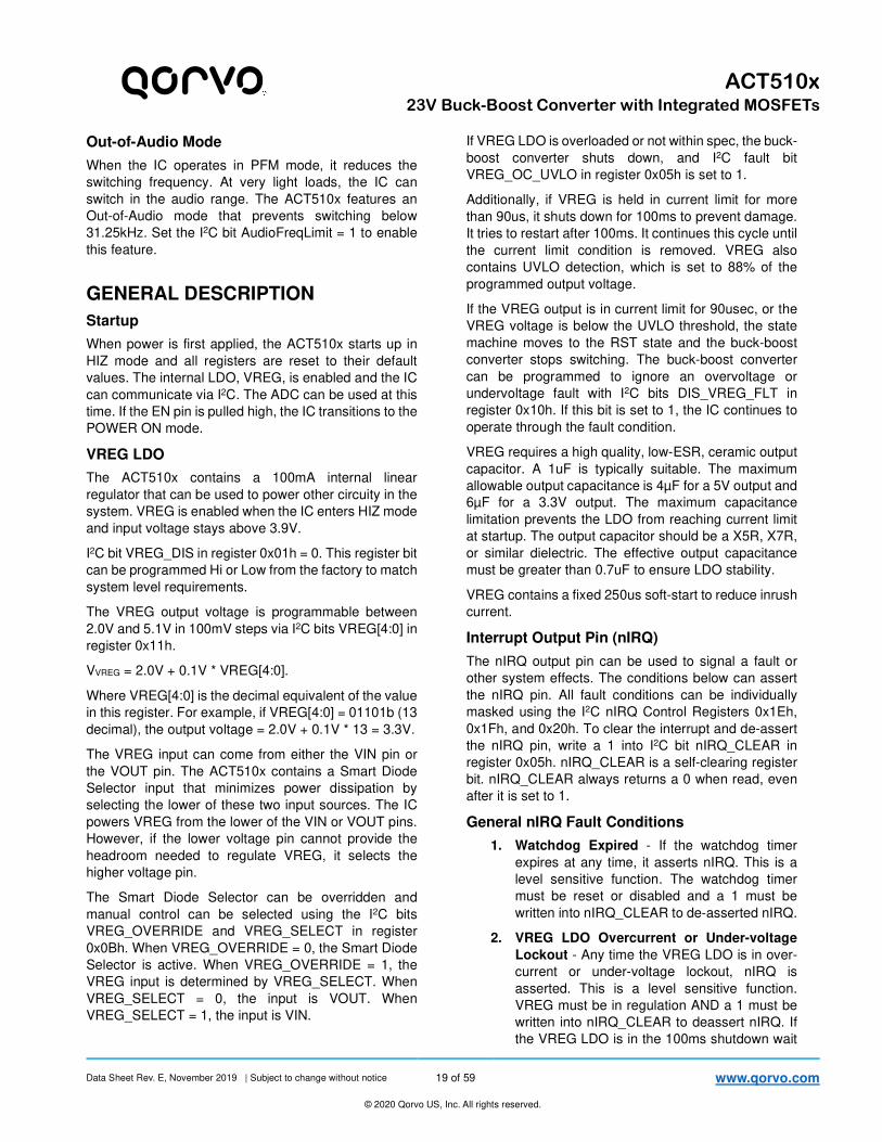
Table 3: Buck-Boost Switch Configuration
BUCK BUCK-BOOST
BOOST
Q1 ON SWITCHING SWITCHING
Q2 OFF SWITCHING SWITCHING
Q3 SWITCHING SWITCHING OFF
Q4 SWITCHING SWITCHING ON
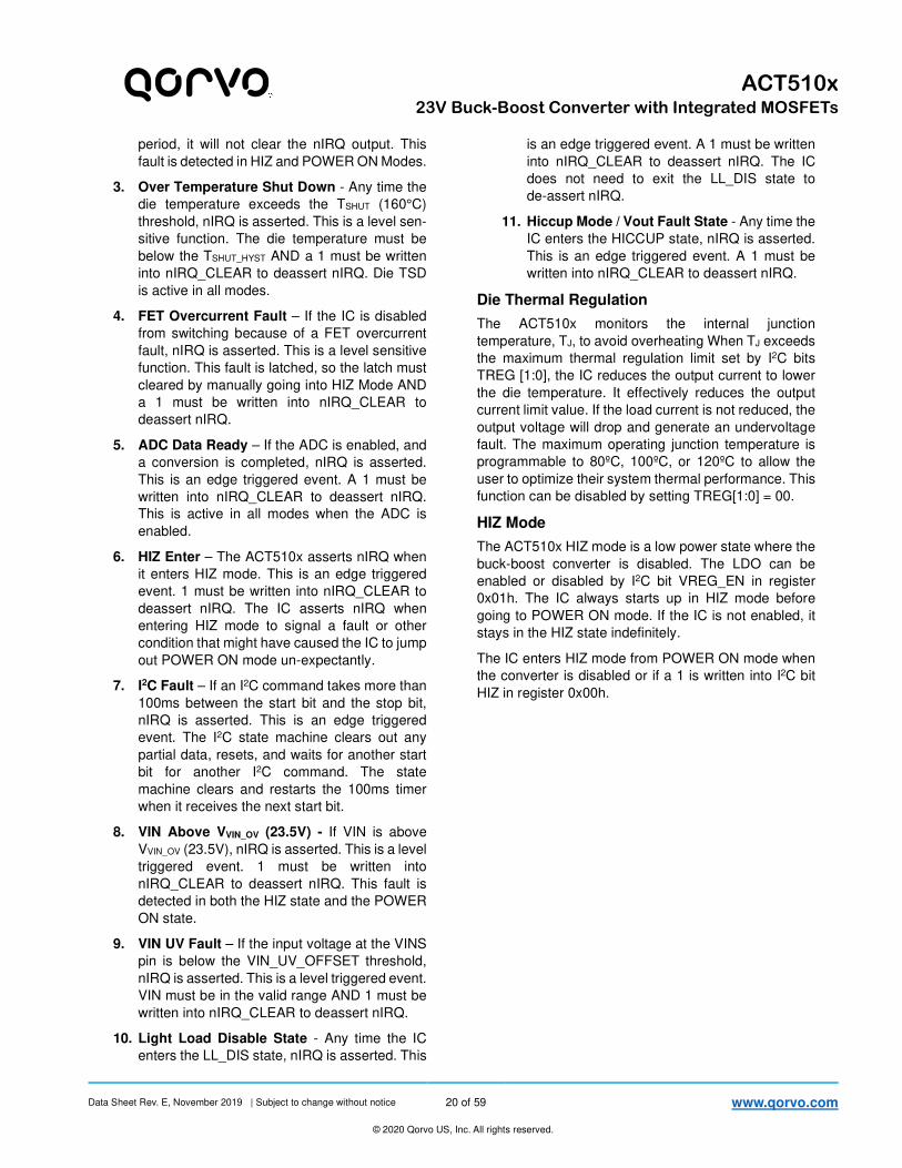
Figure 6 shows the power stage operating modes. A
typical example of how the converter switches between
modes can be explained with an example using a car
charger cigarette lighter adapter (CLA) with a 12V input
voltage and USB-PD3.0 + PPS compatible output
voltages. When the CLA is first plugged in, the ACT510x
operates in buck mode to generate 5V out (point A). If
the downstream device requests a 9V (point B), the
ACT510x still operates in buck mode. If the downstream
device requests 12V (point C), the ACT510x operates
in buck-boost mode. If the downstream device requests
15V or 20V (points D and E), the ACT510x operates in
boost mode.
20V
12V
12V 20V
VOUT
VIN
Buck Mode
Boost Mode
A B C D E
Figure 6: ACT510x Operating Modes
PFM/PWM Operation
At light loads, the ACT510x operates in the PFM (pulse
skipping) mode to reduce switching losses. PFM mode
can be disabled by the I2C bit DIS_PFM in register
0x10h. Setting this bit to 0 enables PFM mode. Setting
this bit to 1 forces PWM mode.
Data Sheet Rev. E, November 2019 | Subject to change without notice 19 of 59 www.qorvo.com
© 2020 Qorvo US, Inc. All rights reserved.
ACT510x
23V Buck-Boost Converter with Integrated MOSFETs
Out-of-Audio Mode
When the IC operates in PFM mode, it reduces the
switching frequency. At very light loads, the IC can
switch in the audio range. The ACT510x features an
Out-of-Audio mode that prevents switching below
31.25kHz. Set the I2C bit AudioFreqLimit = 1 to enable
this feature.
GENERAL DESCRIPTION
Startup
When power is first applied, the ACT510x starts up in
HIZ mode and all registers are reset to their default
values. The internal LDO, VREG, is enabled and the IC
can communicate via I2C. The ADC can be used at this
time. If the EN pin is pulled high, the IC transitions to the
POWER ON mode.
VREG LDO
The ACT510x contains a 100mA internal linear
regulator that can be used to power other circuity in the
system. VREG is enabled when the IC enters HIZ mode
and input voltage stays above 3.9V.
I2C bit VREG_DIS in register 0x01h = 0. This register bit
can be programmed Hi or Low from the factory to match
system level requirements.
The VREG output voltage is programmable between
2.0V and 5.1V in 100mV steps via I2C bits VREG[4:0] in
register 0x11h.
VVREG = 2.0V + 0.1V * VREG[4:0].
Where VREG[4:0] is the decimal equivalent of the value
in this register. For example, if VREG[4:0] = 01101b (13
decimal), the output voltage = 2.0V + 0.1V * 13 = 3.3V.
The VREG input can come from either the VIN pin or
the VOUT pin. The ACT510x contains a Smart Diode
Selector input that minimizes power dissipation by
selecting the lower of these two input sources. The IC
powers VREG from the lower of the VIN or VOUT pins.
However, if the lower voltage pin cannot provide the
headroom needed to regulate VREG, it selects the
higher voltage pin.
The Smart Diode Selector can be overridden and
manual control can be selected using the I2C bits
VREG_OVERRIDE and VREG_SELECT in register
0x0Bh. When VREG_OVERRIDE = 0, the Smart Diode
Selector is active. When VREG_OVERRIDE = 1, the
VREG input is determined by VREG_SELECT. When
VREG_SELECT = 0, the input is VOUT. When
VREG_SELECT = 1, the input is VIN.
If VREG LDO is overloaded or not within spec, the buck-
boost converter shuts down, and I2C fault bit
VREG_OC_UVLO in register 0x05h is set to 1.
Additionally, if VREG is held in current limit for more
than 90us, it shuts down for 100ms to prevent damage.
It tries to restart after 100ms. It continues this cycle until
the current limit condition is removed. VREG also
contains UVLO detection, which is set to 88% of the
programmed output voltage.
If the VREG output is in current limit for 90usec, or the
VREG voltage is below the UVLO threshold, the state
machine moves to the RST state and the buck-boost
converter stops switching. The buck-boost converter
can be programmed to ignore an overvoltage or
undervoltage fault with I2C bits DIS_VREG_FLT in
register 0x10h. If this bit is set to 1, the IC continues to
operate through the fault condition.
VREG requires a high quality, low-ESR, ceramic output
capacitor. A 1uF is typically suitable. The maximum
allowable output capacitance is 4µF for a 5V output and
6µF for a 3.3V output. The maximum capacitance
limitation prevents the LDO from reaching current limit
at startup. The output capacitor should be a X5R, X7R,
or similar dielectric. The effective output capacitance
must be greater than 0.7uF to ensure LDO stability.
VREG contains a fixed 250us soft-start to reduce inrush
current.
Interrupt Output Pin (nIRQ)
The nIRQ output pin can be used to signal a fault or
other system effects. The conditions below can assert
the nIRQ pin. All fault conditions can be individually
masked using the I2C nIRQ Control Registers 0x1Eh,
0x1Fh, and 0x20h. To clear the interrupt and de-assert
the nIRQ pin, write a 1 into I2C bit nIRQ_CLEAR in
register 0x05h. nIRQ_CLEAR is a self-clearing register
bit. nIRQ_CLEAR always returns a 0 when read, even
after it is set to 1.
General nIRQ Fault Conditions
1. Watchdog Expired - If the watchdog timer
expires at any time, it asserts nIRQ. This is a
level sensitive function. The watchdog timer
must be reset or disabled and a 1 must be
written into nIRQ_CLEAR to de-asserted nIRQ.
2. VREG LDO Overcurrent or Under-voltage
Lockout - Any time the VREG LDO is in over-
current or under-voltage lockout, nIRQ is
asserted. This is a level sensitive function.
VREG must be in regulation AND a 1 must be
written into nIRQ_CLEAR to deassert nIRQ. If
the VREG LDO is in the 100ms shutdown wait
Data Sheet Rev. E, November 2019 | Subject to change without notice 20 of 59 www.qorvo.com
© 2020 Qorvo US, Inc. All rights reserved.
ACT510x
23V Buck-Boost Converter with Integrated MOSFETs
period, it will not clear the nIRQ output. This
fault is detected in HIZ and POWER ON Modes.
3. Over Temperature Shut Down - Any time the
die temperature exceeds the TSHUT (160°C)
threshold, nIRQ is asserted. This is a level sen-
sitive function. The die temperature must be
below the TSHUT_HYST AND a 1 must be written
into nIRQ_CLEAR to deassert nIRQ. Die TSD
is active in all modes.
4. FET Overcurrent Fault – If the IC is disabled
from switching because of a FET overcurrent
fault, nIRQ is asserted. This is a level sensitive
function. This fault is latched, so the latch must
cleared by manually going into HIZ Mode AND
a 1 must be written into nIRQ_CLEAR to
deassert nIRQ.
5. ADC Data Ready – If the ADC is enabled, and
a conversion is completed, nIRQ is asserted.
This is an edge triggered event. A 1 must be
written into nIRQ_CLEAR to deassert nIRQ.
This is active in all modes when the ADC is
enabled.
6. HIZ Enter – The ACT510x asserts nIRQ when
it enters HIZ mode. This is an edge triggered
event. 1 must be written into nIRQ_CLEAR to
deassert nIRQ. The IC asserts nIRQ when
entering HIZ mode to signal a fault or other
condition that might have caused the IC to jump
out POWER ON mode un-expectantly.
7. I2C Fault – If an I2C command takes more than
100ms between the start bit and the stop bit,
nIRQ is asserted. This is an edge triggered
event. The I2C state machine clears out any
partial data, resets, and waits for another start
bit for another I2C command. The state
machine clears and restarts the 100ms timer
when it receives the next start bit.
8. VIN Above VVIN_OV (23.5V) - If VIN is above
VVIN_OV (23.5V), nIRQ is asserted. This is a level
triggered event. 1 must be written into
nIRQ_CLEAR to deassert nIRQ. This fault is
detected in both the HIZ state and the POWER
ON state.
9. VIN UV Fault – If the input voltage at the VINS
pin is below the VIN_UV_OFFSET threshold,
nIRQ is asserted. This is a level triggered event.
VIN must be in the valid range AND 1 must be
written into nIRQ_CLEAR to deassert nIRQ.
10. Light Load Disable State - Any time the IC
enters the LL_DIS state, nIRQ is asserted. This
is an edge triggered event. A 1 must be written
into nIRQ_CLEAR to deassert nIRQ. The IC
does not need to exit the LL_DIS state to
de-assert nIRQ.
11. Hiccup Mode / Vout Fault State - Any time the
IC enters the HICCUP state, nIRQ is asserted.
This is an edge triggered event. A 1 must be
written into nIRQ_CLEAR to deassert nIRQ.
Die Thermal Regulation
The ACT510x monitors the internal junction
temperature, TJ, to avoid overheating When TJ exceeds
the maximum thermal regulation limit set by I2C bits
TREG [1:0], the IC reduces the output current to lower
the die temperature. It effectively reduces the output
current limit value. If the load current is not reduced, the
output voltage will drop and generate an undervoltage
fault. The maximum operating junction temperature is
programmable to 80ºC, 100ºC, or 120ºC to allow the
user to optimize their system thermal performance. This
function can be disabled by setting TREG[1:0] = 00.
HIZ Mode
The ACT510x HIZ mode is a low power state where the
buck-boost converter is disabled. The LDO can be
enabled or disabled by I2C bit VREG_EN in register
0x01h. The IC always starts up in HIZ mode before
going to POWER ON mode. If the IC is not enabled, it
stays in the HIZ state indefinitely.
The IC enters HIZ mode from POWER ON mode when
the converter is disabled or if a 1 is written into I2C bit
HIZ in register 0x00h.
Data Sheet Rev. E, November 2019 | Subject to change without notice 21 of 59 www.qorvo.com
© 2020 Qorvo US, Inc. All rights reserved.
ACT510x
23V Buck-Boost Converter with Integrated MOSFETs
Thermal Shutdown
The ACT510x has thermal shutdown protection that
disables the buck-boost converter when IC junction
temperature exceeds TSHUT (160°C). The fault register
TSD is set to 1 and latched when a TSD fault is detected.
The converter restarts automatically after the junction
temperature falls below TSHUT - TSHUT_HYST, or
approximately 160°C - 30°C = 130°C. After the system
restarts, the TSD bit is latched until it is read by I2C.
FET Over Current Protection
The ACT510x closely monitors the HSFETs and
LSFETs currents for safe operation. If any FET exceeds
the maximum cycle-by-cycle current limit threshold set
by I2C bit FET_ILIMIT in register 0x01h, the FET is
immediately turned off for that switching cycle. Three
thresholds of 5.7A, 8.5A, and 10A are available. If a FET
detects the current limit for eight continuous cycles, the
buck-boost converter is latched off.
After FET Overcurrent protection is triggered, there are
two ways to clear the fault to let the converter resume
normal operation. First is to set I2C bit
DIS_OCP_SHUTDOWN = 1 in register 0x01h. It can
also be cleared by putting the IC into HIZ mode. Simply
toggle the EN pin low and back high.
Overcurrent protection can be disabled by setting the
I2C bit DIS_OCP_SHUTDOWN = 1.
Watchdog Timer
The ACT510x contains a watchdog timer to detect
system level communication failures. The watchdog
timer requires the host to periodically write a 1 into I2C
bit WATCHDOG_RESET in register 0x00h. If the host
latches up or is unable to perform the write command
before the watchdog timer times out, the IC enters
FAULT mode and disables the switching converter. The
timer resets after each write to WATCHDOG_RESET.
WATCHDOG_RESET is an auto-clearing register. It
automatically resets back to 0 after it is set to 1.
The timeout value is controlled by I2C bit WATCH-
DOG[1:0] in register 0x01h. It can be set between 80s
and 320s. If the IC is used in stand-alone operation, the
watchdog timer can be disabled by setting WATCH-
DOG[1:0] = 00.
WATCHDOG is always disabled in HIZ Mode and
cannot be enabled in HIZ. In addition, the timer is reset
to 0 when entering HIZ mode and automatically starts
counting when exiting HIZ mode.
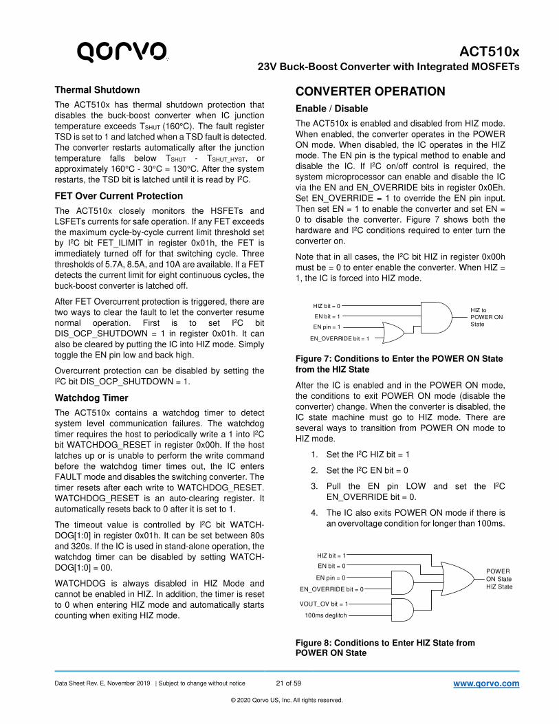
CONVERTER OPERATION
Enable / Disable
The ACT510x is enabled and disabled from HIZ mode.
When enabled, the converter operates in the POWER
ON mode. When disabled, the IC operates in the HIZ
mode. The EN pin is the typical method to enable and
disable the IC. If I2C on/off control is required, the
system microprocessor can enable and disable the IC
via the EN and EN_OVERRIDE bits in register 0x0Eh.
Set EN_OVERRIDE = 1 to override the EN pin input.
Then set EN = 1 to enable the converter and set EN =
0 to disable the converter. Figure 7 shows both the
hardware and I2C conditions required to enter turn the
converter on.
Note that in all cases, the I2C bit HIZ in register 0x00h
must be = 0 to enter enable the converter. When HIZ =
1, the IC is forced into HIZ mode.
HIZ bit = 0
EN bit = 1
EN pin = 1
EN_OVERRIDE bit = 1
HIZ to
POWER ON
State
Figure 7: Conditions to Enter the POWER ON State
from the HIZ State
After the IC is enabled and in the POWER ON mode,
the conditions to exit POWER ON mode (disable the
converter) change. When the converter is disabled, the
IC state machine must go to HIZ mode. There are
several ways to transition from POWER ON mode to
HIZ mode.
1. Set the I2C HIZ bit = 1
2. Set the I2C EN bit = 0
3. Pull the EN pin LOW and set the I2C
EN_OVERRIDE bit = 0.
4. The IC also exits POWER ON mode if there is
an overvoltage condition for longer than 100ms.
HIZ bit = 1
EN bit = 0
EN pin = 0
EN_OVERRIDE bit = 0
POWER
ON State to
HIZ State
VOUT_OV bit = 1
100ms deglitch
Figure 8: Conditions to Enter HIZ State from POWER ON State
Data Sheet Rev. E, November 2019 | Subject to change without notice 22 of 59 www.qorvo.com
© 2020 Qorvo US, Inc. All rights reserved.
ACT510x
23V Buck-Boost Converter with Integrated MOSFETs
Output Voltage Setting
The output voltage is programmable between 2.96V
and 23.42V in 20mV steps via by I2C bits VOUT[9:0] in
registers 0x13h and 0x14h.
= 2.96 + 20 ∗ [9: 0] Where VOUT[9:0] is the decimal equivalent of the value
in this register. For example, if VOUT[9:0] =
0111000100b (452 decimal), the output voltage = 2.96V
+ 0.02V * 452 = 12.00V.
When changing from one output voltage to another, the
slew rate is programmable between 1V/ms and 0.1V/ms
by I2C bits OUTPUT_SLEW[1:0] in register 0x10h. This
allows the output to conform to QC2.0/QC3.0/USB PD/
USB PD + PPS functions for higher output voltages.
The input voltage must always stay above the minimum
allowable input voltage. This voltage is defined by reg-
isters VIN_UV_OFFSET in register 0x1Ah and VIN_UV
in register 0x0Fh. The minimum allowable input voltage
is the VIN_UV_OFFSET voltage minus the VIN_UV
voltage. If the input voltage drops below this value, the
IC turns off the output and goes to the RST state.
Active Discharge
When changing the output voltage to a higher level, the
switcher ramps the output voltage by the programmed
slew rate. When the output voltage is programmed from
a higher to a lower voltage, the voltage drops at a rate
determined by the output capacitance and the load
current. To minimize the fall time in no-load conditions,
the ACT510x can provide a 70mA sink when the output
is transitioning to a lower output voltage. Enable this
feature by writing 1 into I2C bit PULLDOWN_RAMP.
The 70mA load turns on until the output voltage goes
into regulation.
Enable Delay
Once the IC has the valid conditions for startup, the
Enable Delay timer is enabled. The timer options allow
a 0ms to 1s delay. The startup delay is controlled by the
I2C bits EN_DLY[1:0]
Soft Start
After the Enable Delay has completed, the IC starts the
output using a soft start function programmable by the
I2C bits SOFT_START in register 0x0Eh. The softstart
time is independent of the output voltage setting.
Setting Maximum Output Current
The maximum output current, IOUT_MAX, is set by a
combination of a current sense resistor, an OLIM
resistor, and a scaling factor defined by I2C bits CC[6:0]
in register 0x17h. The maximum allowable output
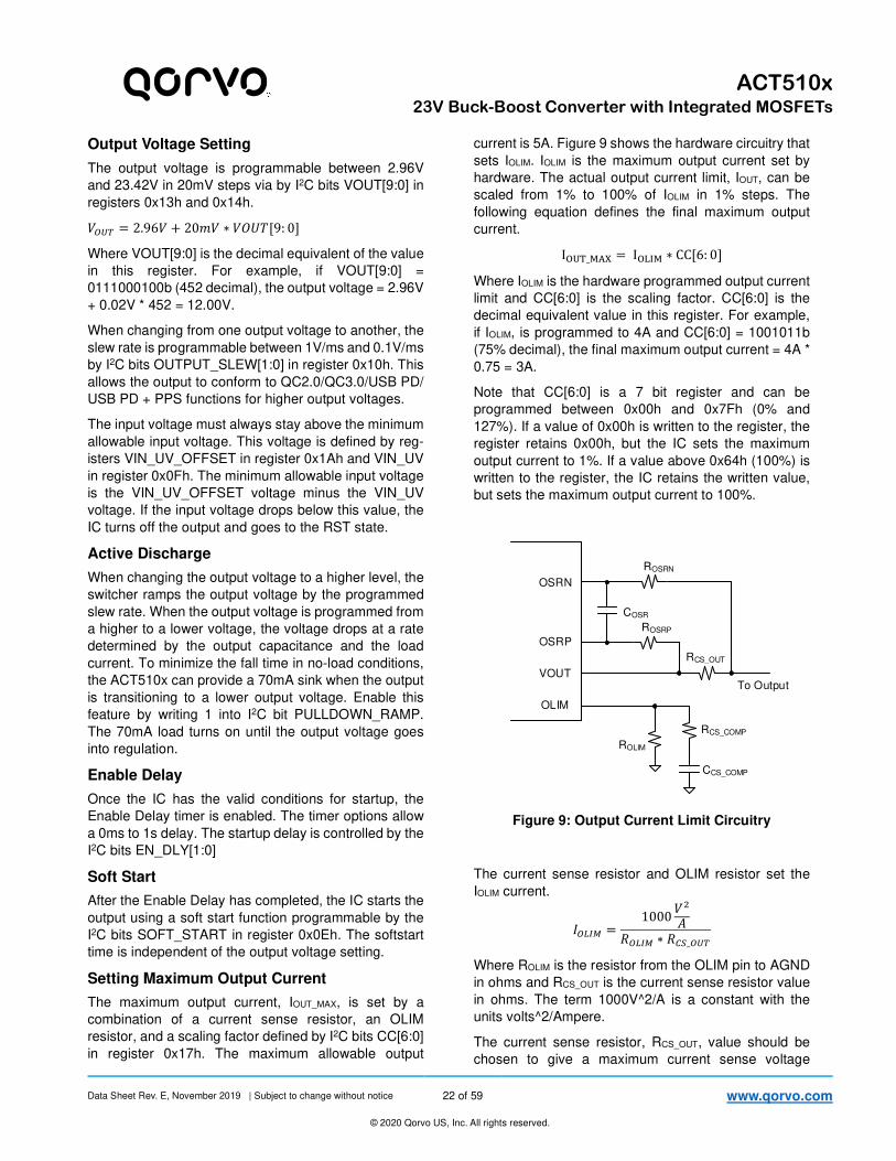
current is 5A. Figure 9 shows the hardware circuitry that
sets IOLIM. IOLIM is the maximum output current set by
hardware. The actual output current limit, IOUT, can be
scaled from 1% to 100% of IOLIM in 1% steps. The
following equation defines the final maximum output
current.
I_ = I ∗ CC[6: 0] Where IOLIM is the hardware programmed output current
limit and CC[6:0] is the scaling factor. CC[6:0] is the
decimal equivalent value in this register. For example,
if IOLIM, is programmed to 4A and CC[6:0] = 1001011b
(75% decimal), the final maximum output current = 4A *
0.75 = 3A.
Note that CC[6:0] is a 7 bit register and can be
programmed between 0x00h and 0x7Fh (0% and
127%). If a value of 0x00h is written to the register, the
register retains 0x00h, but the IC sets the maximum
output current to 1%. If a value above 0x64h (100%) is
written to the register, the IC retains the written value,
but sets the maximum output current to 100%.
To Output
RCS_OUT
ROLIM
ROSRN
ROSRP
COSR
OSRN
OSRP
VOUT
OLIM
RCS_COMP
CCS_COMP
Figure 9: Output Current Limit Circuitry
The current sense resistor and OLIM resistor set the
IOLIM current.
!"# = 1000 %&
'!"# ∗ '()_
Where ROLIM is the resistor from the OLIM pin to AGND
in ohms and RCS_OUT is the current sense resistor value
in ohms. The term 1000V^2/A is a constant with the
units volts^2/Ampere.
The current sense resistor, RCS_OUT, value should be
chosen to give a maximum current sense voltage

Data Sheet Rev. E, November 2019 | Subject to change without notice 23 of 59 www.qorvo.com
© 2020 Qorvo US, Inc. All rights reserved.
ACT510x
23V Buck-Boost Converter with Integrated MOSFETs
between 20mV and 50mV. 50mV is the absolute
maximum allowable voltage. Using lower voltages
reduces the resistor’s power dissipation, but decreases
accuracy. At lower output currents, additional RC
compensation must be placed in parallel with ROLIM. Ta-
ble 4 gives recommended resistor values for different
values of IOLIM current. Contact [email protected]
for compensation information if other configurations are
required.
Table 4: Output Current Component Selection
Switching Frequency = 125kHz
IOLIM (A) RCS
(mΩ)
ROLIM
(kΩ)
RCS_COMP
(kΩ)
CCS_COMP
(nF)
5 10 20 NA NA
4 10 25 NA NA
3 10 33 10 330 2 10 50 10 330
1.5 20 33 10 330
1 20 50 10 330
Switching Frequency = 250kHz, 500kHz, 1MHz
IOLIM (A) RCS
(mΩ) ROLIM
(kΩ) RCS_COMP
(kΩ)
CCS_COMP
(nF) 5 10 20 NA NA
4 10 25 NA NA
3 10 33 NA NA
2 10 50 15 56
1.5 20 33 10 100 1 20 50 10 100
To eliminate noise in the current measurement circuit,
the current sense voltage must be filtered. The
recommended values are ROSRP = ROSRN = 30.1ohm and
COSR = 100nF. These values can be scaled up or down,
but ROSRP must be between 20ohm and 50ohm, and the
resulting filter cutoff frequency must be between 20kHz
and 30kHz.
The actual output current can be measured with the
OLIM pin. The OLIM voltage is directly proportional to
the output current. The following equation calculates the
actual output current.
= !"#!"#
2
Where IOLIM is the hardware programmed 100% output
current limit in amps and VOLIM is the voltage measured
at the OLIM pin.
Constant Output Current Regulation
When the output current tries to increase above IOUT_MAX,
the converter transitions from constant output voltage
regulation to constant output current regulation. The
output voltage will drop to maintain a constant output
current.
I2C bit OUTPUT_CC in register 0x20h indicates if the
converter is operating in constant voltage or current
regulation. When this bit = 0, the IC is regulating in
constant voltage mode. When this bit = 1, the IC is
regulating in constant current mode. If the output drops
below 3V, the IC assumes an output fault has occurred
and disables the output for 3s. This is the HICCUP state.
After 3s, the state machine goes to RST and restarts. If
a short or high current fault is present after the restart,
the IC cycles back to HICCUP and RST. This cycle
continues indefinitely until the converter is disabled or
the fault is removed.
Input Current Regulation
At all times during operation, the IC monitors the current
across the input current sense resistor (ISRP and ISRN)
to provide input current protection. This provides
compatibility with USB input current limitations and
avoids over loading weak input voltage sources.
Figure 10 shows that the input current limiting circuitry
is identical to the output current setting circuitry. When
the input current reaches current limit, the ACT510x
control circuitry starts regulating the maximum input
current. This can cause the output voltage to drop if the
load resistance continues to decrease. The maximum
allowable input current is 5A. The actual input current
limit, IIN_LIM can be scaled to 150% or 200% of IILIM. The
following equation defines the final input current limit.
"*_!"# = "!"# ∗ +,_ - .[1: 0] Where IILIM is the hardware programmed current limit
and INPUT_ILIM[1:0] is the scaling factor. INPUT_ILIM
can be 150% or 200% of IILIM. When INPUT_ILIM is
programmed to 00, input current limiting is disabled.
From Input
Supply
RCS_IN
RILIM
RISRP
RISRN
CISR
ISRP
ISRN
VIN
ILIM
RCS_COMP
CCS_COMP
Figure 10: Input Current Circuitry
Data Sheet Rev. E, November 2019 | Subject to change without notice 24 of 59 www.qorvo.com
© 2020 Qorvo US, Inc. All rights reserved.
ACT510x
23V Buck-Boost Converter with Integrated MOSFETs
The current sense resistor and ILIM resistor set the IILIM
current.
"!"# = 1000 %&
'"!"# ∗ '()_"*
Where RILIM is the resistor from the ILIM pin to AGND
and RCS_IN is the current sense resistor value in ohms.
The term 1000V^2/A is a constant with the units
volts^2/Ampere.
The current sense resistor, RCS_IN, has the same
limitations as RCS_OUT. At lower maximum input currents,
additional RC compensation must be placed in parallel
with RILIM. Table 4 is also valid for the input current limit
circuitry.
The input current limit circuitry, RISRP = RISRN = 30.1ohm
and CISR also have the same input filter requirements as
the output current circuitry.
The actual input current can also be externally
measured with the ILIM pin. The ILIM voltage is directly
proportional to the input current. The following equation
calculates the actual input current.
"* = "!"#"!"#
2
Table 5: I2C Input Current Limit Setting
INPUT_ILIM[1:0] Register Setting
Input Current Scaling Factor
00 Disabled
01 150% of IILIM
10 200% of IILIM
11 150% of IILIM
VOUT Over-Voltage Protection
To detect a possible plug in of a higher voltage supply
on VOUT, the IC detects an overvoltage condition on
VOUT and immediately stops switching. The output
overvoltage threshold is fixed at 108% of the
programmed output voltage. If the OV condition lasts for
more than 100ms, the IC exits POWER ON Mode and
enters HIZ Mode.
Cord Compensation
ACT510x provides cord compensation at the output.
This feature compensates for system level voltage
drops due to PCB, connector, and wiring resistances.
These resistances reduce the output voltage at the load.
The ACT510x features Cord Compensation which
allows the user to compensate for these system level
resistances by increasing the voltage regulation set
point proportional to the output current. The output
voltage increases linearly with increasing load current.
The I2C CORD_COMP[1:0] bits in register 0x0F set the
Cord Comp value.
The Cord Compensation value is normalized to RCS_OUT
= 10mΩ and a 2.4A load current. It scales linearly with
changes in current sense resistance or load current.
(/01_(/23 = (45_(#6 ∗ 2.4& ∗ '()_
0.01Ω
Where VCORD_COMP is the I2C Cord Compensation value
of 100mV, 200mV, or 300mV per Table 6, IOUT is the
actual output current in Amperes, and RCS_OUT is the
current sense value in Ohms.
Table 6: Cord Comp Setting
CORD_COMP[1:0] Setting
Cord Comp Value
Equivalent System
Resistance
00 0 (Disabled) 0mΩ
01 100mV 41.7mΩ
10 200mV 83.3mΩ
11 300mV 125.0mΩ
Light Load Disable
The ACT510x includes a Light Load Disable function.
This function maximizes battery life when the IC is
powered from a battery. It turns off the output and puts
the IC into HIZ mode when the load drops very low. This
condition typically happens when the ACT510x output
supplies power to a charging portable device. When the
portable device is fully charged, the output current drops
to 0A. Light Load Disable minimizes battery current (the
input to the ACT510x) consumption and extends battery
life when the output is not needed.
Light Load Disable is available when the IC is operating
in buck mode, VIN is higher than VOUT by a minimum
of 0.5V, and the Output Voltage is less than 6V. Enable
Light Load Disable by setting I2C bit OFF_LOAD_EN in
register 0x0Eh = 1. Setting this bit = 0 disables the
feature. The minimum current is set to 5mA typical. The
current must be low for longer than the time set in I2C
bit OFF_DLY[1:0]. This time can programmed to 10s,
20s, or 30s.
Once the state machine has detected a light load con-
dition, it enters the LL_DIS state. The IC must exit
POWER ON mode and re-enter POWER ON mode to
restart the converter. This is typically accomplished by
toggling the EN pin, but can also be accomplished via
I2C.
Data Sheet Rev. E, November 2019 | Subject to change without notice 25 of 59 www.qorvo.com
© 2020 Qorvo US, Inc. All rights reserved.
ACT510x
23V Buck-Boost Converter with Integrated MOSFETs
Output Voltage DVS (ACT5101 only)
The ACT5101 is ideally suited for many industry stand-
ard charging protocols such as USB PD3.0, QC2.0,
QC3.0, etc. This includes USB PD3.0 + PPD. To
achieve this compatibility, the output voltage can be dy-
namically changed. VOUT in can be dynamically
changed by writing to the VOUT[10:0] register. The
OUTPUT_SLEW[1:0] register controls the slew rate be-
tween settings when the VOUT[10:0] is changed. When
the voltage is increased, the internal ramp and regulator
can compensate and increase the voltage. However,
when the voltage is decreased, and there is no external
load on the output, the output voltage may not decrease
fast enough to the meet the requirements. To speed up
the transition time from higher to lower output voltages,
set PULLDOWN_RAMP=1. This turns on an internal
70mA load when the output voltage is stepped to a
lower voltage using the VOUT[10:0] register. The 70mA
load turns off when the voltage goes into regulation.
The ACT5101 also has a pulldown current that goes ac-
tive during any output overvoltage condition. Enable this
feature by setting the I2C bit PULLDOWN_OV = 1.
POWER ON State Machine Status
The I2C bits STATUS[2:0] in register 0x20h provide the
user with real time status of the POWER ON state ma-
chine. These bits are always 000 when the IC is not in
POWER ON mode.
Table 7: POWER ON State Machine Status
STATUS[2:0] State Machine State
000 RST
001 SS
010 REG
011 HICCUP
100 LL_DIS
101-111 Not Valid
Frequency
The ACT510x can operate at 125kHz, 250kHz, 500kHz,
or 1MHz. The switching frequency is set by the factory
and is not user programmable. The default frequency is
500kHz to give the best tradeoff between size and
efficiency, but can be programmed to the other options
with a custom CMI. Note that the external component
value requirements change with different switching
frequencies. Contact [email protected] for
additional information about other configurations.
Input Capacitor Selection
The input is connected directly to the VIN pins. The
capacitor should be dedicated high quality, low-ESR,
ceramic capacitor that is optimally placed to minimize
the power routing. 22uF to 47uF capacitors are typically
acceptable, but the final value is application dependent.
Choose the input capacitor value to keep the input
voltage ripple less than ~50mV. The CIN input capacitor
can be increased without limit.
C9 = I ∗:;<=
:>? ∗@AB:;<=:>? C
DEF∗GHIJJKL
Where CIN is the input capacitance in uF, IOUT is the
output current in Amperes, VOUT is the output voltage in
volts, VIN is the input voltage in volts, FSW is the
switching frequency in Hz, and Vripple is the maximum
allowable input voltage ripple in volts.
If the input source is a battery, no additional capacitance
is needed. If the input source is a power supply rail,
adding an additional 100uF bulk electrolytic capacitor is
recommended.
The ceramic capacitor PCB placement is critical. Refer
to the Layout Guidelines selection and to the EVK layout
for details.
Be sure to consider the input capacitor’s DC bias effects.
A capacitor’s actual capacitance is strongly affected by
its DC bias characteristics. The input capacitor is typi-
cally an X5R, X7R, or similar dielectric. Use of Y5U, Z5U,
or similar dielectrics is not recommended. Input
capacitor placement is critical for proper operation. The
input capacitor must be placed as close to the IC as
possible. The traces from VBAT to the capacitor and
from the capacitor to PGND should as short and wide
as possible.
Output Capacitor Selection
The output capacitors are connected directly to VOUT.
The output capacitance must be a combination of
ceramic and bulk capacitance.
Table 8 gives the required capacitor values for stability.
Note that the table has two output capacitor options:
Standard Capacitance and Minimum Capacitance. The
Standard Capacitance design requires more overall
capacitance, but places no restriction on the bulk
capacitor ESR. The Minimum Capacitance design
results in an overall smaller design, but places
restrictions on the ESR. The capacitor values can be
increased without limit.
Note that the Ceramic and Bulk capacitor values are
recommended “Capacitor Values”. When choosing the
ceramic capacitors, use X5R or X7R dielectrics and be
Data Sheet Rev. E, November 2019 | Subject to change without notice 26 of 59 www.qorvo.com
© 2020 Qorvo US, Inc. All rights reserved.
ACT510x
23V Buck-Boost Converter with Integrated MOSFETs
sure to consider the capacitor’s tolerance and DC bias
effects. Use of Y5U, Z5U, or similar dielectrics is not
recommended. The 22uF capacitor must have at least
9uF of effective capacitance for stability. The 47uF
capacitor must have 19uF of capacitance. The bulk
capacitors do not have DC bias effects.
Output ceramic capacitor placement is critical for proper
operation. The output capacitor must be placed as close
to the IC as possible. The traces from VOUT to the
capacitor and from the capacitor to PGND should as
short and wide as possible. The bulk capacitor should
be placed to the right of the current sense resistor. Refer
to the Layout Guidelines selection and to the EVK layout
for additional details.
Inductor Selection
The buck-boost regulator utilizes current-mode control
and a proprietary compensation scheme to simultane-
ously compensate the buck, buck-boost, and boost
modes of operation. The ACT510x compensation
requires a fixed inductor value that is matched to the
switching frequency. Table 8 gives the required inductor
value. Choose an inductor with a low DC-resistance,
and avoid inductor saturation by choosing inductors with
DC ratings that exceed the maximum output current by
at least 30%. The inductor value must be within +30%
to -30% across all operating conditions.
Compensation
The ACT510x operates in three switching modes: buck,
buck-boost, and boost mode depending on the input
and output voltage ratios. The IC contains a proprietary
compensation scheme to simultaneously compensate
all three switching modes. The compensation values
are directly tied to the switching frequency and required
inductor value. Table 8 provides the required compen-
sation values when the IC can operate in all three
switching modes Table 9 provides optimized
compensation values when the IC will only be operating
in Buck mode. Figure 11 shows the compensation
components
Be sure to consider the input capacitor’s DC bias effects.
A capacitor’s actual capacitance is strongly affected by
its DC bias characteristics. The input capacitor is
typically an X5R, X7R, or similar dielectric. Use of Y5U,
Z5U, or similar dielectrics is not recommended.
Input capacitor placement is critical for proper operation.
The input ceramic capacitor must be placed as close to
the IC as possible. The traces from VIN to the capacitor
and from the capacitor to PGND should as short and
wide as possible. Refer to the Layout Guidelines
selection and to the EVK layout for details.
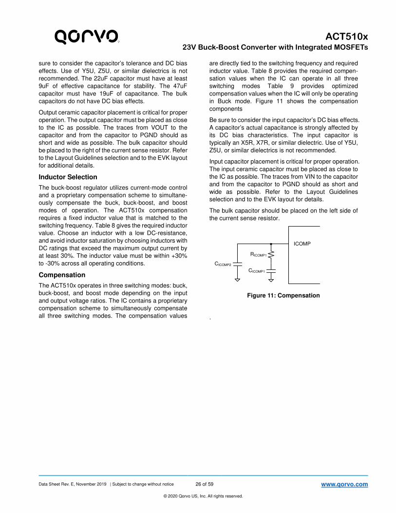
The bulk capacitor should be placed on the left side of
the current sense resistor.
ICOMP
RICOMP1
CICOMP1
CICOMP2
Figure 11: Compensation
.
Data Sheet Rev. E, November 2019 | Subject to change without notice 27 of 59 www.qorvo.com
© 2020 Qorvo US, Inc. All rights reserved.
ACT510x
23V Buck-Boost Converter with Integrated MOSFETs
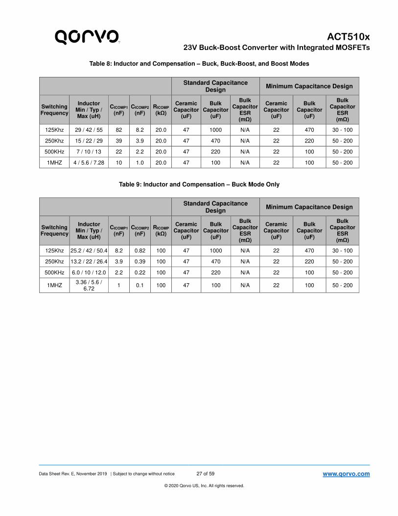
Table 8: Inductor and Compensation – Buck, Buck-Boost, and Boost Modes
Table 9: Inductor and Compensation – Buck Mode Only
Standard Capacitance
Design Minimum Capacitance Design
Switching Frequency
Inductor Min / Typ / Max (uH)
CICOMP1
(nF) CICOMP2
(nF) RICOMP
(kΩ)
Ceramic Capacitor
(uF)
Bulk Capacitor
(uF)
Bulk Capacitor
ESR (mΩ)
Ceramic Capacitor
(uF)
Bulk Capacitor
(uF)
Bulk Capacitor
ESR (mΩ)
125Khz 29 / 42 / 55 82 8.2 20.0 47 1000 N/A 22 470 30 - 100
250Khz 15 / 22 / 29 39 3.9 20.0 47 470 N/A 22 220 50 - 200
500KHz 7 / 10 / 13 22 2.2 20.0 47 220 N/A 22 100 50 - 200
1MHZ 4 / 5.6 / 7.28 10 1.0 20.0 47 100 N/A 22 100 50 - 200
Standard Capacitance
Design Minimum Capacitance Design
Switching Frequency
Inductor Min / Typ / Max (uH)
CICOMP1
(nF) CICOMP2
(nF) RICOMP
(kΩ)
Ceramic Capacitor
(uF)
Bulk Capacitor
(uF)
Bulk Capacitor
ESR (mΩ)
Ceramic Capacitor
(uF)
Bulk Capacitor
(uF)
Bulk Capacitor
ESR (mΩ)
125Khz 25.2 / 42 / 50.4 8.2 0.82 100 47 1000 N/A 22 470 30 - 100
250Khz 13.2 / 22 / 26.4 3.9 0.39 100 47 470 N/A 22 220 50 - 200
500KHz 6.0 / 10 / 12.0 2.2 0.22 100 47 220 N/A 22 100 50 - 200
1MHZ 3.36 / 5.6 /
6.72 1 0.1 100 47 100 N/A 22 100 50 - 200
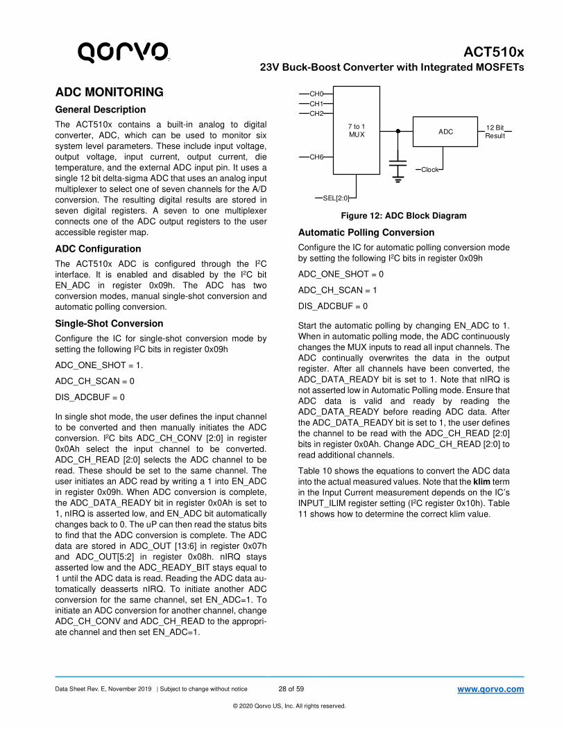
Data Sheet Rev. E, November 2019 | Subject to change without notice 28 of 59 www.qorvo.com
© 2020 Qorvo US, Inc. All rights reserved.
ACT510x
23V Buck-Boost Converter with Integrated MOSFETs
ADC MONITORING
General Description
The ACT510x contains a built-in analog to digital
converter, ADC, which can be used to monitor six
system level parameters. These include input voltage,
output voltage, input current, output current, die
temperature, and the external ADC input pin. It uses a
single 12 bit delta-sigma ADC that uses an analog input
multiplexer to select one of seven channels for the A/D
conversion. The resulting digital results are stored in
seven digital registers. A seven to one multiplexer
connects one of the ADC output registers to the user
accessible register map.
ADC Configuration
The ACT510x ADC is configured through the I2C
interface. It is enabled and disabled by the I2C bit
EN_ADC in register 0x09h. The ADC has two
conversion modes, manual single-shot conversion and
automatic polling conversion.
Single-Shot Conversion
Configure the IC for single-shot conversion mode by
setting the following I2C bits in register 0x09h
ADC_ONE_SHOT = 1.
ADC_CH_SCAN = 0
DIS_ADCBUF = 0
In single shot mode, the user defines the input channel
to be converted and then manually initiates the ADC
conversion. I2C bits ADC_CH_CONV [2:0] in register
0x0Ah select the input channel to be converted.
ADC_CH_READ [2:0] selects the ADC channel to be
read. These should be set to the same channel. The
user initiates an ADC read by writing a 1 into EN_ADC
in register 0x09h. When ADC conversion is complete,
the ADC_DATA_READY bit in register 0x0Ah is set to
1, nIRQ is asserted low, and EN_ADC bit automatically
changes back to 0. The uP can then read the status bits
to find that the ADC conversion is complete. The ADC
data are stored in ADC_OUT [13:6] in register 0x07h
and ADC_OUT[5:2] in register 0x08h. nIRQ stays
asserted low and the ADC_READY_BIT stays equal to
1 until the ADC data is read. Reading the ADC data au-
tomatically deasserts nIRQ. To initiate another ADC
conversion for the same channel, set EN_ADC=1. To
initiate an ADC conversion for another channel, change
ADC_CH_CONV and ADC_CH_READ to the appropri-
ate channel and then set EN_ADC=1.
7 to 1MUX ADC
CH0
CH1
CH6
CH2
12 Bit Result
Clock
SEL[2:0]
Figure 12: ADC Block Diagram
Automatic Polling Conversion
Configure the IC for automatic polling conversion mode
by setting the following I2C bits in register 0x09h
ADC_ONE_SHOT = 0
ADC_CH_SCAN = 1
DIS_ADCBUF = 0
Start the automatic polling by changing EN_ADC to 1.
When in automatic polling mode, the ADC continuously
changes the MUX inputs to read all input channels. The
ADC continually overwrites the data in the output
register. After all channels have been converted, the
ADC_DATA_READY bit is set to 1. Note that nIRQ is
not asserted low in Automatic Polling mode. Ensure that
ADC data is valid and ready by reading the
ADC_DATA_READY before reading ADC data. After
the ADC_DATA_READY bit is set to 1, the user defines
the channel to be read with the ADC_CH_READ [2:0]
bits in register 0x0Ah. Change ADC_CH_READ [2:0] to
read additional channels.
Table 10 shows the equations to convert the ADC data
into the actual measured values. Note that the klim term
in the Input Current measurement depends on the IC’s
INPUT_ILIM register setting (I2C register 0x10h). Table
11 shows how to determine the correct klim value.
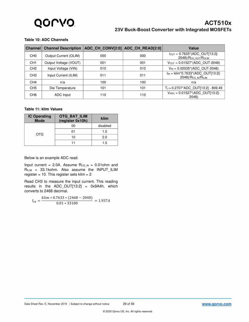
Data Sheet Rev. E, November 2019 | Subject to change without notice 29 of 59 www.qorvo.com
© 2020 Qorvo US, Inc. All rights reserved.
ACT510x
23V Buck-Boost Converter with Integrated MOSFETs
Table 10: ADC Channels
Channel Channel Description ADC_CH_CONV[2:0] ADC_CH_READ[2:0] Value
CH0 Output Current (OLIM) 000 000 IOUT = 0.7633*(ADC_OUT[13:2]-
2048)/RCS_OUT/ROLIM
CH1 Output Voltage (VOUT) 001 001 VOUT = 0.01527*(ADC_OUT-2048)
CH2 Input Voltage (VIN) 010 010 VIN = 0.02035*(ADC_OUT-2048)
CH3 Input Current (ILIM) 011 011 IIN = klim*0.7633*(ADC_OUT[13:2]-
2048)/RCS_IN/RILIM
CH4 n/a 100 100 n/a
CH5 Die Temperature 101 101 TJ = 0.2707*ADC_OUT[13:2] - 809.49
CH6 ADC Input 110 110 VADC = 0.01527*(ADC_OUT[13:2]-
2048)
Table 11: klim Values
IC Operating Mode
OTG_BAT_ILIM (register 0x10h)
klim
OTG
00 disabled
01 1.5
10 2.0
11 1.5
Below is an example ADC read.
Input current = 2.0A. Assume RCS_IN = 0.01ohm and
RILIM = 33.1kohm. Also assume the INPUT_ILIM
register = 10. This register sets klim = 2
Read CH3 to measure the input current. This reading
results in the ADC_OUT[13:2] = 0x9A4h, which
converts to 2468 decimal.
"* = MNO ∗ 0.7633 ∗ (2468 − 2048)0.01 ∗ 33100 = 1.937&
Data Sheet Rev. E, November 2019 | Subject to change without notice 30 of 59 www.qorvo.com
© 2020 Qorvo US, Inc. All rights reserved.
ACT510x
23V Buck-Boost Converter with Integrated MOSFETs
PC BOARD LAYOUT GUIDANCE
Proper parts placement and PCB layout are critical to
the operation of switching power supplies. Follow the
following layout guidelines when designing the
ACT510x PCB. Refer to the Active-Semi ACT510x
Evaluation Kit for layout guidance.
1. Place the ceramic input and output capacitors
as close as possible to the IC. Connect the
input capacitors directly between VIN and
PGND pins on the top layer. Connect the output
capacitors directly between VOUT and PGND
pins on the top layer. Use 1206 sized capacitors
to allow for proper switch pin routing. Note that
the input and output capacitor placement is
critical. Active-Semi strongly recommends
following the EVK input capacitor and output
capacitor placement and routing. The bulk input
and output capacitor placement is not as critical.
Bulk capacitors should be placed on the
opposite side of the sense resistors from the
ceramic capacitors.
2. Minimize the switch node trace lengths
between the SW1 and SW2 pins and the
inductor. Optimal switch node routing is to run
the traces between the input and output
capacitors’ pads. Using 1206 or larger sized
capacitors is recommended. Avoid routing
sensitive analog signals near these high
frequency, high dV/dt traces. Active-Semi
strongly recommends following the EVK
inductor placement and PCB routing.
3. The VINS pin should be Kelvin connected to the
input capacitors. Keep this trace away from the
SW1 and SW2 traces to prevent noise injection.
The IC uses this pin to measure the input
voltage.
4. The PGND and AGND ground pins must be
electrically connected together. The AGND
ground plane should be isolated from the rest
of the PCB power ground. These two ground
pins should be connected together right at the
IC.
5. Connect the exposed pad directly to the top
layer PGND pins and ground plane. Connect
the top layer ground plane to both internal
ground planes and the PCB backside ground
plane with thermal vias. Provide ground plane
routing on multiple layers to allow the IC’s heat
to flow into the PCB and then spread radially
from the IC. Avoid cutting the ground planes or
adding vias that restrict the radial flow of heat.
6. Make Kelvin connections to the ILIM and OLIM
current sense resistors. Route the current
sense signals close to each other and keep
them away from noisy switching signals.
7. The current sense filter capacitors and
inductors should be placed directly by their
respective ISRP, ISRN, OSRP, and OSRN pins.
8. Remember that all open drain outputs need
pull-up resistors.
9. The following components should be
connected to the AGND plane.
ILIM resistor
OLIM resistor
COMP resistor and capacitors
VREG bypass capacitor
INTBP bypass capacitor
10. The ACT510x footprint must connect the VOUT
pins 23, 24, and 35 on the top layer. It must
connect the SW1 pins 21, 22, and 34 on the top
layer. It must connect the SW2 pins 18, 19, and
33 on the top layer.
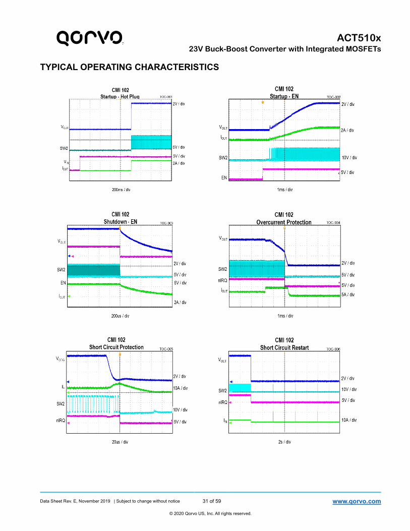
Data Sheet Rev. E, November 2019 | Subject to change without notice 31 of 59 www.qorvo.com
© 2020 Qorvo US, Inc. All rights reserved.
ACT510x
23V Buck-Boost Converter with Integrated MOSFETs
TYPICAL OPERATING CHARACTERISTICS
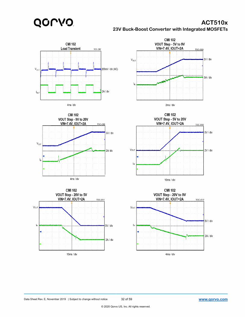
Data Sheet Rev. E, November 2019 | Subject to change without notice 32 of 59 www.qorvo.com
© 2020 Qorvo US, Inc. All rights reserved.
ACT510x
23V Buck-Boost Converter with Integrated MOSFETs
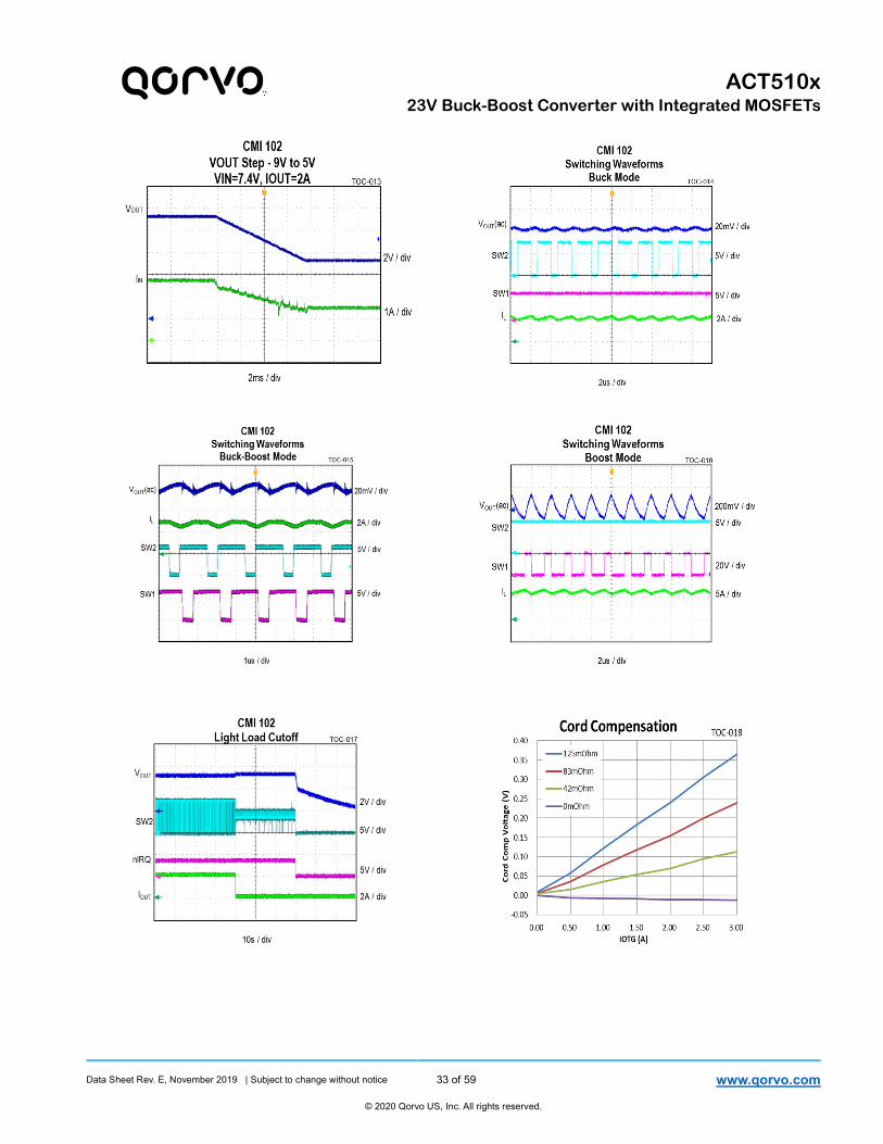
Data Sheet Rev. E, November 2019 | Subject to change without notice 33 of 59 www.qorvo.com
© 2020 Qorvo US, Inc. All rights reserved.
ACT510x
23V Buck-Boost Converter with Integrated MOSFETs
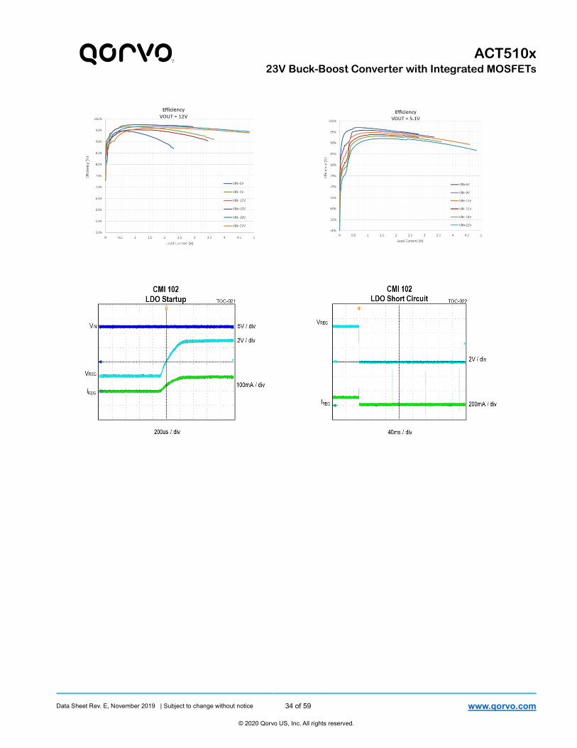
Data Sheet Rev. E, November 2019 | Subject to change without notice 34 of 59 www.qorvo.com
© 2020 Qorvo US, Inc. All rights reserved.
ACT510x
23V Buck-Boost Converter with Integrated MOSFETs
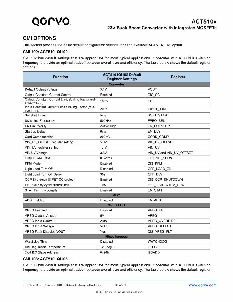
Data Sheet Rev. E, November 2019 | Subject to change without notice 35 of 59 www.qorvo.com
© 2020 Qorvo US, Inc. All rights reserved.
ACT510x
23V Buck-Boost Converter with Integrated MOSFETs
CMI OPTIONS
This section provides the basic default configuration settings for each available ACT510x CMI option.
CMI 102: ACT5101QI102
CMI 102 has default settings that are appropriate for most typical applications. It operates with a 500kHz switching
frequency to provide an optimal tradeoff between overall size and efficiency. The table below shows the default register
settings.
Function ACT5101QI102 Default
Register Settings Register
Converter
Default Output Voltage 5.1V VOUT
Output Constant Current Control Enabled DIS_CC
Output Constant Current Limit Scaling Factor (rel-ative to IOLIM)
100% CC
Input Constant Current Limit Scaling Factor (rela-tive to IILIM)
200% INPUT_ILIM
Softstart Time 5ms SOFT_START
Switching Frequency 500kHz FREQ_SEL
EN Pin Polarity Active High EN_POLARITY
Start up Delay 0ms EN_DLY
Cord Compensation 200mV CORD_COMP
VIN_UV_OFFSET register setting 5.0V VIN_UV_OFFSET
VIN_UV register setting 1.4V VIN_UV
VIN UV Voltage 3.6V VIN_UV and VIN_UV_OFFSET
Output Slew Rate 0.5V/ms OUTPUT_SLEW
PFM Mode Enabled DIS_PFM
Light Load Turn Off Disabled OFF_LOAD_EN
Light Load Turn Off Delay 30s OFF_DLY
OCP Shutdown (8 FET OC cycles) Enabled DIS_OCP_SHUTDOWN
FET cycle by cycle current limit 10A FET_ILIMIT & ILIM_LOW
STAT Pin Functionality Enabled EN_STAT
ADC
ADC Enabled Disabled EN_ADC
VREG LDO
VREG Enabled Enabled VREG_EN
VREG Output Voltage 5V VREG
VREG Input Control Auto VREG_OVERRIDE
VREG Input Voltage VOUT VREG_SELECT
VREG Fault Disables VOUT Yes DIS_VREG_FLT
Miscellaneous
Watchdog Timer Disabled WATCHDOG
Die Regulation Temperature 120 deg C TREG
7-bit I2C Slave Address 0x24h I2CADD
CMI 103: ACT5101QI103
CMI 103 has default settings that are appropriate for most typical applications. It operates with a 500kHz switching
frequency to provide an optimal tradeoff between overall size and efficiency. The table below shows the default register

Data Sheet Rev. E, November 2019 | Subject to change without notice 36 of 59 www.qorvo.com
© 2020 Qorvo US, Inc. All rights reserved.
ACT510x
23V Buck-Boost Converter with Integrated MOSFETs
settings. The difference between ACT5101QI102 and ACT5101QI103 is the 7-bit I2C address. The ACT5101QI103
address changes to 0x66h.
Function ACT5101QI103 Default
Register Settings Register
Converter
Default Output Voltage 5.1V VOUT
Output Constant Current Control Enabled DIS_CC
Output Constant Current Limit Scaling Factor (rel-ative to IOLIM)
100% CC
Input Constant Current Limit Scaling Factor (rela-tive to IILIM)
200% INPUT_ILIM
Softstart Time 5ms SOFT_START
Switching Frequency 500kHz FREQ_SEL
EN Pin Polarity Active High EN_POLARITY
Start up Delay 0ms EN_DLY
Cord Compensation 200mV CORD_COMP
VIN_UV_OFFSET register setting 5.0V VIN_UV_OFFSET
VIN_UV register setting 1.4V VIN_UV
VIN UV Voltage 3.6V VIN_UV and VIN_UV_OFFSET
Output Slew Rate 0.5V/ms OUTPUT_SLEW
PFM Mode Enabled DIS_PFM
Light Load Turn Off Disabled OFF_LOAD_EN
Light Load Turn Off Delay 30s OFF_DLY
OCP Shutdown (8 FET OC cycles) Enabled DIS_OCP_SHUTDOWN
FET cycle by cycle current limit 10A FET_ILIMIT & ILIM_LOW
STAT Pin Functionality Enabled EN_STAT
ADC
ADC Enabled Disabled EN_ADC
VREG LDO
VREG Enabled Enabled VREG_EN
VREG Output Voltage 5V VREG
VREG Input Control Auto VREG_OVERRIDE
VREG Input Voltage VOUT VREG_SELECT
VREG Fault Disables VOUT Yes DIS_VREG_FLT
Miscellaneous
Watchdog Timer Disabled WATCHDOG
Die Regulation Temperature 120 deg C TREG
7-bit I2C Slave Address 0x66h I2CADD
CMI 102: ACT5102QI102
CMI 102 has default settings that are appropriate for most typical applications. It operates with a 500kHz switching
frequency to provide an optimal tradeoff between overall size and efficiency. The table below shows the default register
settings. The difference between the ACT5101QI102 and ACT5102QI102 is that the ACT5102QI102 has external volt-
age feedback and does not have the ADC functionality.
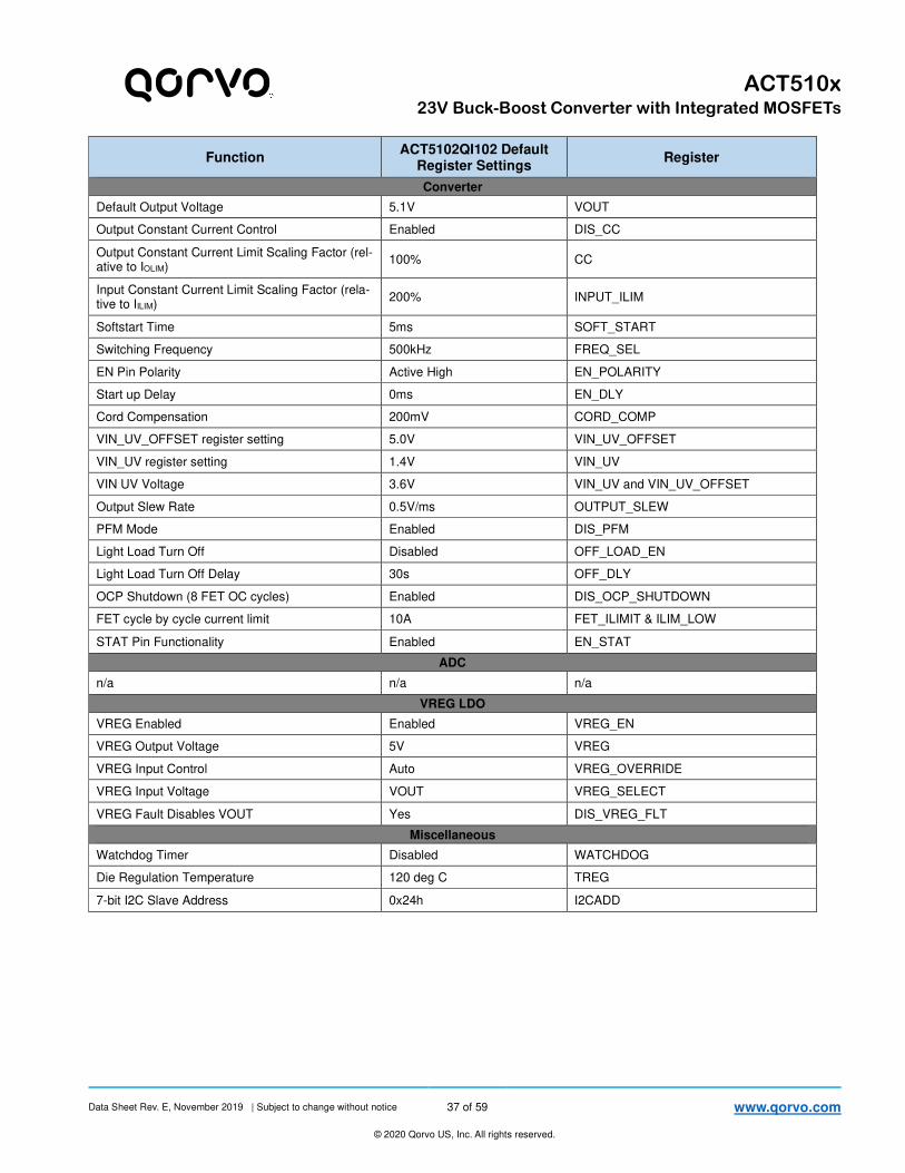
Data Sheet Rev. E, November 2019 | Subject to change without notice 37 of 59 www.qorvo.com
© 2020 Qorvo US, Inc. All rights reserved.
ACT510x
23V Buck-Boost Converter with Integrated MOSFETs
Function ACT5102QI102 Default
Register Settings Register
Converter
Default Output Voltage 5.1V VOUT
Output Constant Current Control Enabled DIS_CC
Output Constant Current Limit Scaling Factor (rel-ative to IOLIM)
100% CC
Input Constant Current Limit Scaling Factor (rela-tive to IILIM)
200% INPUT_ILIM
Softstart Time 5ms SOFT_START
Switching Frequency 500kHz FREQ_SEL
EN Pin Polarity Active High EN_POLARITY
Start up Delay 0ms EN_DLY
Cord Compensation 200mV CORD_COMP
VIN_UV_OFFSET register setting 5.0V VIN_UV_OFFSET
VIN_UV register setting 1.4V VIN_UV
VIN UV Voltage 3.6V VIN_UV and VIN_UV_OFFSET
Output Slew Rate 0.5V/ms OUTPUT_SLEW
PFM Mode Enabled DIS_PFM
Light Load Turn Off Disabled OFF_LOAD_EN
Light Load Turn Off Delay 30s OFF_DLY
OCP Shutdown (8 FET OC cycles) Enabled DIS_OCP_SHUTDOWN
FET cycle by cycle current limit 10A FET_ILIMIT & ILIM_LOW
STAT Pin Functionality Enabled EN_STAT
ADC
n/a n/a n/a
VREG LDO
VREG Enabled Enabled VREG_EN
VREG Output Voltage 5V VREG
VREG Input Control Auto VREG_OVERRIDE
VREG Input Voltage VOUT VREG_SELECT
VREG Fault Disables VOUT Yes DIS_VREG_FLT
Miscellaneous
Watchdog Timer Disabled WATCHDOG
Die Regulation Temperature 120 deg C TREG
7-bit I2C Slave Address 0x24h I2CADD
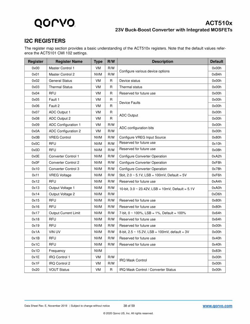
Data Sheet Rev. E, November 2019 | Subject to change without notice 38 of 59 www.qorvo.com
© 2020 Qorvo US, Inc. All rights reserved.
ACT510x
23V Buck-Boost Converter with Integrated MOSFETs
I2C REGISTERS
The register map section provides a basic understanding of the ACT510x registers. Note that the default values refer-
ence the ACT5101 CMI 102 settings.
Register Register Name Type R/W Description Default
0x00 Master Control 1 VM R/W Configure various device options
0x00h
0x01 Master Control 2 NVM R/W 0xB4h
0x02 General Status VM R Device status 0x00h
0x03 Thermal Status VM R Thermal status 0x00h
0x04 RFU VM R Reserved for future use 0x00h
0x05 Fault 1 VM R Device Faults
0x00h
0x06 Fault 2 VM R 0x00h
0x07 ADC Output 1 VM R ADC Output
0x00h
0x08 ADC Output 2 VM R 0x00h
0x09 ADC Configuration 1 VM R/W ADC configuration bits
0x00h
0x0A ADC Configuration 2 VM R/W 0x00h
0x0B VREG Control NVM R/W Configure VREG Input Source 0x80h
0x0C RFU NVM R/W Reserved for future use 0x10h
0x0D RFU NVM R/W Reserved for future use 0x08h
0x0E Converter Control 1 NVM R/W Configure Converter Operation 0xA2h
0x0F Converter Control 2 NVM R/W Configure Converter Operation 0xF8h
0x10 Converter Control 3 NVM R/W Configure Converter Operation 0x78h
0x11 VREG Voltage NVM R/W 5bit, 2.0 ~ 5.1V, LSB = 100mV, Default = 5V 0xF6h
0x12 RFU NVM R/W Reserved for future use 0xA4h
0x13 Output Voltage 1 NVM R/W 10-bit, 3.0 ~ 23.42V, LSB = 10mV, Default = 5.1V
0xA0h
0x14 Output Voltage 2 NVM R/W 0xD6h
0x15 RFU NVM R/W Reserved for future use 0x80h
0x16 RFU NVM R/W Reserved for future use 0x80h
0x17 Output Current Limit NVM R/W 7-bit, 0 ~ 100%, LSB = 1%, Default = 100% 0x64h
0x18 RFU NVM R/W Reserved for future use 0x64h
0x19 RFU NVM R/W Reserved for future use 0x00h
0x1A VIN UV NVM R/W 8-bit, 2.5 ~ 15.2V, LSB = 100mV, default = 3V 0x00h
0x1B RFU NVM R/W Reserved for future use 0x40h
0x1C RFU NVM R/W Reserved for future use 0x40h
0x1D Frequency NVM 0x83h
0x1E IRQ Control 1 VM R/W IRQ Mask Control
0x00h
0x1F IRQ Control 2 VM R/W 0x00h
0x20 VOUT Status VM R IRQ Mask Control / Converter Status 0x00h
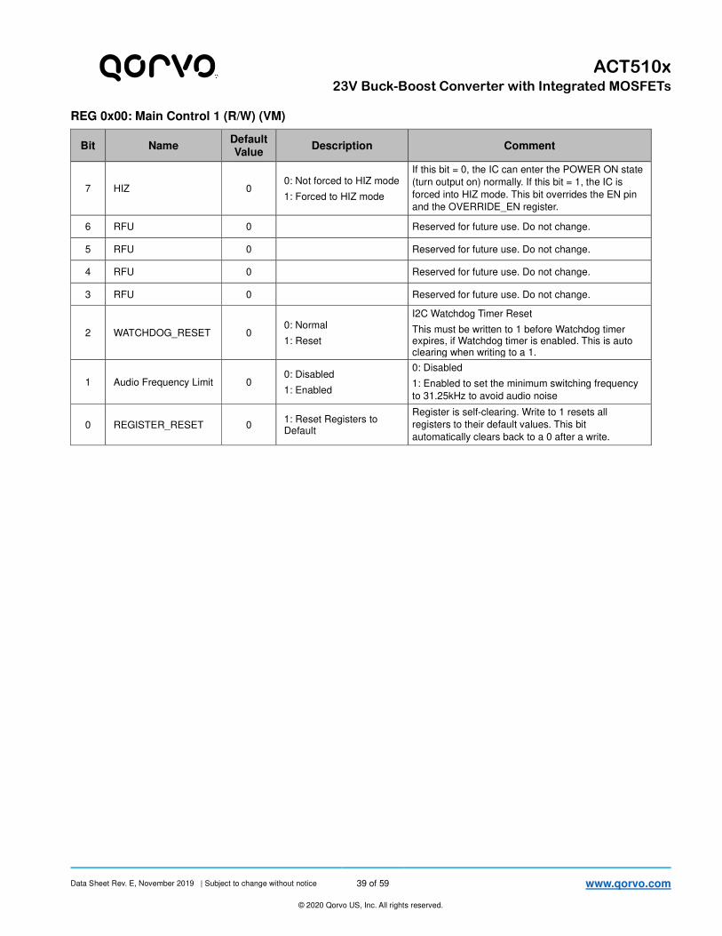
Data Sheet Rev. E, November 2019 | Subject to change without notice 39 of 59 www.qorvo.com
© 2020 Qorvo US, Inc. All rights reserved.
ACT510x
23V Buck-Boost Converter with Integrated MOSFETs
REG 0x00: Main Control 1 (R/W) (VM)
Bit Name Default Value
Description Comment
7 HIZ 0 0: Not forced to HIZ mode
1: Forced to HIZ mode
If this bit = 0, the IC can enter the POWER ON state
(turn output on) normally. If this bit = 1, the IC is
forced into HIZ mode. This bit overrides the EN pin
and the OVERRIDE_EN register.
6 RFU 0 Reserved for future use. Do not change.
5 RFU 0 Reserved for future use. Do not change.
4 RFU 0 Reserved for future use. Do not change.
3 RFU 0 Reserved for future use. Do not change.
2 WATCHDOG_RESET 0 0: Normal
1: Reset
I2C Watchdog Timer Reset
This must be written to 1 before Watchdog timer expires, if Watchdog timer is enabled. This is auto clearing when writing to a 1.
1 Audio Frequency Limit 0 0: Disabled
1: Enabled
0: Disabled
1: Enabled to set the minimum switching frequency
to 31.25kHz to avoid audio noise
0 REGISTER_RESET 0 1: Reset Registers to Default
Register is self-clearing. Write to 1 resets all
registers to their default values. This bit
automatically clears back to a 0 after a write.
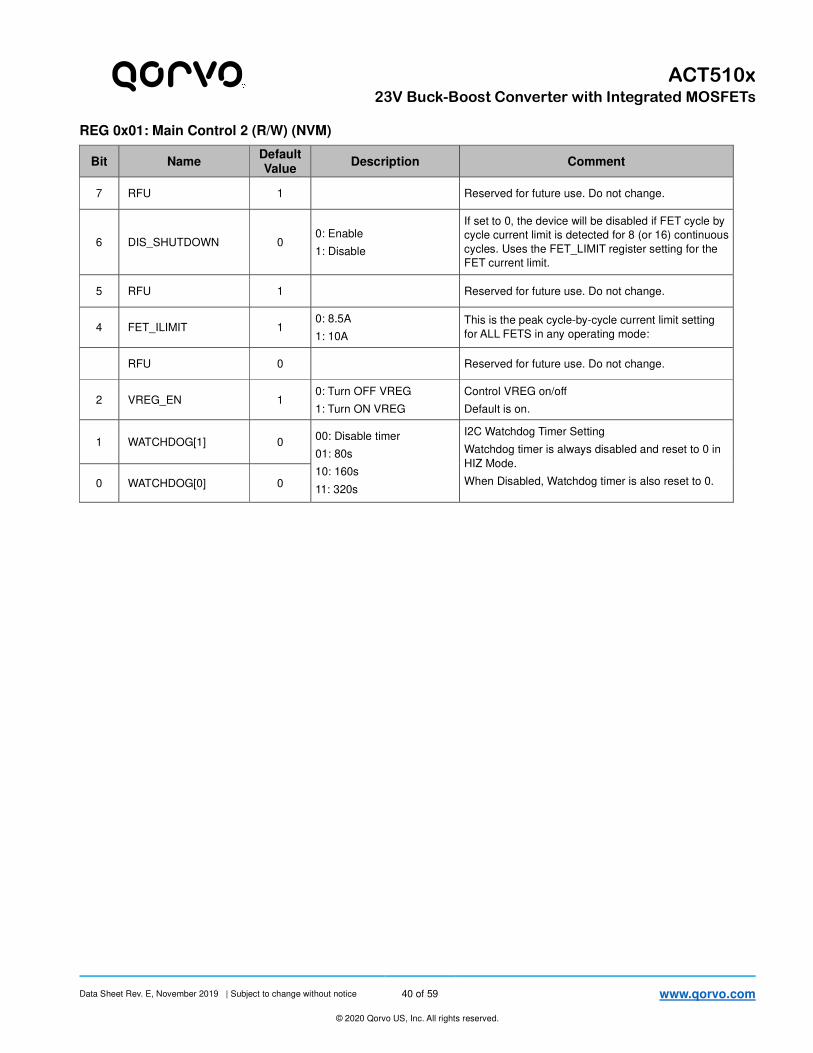
Data Sheet Rev. E, November 2019 | Subject to change without notice 40 of 59 www.qorvo.com
© 2020 Qorvo US, Inc. All rights reserved.
ACT510x
23V Buck-Boost Converter with Integrated MOSFETs
REG 0x01: Main Control 2 (R/W) (NVM)
Bit Name Default Value
Description Comment
7 RFU 1 Reserved for future use. Do not change.
6 DIS_SHUTDOWN 0 0: Enable
1: Disable
If set to 0, the device will be disabled if FET cycle by
cycle current limit is detected for 8 (or 16) continuous
cycles. Uses the FET_LIMIT register setting for the
FET current limit.
5 RFU 1 Reserved for future use. Do not change.
4 FET_ILIMIT 1 0: 8.5A
1: 10A
This is the peak cycle-by-cycle current limit setting
for ALL FETS in any operating mode:
RFU 0 Reserved for future use. Do not change.
2 VREG_EN 1 0: Turn OFF VREG
1: Turn ON VREG
Control VREG on/off
Default is on.
1 WATCHDOG[1] 0 00: Disable timer
01: 80s
10: 160s
11: 320s
I2C Watchdog Timer Setting
Watchdog timer is always disabled and reset to 0 in
HIZ Mode.
When Disabled, Watchdog timer is also reset to 0.
0 WATCHDOG[0] 0
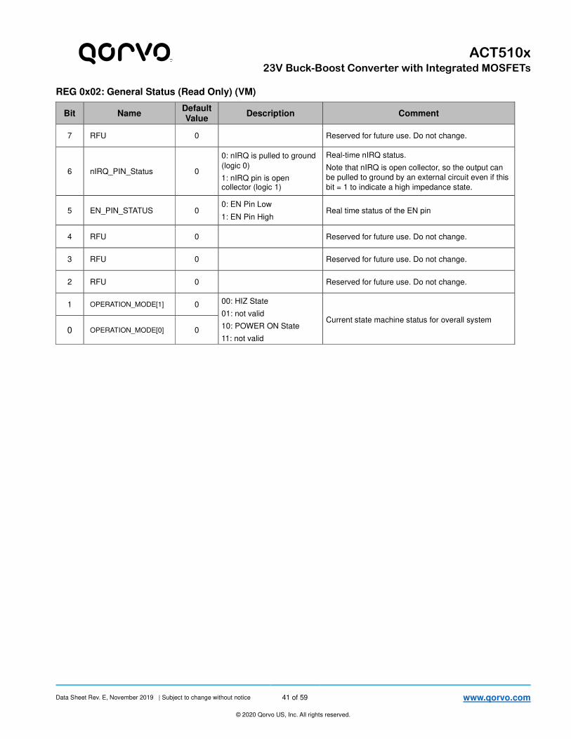
Data Sheet Rev. E, November 2019 | Subject to change without notice 41 of 59 www.qorvo.com
© 2020 Qorvo US, Inc. All rights reserved.
ACT510x
23V Buck-Boost Converter with Integrated MOSFETs
REG 0x02: General Status (Read Only) (VM)
Bit Name Default Value
Description Comment
7 RFU 0 Reserved for future use. Do not change.
6 nIRQ_PIN_Status 0
0: nIRQ is pulled to ground
(logic 0)
1: nIRQ pin is open collector (logic 1)
Real-time nIRQ status.
Note that nIRQ is open collector, so the output can
be pulled to ground by an external circuit even if this
bit = 1 to indicate a high impedance state.
5 EN_PIN_STATUS 0 0: EN Pin Low
1: EN Pin High Real time status of the EN pin
4 RFU 0 Reserved for future use. Do not change.
3 RFU 0 Reserved for future use. Do not change.
2 RFU 0 Reserved for future use. Do not change.
1 OPERATION_MODE[1] 0 00: HIZ State
01: not valid
10: POWER ON State
11: not valid
Current state machine status for overall system
0 OPERATION_MODE[0] 0
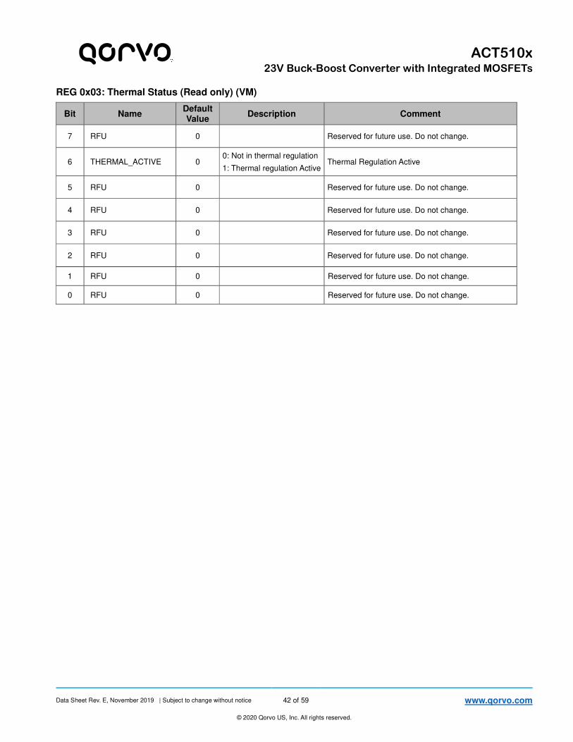
Data Sheet Rev. E, November 2019 | Subject to change without notice 42 of 59 www.qorvo.com
© 2020 Qorvo US, Inc. All rights reserved.
ACT510x
23V Buck-Boost Converter with Integrated MOSFETs
REG 0x03: Thermal Status (Read only) (VM)
Bit Name Default Value
Description Comment
7 RFU 0 Reserved for future use. Do not change.
6 THERMAL_ACTIVE 0 0: Not in thermal regulation
1: Thermal regulation Active Thermal Regulation Active
5 RFU 0 Reserved for future use. Do not change.
4 RFU 0 Reserved for future use. Do not change.
3 RFU 0 Reserved for future use. Do not change.
2 RFU 0 Reserved for future use. Do not change.
1 RFU 0 Reserved for future use. Do not change.
0 RFU 0 Reserved for future use. Do not change.
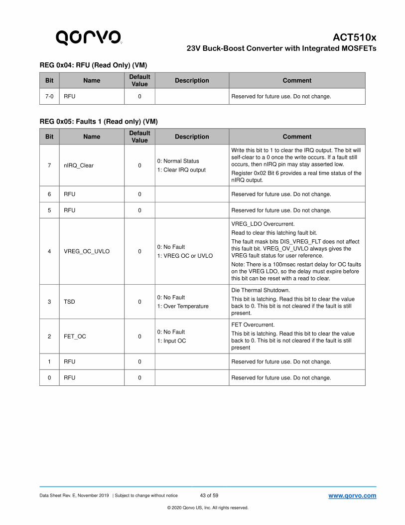
Data Sheet Rev. E, November 2019 | Subject to change without notice 43 of 59 www.qorvo.com
© 2020 Qorvo US, Inc. All rights reserved.
ACT510x
23V Buck-Boost Converter with Integrated MOSFETs
REG 0x04: RFU (Read Only) (VM)
Bit Name Default Value
Description Comment
7-0 RFU 0 Reserved for future use. Do not change.
REG 0x05: Faults 1 (Read only) (VM)
Bit Name Default Value
Description Comment
7 nIRQ_Clear 0 0: Normal Status
1: Clear IRQ output
Write this bit to 1 to clear the IRQ output. The bit will
self-clear to a 0 once the write occurs. If a fault still
occurs, then nIRQ pin may stay asserted low.
Register 0x02 Bit 6 provides a real time status of the
nIRQ output.
6 RFU 0 Reserved for future use. Do not change.
5 RFU 0 Reserved for future use. Do not change.
4 VREG_OC_UVLO 0 0: No Fault
1: VREG OC or UVLO
VREG_LDO Overcurrent.
Read to clear this latching fault bit.
The fault mask bits DIS_VREG_FLT does not affect
this fault bit. VREG_OV_UVLO always gives the
VREG fault status for user reference.
Note: There is a 100msec restart delay for OC faults
on the VREG LDO, so the delay must expire before
this bit can be reset with a read to clear.
3 TSD 0 0: No Fault
1: Over Temperature
Die Thermal Shutdown.
This bit is latching. Read this bit to clear the value
back to 0. This bit is not cleared if the fault is still
present.
2 FET_OC 0 0: No Fault
1: Input OC
FET Overcurrent.
This bit is latching. Read this bit to clear the value
back to 0. This bit is not cleared if the fault is still
present
1 RFU 0 Reserved for future use. Do not change.
0 RFU 0 Reserved for future use. Do not change.
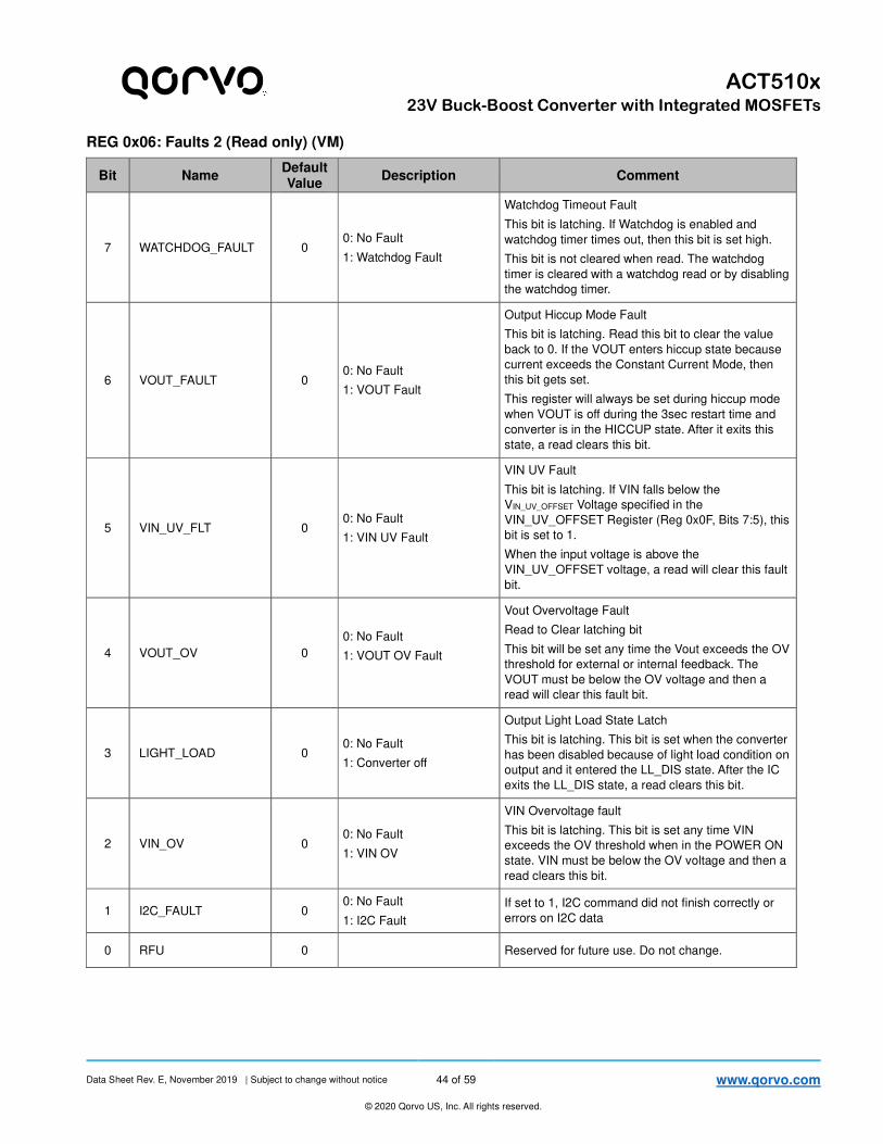
Data Sheet Rev. E, November 2019 | Subject to change without notice 44 of 59 www.qorvo.com
© 2020 Qorvo US, Inc. All rights reserved.
ACT510x
23V Buck-Boost Converter with Integrated MOSFETs
REG 0x06: Faults 2 (Read only) (VM)
Bit Name Default Value
Description Comment
7 WATCHDOG_FAULT 0 0: No Fault
1: Watchdog Fault
Watchdog Timeout Fault
This bit is latching. If Watchdog is enabled and
watchdog timer times out, then this bit is set high.
This bit is not cleared when read. The watchdog
timer is cleared with a watchdog read or by disabling
the watchdog timer.
6 VOUT_FAULT 0 0: No Fault
1: VOUT Fault
Output Hiccup Mode Fault
This bit is latching. Read this bit to clear the value
back to 0. If the VOUT enters hiccup state because
current exceeds the Constant Current Mode, then
this bit gets set.
This register will always be set during hiccup mode
when VOUT is off during the 3sec restart time and
converter is in the HICCUP state. After it exits this
state, a read clears this bit.
5 VIN_UV_FLT 0 0: No Fault
1: VIN UV Fault
VIN UV Fault
This bit is latching. If VIN falls below the
VIN_UV_OFFSET Voltage specified in the
VIN_UV_OFFSET Register (Reg 0x0F, Bits 7:5), this
bit is set to 1.
When the input voltage is above the
VIN_UV_OFFSET voltage, a read will clear this fault
bit.
4 VOUT_OV 0
0: No Fault
1: VOUT OV Fault
Vout Overvoltage Fault
Read to Clear latching bit
This bit will be set any time the Vout exceeds the OV
threshold for external or internal feedback. The
VOUT must be below the OV voltage and then a
read will clear this fault bit.
3 LIGHT_LOAD 0 0: No Fault
1: Converter off
Output Light Load State Latch
This bit is latching. This bit is set when the converter
has been disabled because of light load condition on
output and it entered the LL_DIS state. After the IC
exits the LL_DIS state, a read clears this bit.
2 VIN_OV 0 0: No Fault
1: VIN OV
VIN Overvoltage fault
This bit is latching. This bit is set any time VIN
exceeds the OV threshold when in the POWER ON
state. VIN must be below the OV voltage and then a
read clears this bit.
1 I2C_FAULT 0 0: No Fault
1: I2C Fault
If set to 1, I2C command did not finish correctly or
errors on I2C data
0 RFU 0 Reserved for future use. Do not change.
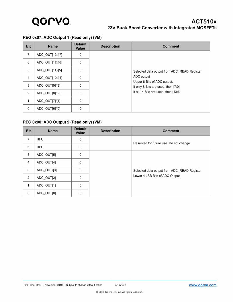
Data Sheet Rev. E, November 2019 | Subject to change without notice 45 of 59 www.qorvo.com
© 2020 Qorvo US, Inc. All rights reserved.
ACT510x
23V Buck-Boost Converter with Integrated MOSFETs
REG 0x07: ADC Output 1 (Read only) (VM)
Bit Name Default Value
Description Comment
7 ADC_OUT[13]/[7] 0
Selected data output from ADC_READ Register
ADC output
Upper 8 Bits of ADC output.
If only 8 Bits are used, then [7:0]
If all 14 Bits are used, then [13:6]
6 ADC_OUT[12]/[6] 0
5 ADC_OUT[11]/[5] 0
4 ADC_OUT[10]/[4] 0
3 ADC_OUT[9]/[3] 0
2 ADC_OUT[8]/[2] 0
1 ADC_OUT[7]/[1] 0
0 ADC_OUT[6]/[0] 0
REG 0x08: ADC Output 2 (Read only) (VM)
Bit Name Default Value
Description Comment
7 RFU 0 Reserved for future use. Do not change.
6 RFU 0
5 ADC_OUT[5] 0
Selected data output from ADC_READ Register
Lower 4 LSB Bits of ADC Output
4 ADC_OUT[4] 0
3 ADC_OUT/[3] 0
2 ADC_OUT[2] 0
1 ADC_OUT[1] 0
0 ADC_OUT[0] 0
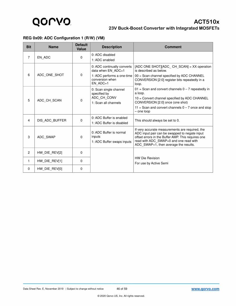
Data Sheet Rev. E, November 2019 | Subject to change without notice 46 of 59 www.qorvo.com
© 2020 Qorvo US, Inc. All rights reserved.
ACT510x
23V Buck-Boost Converter with Integrated MOSFETs
REG 0x09: ADC Configuration 1 (R/W) (VM)
Bit Name Default Value
Description Comment
7 EN_ADC 0 0: ADC disabled
1: ADC enabled
6 ADC_ONE_SHOT 0
0: ADC continually converts
data when EN_ADC=1
1: ADC performs a one-time conversion when EN_ADC=1
[ADC ONE SHOT][ADC_ CH_SCAN] = XX operation
is described as below.
00 = Scan channel specified by ADC CHANNEL
CONVERSION [2:0] register bits repeatedly in a
loop.
01 = Scan and convert channels 0 – 7 repeatedly in
a loop.
10 = Convert channel specified by ADC CHANNEL
CONVERSION [2:0] once (one shot)
11 = Scan and convert channels 0 – 7 once and stop – one loop
5 ADC_CH_SCAN 0
0: Scan single channel
specified by
ADC_CH_CONV
1: Scan all channels
4 DIS_ADC_BUFFER 0 0: ADC Buffer is enabled
1: ADC Buffer is disabled This should always be set to 0.
3 ADC_SWAP 0
0: ADC Buffer is normal
inputs
1: ADC Buffer swaps inputs
If very accurate measurements are required, the ADC input pair can be swapped to negate input offset errors in the Buffer AMP. This requires one read with ADC_SWAP=0 and one read with ADC_SWAP=1, then average the results.
2 HW_DIE_REV[2] 0
HW Die Revision
For use by Active Semi 1 HW_DIE_REV[1] 0
0 HW_DIE_REV[0] 0
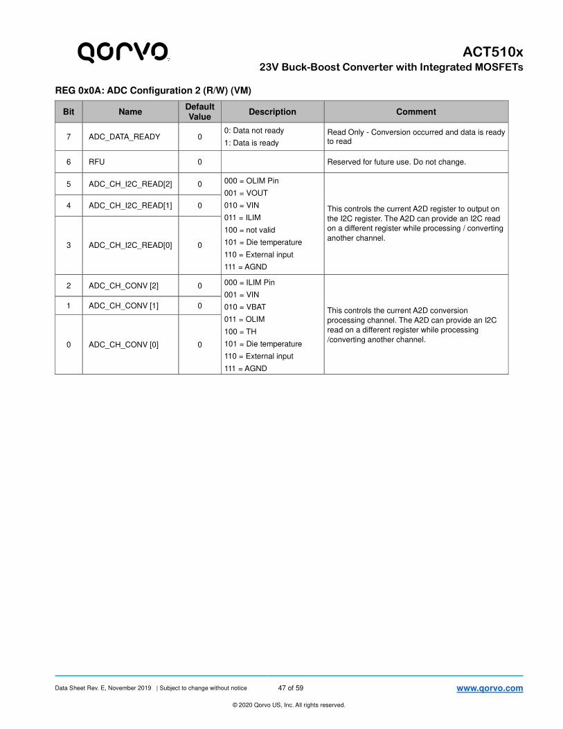
Data Sheet Rev. E, November 2019 | Subject to change without notice 47 of 59 www.qorvo.com
© 2020 Qorvo US, Inc. All rights reserved.
ACT510x
23V Buck-Boost Converter with Integrated MOSFETs
REG 0x0A: ADC Configuration 2 (R/W) (VM)
Bit Name Default Value
Description Comment
7 ADC_DATA_READY 0 0: Data not ready
1: Data is ready
Read Only - Conversion occurred and data is ready to read
6 RFU 0 Reserved for future use. Do not change.
5 ADC_CH_I2C_READ[2] 0 000 = OLIM Pin
001 = VOUT
010 = VIN
011 = ILIM
100 = not valid
101 = Die temperature
110 = External input
111 = AGND
This controls the current A2D register to output on
the I2C register. The A2D can provide an I2C read
on a different register while processing / converting
another channel.
4 ADC_CH_I2C_READ[1] 0
3 ADC_CH_I2C_READ[0] 0
2 ADC_CH_CONV [2] 0 000 = ILIM Pin
001 = VIN
010 = VBAT
011 = OLIM
100 = TH
101 = Die temperature
110 = External input
111 = AGND
This controls the current A2D conversion
processing channel. The A2D can provide an I2C
read on a different register while processing
/converting another channel.
1 ADC_CH_CONV [1] 0
0 ADC_CH_CONV [0] 0
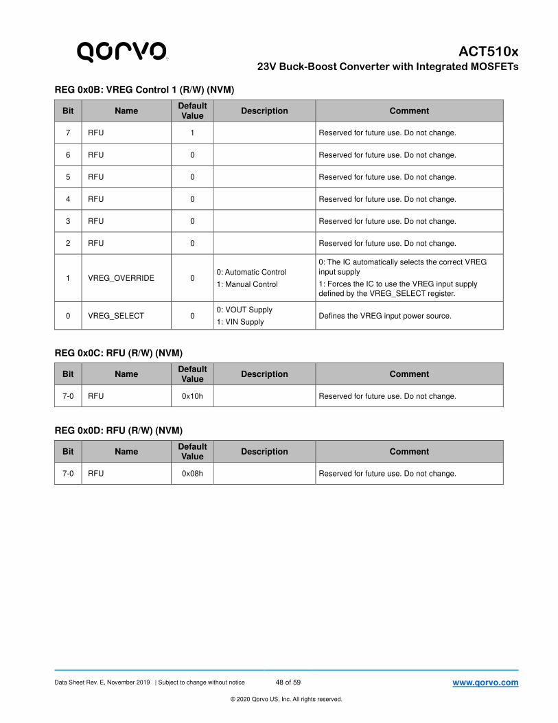
Data Sheet Rev. E, November 2019 | Subject to change without notice 48 of 59 www.qorvo.com
© 2020 Qorvo US, Inc. All rights reserved.
ACT510x
23V Buck-Boost Converter with Integrated MOSFETs
REG 0x0B: VREG Control 1 (R/W) (NVM)
Bit Name Default Value
Description Comment
7 RFU 1 Reserved for future use. Do not change.
6 RFU 0 Reserved for future use. Do not change.
5 RFU 0 Reserved for future use. Do not change.
4 RFU 0 Reserved for future use. Do not change.
3 RFU 0 Reserved for future use. Do not change.
2 RFU 0 Reserved for future use. Do not change.
1 VREG_OVERRIDE 0 0: Automatic Control
1: Manual Control
0: The IC automatically selects the correct VREG
input supply
1: Forces the IC to use the VREG input supply
defined by the VREG_SELECT register.
0 VREG_SELECT 0 0: VOUT Supply
1: VIN Supply Defines the VREG input power source.
REG 0x0C: RFU (R/W) (NVM)
Bit Name Default Value
Description Comment
7-0 RFU 0x10h Reserved for future use. Do not change.
REG 0x0D: RFU (R/W) (NVM)
Bit Name Default Value
Description Comment
7-0 RFU 0x08h Reserved for future use. Do not change.
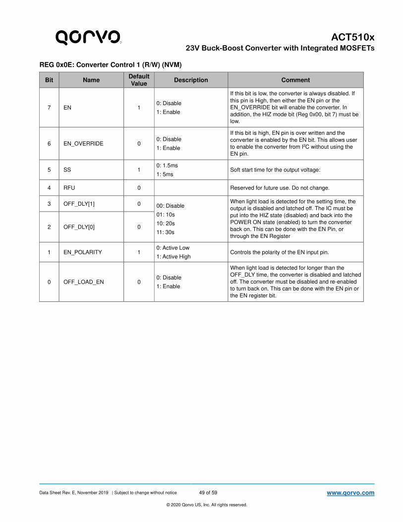
Data Sheet Rev. E, November 2019 | Subject to change without notice 49 of 59 www.qorvo.com
© 2020 Qorvo US, Inc. All rights reserved.
ACT510x
23V Buck-Boost Converter with Integrated MOSFETs
REG 0x0E: Converter Control 1 (R/W) (NVM)
Bit Name Default Value
Description Comment
7 EN 1 0: Disable
1: Enable
If this bit is low, the converter is always disabled. If
this pin is High, then either the EN pin or the
EN_OVERRIDE bit will enable the converter. In
addition, the HIZ mode bit (Reg 0x00, bit 7) must be
low.
6 EN_OVERRIDE 0 0: Disable
1: Enable
If this bit is high, EN pin is over written and the
converter is enabled by the EN bit. This allows user
to enable the converter from I2C without using the
EN pin.
5 SS 1 0: 1.5ms
1: 5ms Soft start time for the output voltage:
4 RFU 0 Reserved for future use. Do not change.
3 OFF_DLY[1] 0 00: Disable
01: 10s
10: 20s
11: 30s
When light load is detected for the setting time, the
output is disabled and latched off. The IC must be
put into the HIZ state (disabled) and back into the
POWER ON state (enabled) to turn the converter
back on. This can be done with the EN Pin, or
through the EN Register
2 OFF_DLY[0] 0
1 EN_POLARITY 1 0: Active Low
1: Active High Controls the polarity of the EN input pin.
0 OFF_LOAD_EN 0 0: Disable
1: Enable
When light load is detected for longer than the
OFF_DLY time, the converter is disabled and latched
off. The converter must be disabled and re-enabled
to turn back on. This can be done with the EN pin or
the EN register bit.
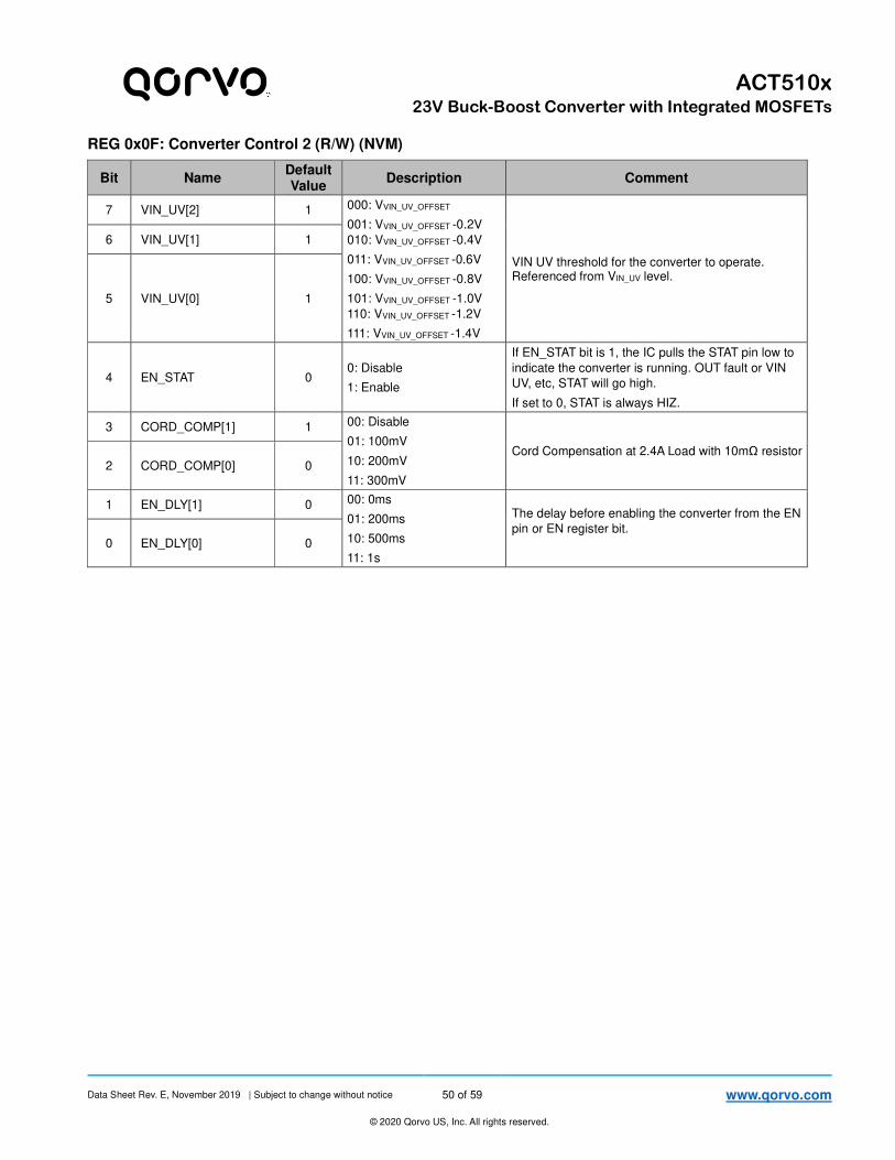
Data Sheet Rev. E, November 2019 | Subject to change without notice 50 of 59 www.qorvo.com
© 2020 Qorvo US, Inc. All rights reserved.
ACT510x
23V Buck-Boost Converter with Integrated MOSFETs
REG 0x0F: Converter Control 2 (R/W) (NVM)
Bit Name Default Value
Description Comment
7 VIN_UV[2] 1 000: VVIN_UV_OFFSET
001: VVIN_UV_OFFSET -0.2V
010: VVIN_UV_OFFSET -0.4V
011: VVIN_UV_OFFSET -0.6V
100: VVIN_UV_OFFSET -0.8V
101: VVIN_UV_OFFSET -1.0V
110: VVIN_UV_OFFSET -1.2V
111: VVIN_UV_OFFSET -1.4V
VIN UV threshold for the converter to operate. Referenced from VIN_UV level.
6 VIN_UV[1] 1
5 VIN_UV[0] 1
4 EN_STAT 0 0: Disable
1: Enable
If EN_STAT bit is 1, the IC pulls the STAT pin low to
indicate the converter is running. OUT fault or VIN
UV, etc, STAT will go high.
If set to 0, STAT is always HIZ.
3 CORD_COMP[1] 1 00: Disable
01: 100mV
10: 200mV
11: 300mV
Cord Compensation at 2.4A Load with 10mΩ resistor 2 CORD_COMP[0] 0
1 EN_DLY[1] 0 00: 0ms
01: 200ms
10: 500ms
11: 1s
The delay before enabling the converter from the EN
pin or EN register bit.
0 EN_DLY[0] 0

Data Sheet Rev. E, November 2019 | Subject to change without notice 51 of 59 www.qorvo.com
© 2020 Qorvo US, Inc. All rights reserved.
ACT510x
23V Buck-Boost Converter with Integrated MOSFETs
REG 0x10: Converter Control 3 (R/W) (NVM)
Bit Name Default Value
Description Comment
7 OUTPUT_SLEW[1] 0 00: 1V/ms
01: 0.5V/ms
10: 0.33V/ms
11: 0.1V/ms
For the ACT5101 only, when the output voltage is
changed using the VOUT register for QC2.0/3.0 or
USB PD voltage ramps, this register controls the
rate at which the output voltage changes. 6 OUTPUT_SLEW[0] 1
5 PULLDOWN_RAMP 1 0: Disable
1: Enable
If PULLDOWN_RAMP is set to 1 and VOUT_I2C is
set to 0 for I2C output voltage control (ACT5101), an
internal current source pulls down the output during
a ramp down of the output voltage. This allows the
output to meet the QC 2.0/3.0 and USB PD ramp
timing requirements.
4 PULLDOWN_OV 1 0: Disable
1: Enable
If PULLDOWN_OV is set to 1, the pulldown current
source pulls down on the output during any OV
condition on the output.
3 INPUT_ILIM[1] 1 00: Disable
01: 150% of IFCHG
10: 200% of IFCHG
11: 150% of IFCHG
The input current limit scaling factor relative to the
hardware programmed ILIM current setting. 2 INPUT_ILIM[0] 0
1 DIS_VREG_FLT 0 0: Enable
1: Disable
If set to 0, an Overcurrent or UVLO fault on the
VREG stops the buck-boost converter. If set to 1, the
buck-boost converter continues to operate with fault
on VREG.
0 DIS_PFM 0 0: Enable
1: Disable
Disable PFM mode in mode to set a fixed switching
frequency.
REG 0x11: VREG Regulation Voltage 1 (R/W) (NVM)
Bit Name Default Value
Description Comment
7 VREG[4] 1 1600mV
VREG LDO Output Voltage
Offset: 2V
Range: 2V (00000) - 5.1V (11111)
6 VREG[3] 1 800mV
5 VREG[2] 1 400mV
4 VREG[1] 1 200mV
3 VREG[0] 0 100mV
2 RFU 1 Reserved for future use. Do not change.
1 RFU 1 Reserved for future use. Do not change.
0 RFU 0 Reserved for future use. Do not change.
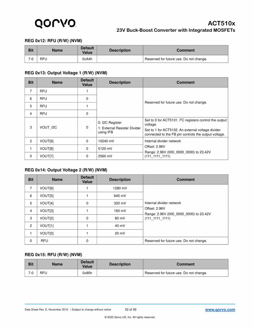
Data Sheet Rev. E, November 2019 | Subject to change without notice 52 of 59 www.qorvo.com
© 2020 Qorvo US, Inc. All rights reserved.
ACT510x
23V Buck-Boost Converter with Integrated MOSFETs
REG 0x12: RFU (R/W) (NVM)
Bit Name Default Value
Description Comment
7-0 RFU 0xA4h Reserved for future use. Do not change.
REG 0x13: Output Voltage 1 (R/W) (NVM)
Bit Name Default Value
Description Comment
7 RFU 1
Reserved for future use. Do not change. 6 RFU 0
5 RFU 1
4 RFU 0
3 VOUT_I2C 0
0: I2C Register
1: External Resister Divider using IFB
Set to 0 for ACT5101. I2C registers control the output
voltage.
Set to 1 for ACT5102. An external voltage divider
connected to the FB pin controls the output voltage.
2 VOUT[9] 0 10240 mV Internal divider network
Offset: 2.96V
Range: 2.96V (000_0000_0000) to 23.42V (111_1111_1111)
1 VOUT[8] 0 5120 mV
0 VOUT[7] 0 2560 mV
REG 0x14: Output Voltage 2 (R/W) (NVM)
Bit Name Default Value
Description Comment
7 VOUT[6] 1 1280 mV
Internal divider network
Offset: 2.96V
Range: 2.96V (000_0000_0000) to 23.42V
(111_1111_1111)
6 VOUT[5] 1 640 mV
5 VOUT[4] 0 320 mV
4 VOUT[3] 1 160 mV
3 VOUT[2] 0 80 mV
2 VOUT[1] 1 40 mV
1 VOUT[0] 1 20 mV
0 RFU 0 Reserved for future use. Do not change.
REG 0x15: RFU (R/W) (NVM)
Bit Name Default Value
Description Comment
7-0 RFU 0x80h Reserved for future use. Do not change.
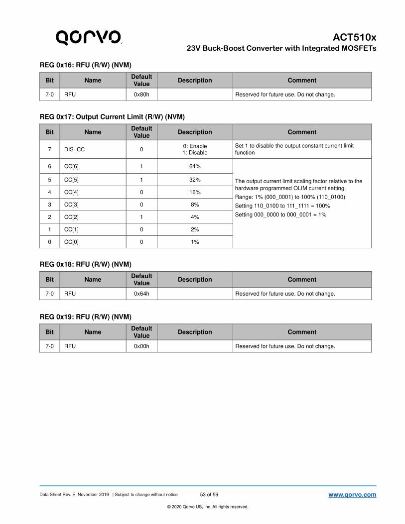
Data Sheet Rev. E, November 2019 | Subject to change without notice 53 of 59 www.qorvo.com
© 2020 Qorvo US, Inc. All rights reserved.
ACT510x
23V Buck-Boost Converter with Integrated MOSFETs
REG 0x16: RFU (R/W) (NVM)
Bit Name Default Value
Description Comment
7-0 RFU 0x80h Reserved for future use. Do not change.
REG 0x17: Output Current Limit (R/W) (NVM)
Bit Name Default Value
Description Comment
7 DIS_CC 0 0: Enable 1: Disable
Set 1 to disable the output constant current limit
function
6 CC[6] 1 64%
The output current limit scaling factor relative to the
hardware programmed OLIM current setting.
Range: 1% (000_0001) to 100% (110_0100)
Setting 110_0100 to 111_1111 = 100%
Setting 000_0000 to 000_0001 = 1%
5 CC[5] 1 32%
4 CC[4] 0 16%
3 CC[3] 0 8%
2 CC[2] 1 4%
1 CC[1] 0 2%
0 CC[0] 0 1%
REG 0x18: RFU (R/W) (NVM)
Bit Name Default Value
Description Comment
7-0 RFU 0x64h Reserved for future use. Do not change.
REG 0x19: RFU (R/W) (NVM)
Bit Name Default Value
Description Comment
7-0 RFU 0x00h Reserved for future use. Do not change.
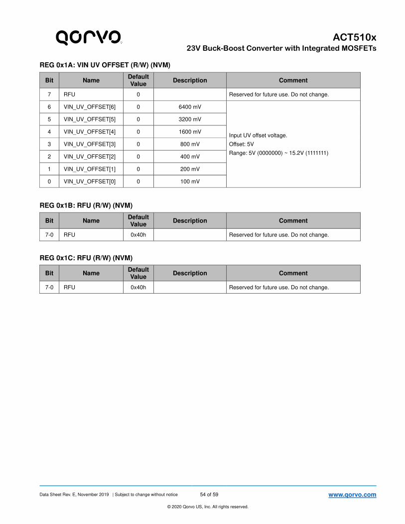
Data Sheet Rev. E, November 2019 | Subject to change without notice 54 of 59 www.qorvo.com
© 2020 Qorvo US, Inc. All rights reserved.
ACT510x
23V Buck-Boost Converter with Integrated MOSFETs
REG 0x1A: VIN UV OFFSET (R/W) (NVM)
Bit Name Default Value
Description Comment
7 RFU 0 Reserved for future use. Do not change.
6 VIN_UV_OFFSET[6] 0 6400 mV
Input UV offset voltage.
Offset: 5V
Range: 5V (0000000) ~ 15.2V (1111111)
5 VIN_UV_OFFSET[5] 0 3200 mV
4 VIN_UV_OFFSET[4] 0 1600 mV
3 VIN_UV_OFFSET[3] 0 800 mV
2 VIN_UV_OFFSET[2] 0 400 mV
1 VIN_UV_OFFSET[1] 0 200 mV
0 VIN_UV_OFFSET[0] 0 100 mV
REG 0x1B: RFU (R/W) (NVM)
Bit Name Default Value
Description Comment
7-0 RFU 0x40h Reserved for future use. Do not change.
REG 0x1C: RFU (R/W) (NVM)
Bit Name Default Value
Description Comment
7-0 RFU 0x40h Reserved for future use. Do not change.
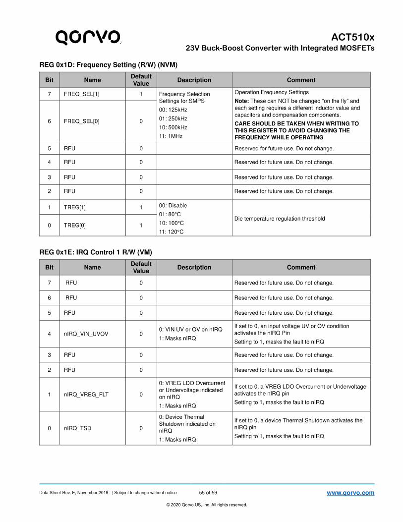
Data Sheet Rev. E, November 2019 | Subject to change without notice 55 of 59 www.qorvo.com
© 2020 Qorvo US, Inc. All rights reserved.
ACT510x
23V Buck-Boost Converter with Integrated MOSFETs
REG 0x1D: Frequency Setting (R/W) (NVM)
Bit Name Default Value
Description Comment
7 FREQ_SEL[1] 1 Frequency Selection
Settings for SMPS
00: 125kHz
01: 250kHz
10: 500kHz
11: 1MHz
Operation Frequency Settings
Note: These can NOT be changed “on the fly” and
each setting requires a different inductor value and
capacitors and compensation components.
CARE SHOULD BE TAKEN WHEN WRITING TO
THIS REGISTER TO AVOID CHANGING THE
FREQUENCY WHILE OPERATING
6 FREQ_SEL[0] 0
5 RFU 0 Reserved for future use. Do not change.
4 RFU 0 Reserved for future use. Do not change.
3 RFU 0 Reserved for future use. Do not change.
2 RFU 0 Reserved for future use. Do not change.
1 TREG[1] 1 00: Disable
01: 80°C
10: 100°C
11: 120°C
Die temperature regulation threshold
0 TREG[0] 1
REG 0x1E: IRQ Control 1 R/W (VM)
Bit Name Default Value
Description Comment
7 RFU 0 Reserved for future use. Do not change.
6 RFU 0 Reserved for future use. Do not change.
5 RFU 0 Reserved for future use. Do not change.
4 nIRQ_VIN_UVOV 0 0: VIN UV or OV on nIRQ
1: Masks nIRQ
If set to 0, an input voltage UV or OV condition
activates the nIRQ Pin
Setting to 1, masks the fault to nIRQ
3 RFU 0 Reserved for future use. Do not change.
2 RFU 0 Reserved for future use. Do not change.
1 nIRQ_VREG_FLT 0
0: VREG LDO Overcurrent
or Undervoltage indicated
on nIRQ
1: Masks nIRQ
If set to 0, a VREG LDO Overcurrent or Undervoltage
activates the nIRQ pin
Setting to 1, masks the fault to nIRQ
0 nIRQ_TSD 0
0: Device Thermal
Shutdown indicated on
nIRQ
1: Masks nIRQ
If set to 0, a device Thermal Shutdown activates the
nIRQ pin
Setting to 1, masks the fault to nIRQ
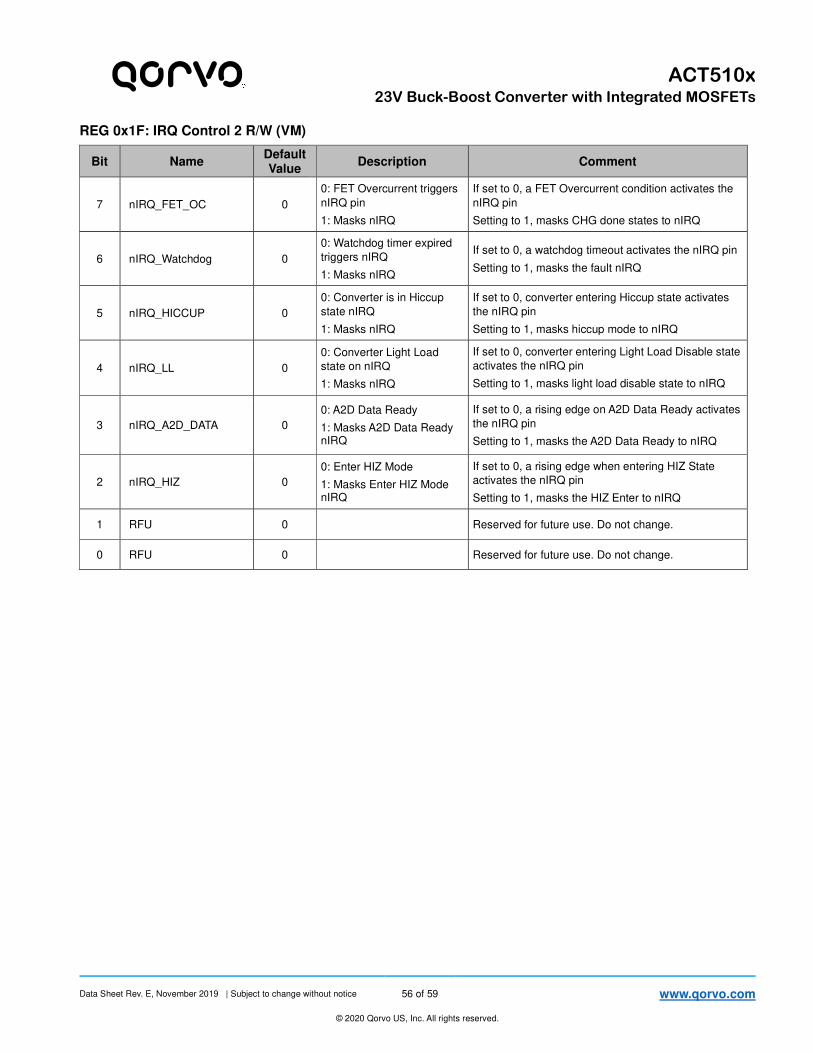
Data Sheet Rev. E, November 2019 | Subject to change without notice 56 of 59 www.qorvo.com
© 2020 Qorvo US, Inc. All rights reserved.
ACT510x
23V Buck-Boost Converter with Integrated MOSFETs
REG 0x1F: IRQ Control 2 R/W (VM)
Bit Name Default Value
Description Comment
7 nIRQ_FET_OC 0
0: FET Overcurrent triggers
nIRQ pin
1: Masks nIRQ
If set to 0, a FET Overcurrent condition activates the
nIRQ pin
Setting to 1, masks CHG done states to nIRQ
6 nIRQ_Watchdog 0
0: Watchdog timer expired
triggers nIRQ
1: Masks nIRQ
If set to 0, a watchdog timeout activates the nIRQ pin
Setting to 1, masks the fault nIRQ
5 nIRQ_HICCUP 0
0: Converter is in Hiccup
state nIRQ
1: Masks nIRQ
If set to 0, converter entering Hiccup state activates
the nIRQ pin
Setting to 1, masks hiccup mode to nIRQ
4 nIRQ_LL 0
0: Converter Light Load
state on nIRQ
1: Masks nIRQ
If set to 0, converter entering Light Load Disable state
activates the nIRQ pin
Setting to 1, masks light load disable state to nIRQ
3 nIRQ_A2D_DATA 0
0: A2D Data Ready
1: Masks A2D Data Ready nIRQ
If set to 0, a rising edge on A2D Data Ready activates
the nIRQ pin
Setting to 1, masks the A2D Data Ready to nIRQ
2 nIRQ_HIZ 0
0: Enter HIZ Mode
1: Masks Enter HIZ Mode nIRQ
If set to 0, a rising edge when entering HIZ State
activates the nIRQ pin
Setting to 1, masks the HIZ Enter to nIRQ
1 RFU 0 Reserved for future use. Do not change.
0 RFU 0 Reserved for future use. Do not change.
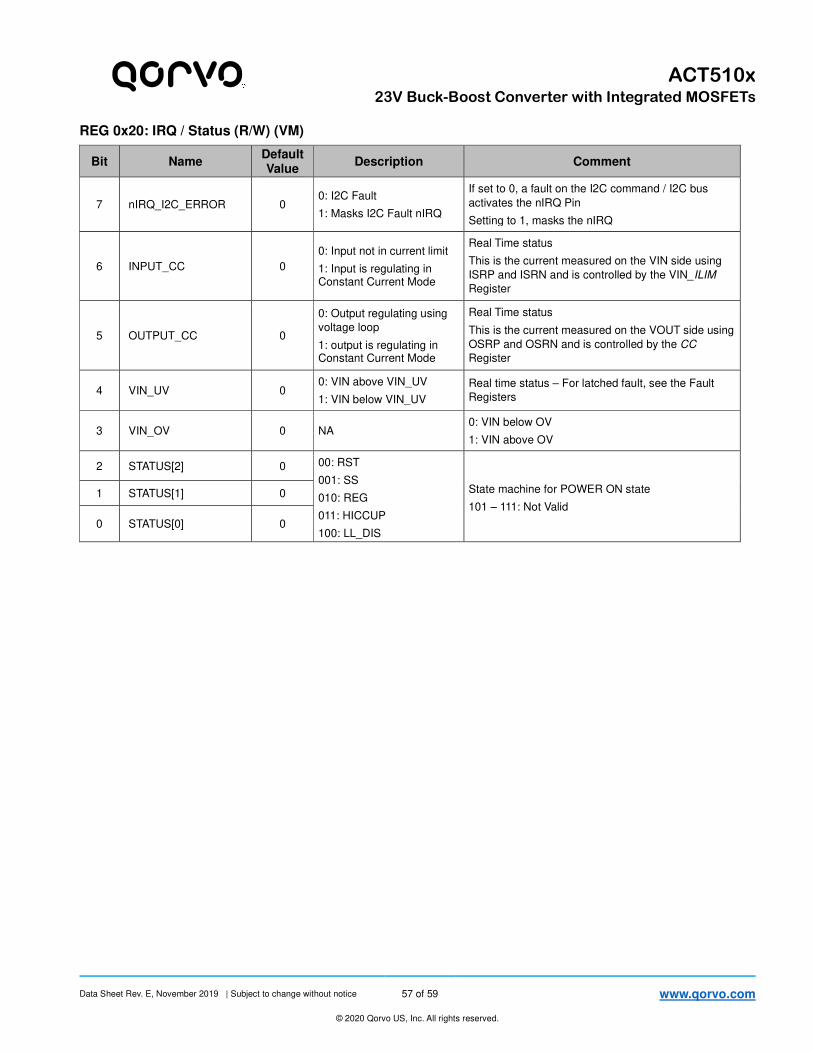
Data Sheet Rev. E, November 2019 | Subject to change without notice 57 of 59 www.qorvo.com
© 2020 Qorvo US, Inc. All rights reserved.
ACT510x
23V Buck-Boost Converter with Integrated MOSFETs
REG 0x20: IRQ / Status (R/W) (VM)
Bit Name Default Value
Description Comment
7 nIRQ_I2C_ERROR 0 0: I2C Fault
1: Masks I2C Fault nIRQ
If set to 0, a fault on the I2C command / I2C bus
activates the nIRQ Pin
Setting to 1, masks the nIRQ
6 INPUT_CC 0
0: Input not in current limit
1: Input is regulating in Constant Current Mode
Real Time status
This is the current measured on the VIN side using
ISRP and ISRN and is controlled by the VIN_ILIM
Register
5 OUTPUT_CC 0
0: Output regulating using
voltage loop
1: output is regulating in Constant Current Mode
Real Time status
This is the current measured on the VOUT side using
OSRP and OSRN and is controlled by the CC
Register
4 VIN_UV 0 0: VIN above VIN_UV
1: VIN below VIN_UV
Real time status – For latched fault, see the Fault
Registers
3 VIN_OV 0 NA 0: VIN below OV
1: VIN above OV
2 STATUS[2] 0 00: RST
001: SS
010: REG
011: HICCUP
100: LL_DIS
State machine for POWER ON state
101 – 111: Not Valid 1 STATUS[1] 0
0 STATUS[0] 0
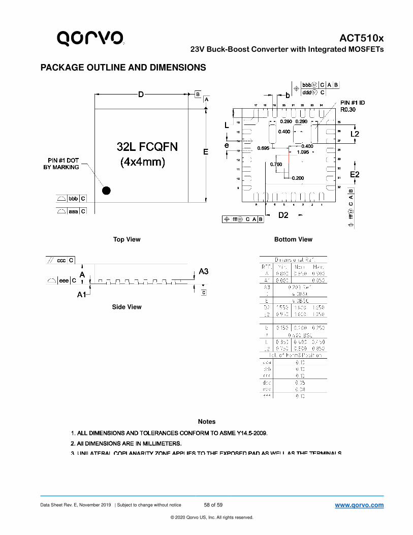
Data Sheet Rev. E, November 2019 | Subject to change without notice 58 of 59 www.qorvo.com
© 2020 Qorvo US, Inc. All rights reserved.
ACT510x
23V Buck-Boost Converter with Integrated MOSFETs
PACKAGE OUTLINE AND DIMENSIONS
Top View Bottom View
Side View
Notes
Data Sheet Rev. E, November 2019 | Subject to change without notice 59 of 59 www.qorvo.com
© 2020 Qorvo US, Inc. All rights reserved.
ACT510x
23V Buck-Boost Converter with Integrated MOSFETs
Contact Information
For the latest specifications, additional product information, worldwide sales and distribution locations:
Web: www.qorvo.com Tel: 1-844-890-8163
Email: [email protected]
For technical questions and application information:
Email: [email protected]
Important Notice
The information contained herein is believed to be reliable; however, Qorvo makes no warranties regarding the information contained
herein and assumes no responsibility or liability whatsoever for the use of the information contained herein. All information contained
herein is subject to change without notice. Customers should obtain and verify the latest relevant information before placing orders
for Qorvo products. The information contained herein or any use of such information does not grant, explicitly or implicitly, to any
party any patent rights, licenses, or any other intellectual property rights, whether with regard to such information itself or anything
described by such information. THIS INFORMATION DOES NOT CONSTITUTE A WARRANTY WITH RESPECT TO THE PROD-
UCTS DESCRIBED HEREIN, AND QORVO HEREBY DISCLAIMS ANY AND ALL WARRANTIES WITH RESPECT TO SUCH
PRODUCTS WHETHER EXPRESS OR IMPLIED BY LAW, COURSE OF DEALING, COURSE OF PERFORMANCE, USAGE OF
TRADE OR OTHERWISE, INCLUDING THE IMPLIED WARRANTIES OF MERCHANTABILITY AND FITNESS FOR A PARTICU-
LAR PURPOSE.
Without limiting the generality of the foregoing, Qorvo products are not warranted or authorized for use as critical components in
medical, life-saving, or life-sustaining applications, or other applications where a failure would reasonably be expected to cause
severe personal injury or death.
Copyright 2019 © Qorvo, Inc. | Qorvo® and Active-Semi® are trademarks of Qorvo, Inc.
Product Compliance
This part complies with RoHS directive 2011/65/EU as amended by (EU) 2015/863.
This part also has the following attributes:
• Lead Free
• Halogen Free (Chlorine, Bromine) Pb