Embed Size (px)
Citation preview

ACTEL CORPORATION
ACTEL TRAINING
VERILOG LAB GUIDE FOR LIBERO IDE ver2.3

A C T E L T R A I N I N G P R O G R A MV E R I L O G L A B G U I D E F O R L I B E R O I D E V E R 2 . 3
iiii
Introduction to the Actel Verilog Design Flow
IntroductionThis guide will take you through the design flow for Verilog using Actel Libero IDE version 2.3. Itexplains briefly how to use the software tools and provides information about the example design.
Actel Verilog Design Flow
Section
A C T E L T R A I N I N G P R O G R A MV E R I L O G L A B G U I D E F O R L I B E R O I D E V E R 2 . 3
2222
Overview
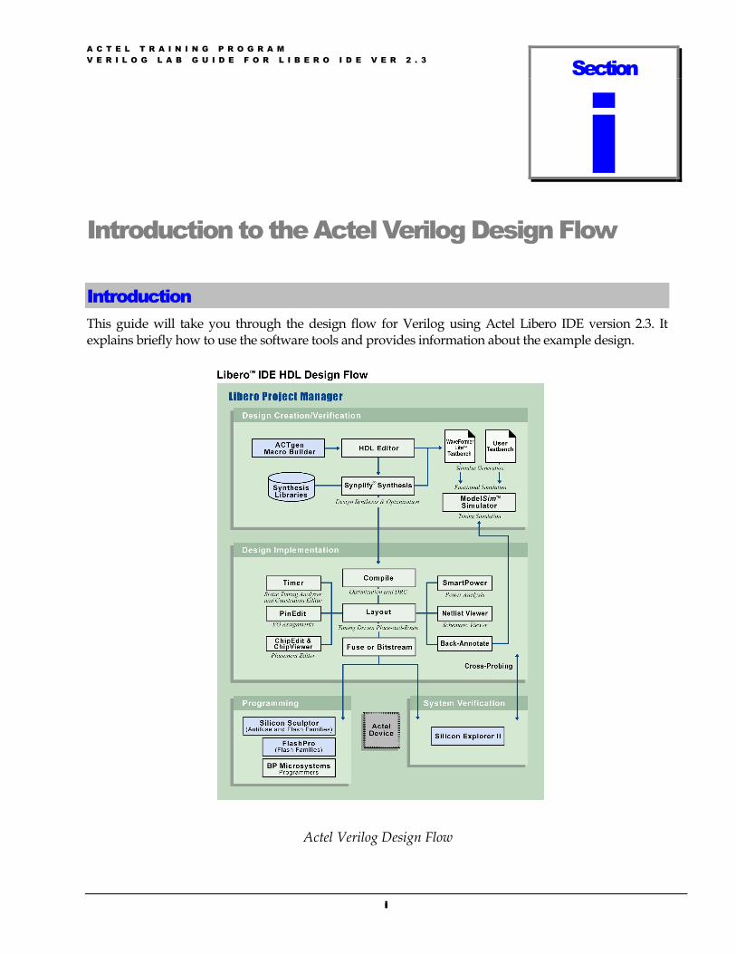
PurposeThe purpose of this lab is to become familiar with the Actel Verilog design flow. For this exercise, wewill implement a 16-bit loadable counter with an asynchronous reset and synchronous enable in anAX500 FPGA.
ToolsFor this lab, you will use the following tools:
• Libero IDE ver 2.3
• WaveFormer Lite 8.9
• ModelSim for Actel ver 5.6b
• Synplicity ver 7.2
• Designer R1-2003
Function16 bit synchronous counter triggered with the positive edge of the clock
Pin listENABLE = enable count active high
RESETn = asynchronous reset of the counter active low
CLK = master clock
LOAD = parallel load of the counter active high
DATA = 16 bit data input to counter
COUNT = 16 bit counter output
Counter block diagram
COUNTER
LOAD
DATA
16
16
COUNT
A C T E L T R A I N I N G P R O G R A MV E R I L O G L A B G U I D E F O R L I B E R O I D E V E R 2 . 3
3333
Creating a project in Libero IDE
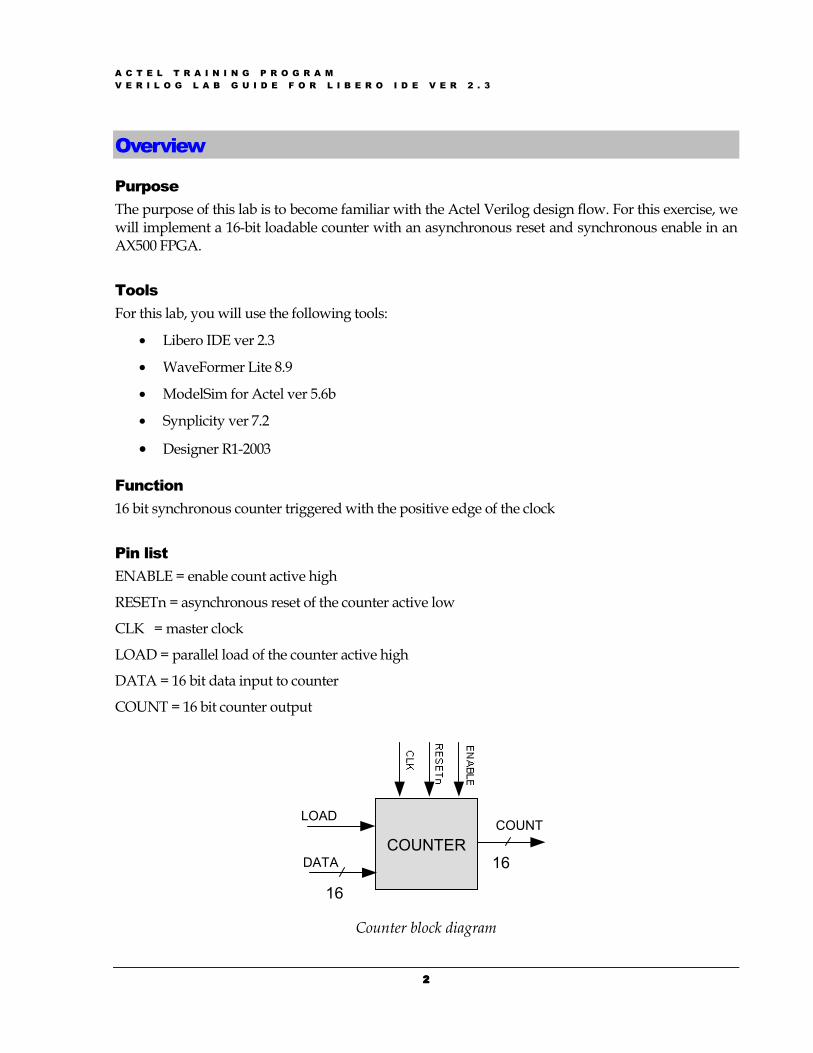
Creating a Libero IDE Project and entering the source fileStart Libero IDE by double clicking on the Actel Libero IDE shortcut on your desktop or by clickingStart > Programs > Libero IDE 2.3 > Libero IDE Design Environment.
From the File menu click New Project. The New Project dialog box appears, as shown.
Enter the following in the New Project dialog box:
Project Name: Enter counter16 in the Project Namefield (note that a folder named counter16 will becreated under the specified project location)
Location: Browse to C:\Actelprj
Family: Select Axcelerator from the Family drop-down list box
HDL: Select Verilog
Click OK. The project “counter16” is created andopened in Libero IDE.
Creating the Verilog source file
From the file menu, click New. In the New dialogbox, select Verilog Module and enter counter16 as thename. Click OK to open the HDL editor.
In the HDL editor, enter the description of a 16 bitcounter as described in the overview section.
Note: you can copy the description of the counterfrom Appendix A of this document and paste it intothe Libero IDE HDL editor.
Section
A C T E L T R A I N I N G P R O G R A MV E R I L O G L A B G U I D E F O R L I B E R O I D E V E R 2 . 3
4444
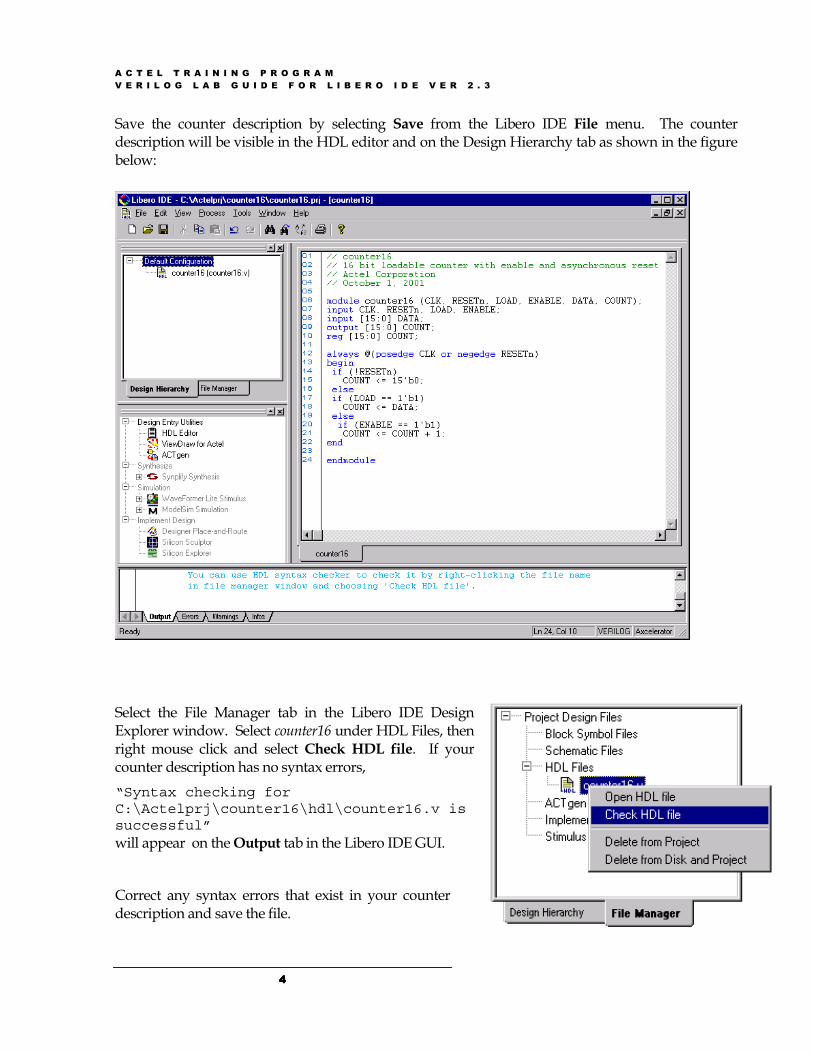
Save the counter description by selecting Save from the Libero IDE File menu. The counterdescription will be visible in the HDL editor and on the Design Hierarchy tab as shown in the figurebelow:
Select the File Manager tab in the Libero IDE DesignExplorer window. Select counter16 under HDL Files, thenright mouse click and select Check HDL file. If yourcounter description has no syntax errors,“Syntax checking forC:\Actelprj\counter16\hdl\counter16.v issuccessful”will appear on the Output tab in the Libero IDE GUI.
Correct any syntax errors that exist in your counterdescription and save the file.
A C T E L T R A I N I N G P R O G R A MV E R I L O G L A B G U I D E F O R L I B E R O I D E V E R 2 . 3
5555
Performing functional simulationIn this section you will generate stimulus for the counter and perform a functional (pre-synthesissimulation).
Creating Stimulus with WaveFormer Lite
WaveFormer Lite generates Verilog testbenches from drawn waveforms. There are three basic stepsfor creating test benches using WaveFormer Lite and Actel Libero IDE:
• Import Signal Information
• Draw WaveForms
• Export the Verilog Testbench
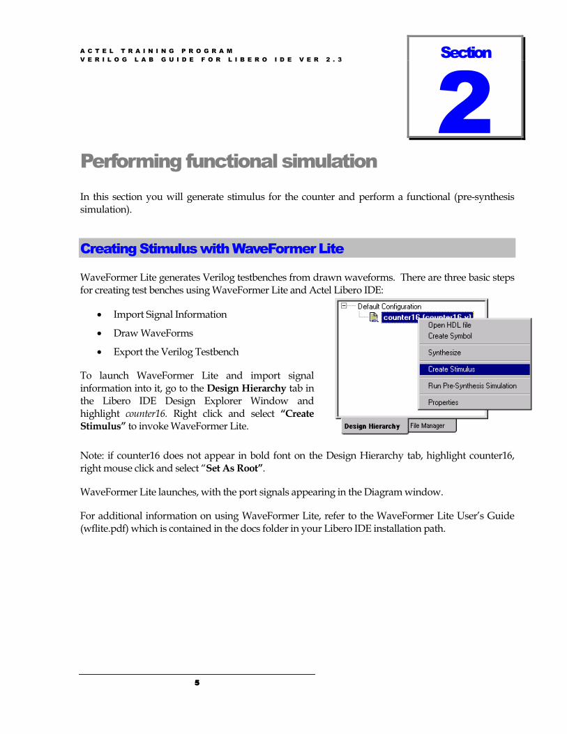
To launch WaveFormer Lite and import signalinformation into it, go to the Design Hierarchy tab inthe Libero IDE Design Explorer Window andhighlight counter16. Right click and select “CreateStimulus” to invoke WaveFormer Lite.
Note: if counter16 does not appear in bold font on the Design Hierarchy tab, highlight counter16,right mouse click and select “Set As Root”.
WaveFormer Lite launches, with the port signals appearing in the Diagram window.
For additional information on using WaveFormer Lite, refer to the WaveFormer Lite User’s Guide(wflite.pdf) which is contained in the docs folder in your Libero IDE installation path.
Section
A C T E L T R A I N I N G P R O G R A MV E R I L O G L A B G U I D E F O R L I B E R O I D E V E R 2 . 3
6666
Generating Stimulus for the Counter
In this step, you will generate stimulus and a testbench for the counter16 design using WaveFormerLite.
Create the clock signal by clicking the CLK signal in the diagram window then right mouse clickingand selecting “Signal(s) <-> Clock(s)”.
A Clock waveform will appear in the diagram window. Double click on the clock signal name in thediagram window to open the Signal Properties window. Click the Clock Properties button to openthe “Edit Clock Parameters” window. Specify the clock parameters to generate clock signals.
Using the instructions above, create a clock signal with the following properties:
• CLK - 100 MHz
• Starting Offset: 0 (default)
• Duty Cycle: 50% (default)
• Invert (starts low) unchecked
Accept defaults for all other clock parameters. Click OK to close the Clock Properties dialog box.
Click Apply then OK in the Signal Properties dialog box to create the clock waveform.
Draw waveforms for the other signals as listed below:
• RESETn - low 0 ns - 35 ns
high 35 ns - 1.2 us
• Load - low 0 ns - 775 ns
high 775 ns - 805 ns
low 775 ns - 1.2 us
• Enable - low 0 ns - 65 ns
high 65 ns - 1.2 us
• Data - 0000 0 ns - 765 ns
FFF8 765 ns - 1.2 us
Your waveforms should appear as shown in the figure on the next page.

A C T E L T R A I N I N G P R O G R A MV E R I L O G L A B G U I D E F O R L I B E R O I D E V E R 2 . 3
7777
WaveFormer Lite Diagram Window
Save the timing diagram by clicking Save from theWaveFormer Lite File menu.
In the Save As dialog box, enter counter16.btim as thefile name then click Save to save the timing diagram.
Generate the Verilog testbench by selecting ExportTiming Diagrams As (Export menu). In the Save Asdialog box, select Verilog Top Level TestBench (*.v)in the "Save As Type" pull-down menu. Entercounter16_tb.v in the filename box and click Save togenerate the testbench. After WaveFormer Litecreates the file, it will display its contents in the Reportwindow so that you can quickly verify that the file iscorrect.
Exit WaveFormer Lite by selecting Exit (File menu).Select Yes when prompted about closing all text files.
The waveform file and the testbench will appear onthe File Manager tab in the Libero IDE DesignExplorer window.

A C T E L T R A I N I N G P R O G R A MV E R I L O G L A B G U I D E F O R L I B E R O I D E V E R 2 . 3
8888
Performing pre-synthesis simulation with ModelSim for ActelTo perform pre-synthesis simulation, double click the ModelSim Simulation button in theLibero IDE Process window, or right mouse click on counter16 (Design Hierarchy tab) in the DesignExplorer Window and select Run Pre-Synthesis Simulation.
A dialog box will open indicating that no testbenchstimulus is associated with counter16. Select theAssociate stimulus radio button and click OK.
In the Select Stimulus dialog box, highlightcounter16_tb.v and click Add to add the testbench tothe Associated Files box.
Click OK to close the Select Stimulus dialog box andlaunch the ModelSim for Actel simulator.
The ModelSim for Actel Verilog Simulator will open and compile the source file and the testbench.
A C T E L T R A I N I N G P R O G R A MV E R I L O G L A B G U I D E F O R L I B E R O I D E V E R 2 . 3
9999
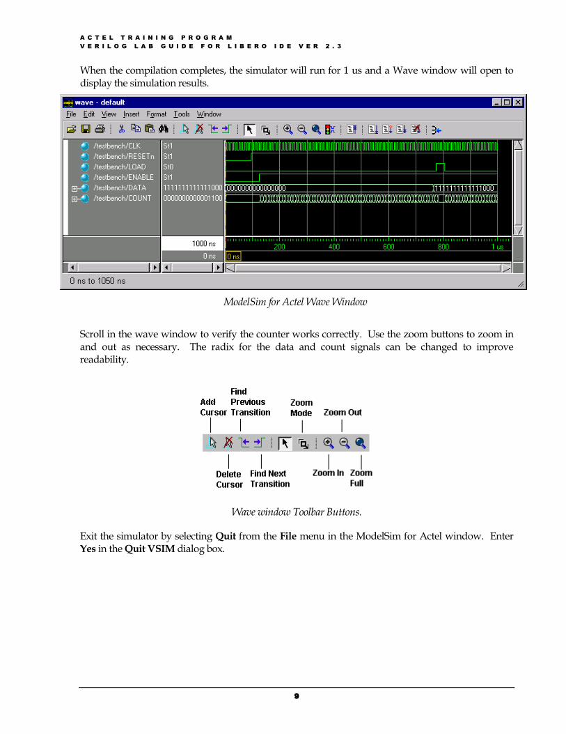
When the compilation completes, the simulator will run for 1 us and a Wave window will open todisplay the simulation results.
ModelSim for Actel Wave Window
Scroll in the wave window to verify the counter works correctly. Use the zoom buttons to zoom inand out as necessary. The radix for the data and count signals can be changed to improvereadability.
Wave window Toolbar Buttons.
Exit the simulator by selecting Quit from the File menu in the ModelSim for Actel window. EnterYes in the Quit VSIM dialog box.

A C T E L T R A I N I N G P R O G R A MV E R I L O G L A B G U I D E F O R L I B E R O I D E V E R 2 . 3
10101010
A C T E L T R A I N I N G P R O G R A MV E R I L O G L A B G U I D E F O R L I B E R O I D E V E R 2 . 3
11111111
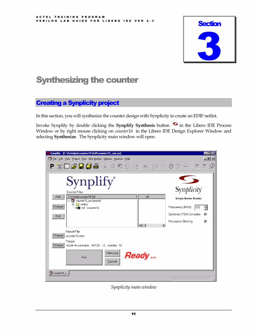
Synthesizing the counter
Creating a Synplicity project
In this section, you will synthesize the counter design with Synplicity to create an EDIF netlist.
Invoke Synplify by double clicking the Synplify Synthesis button in the Libero IDE ProcessWindow or by right mouse clicking on counter16 in the Libero IDE Design Explorer Window andselecting Synthesize. The Synplicity main window will open.
Synplicity main window
Section

A C T E L T R A I N I N G P R O G R A MV E R I L O G L A B G U I D E F O R L I B E R O I D E V E R 2 . 3
12121212
Change the target device by clicking the Change button.
The "Options for Implementation: counter16_syn: hdl" dialog box will open. In the device tab,confirm the following are set and click OK:
• Technology: Actel Axcelerator
• Part: AX500
• Speed Grade: -3
• Fanout Guide: 10 (default)
• Hard Limit to Fanout: off (unchecked)
• Disable I/O Insertion: off (default).
In Synplicity’s main window:
• Set the Frequency to 100 MHz
• Turn resource sharing off (unchecked)
• Symbolic FSM Compiler turned off (unchecked)
Click the RUN button. Synplify will now compile andsynthesize the counter16 design into a file calledcounter16.edn. When the Ready… on the main userinterface in Synplify changes to Done… the designhas been successfully mapped to the Axceleratorfamily.
The resultant EDIF file, counter16.edn, and a structuralVerilog netlist will be visible under ImplementationFiles on the Libero IDE File Manager tab in the DesignExplorer Window.
Click on the View Log button and scroll through the log file to answer the following questions:
Utilization
Combinational Cells: ___________ Sequential Cells: ____________
Frequency
Estimate Frequency:___________ MHz _________ ns
A C T E L T R A I N I N G P R O G R A MV E R I L O G L A B G U I D E F O R L I B E R O I D E V E R 2 . 3
13131313
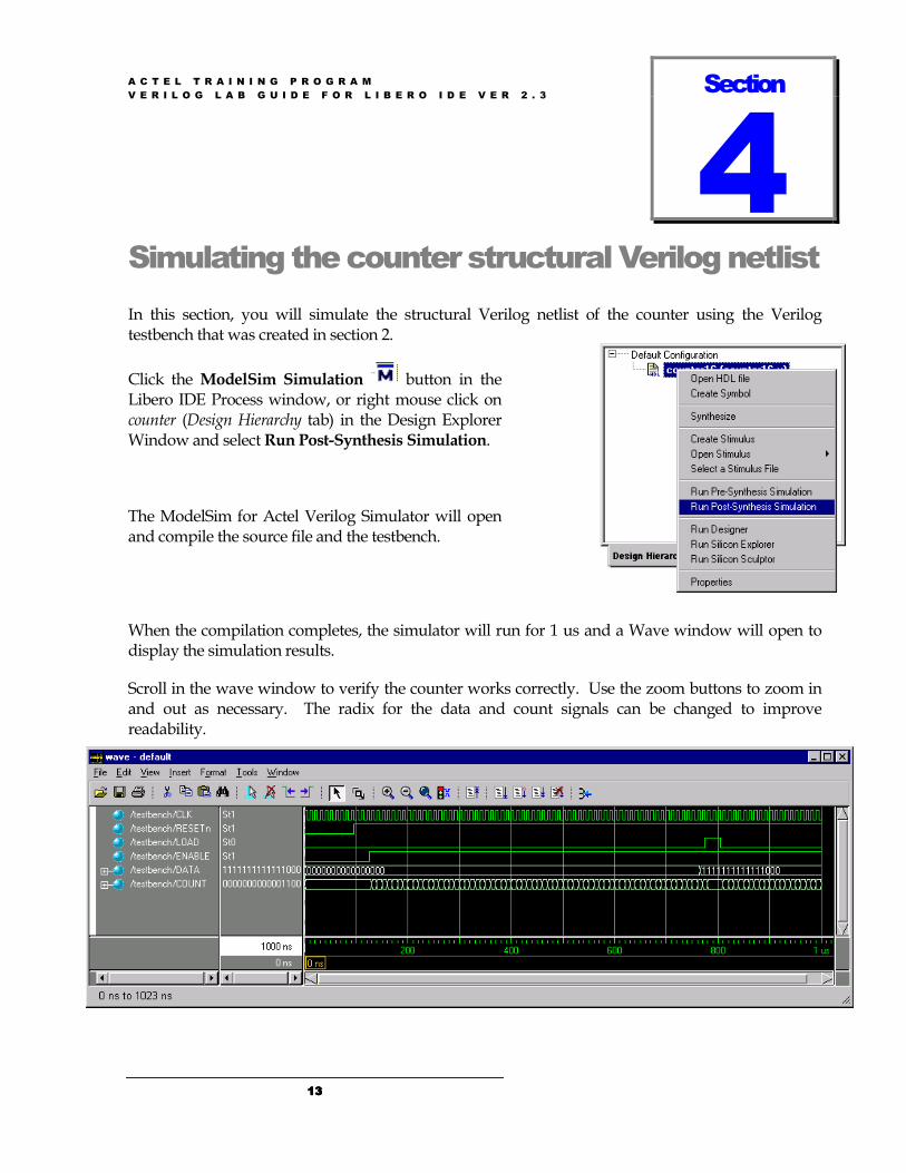
Simulating the counter structural Verilog netlistIn this section, you will simulate the structural Verilog netlist of the counter using the Verilogtestbench that was created in section 2.
Click the ModelSim Simulation button in theLibero IDE Process window, or right mouse click oncounter (Design Hierarchy tab) in the Design ExplorerWindow and select Run Post-Synthesis Simulation.
The ModelSim for Actel Verilog Simulator will openand compile the source file and the testbench.
When the compilation completes, the simulator will run for 1 us and a Wave window will open todisplay the simulation results.
Scroll in the wave window to verify the counter works correctly. Use the zoom buttons to zoom inand out as necessary. The radix for the data and count signals can be changed to improvereadability.
Section

A C T E L T R A I N I N G P R O G R A MV E R I L O G L A B G U I D E F O R L I B E R O I D E V E R 2 . 3
14141414
A C T E L T R A I N I N G P R O G R A MV E R I L O G L A B G U I D E F O R L I B E R O I D E V E R 2 . 3
15151515
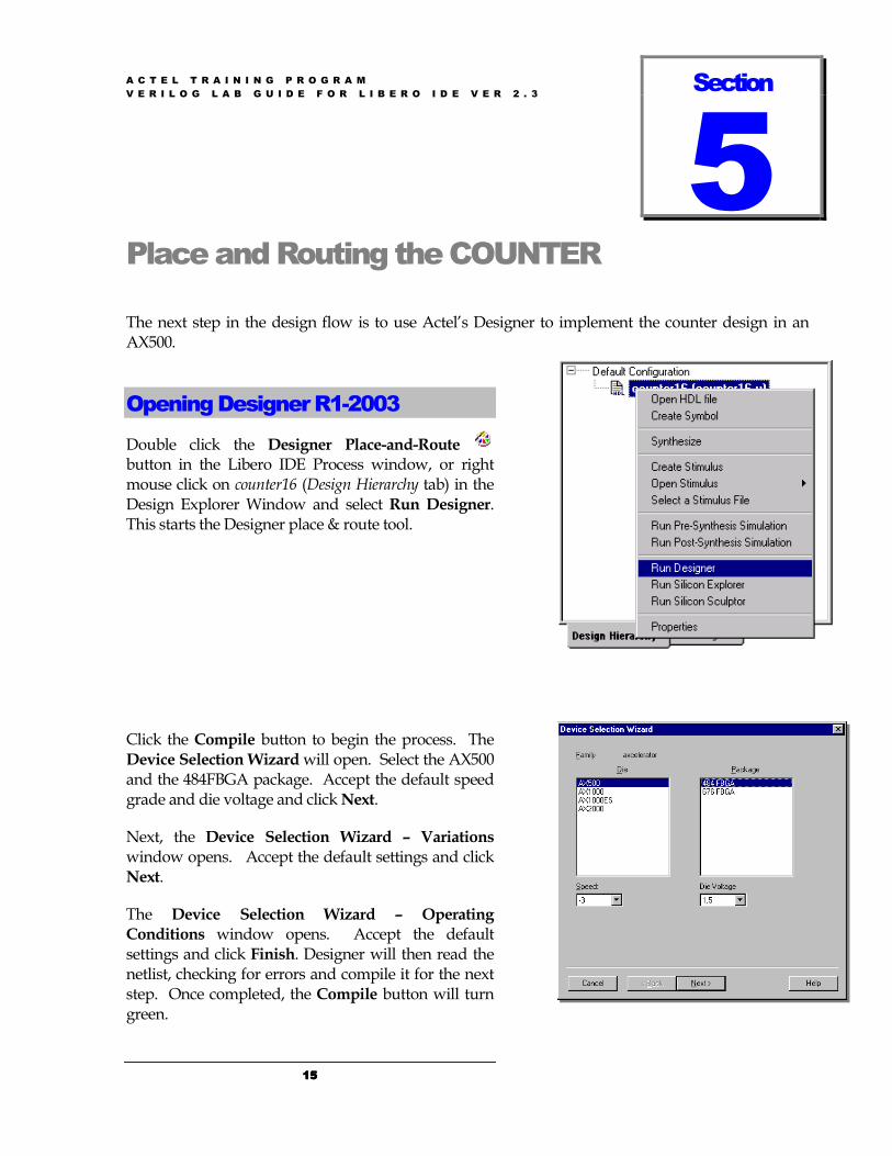
Place and Routing the COUNTER
The next step in the design flow is to use Actel’s Designer to implement the counter design in anAX500.
Opening Designer R1-2003
Double click the Designer Place-and-Route button in the Libero IDE Process window, or rightmouse click on counter16 (Design Hierarchy tab) in theDesign Explorer Window and select Run Designer.This starts the Designer place & route tool.
Click the Compile button to begin the process. TheDevice Selection Wizard will open. Select the AX500and the 484FBGA package. Accept the default speedgrade and die voltage and click Next.
Next, the Device Selection Wizard – Variationswindow opens. Accept the default settings and clickNext.
The Device Selection Wizard – OperatingConditions window opens. Accept the defaultsettings and click Finish. Designer will then read thenetlist, checking for errors and compile it for the nextstep. Once completed, the Compile button will turngreen.
Section

A C T E L T R A I N I N G P R O G R A MV E R I L O G L A B G U I D E F O R L I B E R O I D E V E R 2 . 3
16161616
Designer GUI after compiling the counter16 design
A C T E L T R A I N I N G P R O G R A MV E R I L O G L A B G U I D E F O R L I B E R O I D E V E R 2 . 3
17171717
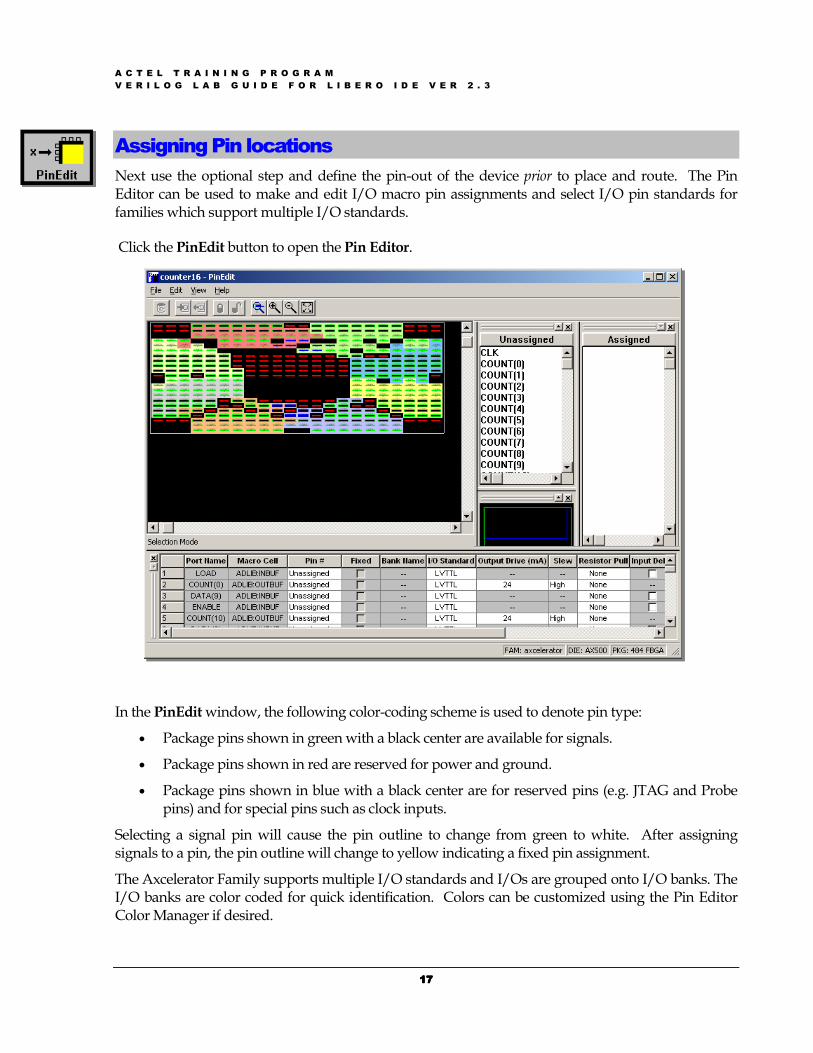
Assigning Pin locationsNext use the optional step and define the pin-out of the device prior to place and route. The PinEditor can be used to make and edit I/O macro pin assignments and select I/O pin standards forfamilies which support multiple I/O standards.
Click the PinEdit button to open the Pin Editor.
In the PinEdit window, the following color-coding scheme is used to denote pin type:
• Package pins shown in green with a black center are available for signals.
• Package pins shown in red are reserved for power and ground.
• Package pins shown in blue with a black center are for reserved pins (e.g. JTAG and Probepins) and for special pins such as clock inputs.
Selecting a signal pin will cause the pin outline to change from green to white. After assigningsignals to a pin, the pin outline will change to yellow indicating a fixed pin assignment.
The Axcelerator Family supports multiple I/O standards and I/Os are grouped onto I/O banks. TheI/O banks are color coded for quick identification. Colors can be customized using the Pin EditorColor Manager if desired.
A C T E L T R A I N I N G P R O G R A MV E R I L O G L A B G U I D E F O R L I B E R O I D E V E R 2 . 3
18181818
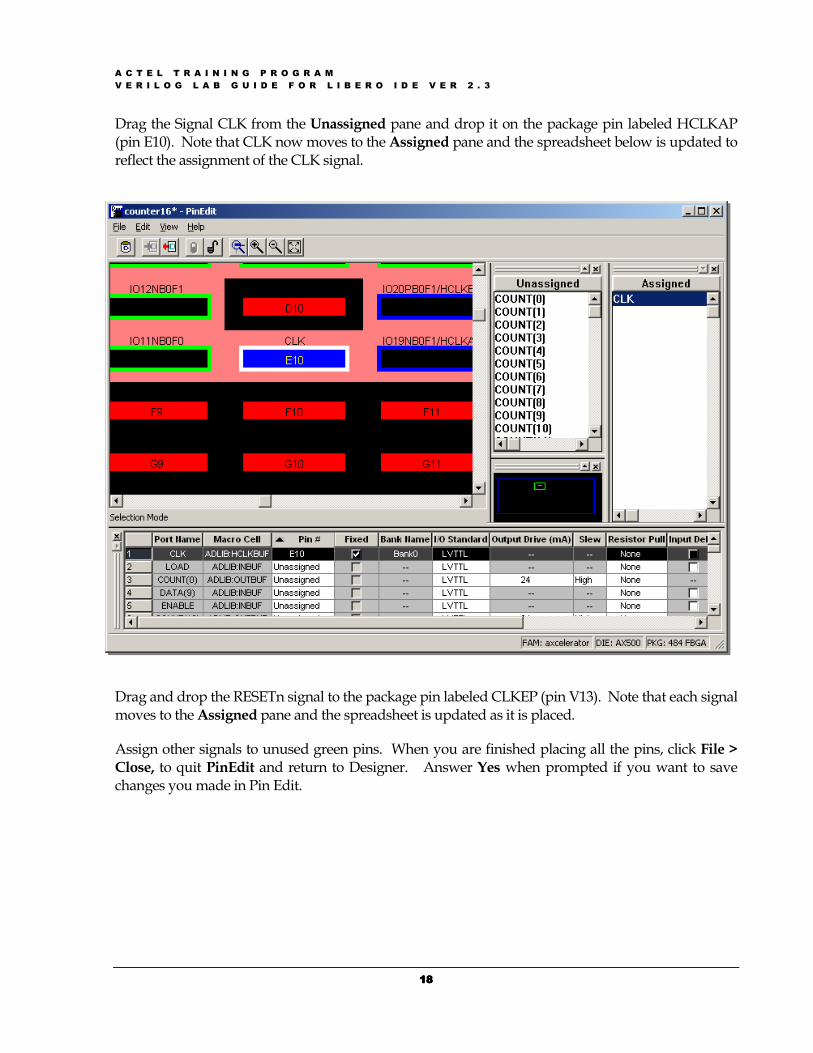
Drag the Signal CLK from the Unassigned pane and drop it on the package pin labeled HCLKAP(pin E10). Note that CLK now moves to the Assigned pane and the spreadsheet below is updated toreflect the assignment of the CLK signal.
Drag and drop the RESETn signal to the package pin labeled CLKEP (pin V13). Note that each signalmoves to the Assigned pane and the spreadsheet is updated as it is placed.
Assign other signals to unused green pins. When you are finished placing all the pins, click File >Close, to quit PinEdit and return to Designer. Answer Yes when prompted if you want to savechanges you made in Pin Edit.
A C T E L T R A I N I N G P R O G R A MV E R I L O G L A B G U I D E F O R L I B E R O I D E V E R 2 . 3
19191919
LayoutNow you will place and route the counter design – 100% automatically. To invoke the place & routetool, click the Layout button. Accept the default settings in the Layout Options window and clickOK. If you had added timing constraints, the Timing-Driven option would be available. For designswhich were previously place & routed that have minor changes, you could select On or Fix underthe Incremental options in the Layout window.
Layout will place and route our design, and the Layout button will turn green when completed.
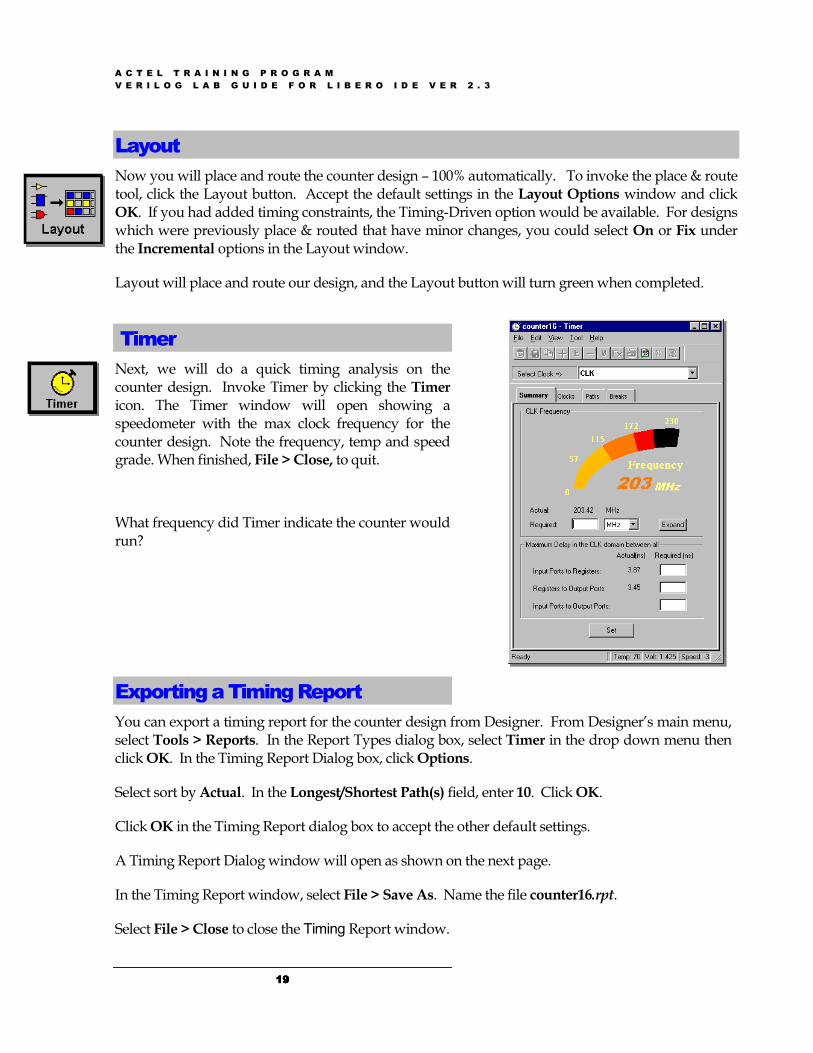
TimerNext, we will do a quick timing analysis on thecounter design. Invoke Timer by clicking the Timericon. The Timer window will open showing aspeedometer with the max clock frequency for thecounter design. Note the frequency, temp and speedgrade. When finished, File > Close, to quit.
What frequency did Timer indicate the counter wouldrun?
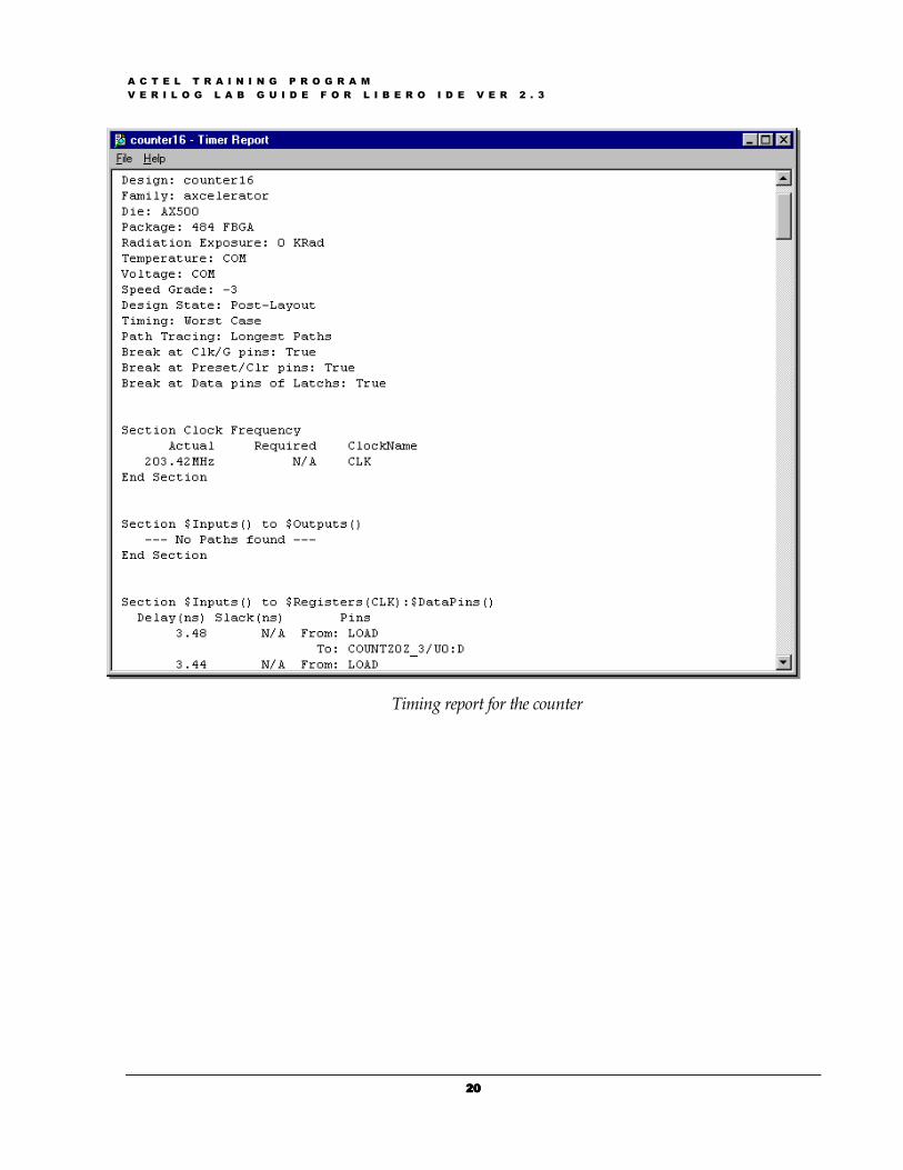
Exporting a Timing ReportYou can export a timing report for the counter design from Designer. From Designer’s main menu,select Tools > Reports. In the Report Types dialog box, select Timer in the drop down menu thenclick OK. In the Timing Report Dialog box, click Options.
Select sort by Actual. In the Longest/Shortest Path(s) field, enter 10. Click OK.
Click OK in the Timing Report dialog box to accept the other default settings.
A Timing Report Dialog window will open as shown on the next page.
In the Timing Report window, select File > Save As. Name the file counter16.rpt.
Select File > Close to close the Timing Report window.
A C T E L T R A I N I N G P R O G R A MV E R I L O G L A B G U I D E F O R L I B E R O I D E V E R 2 . 3
20202020
Timing report for the counter

A C T E L T R A I N I N G P R O G R A MV E R I L O G L A B G U I D E F O R L I B E R O I D E V E R 2 . 3
21212121
Back-annotate To do timing simulation using post-layout results,you need to generate the necessary files: post-placement netlist and an SDF (Standard DelayFormat) file with actual timing numbers from ourplace & route. Click the Back-Annotate button andthe Back-Annotate window will open.
Accept all defaults and click OK (see figure to right).
Saving your design files Be sure the save your work! When finished, click File> Save then File > Exit, to close Designer.
After exiting Designer, the Actel database(counter16.adb) and the timing information(counter16_ba.sdf) will be visible in the Libero IDEDesign Explorer window on the File manager tabunder Implementation Files.

A C T E L T R A I N I N G P R O G R A MV E R I L O G L A B G U I D E F O R L I B E R O I D E V E R 2 . 3
22222222
A C T E L T R A I N I N G P R O G R A MV E R I L O G L A B G U I D E F O R L I B E R O I D E V E R 2 . 3
23232323
Back-Annotated Timing Simulation
Invoking the SimulatorIn this section, you will simulate the structural Verilog netlist of the counter using the Verilogtestbench that was created in section 2 and the actual timing numbers (SDF) exported from Designerin section 5.
Click the ModelSim Simulation button in theLibero IDE Process window, or right mouse click oncounter16 (Design Hierarchy tab) in the Design ExplorerWindow and select Run Post-Layout Simulation.
The ModelSim for Actel Verilog Simulator will openand compile the source file and the testbench.
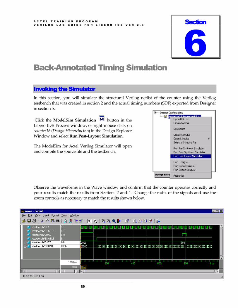
Observe the waveforms in the Wave window and confirm that the counter operates correctly andyour results match the results from Sections 2 and 4. Change the radix of the signals and use thezoom controls as necessary to match the results shown below.
Section
A C T E L T R A I N I N G P R O G R A MV E R I L O G L A B G U I D E F O R L I B E R O I D E V E R 2 . 3
24242424
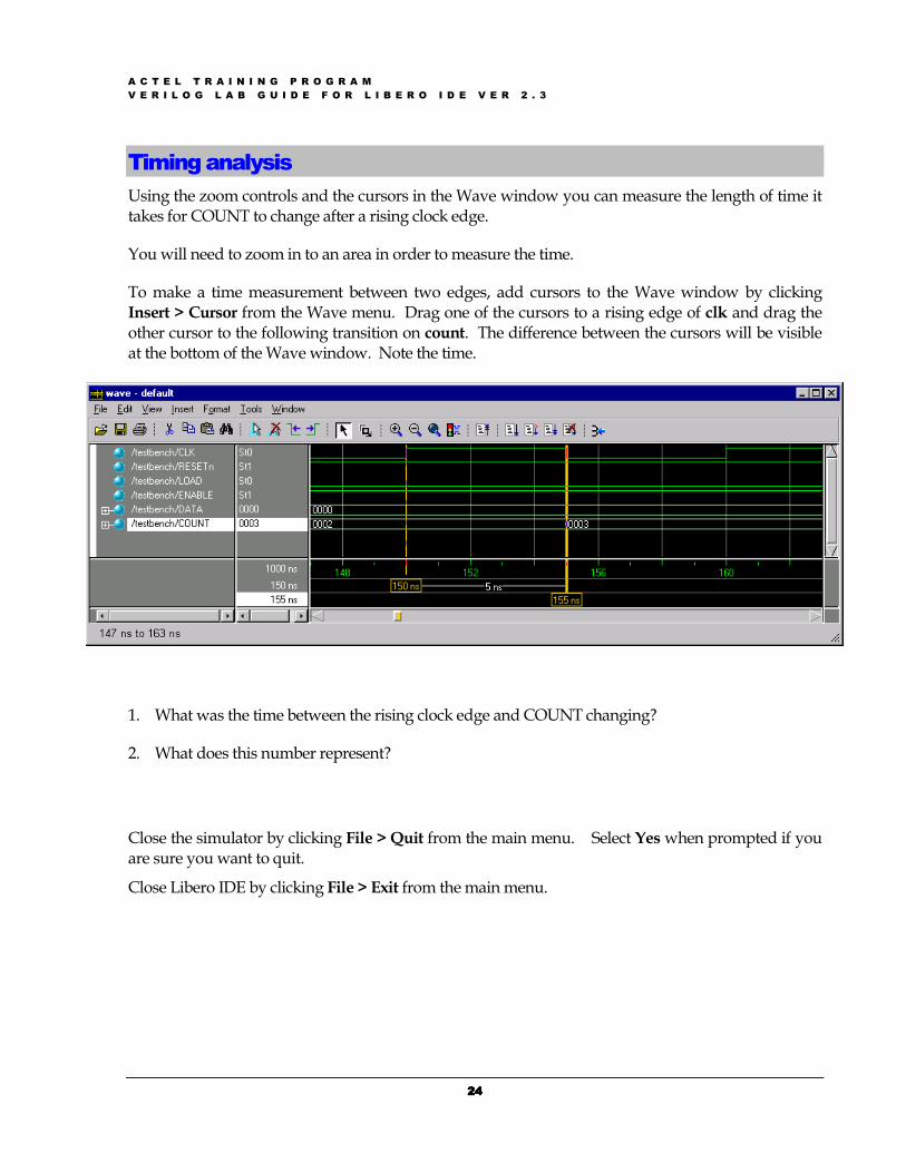
Timing analysisUsing the zoom controls and the cursors in the Wave window you can measure the length of time ittakes for COUNT to change after a rising clock edge.
You will need to zoom in to an area in order to measure the time.
To make a time measurement between two edges, add cursors to the Wave window by clickingInsert > Cursor from the Wave menu. Drag one of the cursors to a rising edge of clk and drag theother cursor to the following transition on count. The difference between the cursors will be visibleat the bottom of the Wave window. Note the time.
1. What was the time between the rising clock edge and COUNT changing?
2. What does this number represent?
Close the simulator by clicking File > Quit from the main menu. Select Yes when prompted if youare sure you want to quit.
Close Libero IDE by clicking File > Exit from the main menu.
A C T E L T R A I N I N G P R O G R A MV E R I L O G L A B G U I D E F O R L I B E R O I D E V E R 2 . 3
25252525
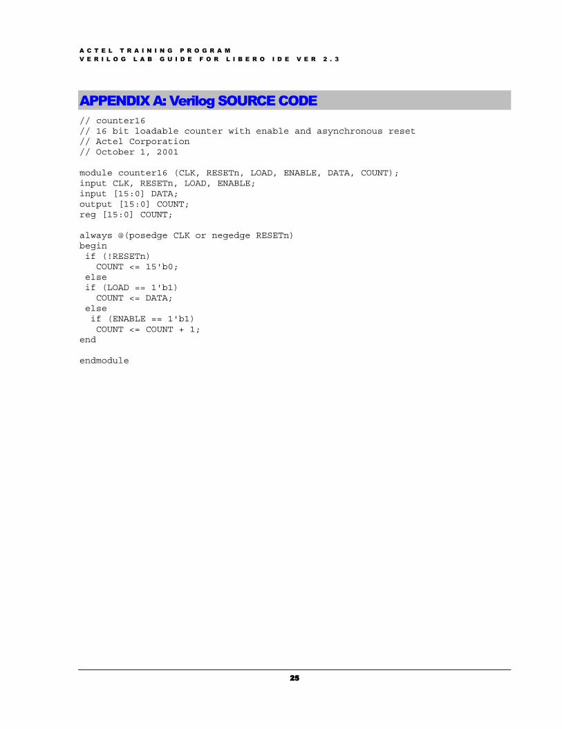
APPENDIX A: Verilog SOURCE CODE// counter16// 16 bit loadable counter with enable and asynchronous reset// Actel Corporation// October 1, 2001
module counter16 (CLK, RESETn, LOAD, ENABLE, DATA, COUNT);input CLK, RESETn, LOAD, ENABLE;input [15:0] DATA;output [15:0] COUNT;reg [15:0] COUNT;
always @(posedge CLK or negedge RESETn)beginif (!RESETn)
COUNT <= 15'b0;elseif (LOAD == 1'b1)
COUNT <= DATA;elseif (ENABLE == 1'b1)COUNT <= COUNT + 1;
end
endmodule
A C T E L T R A I N I N G P R O G R A MV E R I L O G L A B G U I D E F O R L I B E R O I D E V E R 2 . 3
26262626
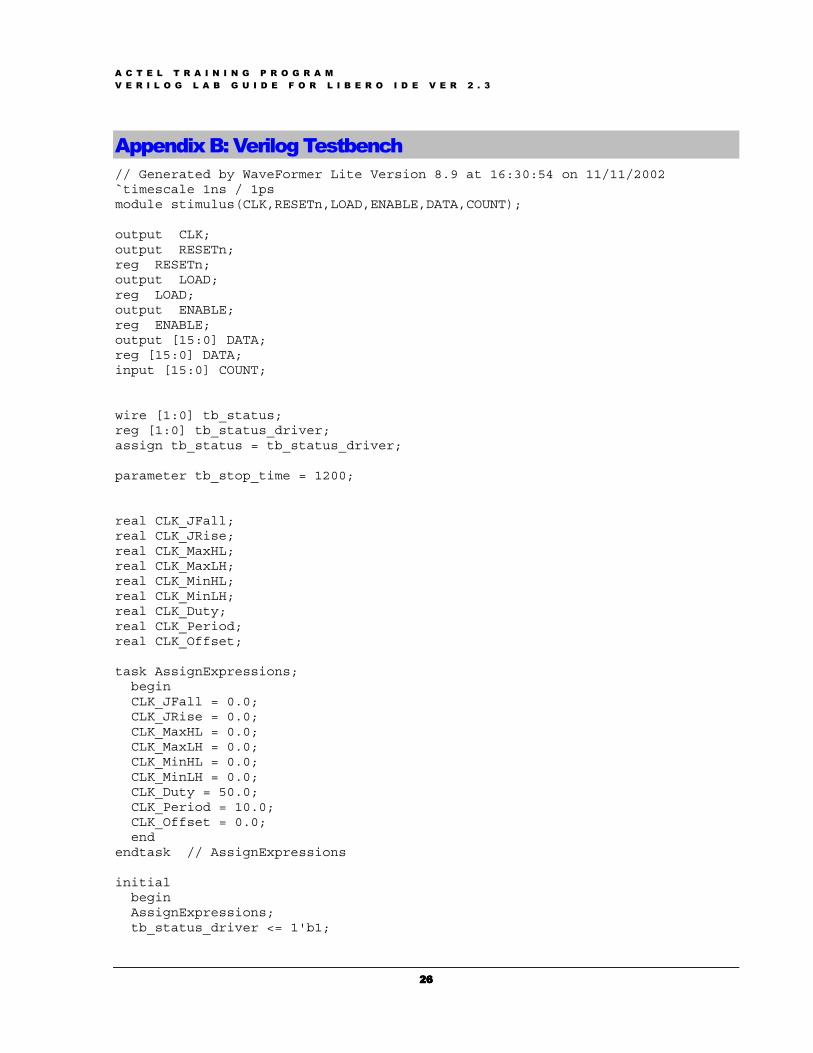
Appendix B: Verilog Testbench// Generated by WaveFormer Lite Version 8.9 at 16:30:54 on 11/11/2002`timescale 1ns / 1psmodule stimulus(CLK,RESETn,LOAD,ENABLE,DATA,COUNT);
output CLK;output RESETn;reg RESETn;output LOAD;reg LOAD;output ENABLE;reg ENABLE;output [15:0] DATA;reg [15:0] DATA;input [15:0] COUNT;
wire [1:0] tb_status;reg [1:0] tb_status_driver;assign tb_status = tb_status_driver;
parameter tb_stop_time = 1200;
real CLK_JFall;real CLK_JRise;real CLK_MaxHL;real CLK_MaxLH;real CLK_MinHL;real CLK_MinLH;real CLK_Duty;real CLK_Period;real CLK_Offset;
task AssignExpressions;beginCLK_JFall = 0.0;CLK_JRise = 0.0;CLK_MaxHL = 0.0;CLK_MaxLH = 0.0;CLK_MinHL = 0.0;CLK_MinLH = 0.0;CLK_Duty = 50.0;CLK_Period = 10.0;CLK_Offset = 0.0;end
endtask // AssignExpressions
initialbeginAssignExpressions;tb_status_driver <= 1'b1;
A C T E L T R A I N I N G P R O G R A MV E R I L O G L A B G U I D E F O R L I B E R O I D E V E R 2 . 3
27272727
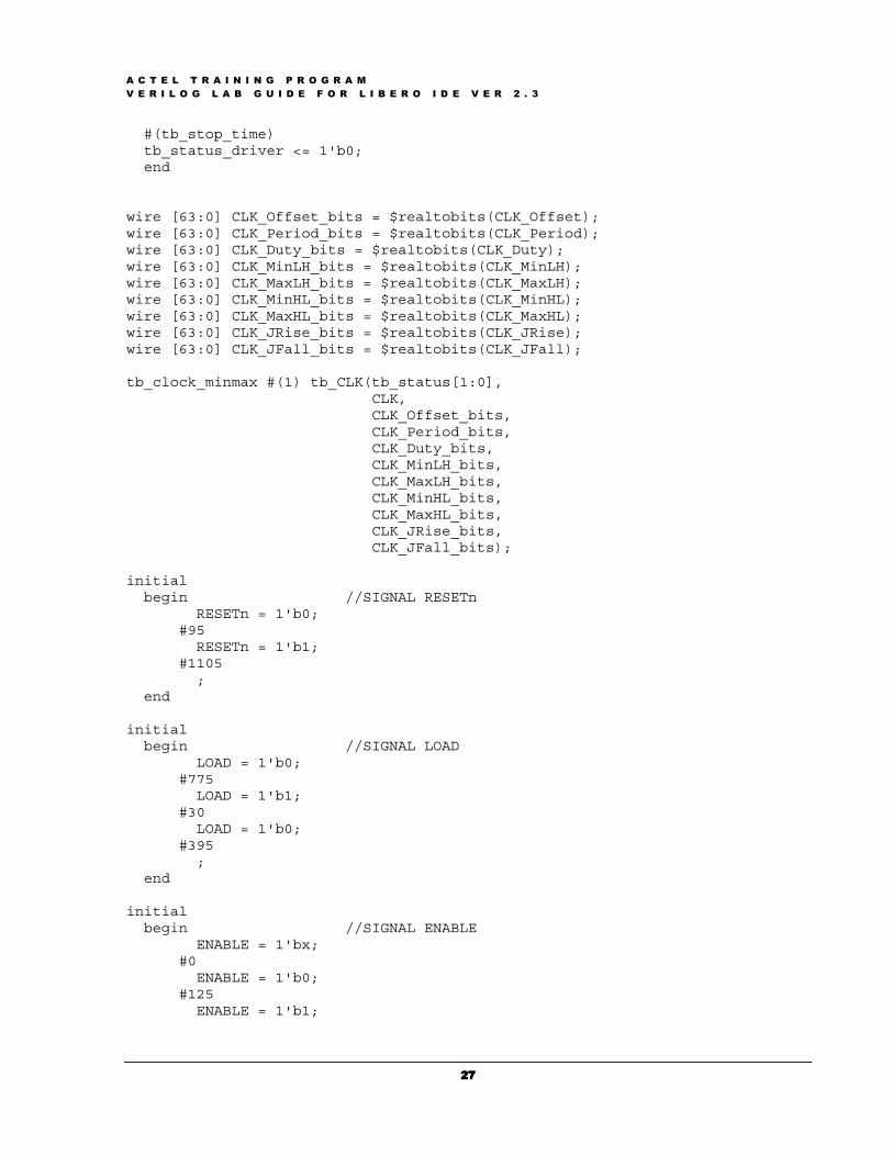
#(tb_stop_time)tb_status_driver <= 1'b0;end
wire [63:0] CLK_Offset_bits = $realtobits(CLK_Offset);wire [63:0] CLK_Period_bits = $realtobits(CLK_Period);wire [63:0] CLK_Duty_bits = $realtobits(CLK_Duty);wire [63:0] CLK_MinLH_bits = $realtobits(CLK_MinLH);wire [63:0] CLK_MaxLH_bits = $realtobits(CLK_MaxLH);wire [63:0] CLK_MinHL_bits = $realtobits(CLK_MinHL);wire [63:0] CLK_MaxHL_bits = $realtobits(CLK_MaxHL);wire [63:0] CLK_JRise_bits = $realtobits(CLK_JRise);wire [63:0] CLK_JFall_bits = $realtobits(CLK_JFall);
tb_clock_minmax #(1) tb_CLK(tb_status[1:0],CLK,CLK_Offset_bits,CLK_Period_bits,CLK_Duty_bits,CLK_MinLH_bits,CLK_MaxLH_bits,CLK_MinHL_bits,CLK_MaxHL_bits,CLK_JRise_bits,CLK_JFall_bits);
initialbegin //SIGNAL RESETn
RESETn = 1'b0;#95
RESETn = 1'b1;#1105
;end
initialbegin //SIGNAL LOAD
LOAD = 1'b0;#775
LOAD = 1'b1;#30
LOAD = 1'b0;#395
;end
initialbegin //SIGNAL ENABLE
ENABLE = 1'bx;#0
ENABLE = 1'b0;#125
ENABLE = 1'b1;
A C T E L T R A I N I N G P R O G R A MV E R I L O G L A B G U I D E F O R L I B E R O I D E V E R 2 . 3
28282828
#1075;
end
initialbegin //SIGNAL DATA
DATA = 16'h0000;#765
DATA = 16'hFFF8;#435
;end
initial#tb_stop_time $finish;
endmodule
module tb_clock_minmax(tb_status, CLK, offset_bits, period_bits, duty_bits,minLH_bits, maxLH_bits, minHL_bits, maxHL_bits, jRise_bits, jFall_bits);
parameter initialize = 0;
input [1:0] tb_status;output CLK;input [63:0] offset_bits;input [63:0] period_bits;input [63:0] duty_bits;input [63:0] minLH_bits;input [63:0] maxLH_bits;input [63:0] minHL_bits;input [63:0] maxHL_bits;input [63:0] jRise_bits;input [63:0] jFall_bits;
reg CLK;real offset;real period;real duty;real minLH;real maxLH;real minHL;real maxHL;real jRise;real jFall;real CLK_high;real CLK_low;
task DriveLHInvalidRegion;beginif ( (jRise + maxLH - minLH) > 0.0 )
beginCLK <= 1'bx;#((jRise + maxLH - minLH));end
A C T E L T R A I N I N G P R O G R A MV E R I L O G L A B G U I D E F O R L I B E R O I D E V E R 2 . 3
29292929
endendtask
task DriveHLInvalidRegion;beginif ( (jFall + maxHL - minHL) > 0.0 )
beginCLK <= 1'bx;#((jFall + maxHL - minHL));end
endendtask
alwaysbegin@(posedge tb_status[0])offset = $bitstoreal( offset_bits );period = $bitstoreal( period_bits );duty = $bitstoreal( duty_bits );minLH = $bitstoreal( minLH_bits );maxLH = $bitstoreal( maxLH_bits );minHL = $bitstoreal( minHL_bits );maxHL = $bitstoreal( maxHL_bits );jRise = $bitstoreal( jRise_bits );jFall = $bitstoreal( jFall_bits );if (period <= 0.0)
$display("Error: Period for clock %m is invalid (period=%f). Clockwill not be driven", period);
else if (duty <= 0.0)$display("Error: Duty for clock %m is invalid (duty=%f). Clock will
not be driven", duty);else
beginCLK_low = period * duty / 100;CLK_high = period - CLK_low;
if ( (offset + (minLH - jRise/2)) >= 0.0 )beginif (initialize)
CLK <= 1'b0; // drive initial state#(offset + (minLH - jRise/2));end
elsebegin // wait for xif (initialize)
CLK <= 1'bx; // in middle of X region, init to X#((jRise/2 + maxLH) + (offset))CLK <= 1'b1;#((CLK_high - (maxLH + jRise/2) + (minHL - jFall/2)))DriveHLInvalidRegion;CLK <= 1'b0;#((CLK_low - (maxHL + jFall/2) + (minLH - jRise/2)));
A C T E L T R A I N I N G P R O G R A MV E R I L O G L A B G U I D E F O R L I B E R O I D E V E R 2 . 3
30303030
endwhile ( tb_status[0] == 1'b1 )
begin : clock_loopDriveLHInvalidRegion;CLK <= 1'b1;#((CLK_high - (maxLH + jRise/2) + (minHL - jFall/2)))DriveHLInvalidRegion;CLK <= 1'b0;#((CLK_low - (maxHL + jFall/2) + (minLH - jRise/2)));end
endend
endmodule
//Test bench modulemodule testbench;
wire CLK;wire RESETn;wire LOAD;wire ENABLE;wire [15:0] DATA;wire [15:0] COUNT;
//Instantiation of the stimulus module.stimulus stimulus_0(CLK,RESETn,LOAD,ENABLE,DATA,COUNT);
//Instantiation of the product module.counter16 counter16_0(
.CLK(CLK),
.RESETn(RESETn),
.LOAD(LOAD),
.ENABLE(ENABLE),
.DATA(DATA),
.COUNT(COUNT));
endmodule