Embed Size (px)
Citation preview

REV. A–2–
AD7776/AD7777/AD7778–SPECIFICATIONSCLKIN = 8 MHz; RTN = O V; CREFIN = 10 nF; all specifications TMIN to TMAX unless otherwise noted.)
Parameter A Versions1 Units Conditions/Comments
DC ACCURACYResolution2 10 BitsRelative Accuracy ± 1 LSB max See TerminologyDifferential Nonlinearity ± 1 LSB max No Missing Codes; See TerminologyBias Offset Error ± 12 LSB max See TerminologyBias Offset Error Match 10 LSB max Between Channels, AD7777/AD7778 Only; See TerminologyPlus or Minus Full-Scale Error ± 12 LSB max See TerminologyPlus or Minus Full-Scale Error Match 10 LSB max Between Channels, AD7777/AD7778 Only; See Terminology
ANALOG INPUTSInput Voltage Range
All Inputs VBIAS ± VSWING V min/V maxInput Current +200 µA max VIN = VBIAS ± VSWING; Any Channel
REFERENCE INPUTREFIN 1.9/2.1 V min/V max For Specified PerformanceREFIN Input Current +200 µA max
REFERENCE OUTPUTREFOUT 1.9/2.1 V min/V max Nominal REFOUT = 2.0 VDC Output Impedance 5 Ω typReference Load Change ± 2 mV max For Reference Load Current Change of 0 to ±500 µA
± 5 mV max For Reference Load Current Change of 0 to ± 1 mAReference Load Should Not Change During Conversion
Short Circuit Current3 20 mA max See Terminology
LOGIC OUTPUTSDB0–DB9, BUSY/INT
VOL, Output Low Voltage 0.4 V max ISINK = 1.6 mAVOH, Output High Voltage 4.0 V min ISOURCE = 200 µAFloating State Leakage Current ± 10 µA maxFloating State Capacitance3 10 pF maxADC Output Coding Twos Complement
LOGIC INPUTSDB0–DB9, CS, WR, RD, CLKIN
Input Low Voltage, VINL 0.8 V maxInput High Voltage, VINH 2.4 V minInput Leakage Current 10 µA maxInput Capacitance3 10 pF max
CONVERSION TIMINGAcquisition Time 4.5 tCLKIN ns min See Terminology
5.5 tCLKIN + 70 ns maxSingle Conversion 14 tCLKIN ns maxDouble Conversion 28 tCLKIN ns maxtCLKIN 125/500 ns min/ns max Period of Input Clock CLKINtCLKIN High 50 ns min Minimum High Time for CLKINtCLKIN Low 40 ns min Minimum Low Time for CLKIN
POWER REQUIREMENTSVCC Range 4.75/5.25 V min/V max For Specified PerformanceICC, Normal Mode 15 mA max CS = RD = +5 V, CR8 = 0ICC, Power-Down Mode 1.5 mA max CR8 = 1. All Linear Circuitry OFFPower-Up Time to Operational
Specifications 500 µs max From Power-Down Mode
DYNAMIC PERFORMANCE See TerminologySignal to Noise and Distortion
S/(N+D) Ratio –56 dB min VIN = 99.88 kHz Full-Scale Sine Wave with fSAMPLING = 380.95 kHzTotal Harmonic Distortion (THD) –60 dB min VIN = 99.88 kHz Full-Scale Sine Wave with fSAMPLING = 380.95 kHzIntermodulation Distortion (IMD) –75 dB typ fa = 103.2 kHz, fb = 96.5 kHz with fSAMPLING = 380.95 kHz. Both
Signals Are Sine Waves at Half-Scale AmplitudeChannel-to-Channel Isolation –90 dB typ VIN = 100 kHz Full-Scale Sine Wave with fSAMPLING = 380.95 kHz
NOTES1Temperature range as follows: A = –40°C to +85°C.21 LSB = (2 × VSWING)/1024 = 1.95 mV for VSWING = 1.0 V.3Guaranteed by design, not production tested.
Specifications subject to change without notice.
(VCC = +5 V 5%; AGND = DGND = O V;

AD7776/AD7777/AD7778
–3–REV. A
TIMING SPECIFICATIONS1, 2(VCC = +5 V 5%; AGND = DGND = 0 V; all specifications TMIN to TMAX, unless otherwise noted.)
t3
t11
t10
t9 t8
FIRST CONVERSION
FINISHED(CR6 = 0)
SECOND CONVERSIONFINISHED (CR6 = 1)AD7777/AD7778 ONLY
t9
BUSY(CR8 = 0)
INT(CR8 = 1)
t10
WR, RD
Figure 3. BUSY/INT Timing
IOL
1.6mA
+2.1V
IOH
200µA
COUT
100pF
DB n
Figure 4. Load Circuit for Bus Timing Characteristics
t1
CS
t2
t4 t5
RD
DB0–DB9
Figure 1. Read Cycle Timing
t1
CS
t2
t6
WR
DB0–DB9
t3
t7
Figure 2. Write Cycle Timing
Parameter Label Limit at TMIN to TMAX Unit Test Conditions/Comments
INTERFACE TIMINGCS Falling Edge to WR or RD Falling Edge t1 0 ns minWR or RD Rising Edge to CS Rising Edge t2 0 ns minWR Pulsewidth t3 53 ns minCS or RD Active to Valid Data3, 4 t4 60 ns max Timed from Whichever Occurs LastBus Relinquish Time after RD3, 5 t5 10 ns min
45 ns maxData Valid to WR Rising Edge t6 55 ns minData Valid after WR Rising Edge t7 10 ns minWR Rising Edge to BUSY Falling Edge t8 1.5 tCLKIN ns min CR9 = 0
2.5 tCLKIN + 70 ns maxWR Rising Edge to BUSY Rising Edge orINT Falling Edge t9 19.5 tCLKIN + 70 ns max Single Conversion, CR6 = 0
t10 33.5 tCLKIN + 70 ns max Double Conversion, CR6 = 1WR or RD Falling Edge to INT Rising Edge t11 60 ns max CR9 = 1
NOTES1See Figures 1 to 3.2All input signals are specified with tr = tf = 5 ns (10% to 90% of 5 V) and timed from a voltage level of 1.6 V.3100% production tested. All other times are guaranteed by design, not production tested.4t4 is measured with the load circuit of Figure 4 and defined as the time required for an output to cross 0.8 V or 2.4 V.5t5 is derived from the measured time taken by the data outputs to change 0.5 V when loaded with the circuit of Figure 4. The measured time is then extrapolated backto remove the effects of charging or discharging the 100 pF capacitor. This means that the time t 5 quoted above is the true bus relinquish time of the device and, assuch, is independent of the external bus loading capacitance.
Specifications subject to change without notice.
AD7776/AD7777/AD7778
–4– REV. A
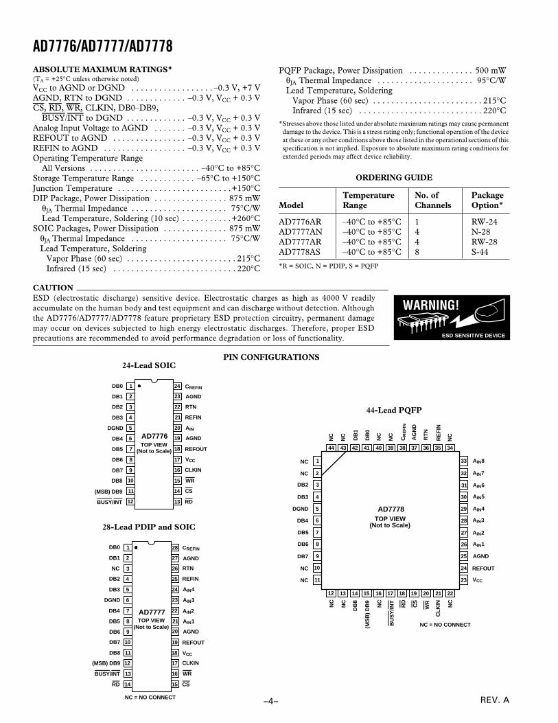
ABSOLUTE MAXIMUM RATINGS*(TA = +25°C unless otherwise noted)VCC to AGND or DGND . . . . . . . . . . . . . . . . . . –0.3 V, +7 VAGND, RTN to DGND . . . . . . . . . . . . . –0.3 V, VCC + 0.3 VCS, RD, WR, CLKIN, DB0–DB9,
BUSY/INT to DGND . . . . . . . . . . . . . –0.3 V, VCC + 0.3 VAnalog Input Voltage to AGND . . . . . . . –0.3 V, VCC + 0.3 VREFOUT to AGND . . . . . . . . . . . . . . . . –0.3 V, VCC + 0.3 VREFIN to AGND . . . . . . . . . . . . . . . . . . –0.3 V, VCC + 0.3 VOperating Temperature Range
All Versions . . . . . . . . . . . . . . . . . . . . . . . . –40°C to +85°CStorage Temperature Range . . . . . . . . . . . . –65°C to +150°CJunction Temperature . . . . . . . . . . . . . . . . . . . . . . . . .+150°CDIP Package, Power Dissipation . . . . . . . . . . . . . . . . 875 mW
θJA Thermal Impedance . . . . . . . . . . . . . . . . . . . . . 75°C/WLead Temperature, Soldering (10 sec) . . . . . . . . . . .+260°C
SOIC Packages, Power Dissipation . . . . . . . . . . . . . . 875 mWθJA Thermal Impedance . . . . . . . . . . . . . . . . . . . . . 75°C/WLead Temperature, Soldering
Vapor Phase (60 sec) . . . . . . . . . . . . . . . . . . . . . . . . 215°CInfrared (15 sec) . . . . . . . . . . . . . . . . . . . . . . . . . . . 220°C
ORDERING GUIDE
Temperature No. of PackageModel Range Channels Option*
AD7776AR –40°C to +85°C 1 RW-24AD7777AN –40°C to +85°C 4 N-28AD7777AR –40°C to +85°C 4 RW-28AD7778AS –40°C to +85°C 8 S-44
*R = SOIC, N = PDIP, S = PQFP
PQFP Package, Power Dissipation . . . . . . . . . . . . . . 500 mWθJA Thermal Impedance . . . . . . . . . . . . . . . . . . . . . 95°C/WLead Temperature, Soldering
Vapor Phase (60 sec) . . . . . . . . . . . . . . . . . . . . . . . . 215°CInfrared (15 sec) . . . . . . . . . . . . . . . . . . . . . . . . . . . 220°C
*Stresses above those listed under absolute maximum ratings may cause permanentdamage to the device. This is a stress rating only; functional operation of the deviceat these or any other conditions above those listed in the operational sections of thisspecification is not implied. Exposure to absolute maximum rating conditions forextended periods may affect device reliability.
PIN CONFIGURATIONS
44-Lead PQFP
7
8
9
10
11
6
5
4
3
2
1 33
32
31
30
29
28
27
26
25
24
23
18 19 20 21 22171615141312
39 38 37 36 35 3444 43 42 41 40
TOP VIEW(Not to Scale)
AD7778
NC
NC
NC
NC
NC
NC
NC
NC
NC
NC
NC
NC
NC
DB2
DB3
DGND
DB4
DB5
DB6
DB7
DB
1
DB
0
CR
EF
IN
RT
N
AG
ND
RE
FIN
AIN8
AIN7
AIN6
AIN5
AIN4
AIN3
AIN2
AIN1
AGND
REFOUT
VCC
DB
8
(MS
B)
DB
9
CL
KIN
BU
SY
/INT
RD
WRCS
NC = NO CONNECT
24-Lead SOIC
1
2
24
23
22
10 15
11
12
14
13
21
20
18
17
16
19
9
3
4
5
TOP VIEW(Not to Scale)7
8
6 AD7776
DB2
DB3
DGND
DB4
DB5
DB6
DB7
DB1
DB0 CREFIN
AGND
RTN
REFIN
AIN
AGND
REFOUT
VCC
DB8
(MSB) DB9
CLKIN
BUSY/INT RD
WR
CS
28-Lead PDIP and SOIC
1
2
24
23
22
10
15
11
12
14
13
21
20
17
16
9
3
4
5
7
8
6
18
19
TOP VIEW(Not to Scale)
28
27
26
25
AD7777
NC
NC = NO CONNECT
DB2
DB3
DGND
DB4
DB5
DB6
DB7
DB1
DB0
DB8
(MSB) DB9
BUSY/INT
CREFIN
AGND
RTN
REFIN
AGND
REFOUT
VCC
CLKIN
RD
WR
CS
AIN4
AIN3
AIN2
AIN1
WARNING!
ESD SENSITIVE DEVICE
CAUTIONESD (electrostatic discharge) sensitive device. Electrostatic charges as high as 4000 V readilyaccumulate on the human body and test equipment and can discharge without detection. Althoughthe AD7776/AD7777/AD7778 feature proprietary ESD protection circuitry, permanent damagemay occur on devices subjected to high energy electrostatic discharges. Therefore, proper ESDprecautions are recommended to avoid performance degradation or loss of functionality.

AD7776/AD7777/AD7778
–5–REV. A
PIN FUNCTION DESCRIPTION
Mnemonic Description
VCC +5 V Power Supply.
AGND Analog Ground.
DGND Digital Ground. Ground reference for digital circuitry.
DB0–DB9 Input/Output Data Bus. This is a bidirectional data port from which ADC output data may be read and to whichcontrol register data may be written.
BUSY/INT Busy/Interrupt Output. Active low logic output indicating A/D converter status. This logic output has two modesof operation depending on whether location CR9 of the control register has been set low or high:If CR9 is set low, the BUSY/INT output behaves as a BUSY signal. The BUSY signal goes low and stays low for theduration of a single conversion, or if simultaneous sampling has been selected, BUSY stays low for the duration ofboth conversions.If CR9 is set high, BUSY/INT output behaves as an INTERRUPT signal. The INT signal goes low and remains lowafter either a single conversion is completed or after a double conversion is completed if simultaneous sampling hasbeen selected. With CR9 high, the falling edge of WR or RD resets the INT line high.
CS Chip Select Input. The device is selected when this input is low.
WR Write Input (Active Low). It is used in conjunction with CS to write data to the control register. Data is latched to theregisters on the rising edge of WR. Following the rising edge of WR, the analog input is acquired and a conversion isstarted.
RD Read Input (Active Low). It is used in conjunction with CS to enable the data outputs from the ADC registers.
AIN1–8 Analog Inputs 1–8. The analog input range is VBIAS ± VSWING where VBIAS and VSWING are defined by the referencevoltage applied to REFIN. Input resistance between any of the analog input pins and AGND is 10 kΩ or greater.
REFIN Voltage Reference Input. The AD7776/AD7777/AD7778 are specified over a voltage reference range of 1.9 V to 2.1 Vwith a nominal value of 2.0 V. This REFIN voltage provides the VBIAS and VSWING levels for the input channel(s).VBIAS is equal to REFIN and VSWING is nominally equal to REFIN/2. Input resistance between this REFIN pin andAGND is 10 kΩ or greater.
REFOUT Voltage Reference Output. This pin provides the internal voltage reference, which is nominally 2.0 V. It can providethe bias voltage (VBIAS) for the input channel(s).
CREFIN Reference Decoupling Capacitor. A 10 nF capacitor must be connected from this pin to AGND to ensure correctoperation of the high speed ADC.
RTN Signal Return Path for the input channel(s). Normally RTN is connected to AGND at the package.
CIRCUIT DESCRIPTIONADC Transfer FunctionFor all versions, an input signal of the form VBIAS ± VSWING isexpected. This VBIAS signal level operates as a pseudo ground towhich all input signals must be referred. The VBIAS level isdetermined by the voltage applied to the REFIN pin. This canbe driven by an external voltage source or, alternatively, by theonboard 2 V reference, available at REFOUT. The magnitudeof the input signal swing is equal to VBIAS/2 (or REFIN/2) and isset internally. With a REFIN of 2 V, the analog input signal levelvaries from 1 V to 3 V, i.e., 2 ± 1 V. Figure 5 shows the transferfunction of the ADC and its relationship to VBIAS and VSWING.The half-scale two's complement code of the ADC, 000 Hex (000000 0000 Binary), occurs at an input voltage equal to VBIAS. Theinput full-scale range of the ADC is equal to 2 VSWING, so that thePlus Full-Scale transition (1FE to 1FF) occurs at a voltage equal toVBIAS + VSWING – 1.5 LSBs, and the minus full-scale code transi-tion (200 to 201) occurs at a voltage VBIAS – VSWING + 0.5 LSBs.
ADCOUTPUT
CODE(HEX)
1FF1FE
202201200
000
VBIAS–VSWING
VBIAS
VBIAS+VSWINGANALOG INPUT, VIN
Figure 5. ADC Transfer Function

AD7776/AD7777/AD7778
–6– REV. A
AD7778CR5 CR4 CR3 Function0 0 0 Select AIN10 0 1 Select AIN20 1 0 Select AIN30 1 1 Select AIN41 0 0 Select AIN51 0 1 Select AIN61 1 0 Select AIN71 1 1 Select AIN8
CR6: Determines whether operation is on a single channel orsimultaneous sampling on two channels. Location CR6 is a“don’t care” for the AD7776.
CR6 Function0 Single channel operation. Channel select
address is contained in locations CR0–CR2.1 Two channels simultaneously sampled
and sequentially converted. Channelselect addresses contained in locationsCR0–CR2 and CR3–CR5.
CR7: Determines whether the device is in the normal operatingmode or in the half-scale test mode.
CR7 Function0 Normal Operating Mode1 Half-Scale Test Mode
In the half-scale test mode, REFIN is internally connected as ananalog input(s). In this mode, locations CR0–CR2 and CR3–CR5are all “don’t cares” since it is REFIN which is converted. Forthe AD7777 and AD7778, the contents of location CR6 stilldetermine whether a single or a double conversion is carried outon the REFIN level.
CR8: Determines whether the device is in the normal operatingmode or in the power-down mode.
CR8 Function0 Normal Operating Mode1 Power-Down Mode
In the power-down mode all linear circuitry is turned off and theREFOUT output is weakly (5 kΩ) pulled to AGND. The inputimpedance of the analog inputs and of the REFIN input remainsthe same in either normal mode or power-down mode. Seeunder Circuit Description—Power-Down Mode.
CR9: Determines whether BUSY/INT output flag goes low andremains low during conversion(s) or else goes low and remainslow after the conversion(s) is (are) complete.
CR9 BUSY/INT Functionality0 Output goes low and remains low during
conversion(s).1 Output goes low and remains low after conversion(s)
is (are) complete.
CONTROL REGISTERThe control register is 10-bit wide and can only be written to.On power-on, all locations in the control register are automati-cally loaded with 0s. For the single channel AD7776, locationsCR0 to CR6 of the control register are “don’t cares.” For thequad channel AD7777, locations CR2 and CR5 are “don’tcares.” Individual bit functions are described below.
CR0–CR2: Channel Address Locations. Determines which channelis selected and converted for single-channel operation. For simulta-neous sampling operation, CR0–CR2 holds the address of one ofthe two channels to be sampled.
AD7776CR2 CR1 CR0 FunctionX* X X Select AIN1*X = Don’t Care
AD7777CR2 CR1 CR0 FunctionX* 0 0 Select AIN1X 0 1 Select AIN2X 1 0 Select AIN3X 1 1 Select AIN4*X = Don’t Care
AD7778CR2 CR1 CR0 Function0 0 0 Select AIN10 0 1 Select AIN20 1 0 Select AIN30 1 1 Select AIN41 0 0 Select AIN51 0 1 Select AIN61 1 0 Select AIN71 1 1 Select AIN8
CR3–CR5: Channel Address Locations. Only applicable for simul-taneous sampling with the AD7777 or AD7778 when CR3–CR5holds the address of the second channel to be sampled.
AD7777
CR5 CR4 CR3 FunctionX* 0 0 Select AIN1X 0 1 Select AIN2X 1 0 Select AIN3X 1 1 Select AIN4*X = Don’t Care

AD7776/AD7777/AD7778
–7–REV. A
ADC Conversion Start TimingFigure 6 shows the operating waveforms for the start of a conver-sion cycle. On the rising edge of WR, the conversion cycle startswith the acquisition and tracking of the selected ADC channel,AIN1–8. The analog input voltage is held 40 ns (typically) afterthe first rising edge of CLKIN following four complete CLKINcycles. If tD in Figure 6 is greater than 12 ns, the falling edge ofCLKIN as shown is seen as the first falling clock edge. If tD isless than 12 ns, the first falling clock edge to be recognized doesnot occur until one cycle later.
Following the “hold” on the analog input(s), two completeCLKIN cycles are allowed for settling purposes before the MSBdecision is made. The actual decision point occurs approximately40 ns after the rising edge of CLKIN as shown in Figure 6. Twomore CLKIN cycles are allowed for the second MSB decision.The succeeding bit decisions are made approximately 40 nsafter each rising edge of CLKIN until the conversion is complete.At the end of conversion, if a single conversion has beenrequested (CR6 = 0), the BUSY/INT line changes state (asprogrammed by CR9) and the SAR contents are transferred tothe first register ADCREG1. The SAR is then reset in readiness fora new conversion. If simultaneous sampling has been requested(CR6 = 1), no change occurs in the status of the BUSY/INToutput, and the ADC automatically starts the second conversion.At the end of this conversion, the BUSY/INT line changes state(as programmed by CR9) and the SAR contents are transferredto the second register, ADCREG2.
tD*
CLKIN
VIN
WR
CHANNEL ACQUISITION
40nsTYP
40nsTYP
'HOLD' DB9 (MSB)
* TIMING SHOWN FOR tD GREATER THAN 12ns
Figure 6. ADC Conversion Start Timing
Track-and-HoldThe track-and-hold (T/H) amplifiers on the analog input(s) ofthe AD7776/AD7777/AD7778 allow the ADC to accuratelyconvert an input sine wave of 2 V peak-peak amplitude up to afrequency of 189 kHz, the Nyquist frequency of the ADC whenoperated at its maximum throughput rate of 378 kHz. Thismaximum rate of conversion includes conversion time and thetime between conversions. Because the input bandwidth of thetrack-and-hold is much greater than 189 kHz, the input signalshould be band limited to avoid folding unwanted signals intothe band of interest.
Power-DownThe AD7776/AD7777/AD7778 can be placed in a power-downmode simply by writing a logic high to location CR8 of thecontrol register. The following changes are effected immediatelyupon writing a “1” to location CR8:
• Any conversion in progress is terminated.
• If a conversion is in progress, the leading edge of WR immedi-ately drives the BUSY/INT output high.
• All the linear circuitry is turned off.
• The REFOUT output stops being driven and is weakly (5 kΩ)pulled to analog ground.
Control inputs CS, WR, and RD retain their purpose while theAD7776/AD7777/AD7778 is in power-down mode. If noconversions are in progress when the AD7776/AD7777/AD7778is placed into power-down mode, the contents of the ADCregisters, ADCREG1 and ADCREG2, are retained duringpower-down and can be read as normal. On returning to normaloperating mode, a new conversion (or conversions, dependenton CR6) is automatically started. Upon completion, the invalidconversion results are loaded into the ADC registers, losing theprevious valid results.
To achieve the lowest possible power consumption in thepower-down mode, special attention must be paid to the state ofthe digital and analog inputs and outputs:
• Because each analog input channel sees a resistive divider toAGND, the input resistance of which does not changebetween normal and power-down modes, driving the analoginput signals to 0 V or as close as possible to 0 V minimizesthe power dissipated in the input signal conditioning circuitry.
• Similarly, the REFIN input sees a resistive divider to AGND,the input resistance of which does not change betweennormal and power-down modes. If an external reference isbeing used, then driving this reference input to 0 V or asclose as possible to 0 V minimizes the power dissipated inthe input signal conditioning circuitry.
• Since the REFOUT pin is pulled to AGND via, typically, a5 kΩ resistor, any voltage above 0 V that this output may bepulled to by external circuitry dissipates unnecessary power.
• Digital inputs CS, WR, and RD should all be held at VCC oras close as possible. CLKIN should be held as close aspossible to either 0 V or VCC.
• Since the BUSY/INT output is actively driven to a logic high,any loading on this pin to 0 V dissipates power.
The AD7776/AD7777/AD7778 comes out of the power-downmode when a Logic “0” is written to location CR8 of thecontrol register. Note that the contents of the other locationsin the control register are retained when the device is placed inpower-down and are valid when power is restored. However,coming out of power-down provides an opportunity to reloadthe complete contents of the control register without anyextra instructions.

AD7776/AD7777/AD7778
–8– REV. A
Microprocessor Interfacing CircuitsThe AD7776/AD7777/AD7778 family of ADCs is intended tointerface to DSP machines such as the ADSP-2101, ADSP-2105,the TMS320 family and microcontrollers such as the 80C196family.
Figure 7 shows the AD7776/AD7777/AD7778 interfaced to theTMS320C10 at 20.5 MHz and the TMS320C14 at 25 MHz.Figure 8 shows the interface with the TMS320C25 at 40 MHz.Note that one wait state is required with this interface. TheADSP-2101-50 and the ADSP-2105-40 interface is shown inFigure 9. One wait state is required with these machines.
*ADDITIONAL PINS OMITTED FOR CLARITY
ADDRESS BUS
DATA BUSD15–D0
TMS320C10-20.5TMS320C14-25
A11–A0
WE
(C10) DEN(C14) REN
CS
DB9–DB0
RD
WR
AD7776/AD7777/AD7778*
ADDRDECODE
Figure 7. AD7776/AD7777/AD7778 to TMS320C10 andTMS320C14 Interface
ADDRESS BUS
DATA BUS
*ADDITIONAL PINS OMITTED FOR CLARITY
CS
DB9–DB0
RD
WR
D15–D0
A15–A0
IS
READY
MSC
STRBR/W
TMS320C25-40
ADDRDECODE AD7776/
AD7777/AD7778*
Figure 8. AD7776/AD7777/AD7778 to TMS320C25 Interface
Figure 10 shows the interface with the 80C196KB at 12 MHzand the 80C196KC at 16 MHz. One wait state is required withthe 16 MHz machine. The 80C196 is configured to operatewith a 16-bit multiplexed address/data bus.
Table I provides a truth table for the AD7776/AD7777/AD7778and summarizes their microprocessor interfacing features. Notethat a read instruction to any of the devices while a conversionis in progress immediately stops that conversion and returnsunreliable data over the data bus.
*ADDITIONAL PINS OMITTED FOR CLARITY
ADDRESS BUS
DATA BUS
CS
DB9–DB0
RD
WR
D23–D6
A13–A0
WR
RD
ADSP-2101-50ADSP-2105-40
ADDRDECODE
ENDMS AD7776/AD7777/AD7778*
Figure 9. AD7776/AD7777/AD7778 to ADSP-2101 andADSP-2105 Interface
*ADDITIONAL PINS OMITTED FOR CLARITY
DATA BUS (10)
CS
DB9–DB0
AD7776/AD7777/AD7778*
RD
WR
ADDRESS BUS
WR
RD
80C196KB-1280C196KC-16
AD15–AD6(PORT 4)
ALE‘373
LATCH
ADDRDECODER
AD7–AD0(PORT 3)
Figure 10. AD7776/AD7777/AD7778 to 80C196 Interface

AD7776/AD7777/AD7778
–9–REV. A
Table I. AD7776/AD7777/AD7778 Truth Table for Microprocessor Interfacing
CS RD WR DB0–DB9 Function/Comments
1 X* X* High Z Data Port High Impedance
0 1 j CR Data Load control register (CR) data to control register and start a conversion.
0 k 1 ADC Data ADC data placed on data bus. Depending upon location CR6 of the control register, one or twoRead instructions are required.
If CR6 is low, i.e., single-channel conversion selected, a read instruction returns the contents ofADCREG1. Succeeding read instructions continue to return the contents of ADCREG1.
If CR6 is high, i.e., simultaneous sampling (double conversion) selected, the first read instructionreturns the contents of ADCREG1 while the second read instruction returns the contents ofADCREG2. A third read instruction returns ADCREG1 again, the fourth ADCREG2, etc.
*X = Don’t Care
DESIGN INFORMATIONLayout HintsEnsure that the layout for the printed circuit board has the digi-tal and analog grounds separated as much as possible. Take carenot to run any digital track alongside an analog signal track.Guard (screen) the analog input(s) with RTN.
Establish a single-point analog ground separate from the logicsystem ground and as close as possible to the AD7776/AD7777/AD7778. Both the RTN and AGND pins on the AD7776/AD7777/AD7778 and all other signal grounds should be con-nected to this single point analog ground. In turn, this starground should be connected to the digital ground at one pointonly—preferably at the low impedance power supply itself.
Low impedance analog and digital power supply common returnsare important for correct operation of the devices, so make thefoil width for these tracks as wide as possible.
To ensure a low impedance +5 V power supply at the actual VCC
pin, it is necessary to use bypass capacitors from the pin itself toDGND. A 4.7 µF tantalum capacitor in parallel with a 0.1 µFceramic capacitor is sufficient.
ADC CorruptionExecuting a read instruction to the AD7776/AD7777/AD7778while a conversion is in progress immediately halts the conversionand returns invalid data over the data bus. The BUSY/ INToutput pin should be monitored closely and all read instructionsto the AD7776/AD7777/AD7778 prevented while this outputshows that a conversion is in progress.
Executing a write instruction to the AD7776/AD7777/AD7778while a conversion is in progress immediately halts the conversion,while the falling edge of WR driving the BUSY/INT output high.The analog input(s) is sampled as normal, and a new conversionsequence (dependent upon CR6) is started.
ADC Conversion TimeAlthough each conversion takes only 14 CLKIN cycles, it can takebetween 4.5 and 5.5 CLKIN cycles to acquire the analog input(s)after the WR input goes high and before any conversions start.
TERMINOLOGYRelative AccuracyFor the AD7776/AD7777/AD7778, relative accuracy or endpointnonlinearity is the maximum deviation, in LSBs, of the ADC’sactual code transition points from a straight line drawn betweenthe endpoints of the ADC transfer function.
Differential NonlinearityDifferential nonlinearity is the difference between the measuredchange and the ideal 1 LSB change between any two adjacentcodes. A specified maximum differential nonlinearity of ±1 LSBensures no missed codes.
Bias Offset ErrorFor an ideal 10-bit ADC, the output code for an input voltageequal to VBIAS should be midscale. The bias offset error is thedifference between the actual midpoint voltage for midscale codeand VBIAS, expressed in LSBs.
Bias Offset Error MatchThis is a measure of how closely the bias offset errors of allchannels track each other. The bias offset error match of anychannel must be no further away than 10 LSBs from the biasoffset error of any other channel, regardless of whether thechannels are independently sampled or simultaneously sampled.
Plus and Minus Full-Scale ErrorThe input channels of the ADC can be considered to havebipolar (positive and negative) input ranges, but are referred toVBIAS (or REFIN) instead of AGND. Positive full-scale error forthe ADC is the difference between the actual input voltagerequired to produce the plus full-scale code transition and the idealinput voltage (VBIAS + VSWING –1.5 LSB), expressed in LSBs.Minus full-scale error is similarly specified for the minus full-scalecode transition, relative to the ideal input voltage for thistransition (VBIAS – VSWING + 0.5 LSB). Note that the full-scaleerrors for the ADC input channels are measured after theirrespective bias offset errors have been adjusted out.
Plus and Minus Full-Scale Error MatchThis is a measure of how closely the full-scale errors of allchannels track each other. The full-scale error match of any channelmust be no further away than 10 LSBs from the respectivefull-scale error of any other channel, regardless of whether thechannels are independently sampled or simultaneously sampled.

AD7776/AD7777/AD7778
–10– REV. A
Short Circuit CurrentThis is defined as the maximum current which flows eitherinto or out of the REFOUT pin if this pin is shorted to anypotential between 0 V and VCC. This condition can be allowedfor up to 10 seconds provided that the power dissipation of thepackage is not exceeded.
Signal-to-Noise and Distortion Ratio, S/(N+D)Signal-to-noise and distortion ratio, S/(N+D), is the ratio of therms value of the measured input signal to the rms sum of allother spectral components below the Nyquist frequency, includ-ing harmonics, but excluding dc. The value for S/(N+D) isgiven in decibels.
Total Harmonic Distortion, THDTotal harmonic distortion is the ratio of the rms sum of the firstfive harmonic components to the rms value of a full-scale inputsignal and is expressed in decibels. For the AD7776/AD7777/AD7778, total harmonic distortion (THD) is defined as:
20
22
32
42
52
62 1 2
1log
V V V V V
V
+ + + +( )
where V1 is the rms amplitude of the fundamental and V2,V3, V4, V5, and V6 are the rms amplitudes of the individualharmonics.
Intermodulation Distortion, IMDWith inputs consisting of sine waves at two frequencies, fa and fb,any active device with nonlinearities creates distortion products,of order (m + n), at sum and difference frequencies of mfa + nfb,where m, n = 0, 1, 2, 3. Intermodulation terms are those for whichm or n is not equal to zero. For example, the second order termsinclude (fa + fb) and (fa – fb) and the third order terms include(2 fa + fb), (2 fa – fb), (fa + 2 fb), and (fa – 2 fb).
Channel-to-Channel IsolationChannel-to-channel isolation is a measure of the level of cross-talkbetween channels. It is measured by applying a full-scale 100 kHzsine wave signal to any one of the input channels and monitoringthe remaining channels. The figure given is the worst case acrossall channels.
DIGITAL SIGNAL PROCESSING APPLICATIONSIn digital signal processing (DSP) application areas like voicerecognition, echo cancellation, and adaptive filtering, the dynamiccharacteristics S/(N+D), THD, and IMD of the ADC are critical.The AD7776/AD7777/AD7778 are specified dynamically as wellas with standard dc specifications. Because the track/holdamplifier has a wide bandwidth, an antialiasing filter should beplaced on the analog inputs to avoid aliasing high frequency noiseback into the bands of interest.
The dynamic performance of the ADC is evaluated by applying asine wave signal of very low distortion to a single analog inputwhich is sampled at 380.95 kHz. A fast Fourier transform (FFT)plot or histogram plot is then generated from which the signal tonoise and distortion, harmonic distortion, and dynamic differentialnonlinearity data can be obtained. Similarly, for intermodulationdistortion, an input signal consisting of two pure sine waves atdifferent frequencies is applied to the AD7776/AD7777/AD7778.
Figure 11 shows a 2048-point FFT plot for a single channel ofthe AD7778 with an input signal of 99.88 kHz. The SNR is58.71 dB. It can be seen that most of the harmonics are buriedin the noise floor. It should be noted that the harmonics aretaken into account when calculating the S/(N+D).
0
–90
–80
0
–60
–40
–20
99.88
SIG
NA
L A
MP
LIT
UD
E –
dB
FREQUENCY – kHz
INPUT FREQUENCY =99.88kHzSAMPLE FREQUENCY =380.95kHzSNR = 58.7dBTA = 25C
Figure 11. ADC FFT Plot
The relationship between S/(N+D) and resolution (n) is ex-pressed by the following equation:
S N D n dB+( ) = +( )6 02 1 76. .
This is for an ideal part with no differential or integral linearityerrors. These errors cause a degradation in S/(N+D). By work-ing backwards from the above equation, it is possible to get ameasure of ADC performance expressed in effective numberof bits (n).
n effective
S N D dB( ) =+( ) ( ) − 1 76
6 02
.
.
The effective number of bits plotted versus frequency for asingle channel of the AD7778 is shown in Figure 12. The effec-tive number of bits is typically 9.5.
10.0
7.5189.2
9.0
8.0
8.5
0
9.5
INPUT FREQUENCY – kHz
EF
FE
CT
IVE
NU
MB
ER
OF
BIT
S
SAMPLE FREQUENCY = 378.4kHzTA = 24C
Figure 12. Effective Number of Bits vs. Frequency

AD7776/AD7777/AD7778
–11–REV. A
RTN is tied to REFOUT, then the analog input range becomes0 V to 2 V. The fixed 2 V analog input voltage span of the ADCcan range from 1 V to 3 V (RTN = 0 V) to 0 V to 2 V (RTN =2 V), i.e., with proper biasing, an input signal range from 0.3 Vto 2.3 V can be covered. Both the relative accuracy and differen-tial nonlinearity performance remain essentially unchanged inthis mode, while the SNR and THD performance are typically2 dB to 3 dB worse than standard.
Changing the Analog Input Voltage RangeBy biasing the RTN pin above AGND, it is possible to changethe analog input voltage range from its VBIAS ± VSWING format toa more traditional 0 V to VREF range. The new input range canbe described as
V to V REFINOFFSET OFFSET +( )where 0 V ≤ VOFFSET ≤ 1 V. To produce this range, the RTN pinmust be biased to (REFIN – 2 VOFFSET). For instance, if
OUTLINE DIMENSIONS
24-Lead Standard Small Outline Package [SOIC]Wide Body
(RW-24)Dimensions shown in millimeters and (inches)
CONTROLLING DIMENSIONS ARE IN MILLIMETERS; INCH DIMENSIONS(IN PARENTHESES) ARE ROUNDED-OFF MILLIMETER EQUIVALENTS FORREFERENCE ONLY AND ARE NOT APPROPRIATE FOR USE IN DESIGN
COMPLIANT TO JEDEC STANDARDS MS-013AD
0.32 (0.0126)0.23 (0.0091)
80
0.75 (0.0295)0.25 (0.0098)
45
1.27 (0.0500)0.40 (0.0157)
SEATINGPLANE
0.30 (0.0118)0.10 (0.0039)
0.51 (0.020)0.33 (0.013)
2.65 (0.1043)2.35 (0.0925)
1.27 (0.0500)BSC
24 13
12110.65 (0.4193)10.00 (0.3937)
7.60 (0.2992)7.40 (0.2913)
15.60 (0.6142)15.20 (0.5984)
COPLANARITY0.10
28-Lead Standard Small Outline Package [SOIC]Wide Body
(RW-28)Dimensions shown in millimeters and (inches)
CONTROLLING DIMENSIONS ARE IN MILLIMETERS; INCH DIMENSIONS(IN PARENTHESES) ARE ROUNDED-OFF MILLIMETER EQUIVALENTS FORREFERENCE ONLY AND ARE NOT APPROPRIATE FOR USE IN DESIGN
COMPLIANT TO JEDEC STANDARDS MS-013AE
0.32 (0.0126)0.23 (0.0091)
80
0.75 (0.0295)0.25 (0.0098)
45
1.27 (0.0500)0.40 (0.0157)
SEATINGPLANE
0.30 (0.0118)0.10 (0.0039)
0.51 (0.0201)0.33 (0.0130)
2.65 (0.1043)2.35 (0.0925)
1.27 (0.0500)BSC
28 15
141
18.10 (0.7126)17.70 (0.6969)
10.65 (0.4193)10.00 (0.3937)
7.60 (0.2992)7.40 (0.2913)
COPLANARITY0.10

AD7776/AD7777/AD7778
–12– REV. A
OUTLINE DIMENSIONS
28-Lead Plastic Dual-in-Line Package [PDIP](N-28)
Dimensions shown in millimeters and (inches)
4.95 (0.1949)3.18 (0.1252 )
0.38 (0.0150)0.20 (0.0079)
15.87 (0.6248)15.24 (0.6000)
28
1 14
15
14.73 (0.5799)12.32 (0.4850)
39.70 (1.5630)35.10 (1.3819)
SEATINGPLANE
1.52 (0.0598)0.38 (0.0150)
6.35(0.2500)
MAX
0.56 (0.0220)0.36 (0.0142)
5.05 (0.1988)3.18 (0.1252)
3.81(0.1500)MIN
2.54(0.1000)
BSC
1.77(0.0697)
MAX
CONTROLLING DIMENSIONS ARE IN MILLIMETERS; INCH DIMENSIONS(IN PARENTHESES) ARE ROUNDED-OFF MILLIMETER EQUIVALENTS FORREFERENCE ONLY AND ARE NOT APPROPRIATE FOR USE IN DESIGN
44-Lead Plastic Quad Flatpack [PQFP](S-44)
Dimensions shown in millimeters
13.20 BSC SQ
0.80BSC
10.00 BSC SQ
0.450.29
2.202.001.80
2.45MAX
1.030.880.73
80.8SEATING
PLANE
TOP VIEW(PINS DOWN)
1
33
34
11
12
23
22
44
COPLANARITY0.10
COMPLIANT TO JEDEC STANDARDS MS-022-AB
PIN 1
0.25 MAX
Revision HistoryLocation Page
10/02—Data Sheet changed from REV. 0 to REV. A.
Changes to SPECIFICATIONS . . . . . . . . . . . . . . . . . . . . . . . . . . . . . . . . . . . . . . . . . . . . . . . . . . . . . . . . . . . . . . . . . . . . . . . . . . . . 2
Changes to ORDERING GUIDE . . . . . . . . . . . . . . . . . . . . . . . . . . . . . . . . . . . . . . . . . . . . . . . . . . . . . . . . . . . . . . . . . . . . . . . . . . . 4
Changes to Total Harmonic Distortion, THD section . . . . . . . . . . . . . . . . . . . . . . . . . . . . . . . . . . . . . . . . . . . . . . . . . . . . . . . . . . . 10
Changes to OUTLINE DIMENSIONS . . . . . . . . . . . . . . . . . . . . . . . . . . . . . . . . . . . . . . . . . . . . . . . . . . . . . . . . . . . . . . . . . . . . . 12
C01
196–
0–10
/02(
A)
PR
INT
ED
IN U
.S.A
.